1. Introduction
In information displays, human-computer interaction plays a crucial role for the evolution of intelligentization [
1]. From the conventional mouse and keyboard to the state of art of capacitive sensing touch and voice recognition input, human-computer interactions are becoming more and more efficient and convenient [
2]. Currently, in small and medium-sized screen multipoint direct touch technologies such as capacitive [
3], resistive [
4], surface acoustic [
5] and infrared light occluded [
6] are satisfactory and widely used. Which can realize well-known what you touch is what you get by users’ fingers.
However, as the enlargement of screen sizes for affording more audiences, particularly in education and conference, the interaction range has exceeded human body's physical limitation. In that case, existing infrared light occlusion and capacitive technologies relying on the direct contact of human fingers or pointers with the screens often confine users around the devices and even worse some positions are not directly touchable. Therefore, remote control interactions that can extend the ‘touch’ range of human body are keenly needed.
Based on the working principles, the techniques of remote touch can be categorized into inertial sensing, imaging recognition, and optical touch. The typical devices based on inertial gyro technology are fly mice and cyborg rumble Pads. In which, the acceleration of the device’s movements is measured by the embedded gyros and then it is converted to the moving of cursors on the screen. By using gyro, users can remotely control the display devices in free space like desk typed optical mice without physical limitation [
7,
8]. Inertial sensor-based interaction devices have the advantages in visual reality and wearable devices which can facilitate the sensing of the user’s movements in three-dimensional space [
9,
10]. However, since the locating of cursors comes from the relative acceleration data of devices’ movement other than from the absolute indication points of the control devices, it means that users must shake or swing the devices repeatedly until the cursor is moved to the desired positions on the screen, thus unconformable experience of the delay in reaction and inaccuracy in direction often occurs. It seems that, inertial gyro-based interaction devices are more suitable to virtual reality than to flat panel displays, where users do not need to see the hands of themselves in real word.
As for the imaging recognition technology based on cameras, the interaction between users and displays comes from the detection of the movements or gesture changes of the hands or fingers which are usually attached with markers for enhancing the imaging recognition ability of the computers [
11,
12,
13]. The drawback of computation vision-based interaction is that it requires the cameras to capture the movement of the directors in real time thus the operation zones are limited by the cameras field of view and focus depth which bring about the experience of confinement.
Optical touch technology employs lights as input signals where the position of the curser is directly obtained from the absolute shined spots of the laser beams, obeying the people’s habit of three points one line. In that case, the laser pointers act as an extension of the user's hand, where the positions illuminated by the laser pointers are instantly in consistence with the interaction points. Consequently, it works more closely to users’ intuition, reducing the users learning threshold and enabling more comfortable experience. For optical touch, there are two primary methods for achieving illumination positions according to the distribution of photodetectors. For the Planar Array Type (PAT) [
14,
15,
16], the optical sensing units are embedded into each pixel of the display panel. For the Line Array Type (LAT) [
17], the detectors are set around the four edges of transparent micro structured film. The micro structures on the film are used to trap the incident lights and convert them to four guiding modes propagating along the film in total internal reflection. Eventually, the four guiding beams reach to the line detector arrays, where they were converted to electric signals. Finally, the illumination positions of the lights on the screen are reconstructed by the cross points between the two virtual lines obtained from the corresponding coordinates of the detector arrays. The LAT has the advantage of lower cost than that of PAT. However, the LAT is suffering from the large scattering loss which hinder its application in large size display. To solve issue of LAT, a remote optical touch technology based on grating antenna light trapping by using laser beams as input signals has been proposed and single-point touch has been demonstrated[
18]. Although the above optical touch technology affords accurate and instant location of the cursors, however ghost points are inevitable if more than one beam is input. Thus, in existing remote optical touch systems, multi-point operation has not been realized yet.
Since analog light inputs will cause ghost points, to distinguish the beams from each other, we load digital signals with different parameters on each incident beams. Specifically, in our scheme, pulse-width modulation (PWM) is applied on the beams where each beam has a different pulse width. When these beams illuminate the phototransistors, they generate pulsed photocurrents corresponding to the modulation characteristics. The photocurrents are converted into voltages via reference resistors and are subsequently changed into digital signals by analog-to-digital converters. Consequently, as the digital voltage retains the pulse width of the original beam, differentiation of the digital voltages allows computers to distinguish incident beams from each other. Based upon the process, remote multi-point optical touch is realized. This innovation not only integrates the advantages of multi-touch into three-dimensional space human-computer interaction, but also creates a more natural and intuitive three-dimensional space interaction.
2. Materials and Methods
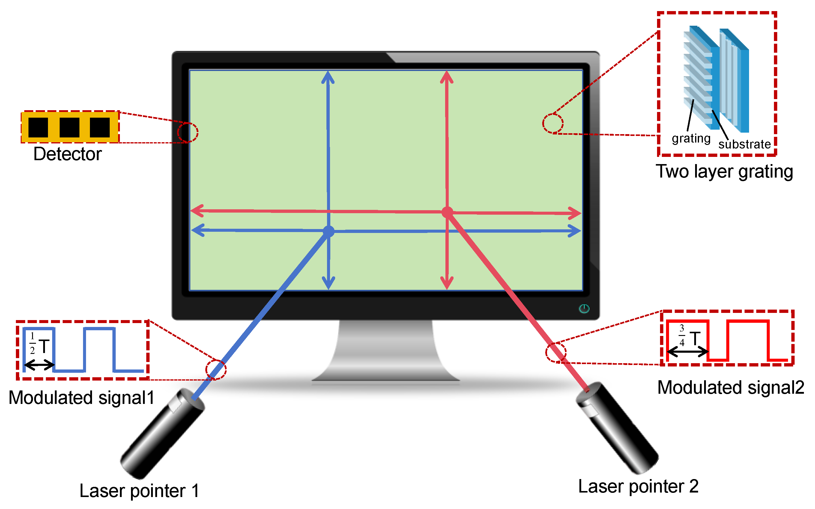
The architecture of the multi-point optical interaction system is shown in
Figure 1. The system consists of three main components: two amplitude-modulated laser pointers for optical signal input, two layers of transparent optical waveguide film with grating antennas on the front surface, and optoelectronic detector arrays attached surrounding the four edges of the waveguide films.
Different pulses are modulated on the infrared laser pointers to divide inputs from different users, enabling mutual-interference free multi-user interaction. The two layer of optical waveguide films, accompanied by optoelectronic detector arrays, is sandwiched between the backlight and the liquid crystal panel. One-dimensional grating antennas with gating vectors along X direction on the front surface of the first layer film and Y direction on the second lay film are set to couple the incident lights into the waveguide and direct them to the sensor arrays that discern touching positions.
2.1. The Design of Grating Antenna
The core component of this touch system is the subwavelength grating antennas which are designed to couple the laser beams with a wavelength of 980nm into the waveguide layers for obtaining position information. The antennas satisfy the grating coupling equation as shown in Equation 1. Where, n and n
i are the refractive indices of the substrate and the air respectively,
is the diffraction angle propagates in the optical waveguide films and
is the incidence angle in the air, m is an integer representing the order of diffraction, is the wavelength of the incident laser lights, and T is the period of the grating antennas.
As shown in
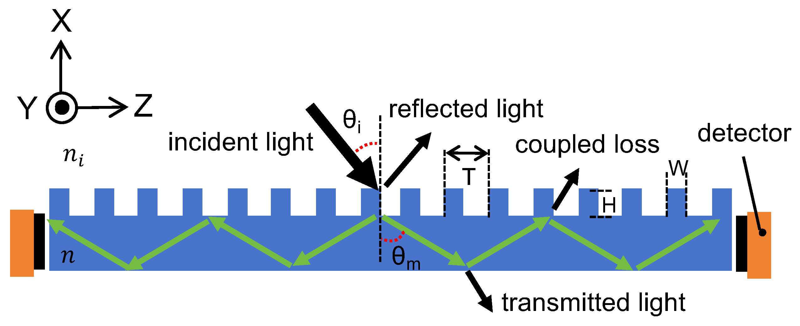
Figure 2, the incident laser light is coupled by the grating antenna to propagate along the optical waveguide films in total internal reflection (TIR). It is then detected by the photosensitive detectors located on the four edges of the film. It should be noted that the propagating light inside the waveguide will be partly lost out of the waveguide at the TIR spots by grating antennas, which should be considered in the later structure design.
As depicted in
Figure 2, the amount of the light that reach to the detectors around the edges of the optical films are decided by the coupling efficiency of the grating antenna. The appropriate parameters should be carefully chosen to obtain as much as of the coupling efficiency.
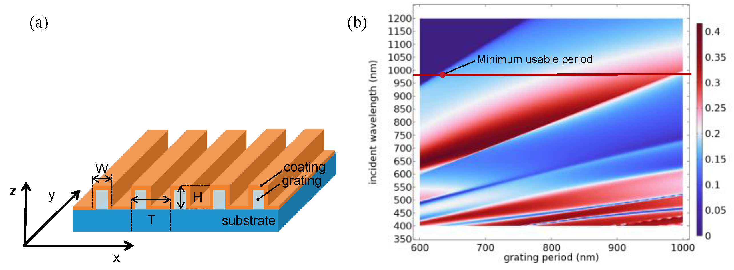
Figure 3a illustrates the device structure of the periodical grating antenna, where a unit structure consists of an air cover layer, a coating layer (TiO2), a grating layer, and an optical waveguide film as the substrate. The grating and the substrate are of the same material of polycarbonate (PC). The numerical simulation and optimization of the diffraction efficiency of the grating antenna were conducted by using finite element method based COMSOL software. In the simulation, the refractive indices of air, TiO2 coating, and PC grating are 1.0, 2.3, and 1.57, respectively. Based on the fabrication results, the grating height
is 250nm and the duty factor is 0.5. As mentioned above, there are periodical recoupled loss at the TIR spots in the optical waveguide, thus for reducing loss the number of the recoupled spots should be decreased. According to the Equation (1), the diffraction angle of +1 order is greater than that of the -1 order, meaning that +1 order diffracted propagating light has longer diffracted step inside the waveguide which can effectively reduce the recoupled losses. Consequently, only+1 order diffraction light is simulated and chosen to work as waveguiding light signals. The simulated +1 order diffraction efficiency of grating antennas with different periods for normal incident angle and wavelengths ranging from 350nm to 1200nm is illustrated in
Figure 3b. As indicated of the red dot line in the simulation, in the pitch range of 630-980m, the grating antenna can convert the incident beams with wavelength of 980nm into TIR waveguide lights in the +1-order diffraction. In this work, the period of 650nm is selected to prove the concept.
2.2. Hardware Architecture
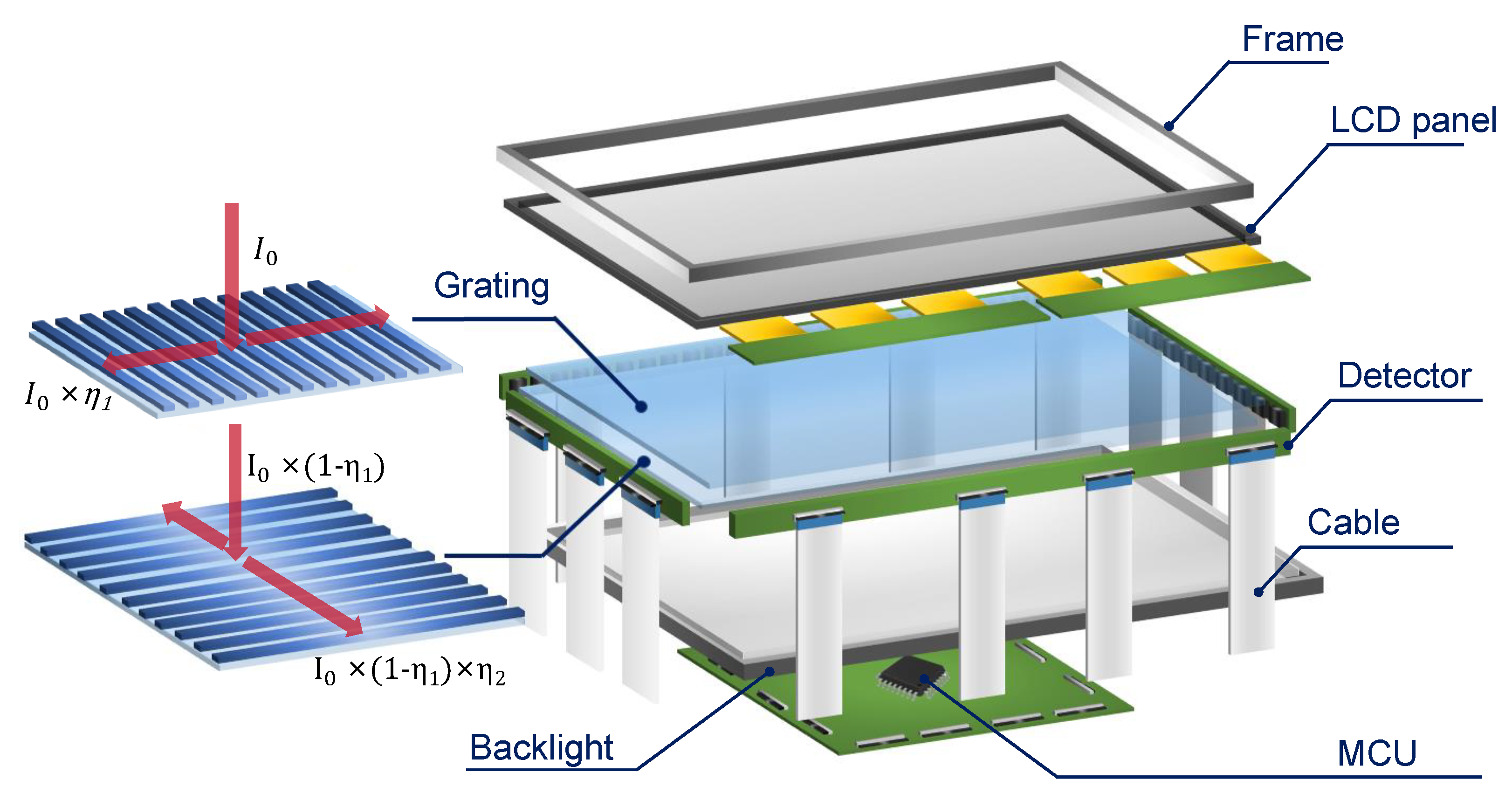
The primary components of the prototype optical touch system are depicted in
Figure 4. It consists of an 18-inch(365mm*235mm) liquid crystal display (LCD) panel, two layers of transparent PC optical wave guide films, a backlight module, a detection sensing circuit, and a micro controller unit (MCU). The grating antenna are fabricated by hot embossing Nano-imprinting process on the front surfaces of the optical films. Titanium dioxide was deposited on the grating layer as high refractive index coating to increase the diffraction efficiency for obtaining as high as of the optical signals reaching the photodetectors [
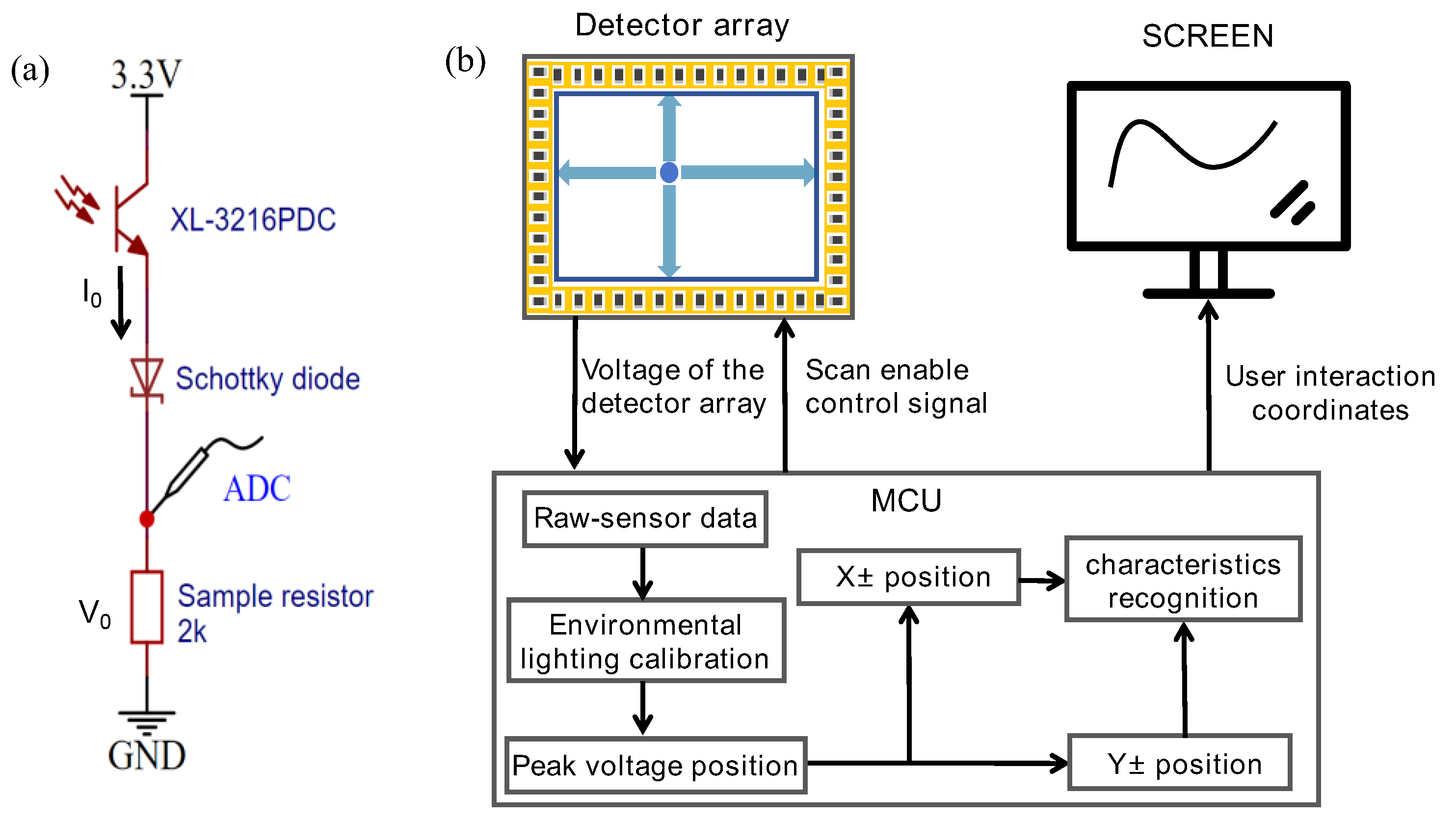
19]. As illustrated by the red lines on the grating antenna, the incident infrared lights pass through the LCD panel at first and then shines the grating antenna, where it is coupled inside the PC film by diffraction and subsequently propagate along the XY axis. The phototransistors (XL-3216PDC from Xinglight) with a sensing area of 2.0mm by 1.6mm, were organized into arrays, where each array comprises 14 detectors with a space of 2mm next to each other. To cover the entire display screen, seven arrays were respectively placed at the top and bottom edges, and four arrays were placed on each of the left and right edges.
As depicted in
Figure 5a, each detector unit consists of a phototransistor, a Schottky diode, and a sampling resistor. When waveguide light reaches the phototransistor, the photocurrent
varies with the intensity of the light, producing a waveform that reflects the modulation of the incident light pulses. The photocurrent I
0 then flows along the circuit, passing through the Schottky diode and the sampling resistor before grounding. Due to the negligible forward resistance of the Schottky diode, the photocurrent primarily generates a voltage
across the sampling resistor. The voltage
, which has the same period and duty cycle as the incident light, is converted into a digital voltage signal
by the ADC after the detector array receives an enable signal.
Figure 5b demonstrates the entire interaction process via the grating antenna-based recognition module, where the MCU sequentially activates the detector array, collects and processes digital voltage data to determine interaction points, and then those points are displayed on the screen. The MCU controls the sequential operation of 22 detector arrays by scanning enable signals. During operation, the ADC continuously samples voltages of the 14 sensors in each array four times. When all arrays have completed their operation, the MCU obtains a two-dimensional array of voltage samples
, where p denotes detector positions ranging from 0 to 307, and t denotes four consecutive sampling times range from 0 to 3.
The raw signals need to be calibrated since they contain noise of ambient light. During calibration, the detector voltage without laser illumination is subtracted from the raw data , resulting in a voltage only from the laser pointers. After that, the data are compared to determine the positions of the peak voltage, which is greater than the voltages of the adjacent sensors.
Subsequently, those peak voltage positions are grouped into two categories based on whether they align with the X-axis or Y-axis. The continuous sampling characteristics of each peak voltage location are identified. The interaction points are determined by drawing intersecting lines between positions on the X and Y axes that share the same characteristics. Finally, those interaction points are displayed on the screen, for indicating users’ interested locations and helping to complete the interactive process.
2.3. Modulation and Demodulation Methods
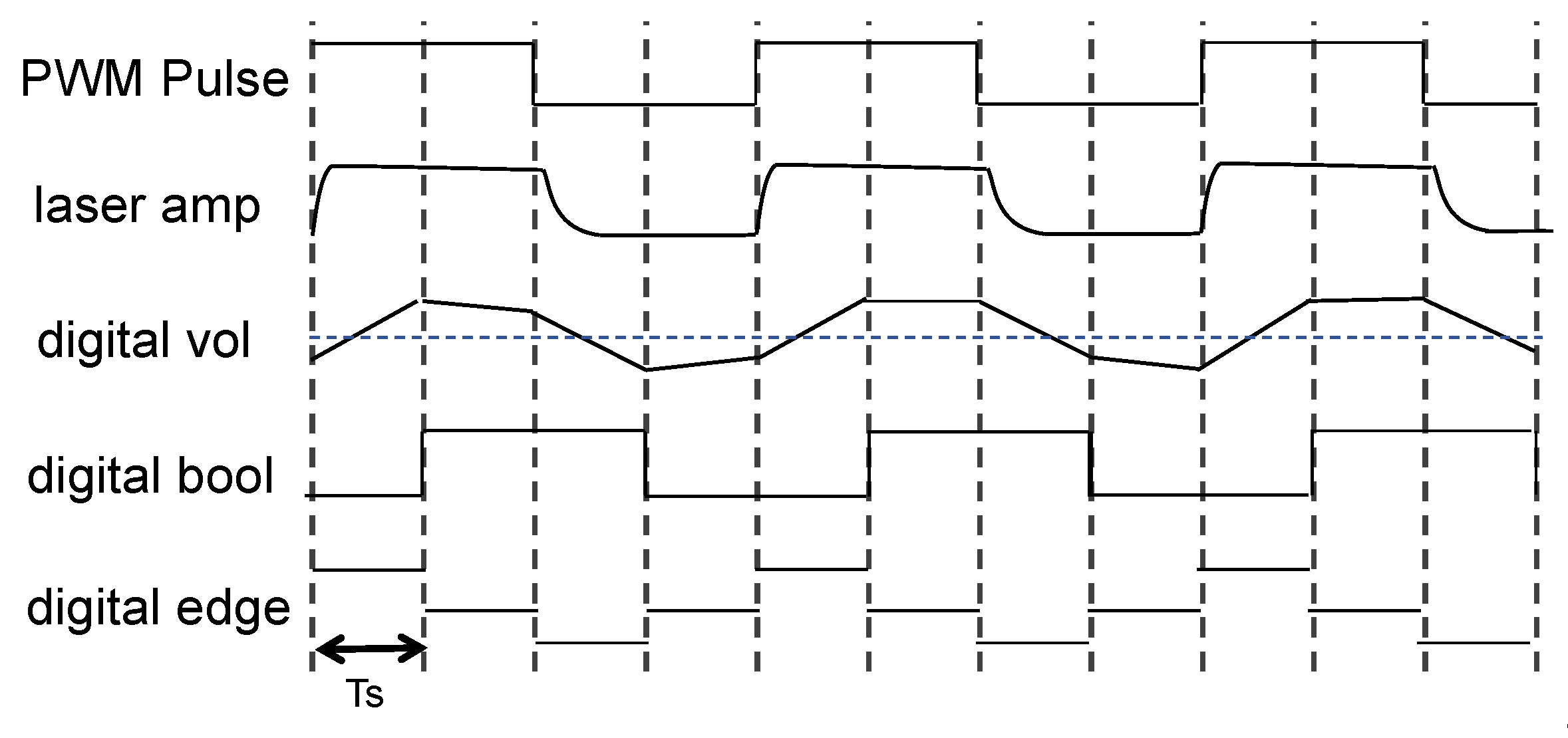
As illustrated in
Figure 6, the pulses endow the amplitudes of the laser beams with distinct periodic and pulse width characteristics. Then, the characteristics of the laser amplitude are converted into digital voltage signal by the detection circuit. By demodulating those digital voltage characteristics, remote and simultaneous multi-user optical touch is achieved.
To improve response rate while maintaining multi-user detection, we utilized duty cycle detection (DCD) to demodulate PWM. As shown in
Figure 6, by using dynamic thresholds, which is half of the maximum voltage from the last four scans, the digital voltages are converted into binary values. Those Boolean values are then categorized based on their transition trends: a change from 0 to 1 is identified as a rising edge (1), a transition from 1 to 0 is labeled as a falling edge (-1), while no change represents a flat state (0). The duration between rising and falling edges determines the demodulation result of pulse width, and the span between two consecutive rising edges constitutes the modulation period.
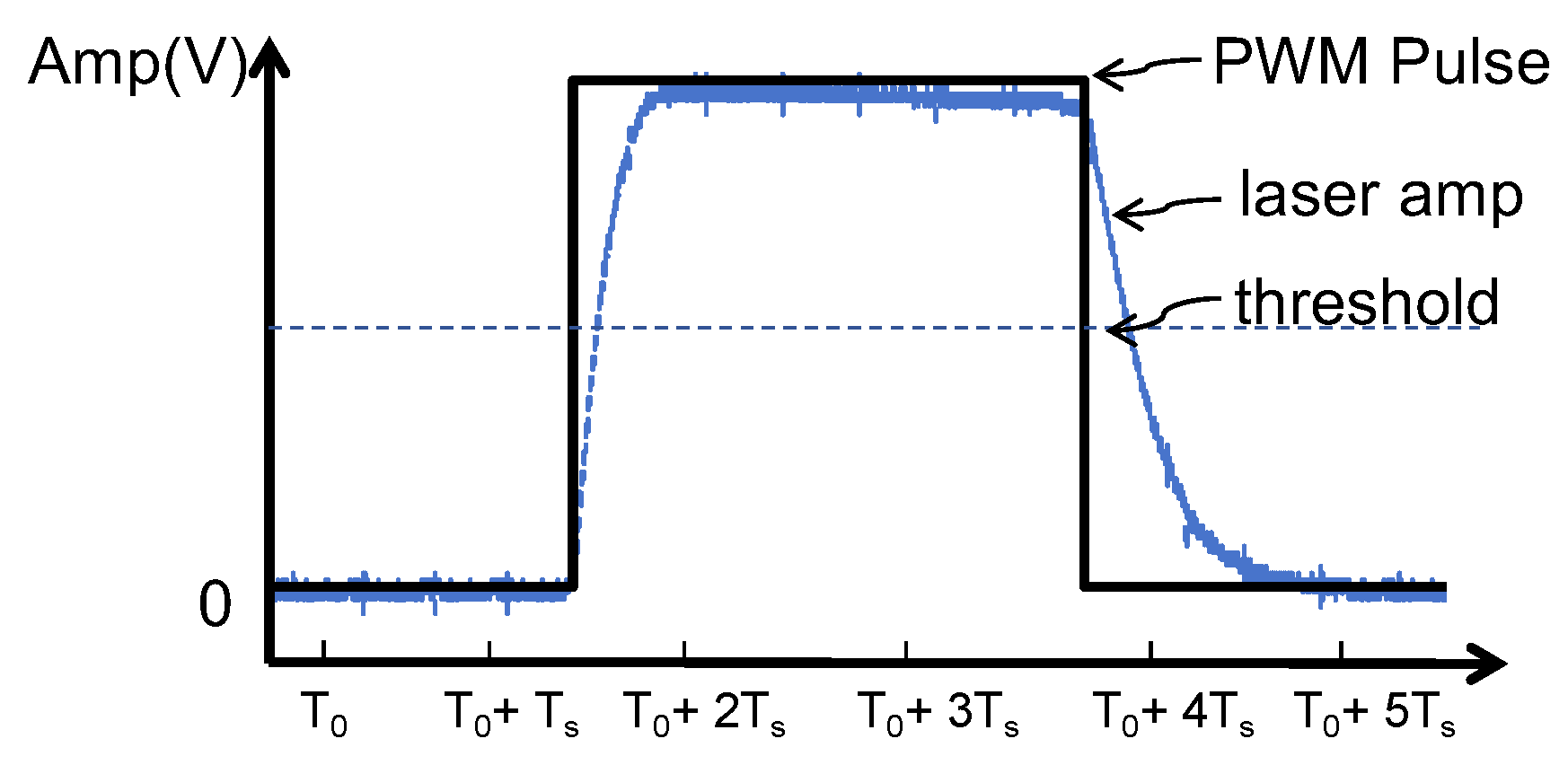
In the demodulation process, the precision of frequency and pulse width recovery depends on the digital voltage’s fidelity in replicating the characteristics of PWM signal. However, the generation of the photocurrent requires a transient time to reach its peak and revert to the baseline dark current state, which is both 20μs in this case. The overlong rise and fall times result in a compression and stretching of the pulse respectively, thus constrain the selection of modulation period and pulse width.
Figure 7 exemplifies how the laser amplitude is distorted from the original PWM waveform. The duration above the threshold constitutes the pulse width, hence the signal distortion can be deducted as Equation (2).
In equation (2), Tup and Tdown respectively represent the rise and fall times of the detector. W is the duty cycle of the modulation, while T denotes the modulation period. Mismatch between the fall times and the rise times generates pattern distortion, resulting in the incorrect identification of pulse width.
The establishment of dynamic thresholds is contingent upon the accurate capture of the peak voltage. As depicted in
Figure 7, the peak duration is influenced by the rise times, where the longer the rise times, the more pronounced distortion. If the peak duration of the signal is less than sampling interval
Ts of 25μs, some of the peak voltages might be leaked, leading to the failure of dynamic thresholds establishment. To ensure the acquisition of peak voltage, the modulation signal must fulfill the following conditions:
In equation (3), considering the sampling interval and rise edges, we selected a pulse width above 45μs to circumvent sampling distortion. Furthermore, to reduce the coding length and decrease scanning times, the pulse width is set to 50μs and 80μs with a modulation period of 100μs.
3. Experiment Process and Result Analysis
3.1. Experimental Setup
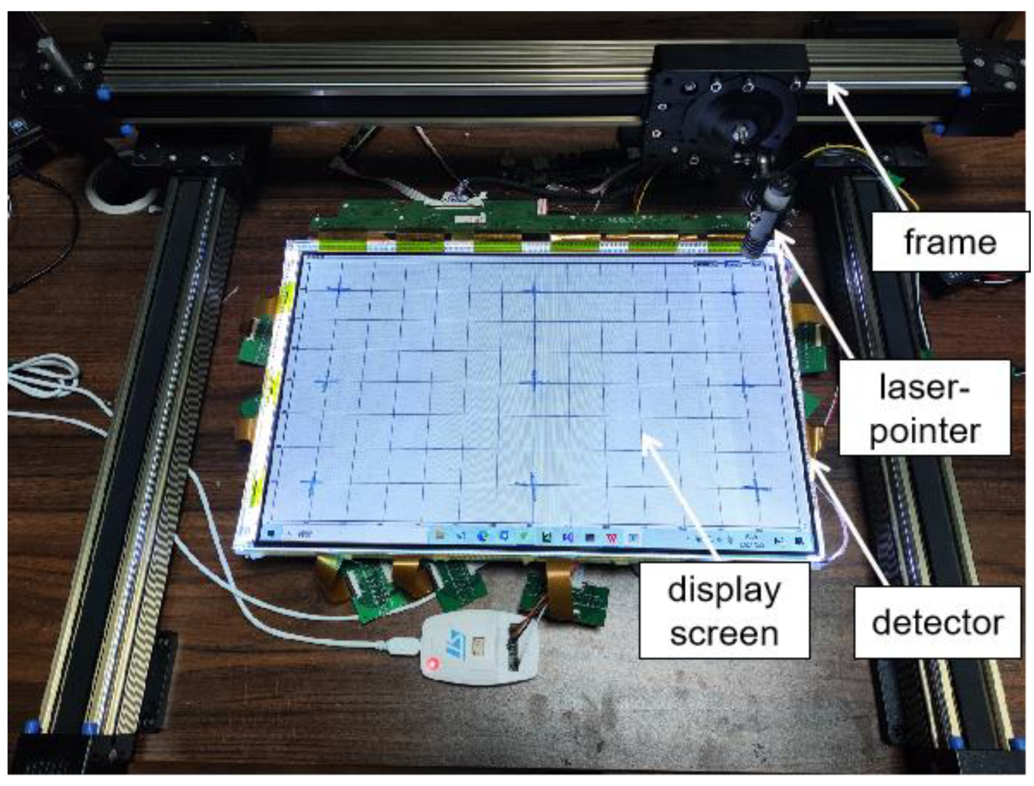
The measurement setup of the optical touch system is shown in
Figure 8, where the optical touch screen is placed in the center of the setup, surrounded by detector arrays. The arrays are directly connected to an MCU, and the interaction points identified by the MCU are displayed on the screen. Two infrared laser pointers with emitting wavelength of 980nm, operation voltage range of 2.0V to 2.3V and working current range of 600mA to 800mA were used in the experiment. The amplitude modulation of the laser pointers was achieved through a PWM generator (N76E003 microcontroller chip). The PWM generator can generate pulse signals with adjustable duty cycles from 0% to 100% and frequencies ranging from 1kHz to 100kHz. A laser pointer is fixed on the Y direction tracks, with its light beam perpendicular to the screen. During the experiment, the laser pointer can scan of the screen by moving the tracks in X and Y directions.
3.2. Static Accuracy Experiment
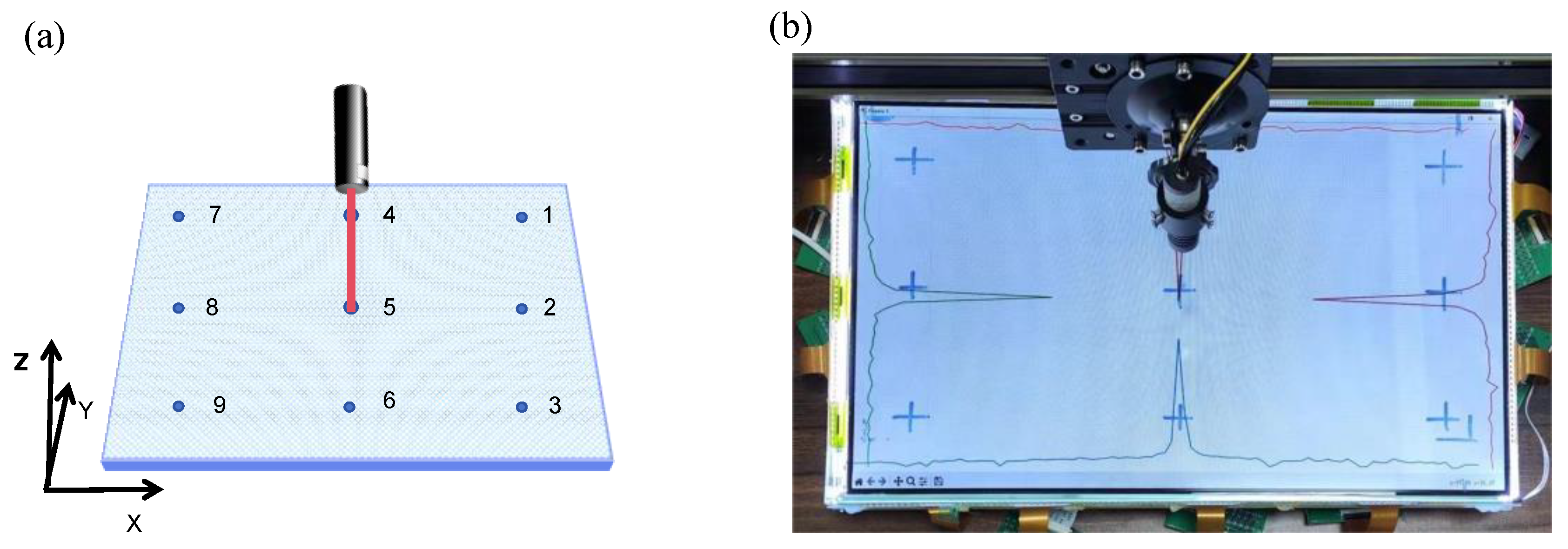
As illustrated in
Figure 9a, to evaluate the detection errors of the different positions on the screen, nine equidistantly spaced points measurement was applied. The target points were evenly distributed on the screen with a spacing of 8cm along the Y axis and 15cm along the X axis. At each incident point, the calculated positions of the cursors are simultaneously recorded for error measurements. The error is defined as the distance between the intersection point and the actual incident point along the X and Y axes. For proof of concept, in this work, the incident light beams are perpendicular to the display plane.
One of the typical voltage sampling results of the sensor arrays is plotted in
Figure 9b, corresponding to incident position of No.5. As expected, distinct peaks at the X- and Y-axis can be clearly observed. This demonstrates how the intersection point of two lines drawn on the X-axis and Y-axis at the voltage peak positions can be used as an interaction point.
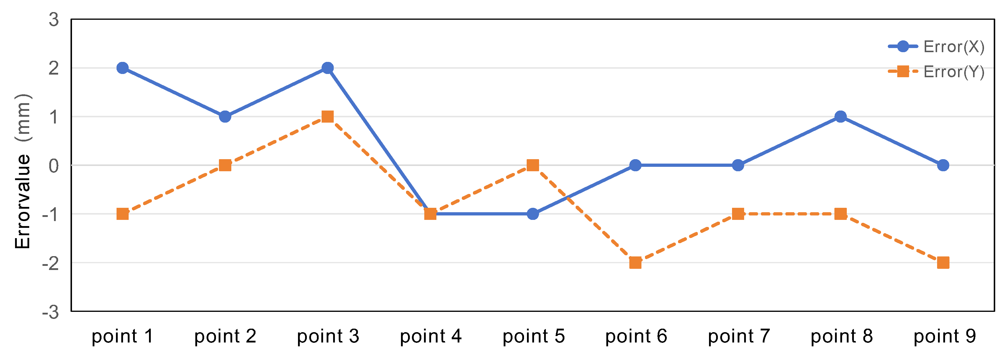
The errors obtained from nine experiments are shown in
Figure 9c. The maximum errors are of 2mm on both the X-axis and the Y-axis, with both average errors of 1mm. These errors are mainly caused by the 3mm distance between the detectors even after quadratic curve fitting method.
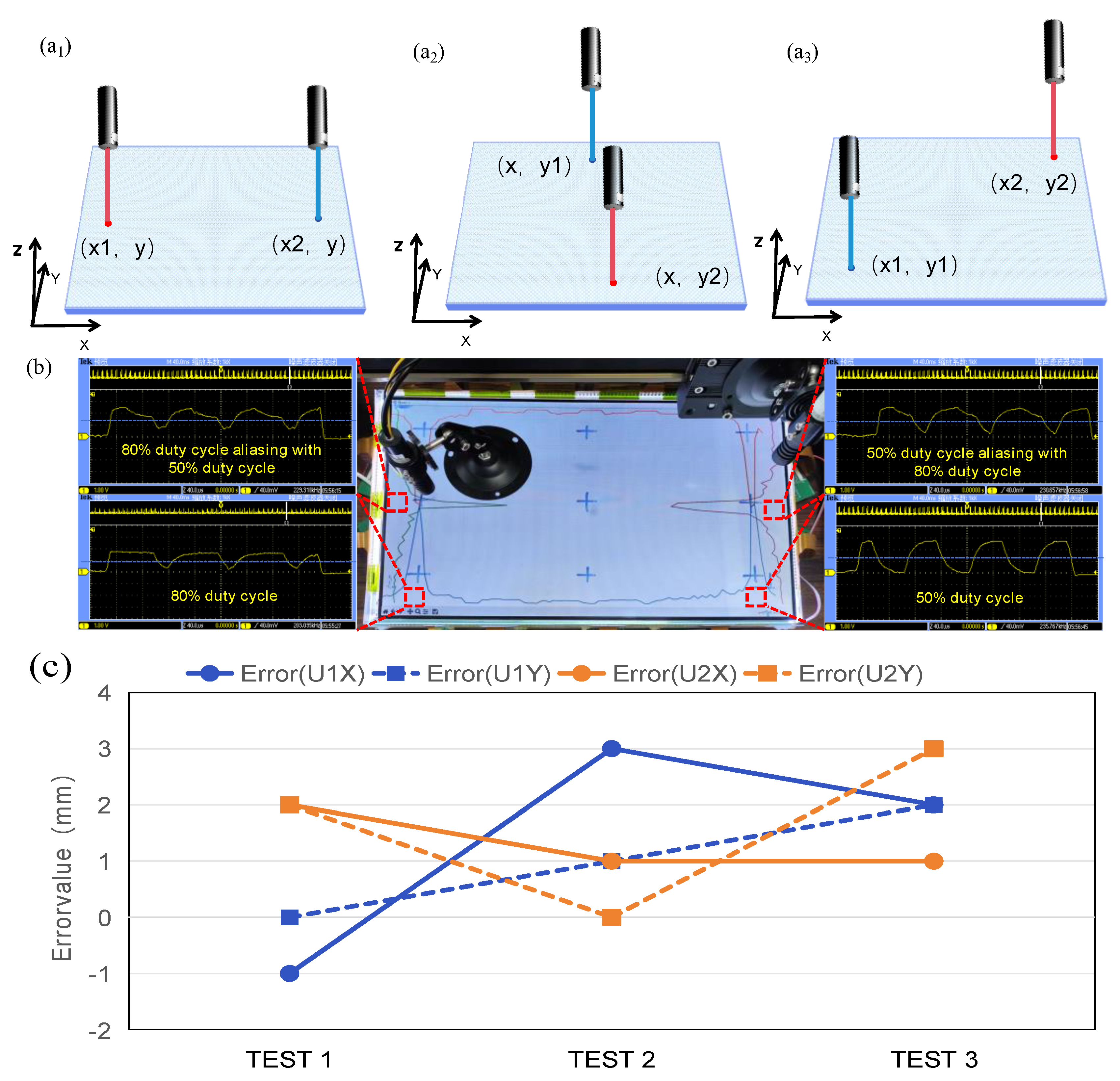
To demonstrate the viability of multi-user recognition, pluses with frequency of 10kHz and different duty cycle of 80% and 50% respectively were modulated on the twol incident infrared laser pointers,. As depicted in
Figure 10a, three types of positions for two-point incidence were considered: with the same Y coordinate, with the same X coordinate, and with both different X and Y coordinates.
A typical incidence corresponding to incident position of
Figure 10a1, is illustrated in
Figure 10b. Two laser pointers are aligned on the same y-axis, which results in a signal overlap area on the corresponding detector-arrays. Nevertheless, the conventional cross-lines intersection method merely based on unmodulated zero-frequency signals is unable to establish distinction between those inputs. While, the waveform at the peak voltage positions, as depicted in
Figure 10b, demonstrates that dynamic threshold judgment enables the differentiation of pulse width characteristics in the overlap area. Thus, the duty cycle detection is used to ascertain characteristics, allowing the drawing of intersecting lines at the voltage peak positions with the same characteristics to determine the unique interaction positions from the respective input. As shown in
Figure 10c, the matching discrepancy between the displayed user coordinates and the actual positions was within 3mm with satisfied accuracy for the entire experiment.
3.3. Interactive Performance Experiment
In the operation of optical touch systems, a user’s interaction trajectory is made up of discrete touch points, thus the spacing between these points significantly affects the fluidity of the interaction. To determine the response speed limits of the optical touch system, interactive performance experiments under single-point and two-point incidence conditions are conducted. In the single-point experiment, the screen was scanned by the laser along X-axis repeatedly at a speed of 0.5m/s, meanwhile the computed touch points were recorded and displayed on it. In the two-point experiment, another laser pointer with a different modulation characteristic was incorporated into the setup, while the rest processes remained unaltered. The scanning process was sustained for 20 seconds to facilitate a comprehensive assessment of the system’s continuity. The temporal intervals between accurately identified points served as indicators of the response times, whereas erroneously identified points were annotated for calculating the recognition accuracy.
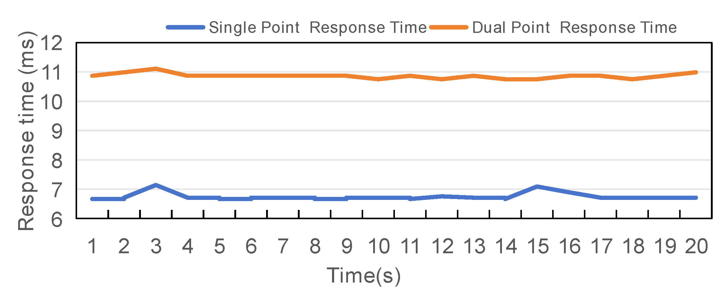
After single-point and dual-point experiments, the results of the response speed are shown in
Figure 11. Under single-point conditions, an average of 148 touches per second corresponding to a response time of 6.75ms per touch is observed. A total of 2963 touch points were displayed with just 17 misjudged points meaning a recognition accuracy of 99.4%.
In dual-point conditions, the display screen exhibited an average of 184 touch points per second for two users, i.e. 92 touch points per second for each user. This corresponds to a response time of approximately 10.8ms per touch. During the whole process, a total of 3682 touch points was displayed with just 17 misjudged points, resulting in a recognition accuracy of 99.5%. These results demonstrate that DCD’s performance approaches the perceptible latency threshold of 6ms [
20], thereby it satisfies the requirements for user interaction.
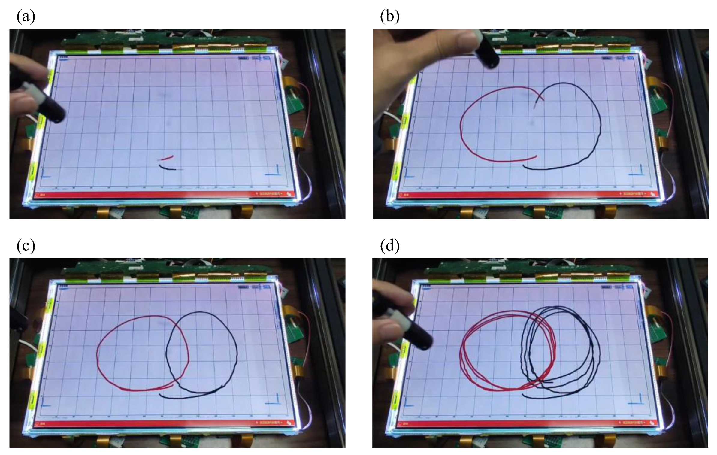
To demonstrate the inevitable crossover incidents inherent in multi-point input process, two laser pointers were utilized to draw intersecting circles on the screen. The writing demonstration with dual-point input is presented in
Figure 12. The input process comprises four states: initialization point recognition, intersection point identification, reversibility, and replicability. In the starting time, as shown in
Figure 12(a), we began by drawing circles from the bottom of the screen, with the starting points of the two laser pointers identifiable as red and black. At the intersecting moment, as shown in
Figure 12(b), the circles drawn by the two laser pointers of different colors intersect with each other, and the intersection points are correctly displayed in the respective corresponding color. At the returning state, as shown in
Figure 12(c), we have completed the drawing of two circular trajectories, and both trajectories are displayed independently without confusion. To ensure the reproducibility of the experiment, we repeated the drawing of intersecting circles with the two colors several times, as shown in
Figure 12(d). The experimental results indicate that DCD can identify crossover effects during operation, confirming the feasibility of multi-input interaction.
4. Conclusions
We proposed a differential amplitude modulation scheme for grating-antenna-based remote multi-point touch, where the grating antenna acting as the signal transmission media. To facilitate simultaneous multi-users interaction purpose, amplitude modulation upon incident beam is employed to identify the different users. For minimising distortion impacts and precisely demodulating of the signals and, the modulation period and pulse width were adjusted to match the electric character of the detectors during signal conversion. The scheme was successfully validated on an 18-inch screen, where concurrent two-point optical touch identification is achieved with a location recognition error under 3mm and a response time less than 7ms, yielding user-recognition accuracy exceeding 99.5%. In a word, our optical remote multi-touch technology opens a new way for future intelligent interaction, and we believe by using photodetectors with shorter response times or faster sampling chips, the response time of the interaction can by improve much better which can bring about fabulous experience to the users.
Author Contributions
Conceptualization, Y.H. and Y.W.; methodology, Y.H. and Y.W.; software, Y.H. and P.W.; validation, Y.H., W.L. and Z.G.; investigation, Y.H. and P.H.; data curation, Y.H. and Z.G.; Funding acquisition, Z.Y.; writing—original draft preparation, Y.H. and Z.Y.; writing —review and editing, Y.H. and Z.Y. All authors have read and agreed to the published version of the manuscript.
Funding
This research was funded by the Science Foundation of the Fujian Province, grant number 2023J01234 and Fujian Science & Technology Innovation Laboratory for Optoelectronic Information of China, grant number 2022ZZ202.
Institutional Review Board Statement
Not applicable.
Informed Consent Statement
Not applicable.
Data Availability Statement
The raw data supporting the conclusions of this article will be made available by the authors on request.
Conflicts of Interest
The authors declare no conflicts of interest.
References
- Ren, X.; Silpasuwanchai, C.; Cahill, J. Human-engaged computing: the future of human–computer interaction. CCF transactions on pervasive computing and interaction 2019, 1, 47–68. [Google Scholar] [CrossRef]
- Kotian, A. L.; Nandipi, R.; Ushag, M.; Veena, G. In A Systematic Review on Human and Computer Interaction, 2024 2nd International Conference on Intelligent Data Communication Technologies and Internet of Things (IDCIoT), 2024; IEEE: 2024; pp. 1214–1218.
- Barrett, G.; Omote, R. Projected-capacitive touch technology. Information Display 2010, 26, 16–21. [Google Scholar] [CrossRef]
- Calpe-Maravilla, J.; Medina, I.; Martinez, M. J.; Carbajo, A. In Dual touch and gesture recognition in 4-wire resistive touchscreens, SENSORS, 2014 IEEE, 2014; IEEE: 2014; pp 787-790.
- Mandal, D.; Banerjee, S. Surface acoustic wave (SAW) sensors: Physics, materials, and applications. Sensors 2022, 22, 820. [Google Scholar] [CrossRef] [PubMed]
- Maxwell, I. An overview of optical-touch technologies. Information Display 2007, 23, 26. [Google Scholar]
- Lee, S.; Nam, G. J.; Chae, J.; Kim, H.; Drake, A. J. Two-dimensional position detection system with MEMS accelerometers, readout circuitry, and microprocessor for padless mouse applications. Ieee Transactions on Very Large Scale Integration (Vlsi) Systems 2005, 13, 1167–1178. [Google Scholar]
- Eom, G.-M.; Kim, K.-S.; Kim, C.-S.; Lee, J.; Chung, S.-C.; Lee, B.; Higa, H.; Furuse, N.; Futami, R.; Watanabe, T. Gyro-mouse for the disabled: 'Click' and 'position' control of the mouse cursor. International Journal of Control Automation and Systems 2007, 5, 147–154. [Google Scholar]
- Wu, J.; Jafari, R. Orientation Independent Activity/Gesture Recognition Using Wearable Motion Sensors. Ieee Internet of Things Journal 2019, 6, 1427–1437. [Google Scholar] [CrossRef]
- Wang, Z.; Li, Y.; Jin, B.; Wang, Q.; Feng, Y.; Li, Y.; Shao, H. AirMouse: Turning a Pair of Glasses Into a Mouse in the Air. Ieee Internet of Things Journal 2019, 6, 7473–7483. [Google Scholar] [CrossRef]
- Capin, T.; Haro, A.; Setlur, V.; Wilkinson, S. In Camera-based virtual environment interaction on mobile devices, 21st International Symposium on Computer and Information Sciences (ISCIS 2006), Istanbul, TURKEY, 2006 Nov 01-03, 2006; Istanbul, TURKEY, 2006; pp. 765–773.
- Yousefi, S.; Kondori, F. A.; Li, H. CAMERA-BASED GESTURE TRACKING FOR 3D INTERACTION BEHIND MOBILE DEVICES. International Journal of Pattern Recognition and Artificial Intelligence 2012, 26. [Google Scholar] [CrossRef]
- Banerjee, A.; Burstyn, J.; Girouard, A.; Vertegaal, R. MultiPoint: Comparing laser and manual pointing as remote input in large display interactions. International Journal of Human-Computer Studies 2012, 70, 690–702. [Google Scholar] [CrossRef]
- Wada, T.; Takahashi, M.; Kagawa, K.; Ohta, J.; Ieee In Laser pointer as a mouse, Annual Conference on the Society-of-Instrument-and-Control-Engineers, Kagawa Univ, Takamatsu, JAPAN, 2007 Sep 17-20, 2007; Kagawa Univ, Takamatsu, JAPAN, 2007; pp. 366–372.
- Den Boer, W.; Abileah, A.; Green, P.; Larsson, T.; Robinson, S.; Nguyen, T. In 56.3: Active matrix LCD with integrated optical touch screen, SID Symposium Digest of Technical Papers, 2003; Wiley Online Library: 2003; pp. 1494–1497.
- Ting, C.-H.; Jen, T.-H.; Chen, C.-H.; Shieh, H.-P. D.; Huang, Y.-P. 3D Air-Touch User Interface With High Touch Accuracy on Stereoscopic Displays. Journal of Display Technology 2016, 12, 429–434. [Google Scholar] [CrossRef]
- Pasquariello, D.; Vissenberg, M. C. J. A.; Destura, G. J. Remote-touch: A laser input user-display interaction technology. Journal of Display Technology 2008, 4, 39–46. [Google Scholar] [CrossRef]
- Chengliang, W.; Haoyu, W.; Yifei, F.; Huiling, R.; Xinran, H.; Bisheng, W.; Shuai, J.; Jun, Z.; Zhicheng, Y. Optical human-machine interaction based on sub-wavelength gratings. SID Symposium Digest of Technical Papers 2019, 50 (suppl. S1), 1025–1025. [Google Scholar]
- Bodas, D.; Khan-Malek, C. Hydrophilization and hydrophobic recovery of PDMS by oxygen plasma and chemical treatment - An SEM investigation. Sensors and Actuators B-Chemical 2007, 123, 368–373. [Google Scholar] [CrossRef]
- Ng, A.; Lepinski, J.; Wigdor, D.; Sanders, S.; Dietz, P.; Acm In Designing for Low-Latency Direct-Touch Input, 25th Annual ACM Symposium on User Interface Software and Technology (UIST), Cambridge, MA, 2012 Oct 07-10, 2012; Cambridge, MA, 2012; pp. 453–464.
Figure 1.
Schematic diagram of the multi-point optical interaction system. The pulse signals with different width are modulated on the infrared lasers respectively.
Figure 1.
Schematic diagram of the multi-point optical interaction system. The pulse signals with different width are modulated on the infrared lasers respectively.
Figure 2.
Light transmission in the grating antenna layer diagram. The incident light from free space is coupled by the grating antenna, then it is converted to the confined light propagating along the waveguide, finally it is captured by the photodetectors positioned around the screens.
Figure 2.
Light transmission in the grating antenna layer diagram. The incident light from free space is coupled by the grating antenna, then it is converted to the confined light propagating along the waveguide, finally it is captured by the photodetectors positioned around the screens.
Figure 3.
(a) Schematic diagram of the structure of the grating antenna and waveguide. (b) Variation of the +1-order diffraction efficiency with incident wavelengths ranging from 350nm to 1200nm for grating periods of 600-1000nm.
Figure 3.
(a) Schematic diagram of the structure of the grating antenna and waveguide. (b) Variation of the +1-order diffraction efficiency with incident wavelengths ranging from 350nm to 1200nm for grating periods of 600-1000nm.
Figure 4.
The diagram of hardware components and layout of the optical touch system prototype. It includes an LCD panel, two layer of optical waveguide films, a backlight module, detector arrays, electronic signal circuit, and a microcontroller unit.
Figure 4.
The diagram of hardware components and layout of the optical touch system prototype. It includes an LCD panel, two layer of optical waveguide films, a backlight module, detector arrays, electronic signal circuit, and a microcontroller unit.
Figure 5.
(a)The set-up of a detector unit which consisting of a phototransistor, a Schottky diode, and a sampling resistor. (b) The working process of how the grating antenna-based position recognition module to obtain the incident positions and display them on the screen, which including signal scanning of detector arrays, environmental light calibration, peak voltage positions calculation, feature identification and interaction points display.
Figure 6.
The diagram of how the signals are transmitted in the optical touch system. The periodic fluctuations in the laser amplitude, linked to the PWM signal, are transformed into digital voltage signals through sampling the detection circuit. Then, the digital voltage signals are converted into Boolean values through dynamic threshold judgment and are classified by rising and falling edges to demodulate pulse width and frequency characteristics.
Figure 7.
Distortion analysis of signal demodulation. The sum effect of the prolonged rising and falling time can result in pulse stretching or compression, leading to signal distortion.
Figure 7.
Distortion analysis of signal demodulation. The sum effect of the prolonged rising and falling time can result in pulse stretching or compression, leading to signal distortion.
Figure 8.
The experimental setup of optical touch system which consists of three movable rails, a laser pointer, a display screen, and a detector array. A laser pointer fixed on one of the Y-directional rails can scan the entire screen by moving the X or Y rails.
Figure 8.
The experimental setup of optical touch system which consists of three movable rails, a laser pointer, a display screen, and a detector array. A laser pointer fixed on one of the Y-directional rails can scan the entire screen by moving the X or Y rails.
Figure 9.
The diagram of single-input experiments. (a) 9-point measurement schematic for evaluating position detection accuracy. (b) Response values of the sensor array when laser pointer is illuminated to position of No. 5. (c) Error evaluation of single input experiment.
Figure 9.
The diagram of single-input experiments. (a) 9-point measurement schematic for evaluating position detection accuracy. (b) Response values of the sensor array when laser pointer is illuminated to position of No. 5. (c) Error evaluation of single input experiment.
Figure 10.
Two-point touch error measurements, including (a1) the same Y, (a2) the same X, and (a3) different X and Y coordinates. (b)The response values of the sensor array when the laser pointer is illuminated as shown in Figure(a1). (c)Error evaluation of dual input experiment.
Figure 10.
Two-point touch error measurements, including (a1) the same Y, (a2) the same X, and (a3) different X and Y coordinates. (b)The response values of the sensor array when the laser pointer is illuminated as shown in Figure(a1). (c)Error evaluation of dual input experiment.
Figure 11.
Comparative analysis of DCD method in single-point and dual-point scenarios with response time.
Figure 11.
Comparative analysis of DCD method in single-point and dual-point scenarios with response time.
Figure 12.
Demonstration of simultaneous dual-point writing. Two laser pointers were utilized to draw intersecting circles on the screen, with the display reflecting the recognition outcomes. The process is divided into four stages of (a) starting, (b) intersecting, (c) returning, and (d) repeating.
|
Disclaimer/Publisher’s Note: The statements, opinions and data contained in all publications are solely those of the individual author(s) and contributor(s) and not of MDPI and/or the editor(s). MDPI and/or the editor(s) disclaim responsibility for any injury to people or property resulting from any ideas, methods, instructions or products referred to in the content. |
© 2024 by the authors. Licensee MDPI, Basel, Switzerland. This article is an open access article distributed under the terms and conditions of the Creative Commons Attribution (CC BY) license (http://creativecommons.org/licenses/by/4.0/).
