Submitted:
29 May 2024
Posted:
30 May 2024
You are already at the latest version
Abstract
Keywords:
1. Introduction
2. Materials and Methods
3. Results and Discussion
3.1. X-ray Results
3.2. Microstructure Analysis
3.3. XPS Results
3.4. Optical Results
3.5. Current-Voltage Characteristics

3.6. Direct Current Conductivity Results

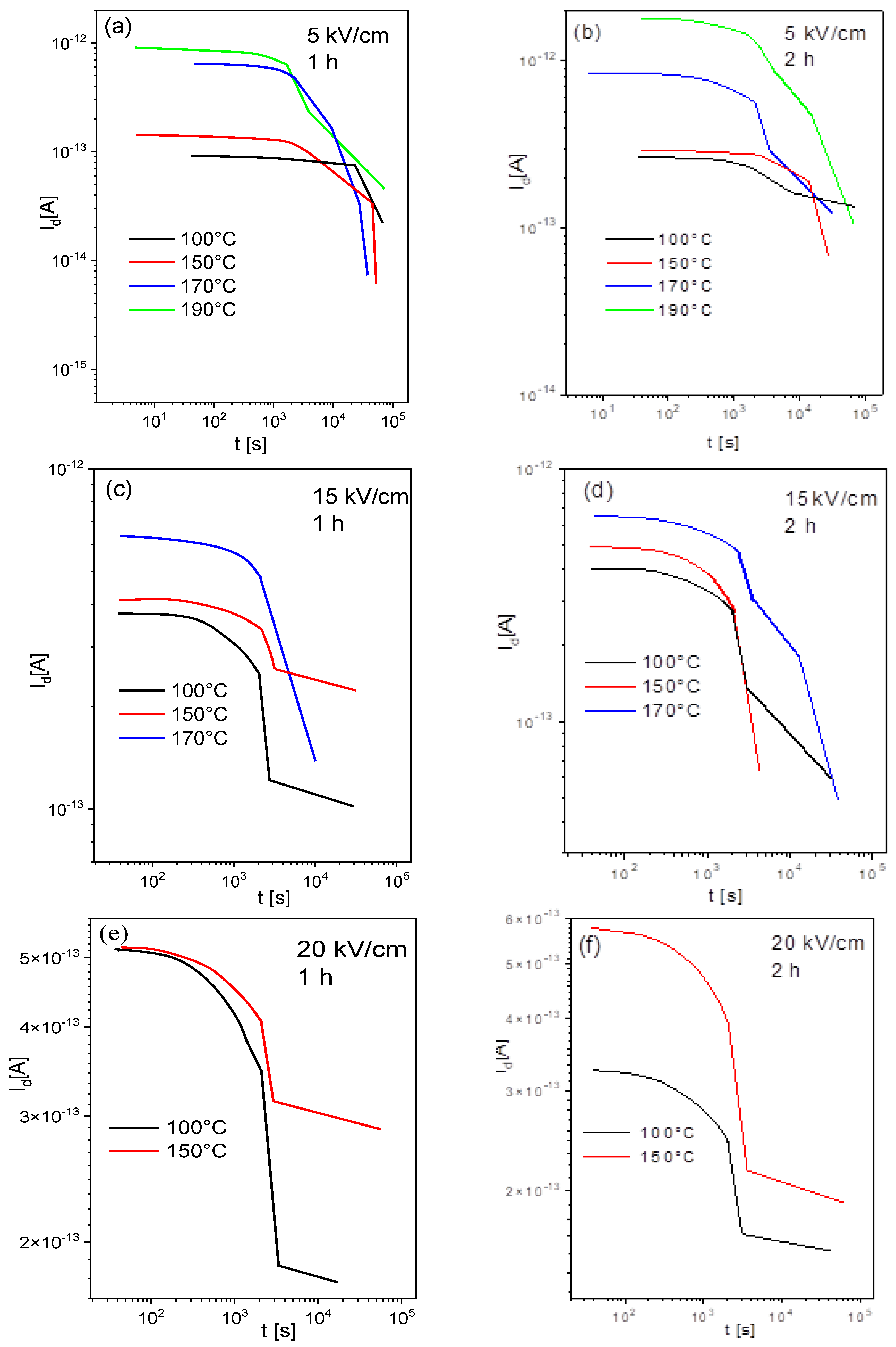
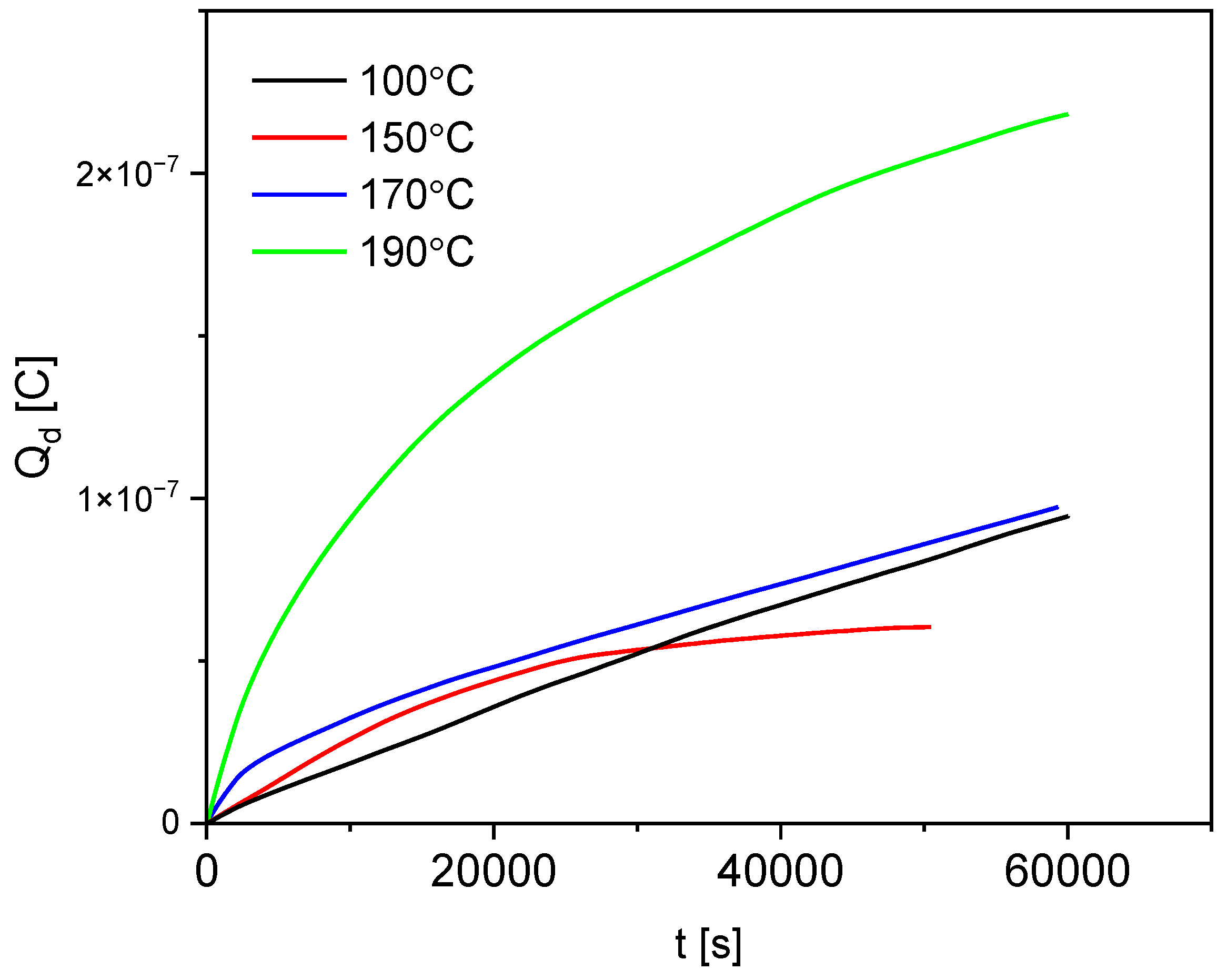
3.7. Depolarization Current Results
3.8. Alternating Current Conductivity Results
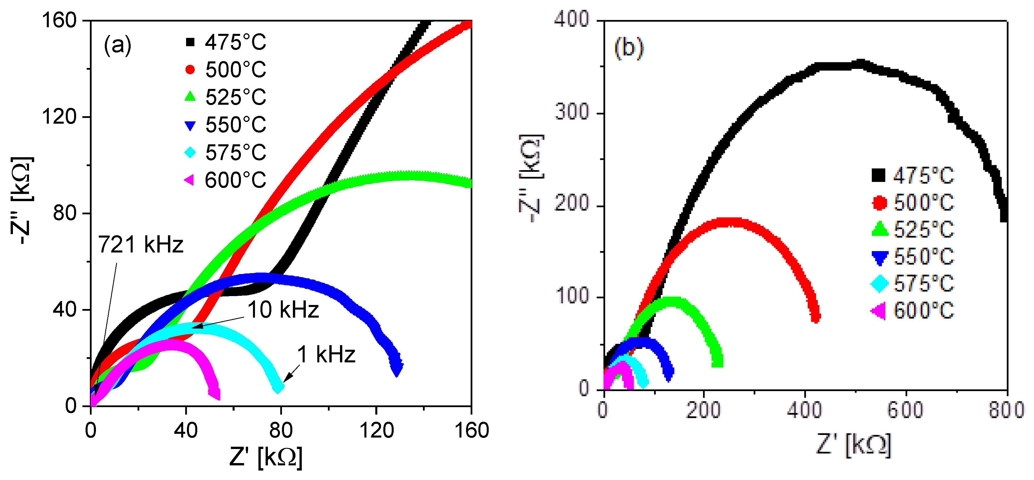
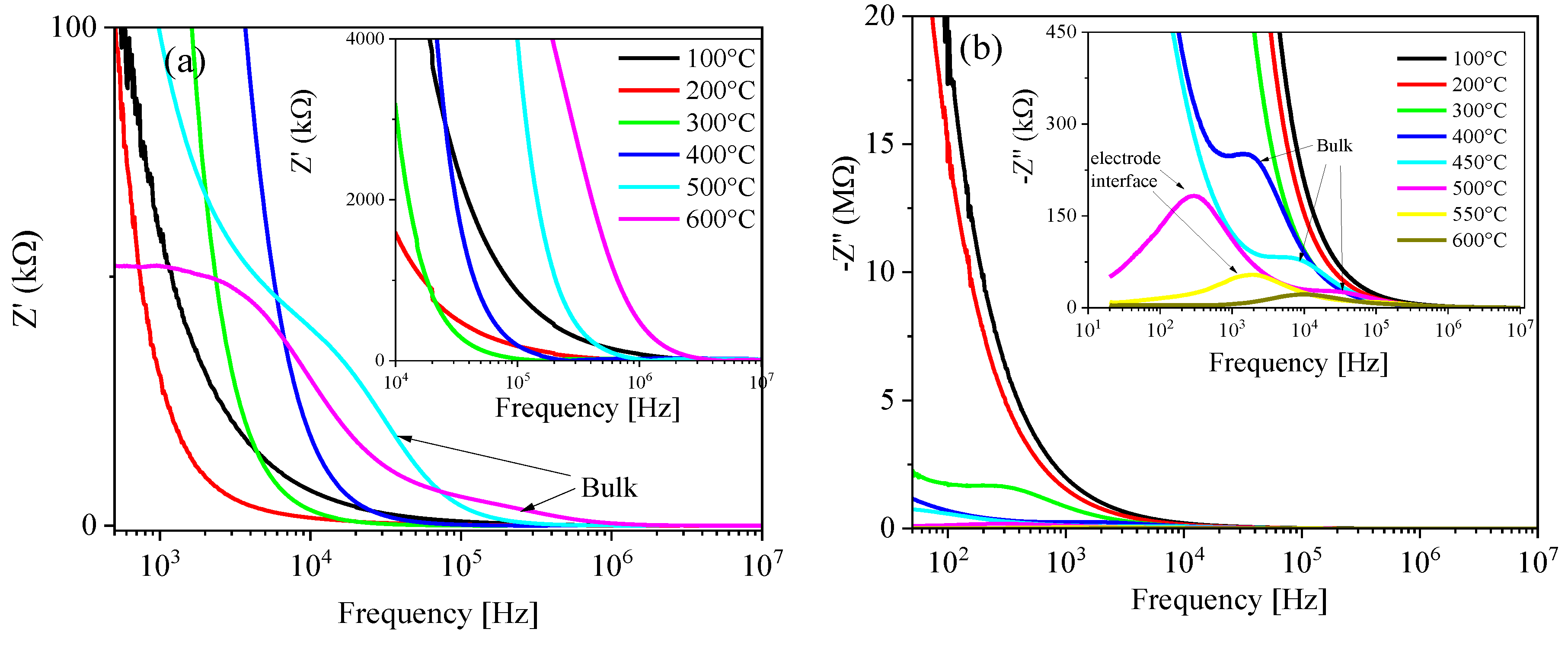
3.9. Complex Impedance Spectroscopy Analysis
3.10. Thermoelectric Results
1.11. Thermal Conductivity Results
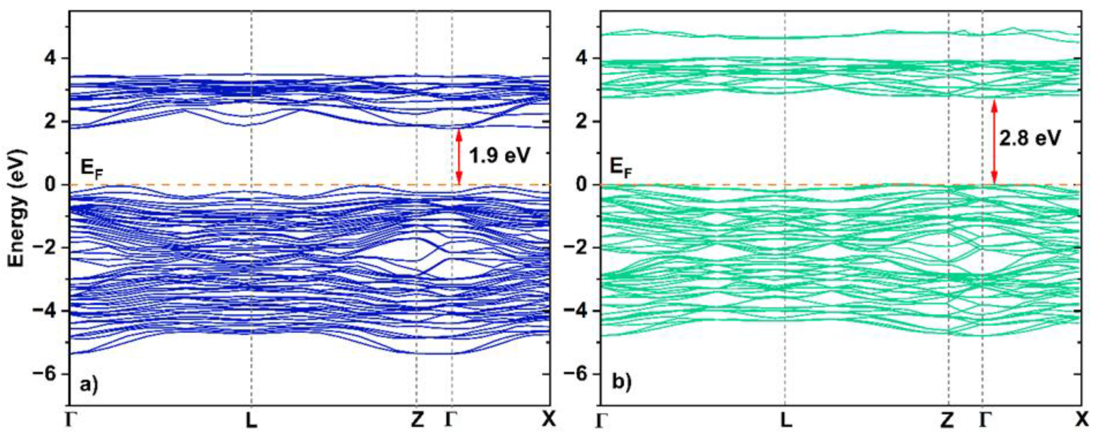
3.12. Ab Initio Calculations

4. Conclusions
Acknowledgments
References
- Uchino K. Ferroelectric devices. New York, NY: Marcel Dekker; 2000.
- Zachariasz R, Bochenek D. Properties of the PZT type ceramics admixed with barium and niobium. Archives of Metallurgy and Materials. 2009; 54:895-902.
- Skulski R, Wawrzała P, Ćwikiel K, Bochenek D. Dielectric and electromechanical behaviors of PMN-PT ceramic samples. Journal of Intelligent Material Systems and Structures. 2007;18: 1049-1056. [CrossRef]
- Bochenek D. Magnetic and ferroelectric properties of PbFe1/2Nb1/2O3 synthesized by solution precipitation method. J.Alloys. Comp. 2010;504:508-513. [CrossRef]
- Suchanicz J, Kluczewska K, Czaja P, Kania A, Konieczny K, Handke B, Sokolowski M, Trubitsyn MP, Kruzina TV. Structural, thermal, dielectric and ferroelectric properties of poled Na0.5Bi0.5TiO3 ceramics. Ceramics International. 2017;43:17194-17201.
- Aksel E, Forrester JS, Jones JL, Thomas PA, Page K, Suchomel MR. Monoclinic crystal structure of polycrystalline Na0.5Bi0.5TiO3. Appl. Phys. Lett. 2011; 98: 152901 (1-5). [CrossRef]
- Rao BN, Fitch AN, Ranjan R. Ferroelectric-ferroelectric phase coexistence in Na1/2Bi1/2TiO3. Phys. Rev. 2013; B87: 060102 (1-8). [CrossRef]
- Dorcet V, Trolliard G, Boullay P. Reinvestigation of phase transitions in Na0.5Bi0.5TiO3 by TEM. Part I: First order rhombohedral to orthorhombic phase transition. Chem. Mater. 2008; 20: 5061-5073. [CrossRef]
- Trolliard G, Dorcet V. Reinvestigation of phase transitions in Na0.5Bi0.5TiO3 by TEM.Part II: Second order orthorhombic to tetragonal phase transition. Chem. Mater. 2008; 20: 5074-5082. [CrossRef]
- Aktas O, Duclere JR, Quignon S, Trolliard SG, Salje EKH. Polarity of modulated Na0.5Bi0.5TiO3 and its slow structural relaxation. Appl. Phys. Lett. 2018; 113: 032901(1-4). [CrossRef]
- Suchanicz J. Behaviour of Na0.5Bi0.5TiO3 ceramics in the ac electric field. Ferroelectrics. 1998;209:561-568. [CrossRef]
- Vakhrushev SB, Isupov VA, Kvyatkovsky BE, Okuneva NM, Pronin IP, Smolensky GA, Syrnikov PP. Phase transitions and soft modes in sodium bismuth titanate. Ferroelectrics.1985, 63: 153-160. [CrossRef]
- Suchanicz A, Roleder K, Kania A, Handerek J. Electrostrictive strain and pyroeffect in the region of phase coexistence in Na0.5Bi0.5TiO3. Ferroelectrics.1988; 77:107-110. [CrossRef]
- Suchanicz J. Elastic constants of Na0.5Bi0.5TiO3 single crystal. J.Mater.Sci. 2002; 37: 489-491. [CrossRef]
- Sakata K, Masuda Y. Ferroelectric and antiferroelectric properties of Na0.5Bi0.5TiO3-SrTiO3 solid solution ceramics. Ferroelectrics. 1974; 7, 347-349. [CrossRef]
- Aksel E, Forrester JS, Nino JC, Page K, Shoemaker P, Jones JL. Local atomic structure deviation from average structure of Na0.5Bi0.5TiO3: Combined x-ray and neutron total scattering study. Phys.Rev. 2013; B87:104113 (1-10). [CrossRef]
- Balagourov AM, Koroleva EY, Naberezhnov AA, Sakhnenko VP, Savenko BN, Ter-Oganessian AA, Vakhrushev SB. The rhombohedral phase with incommensurate modulation in Na0.5Bi0.5TiO3. Phase Transitions. 2006;79:163-173. [CrossRef]
- Barick BK, Mishra KK, Arora AK, Choudhary RNP, Pradhan DK. Impedance and Raman spectroscopic studies of Na0.5Bi0.5TiO3. J Phys D: Appl Phys. 2011;44:355402 (1-10). [CrossRef]
- East J, Sinclair DC. Characterization of (Bi1/2Na1/2)TiO3 using electric modulus spectroscopy. J Mater Sci. Lett. 1997;16:422-435. [CrossRef]
- Saradhi BVB, Srinivas K, Prasad G, Suryanarayana SV, Bhimasankaram T. Impedance spectroscopic studies in ferroelectric Na0.5Bi0.5TiO3. Mat. Sci. Eng. 2003;B98:10-16.
- Suchanicz J, Kluczewska-Chmielarz K, Sitko D, Jagło G. Electrical transport in lead-free Na0.5Bi0.5TiO3 ceramics. J.Adv.Ceram. 2021;10:152-156. [CrossRef]
- Karpierz M, Suchanicz J, Konieczny K, Smiga W, Czaja P, Sokolowski M. Effects of PbTiO3 doping on electric properties of Na0.5Bi0.5TiO3 ceramics. Phase Transitions. 2016;90:65-71. [CrossRef]
- Kresse G, Furthmüller J. Efficient iterative schemes for ab initio total-energy calculations using a planewave basis set. Phys. Rev. B. 1996;54:11169-11186. [CrossRef]
- Kresse G, Furthmüller J. Efficiency of ab initio total energy calculations for metals and semiconductors using a plane-wave basis set. Computational Materials Science. Mater. Sci. 1996; 6: 15-50. [CrossRef]
- Perdew JP, Burke K, Ernzerhof M. Generalized gradient approximation made simple. Phys. Rev. Lett. 1996; 77: 3865-3868. [CrossRef]
- Lü H, Wang S, Wang X. The electronic properties and lattice dynamics of Na0.5Bi0.5TiO3: From cubic to tetragonal and rhombohedral phases. J. Appl. Phys. 2014; 115: 124107(1-7). [CrossRef]
- Berri S. Ab initio study of fundamental properties of XAIO3 (X=Cs, Rb and K) compounds. J. Sci. Adv. Mater. Devices. 2018; 3: 254–261. [CrossRef]
- Mandal, B., Thakur, A.K. Electrode response of NaFeTiO4 in aqueous supercapacitor cells. Ionics. 2021;27:1709-1721. [CrossRef]
- Siddiqui TAJ, Shaikh SF, Sangale SS, Raut SD, Mane RS, Ubaidullah M, Thamer BM, Al-Enizi AM, Totawar BB, Samdani MS. Mesoporous carbon of carbonized human urine waste: a valuable heterogeneous catalyst for chromone and xanthene derivative synthesis. Catalysts. 2020;10:1369(1-17). [CrossRef]
- Cheng L, Hu X, Hao L. Easily recycled Bi2O3 photocatalyst coatings prepared viaball milling followed by calcination. Appl. Phys. A. 2017;123:443(1-7). [CrossRef]
- https://doi.org/10.1007/s00339-017-1051-x.
- Zhou Z, Xiong P, Liu H, Peng M. Ultraviolet a persistent luminescence of a Bi3+- activated LiScGeO4 material. Inorg. Chem. 2020;59:12920-12927. [CrossRef]
- Hou D, Hu X, Wen Y, Shan B, Hu P, Xiong X, Qiaoa Y, Huanga Y. Electrospun sillenite Bi12MO20 (M = Ti, Ge, Si) nanofibers: general synthesis, band structure, and photocatalytic activity. Phys. Chem. Chem. Phys. 2013;15:20698-20705. [CrossRef]
- Łapiński M. Czubek J. Drozdowska K. Synak A. Sadowski W. Kościelska B. Plasmon-enhanced photoluminescence from TiO2 and TeO2 thin films doped by Eu3+ for optoelectronic applications. Beilstein J. Nanotechnol. 2021;12:1271–1278. [CrossRef]
- Horvath H. Gustav Mie and the scattering and absorption of light by particles: Historic developments and basics. Journal of Quantitative Spectroscopy & Radiative Transfer. 2009;110:787–799. [CrossRef]
- Stern F. Elementary theory of the optical properties of solids. Solid State Phys.1963;15:299-408. [CrossRef]
- Li L, Li M, Zhang H, Reaney IM, Sinclair DC. Controlling mixed conductivity inNa1/2Bi1/2TiO3 using A-site non-stoichiometry and Nb-donor doping. J. Mater. Chem.C. 2016;4: 5779 (1-8). [CrossRef]
- Andriyevsky B, Suchanicz J, Cobet C, Patryn A, Esser N, Kosturek B. Manifestation of phase transformations in optical spectra of Na0.5Bi0.5TiO3 crystals between 25oC and 350oC. Phase Transitions. 2009;82:567–575. [CrossRef]
- Zeng M, Or SW, Chan HL. First – principles study on the electronic and optical properties of Na0,5Bi0.5TiO3 lead free piezoelectrical crystal. J.Appl. Phys. 2010;107: 043513(1-8). [CrossRef]
- Bousquet M, Duclère J-R, Orhan E, Boulle A, Bachelet C. Optical properties of anepitaxial Na0,5Bi0.5TiO3 thin film grown by laser ablation: Experimental approach and density functional theory calculations. J. Appl. Phys. 2010;107:104107 (1-9). [CrossRef]
- Scott JF, Araujo CA, Melnick BM, McMillan LD, Zuleeg R. Quantitative measurement of space-charge effects in lead zirconate-titanate memories. J. Appl. Phys. 1991;70:382–385. [CrossRef]
- Lampert MA. Simplified theory of space-charge-limited currents in an insulator with traps. Phys. Rev. 1956;103: 1648-1656. [CrossRef]
- Huey RM, Taylor R McK. Anomalous discharges in ferroelectrics, J. Appl. Phys. 1963;34:1557-1560. [CrossRef]
- Szot K, Bihlmayer G, Speier W. Nature of the resistive switching phenomena in TiO2 and SrTiO3: origin of the reversible /insulator-metal transition. Solid State Physics. 2014;65:354-544. [CrossRef]
- Stanuch K, Sitko D, Kruk A, Suchanicz J, Nowakowska-Malczyk M, Wąs M, Konieczny K, Czaja P, Kluczewska-Chmielarz K, Stachowski G, Bik M, Łyszczarz K, Sokolowski M. Effects of Sr dopant and electric field poling on structural, thermal and dielectric properties of Ba(1-x )SrxTiO3 ceramics (x = 0, 0.3, 0.4 and 0.45). Phase Transitions. 2022; 95:456-465. [CrossRef]
- Bharti C, Sen A, Sinha TP. Enhanced dielectric and ferroelectric properties of Ca2+substituted sodium bismuth titanate. AIP Conference Proceedings. 2013;1512:1306-1307. [CrossRef]
- He X, Mo Y. Accelerated materials design of Na0.5Bi0.5TiO3 oxygen ionic conductors based on first principles calculations. Phys. Chem. Chem. Phys. 2015;17:18035-18044. [CrossRef]
- Li M, Pietrowski MJ, De Souza RA, Zhang H, Reaney IM, Cook SN, Kilner JA, Sinclair DC. A family of oxide ion conductors based on the ferroelectric perovskite Na0.5Bi0.5TiO3. Nature Materials. 2014;13:31-35. [CrossRef] [PubMed]
- Schönleber M, Klotz D, Ivers-Tiffée E. A Method for improving the robustness of linear Kramers-Krönig validity tests. Electrochimica Acta. 2014;131:20-27. [CrossRef]
- Steinsvik S, Bugge R, Gjonnes J, Tafto J, Norby T. The defect structure of SrTi1−xFexO3−y (x = 0–0.8) investigated by electrical conductivity measurements and electron energy loss spectroscopy (EELS). J.Phys.Chem.Solids. 1997;58:969-976. [CrossRef]
- Alaka P, Govindaraj R. Complex dielectric and impedance spectroscopic studies in a multiferroic composite of Bi2Fe4O9-BiFeO3. Condes.Matter Phys. 2018;3:44(1-15). [CrossRef]
- Gillot C, Michenaud JP. Electrical conductivity of similarly doped BaTiO3 single crystal and ceramics in the rhombohedral phase. Solid State Com. 1994;90:23-25. [CrossRef]
- Chandra Sekhar KSKR, Mahesh MLV, Sreenivasu T, Rama Krishna Y, Chandra Mouli K, Patri Tirupathi P. Structural evolution, dielectric relaxation and modulus spectroscopic studies in Dy substituted NBT-BT ferroelectric ceramics. J.Mat.Sci. 2021;32:8628–8647. [CrossRef]
- Almond D, Duncan GK, West AR. The determination of hopping rates and carrier concentrations in ionic conductors by a new analysis of ac conductivity. Sold State Ionics.1983;8:159- 164. [CrossRef]
- Chen RH, Yen CC, Shen CS, Fukami T. Impedance spectroscopy and dielectric analysis in KH2PO4 single crystal. Solid State Ionics. 2006;177:2857- 2864. [CrossRef]
- Macdonald JR. Note on the parametrization of the constant-phase admittance element. Solid State Ionics. 1984;13:147-149. [CrossRef]
- Hajra S, Sahoo S, Das R, Choudhary RNP. Structural, dielectric and impedance characteristics of Na0.5Bi0.5TiO3–BaTiO3 electronic system. J.Alloys Comp. 2018;750:507-514. [CrossRef]
- Ang C, Yu Z, Cross LE. Oxygen-vacancy-related low-frequency dielectric relaxation and electrical conduction in Bi:SrTiO3. Phys.Rev. 2000;B62:228-236. [CrossRef]
- Saha S, Krupanidhi SB. Dielectric response in pulsed laser ablated (Ba, Sr)TiO3 thin films. J.Appl.Phys. 2000;87: 849–854. [CrossRef]
- Rani R, Sharma S, Rai R, Kholkin AL. Investigation of dielectric and electrical properties of Mn doped sodium potassium niobate ceramic system using impedance spectroscopy. J.Appl.Phys. 2011;110:104102 (1-12). [CrossRef]
- Raymond O, Font R, Suárez-Almodover N, Portelles J, Siqueiros M. Frequency-temperature response of ferroelectromagnetic Pb(Fe1/2Nb1/2)O3 ceramics obtained by different precursors. Part II. Impedance spectroscopy characterization. J.Appl.Phys. 2005;97:084108 (1-8). [CrossRef]
- Pradhan DK, Choudhary RNP, Rinaldi C, Katiyar RS. Effect of Mn substitution on electrical and magnetic properties of Bi0.9La0.1FeO3.. J.Appl.Phys. 2009;106:024102 (1-10). [CrossRef]
- Peláiz-Barranco A, González-Abreu Y, López-Noda R. Dielectric relaxation and conductivity behavior in modified lead titanate ferroelectric ceramics. J.Phys.Condens.Matter. 2008;20:505208 (1-10). [CrossRef]
- Kang BS, Choi SK, Park CH. Diffuse dielectric anomaly in perovskite-type ferroelectric oxides in the temperature range of 400–700 °C. J.Appl.Phys. 2003;94:1904-k 1911. [CrossRef]
- Singh G, Tiwari V, Gupta P. Role of oxygen vacancies on relaxation and conduction behavior of KNbO3 ceramic. J.Appl.Phys. 2010;107:064103 (1-8). [CrossRef]
- Liu L, Huang Y, Li Y, Wu M, Fang L, Hu C, Wang Y. Oxygen-vacancy-related high temperature dielectric relaxation and electrical conduction in 0.95K0.5Na0.5NbO3-0.05BaZrO3 ceramic. Physica B: Condensed Matter. 2012;407:136-139. [CrossRef]
- Erdem E, Jakes P, Eichel R-A, Sinclair DC, Pasha M, Reaney IM. Formation of (Ti’Ti-VOˑˑ) defect dipoles in BaTiO3 ceramics heat-treated under reduced oxygen partial-pressure. Funct.Mater.Lett. 2010;3:65-68. [CrossRef]
- Yang F, Li M, Li L, Wu P, Velázquez E, Sinclair DC. Defect chemistry and electrical properties of sodium bismuth titanate perovskite. J.Mater.Chem. 2018; A6:5243-5254. [CrossRef]
- Davson JA, Chen H, Tanaka I. Crystal structure, defect chemistry and oxygen ion transport of the ferroelectric perovskite Na0.5Bi0.5TiO3: insights from first-principles calculations. J.Mater.Chem. 2015;A3:16574-16582. [CrossRef]
- Cox TA. Transition metal oxides. Oxford (UK): Oxford University Press, 1992.
- Austin IG, Mott NF. Polarons in crystalline and non-crystalline materials. Adv Phys.1969;18:41-102. [CrossRef]
- Li M, Zhang H, Cook SN, Li L, Kilner JA, Reaney IM, Sinclair DC. Dramatic influence of A-site nonstoichiometry on the electrical conductivity and conduction mechanisms in the perovskite oxide Na0.5Bi0.5TiO3. Chem.Mater. 2015;27:629-634. [CrossRef]
- Suchanicz J, Nowakowska-Malczyk M, Kania A, Budziak A, Kluczewska-Chmielarz K, Czaja P, Sitko D, Sokolowski M, Niewiadomski A, Kruzina TV. Effect of electric field poling on structural, thermal, vibrational, dielectric and ferroelectric properties of Na0.5Bi0.5TiO3 single crystals. J.Alloys Comp.2021; 854: 157227 (1-17). [CrossRef]
- Suchanicz J, Kwapulinski J. X-ray diffraction study of the phase transitions in Na0.5Bi0.5TiO3. Ferroelectrics. 1995;165:249-253. [CrossRef]
- Zvirgzds JA, Kapostins PP, Zvirgzde JV,Kruzina TV. X-ray study of phase transitions in ferroelectric Na0.5Bi0.5TiO3. Ferroelectrics. 1982;40:75-77. [CrossRef]
- Min Zeng, Siu Wing Or, and Helen Lai Wa Chan. First-principles study on the electronic and optical properties of Na0.5Bi0.5TiO3 lead-free piezoelectric crystal. J.Appl.Phys. 2010; 107: 043513; [CrossRef]




Disclaimer/Publisher’s Note: The statements, opinions and data contained in all publications are solely those of the individual author(s) and contributor(s) and not of MDPI and/or the editor(s). MDPI and/or the editor(s) disclaim responsibility for any injury to people or property resulting from any ideas, methods, instructions or products referred to in the content. |
© 2024 by the authors. Licensee MDPI, Basel, Switzerland. This article is an open access article distributed under the terms and conditions of the Creative Commons Attribution (CC BY) license (http://creativecommons.org/licenses/by/4.0/).


