1. Introduction – FR3 Use for eMMB via Analog Beamformers
It is anticipated that the mid band spectrum FR3 (spectrum between FR1 and FR2) would be the Urban Extreme Capacity for 6G, [
1,
2]. A simple examination of the 5G occupied bands shows that the FR3 band is the only one left for enhanced Mobile Brodaband (eMMB) use and, thus, it has an enormous potential in terms of coverage and capacity. This frequency band facilitates co-deployment, enabling 5G, advanced 5G, and 6G cellular infrastructure to operate at the same cell sites, thereby minimizing deployment costs to practically zero. While the eMBB demands significant increase in Capacity, Throughput and Spectral Efficiency, massive multiple-input-multiple-output (MIMO) or GIGA MIMO will be the key enabling technologies for the realization of advanced 5G and 6G wireless communication, [
3,
4]. Massive MIMO exploits the advantages of beamforming technologies to enhance the efficiency of wireless communication. To fulfill the requirements of modern wireless systems, the deployment of multibeam antenna arrays, employing either passive beamforming with fixed beams or active beamforming with flexible beams, emerges as the optimal solution. Thus, the essential part of multibeam antenna arrays is the beamforming network (BFN), which in general, is classified into digital BFN, [
5], analogue BFN, [
6] and the combination of two as hybrid BFN, [
7]. Analogue BFNs, compared to digital BFNs are cost effective more energy-efficient and preferable in large-scale applications due to their simplicity, [
8].
Popular analogue BFNs or RF-type BFNs are Blass [
9], Nolen [
10] and Butler Matrix (BM), [
11]. BMs are the most widely used BFNs for feeding antenna arrays due to their easy fabrication, low cost and low profile [
12] and they may offer Ultra-Wideband (UWB) characteristics given certain topologies.
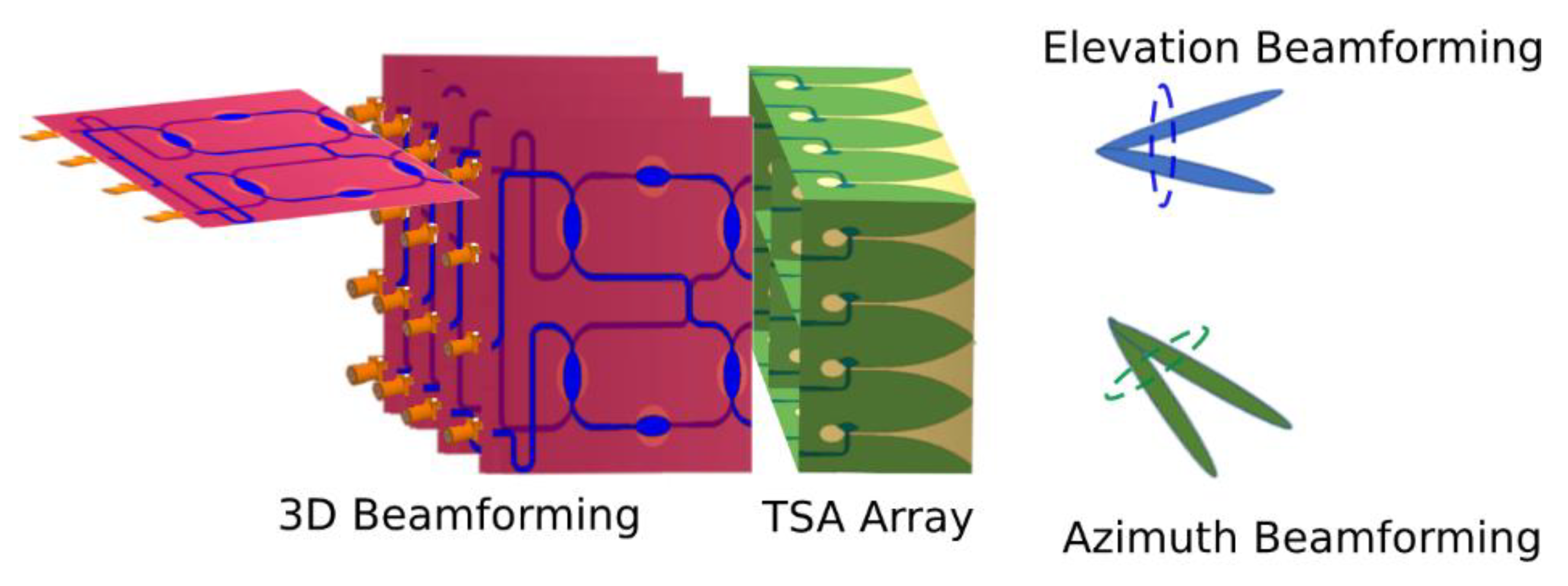
Figure 1 depicts an example of a 3D beamforming topology which could increase the capacity and efficiency of a system, supporting both transmit and receive functions with narrow beams in both azimuth and elevation angles. The analog three dimensional beamformer is build using a stack of vertical BMs driven by either a single or a stack of horizontal BMs. Ultra-wideband planar printed Vivaldi antenna elements are forming the planar array. It is clear from the above discussion that to deliver a fully functional and efficient BFN for currently anticipated 6G enhanced mobile broadband use case, we need to develop an UWB system covering the 7-24GHz band. Moreover, the RF-BFN, the BM in our case should be of compact size with UWB characteristics providing fixed radiation pattern through amplitude and phase accuracy. Thus, the miniaturization of the BM, while preserving or achieving the needed performance, is the most critical point for the realization of a multibeam antenna array similar to that of
Figure 1.
Numerous miniaturization efforts for the BM are reported in the literature and reviewed next. The recent advancements in 4×4 BM are summarized in
Table 1 and those of 8×8 BM are depicted in
Table 2. These approaches are grouped into single-layer (SL) [
13,
14,
15,
16,
17,
18,
19] and multilayer (ML) [
20,
21,
22,
23,
24,
25,
26,
27,
28,
29] configurations. In [
13,
14] artificial transmission line branch line coupler (BLC) and swapped ports coupled line coupler, respectively, are utilized to achieve a reduction in the size of the BM from 21% to 10% (0.11λ
2 – 0.05 λ
2) when compared to the conventional BM, while maintaining a fractional bandwidth (FBW) of 30%. In [
15,
16,
17], elimination of phase shifter and crossovers approach is enforced, using 45° and 90° couplers only, to build the BM. Therein, an improvement on the FBW is reported (45% - 63%) with miniaturized sizes ranging from 1.41
-1.22
. While works [
13,
14,
15,
16,
17] refer to 4×4 BM, in [
18] a conventional 8×8 BLC BM, printed in glass substrate was presented with narrow FWB of 2.6% and large size of 33.5
. Nevertheless in [
19] two asymmetrical 4×4 BMs consisting of BLCs are employed to form an 8×8 BM with reduced size of 4.14
and FBW equal to 24%.
Regarding multilayer configurations, a folded 4×4 BM with eliminated crossovers couplers was newly proposed in [
20]. Stacking half components of the BM on different layers, while combining them with multilayer transition scheme achieved a Footprint Area (FA) of 7.67
and an FBW of 14%. Similar FBW is achieved in [
21] where the components of a conventional 4×4 BM are stacked up in four different layers using the low temperature co-fired ceramics (LTCC) process, thus achieving significantly reduced size with FA of 1.12
. An increase in the FBW to 26.5% is reported in [
22], adopting the grounded coplanar waveguide (GCPW) technology. Using bent hybrid couplers, curved line phase shifter and multilayer transitioned crossovers, a size with FA of 5.04
is obtained. A good compromise between size and BW is reported in [
23,
24]. In [
23] a BM composed of forward wave directional couplers (FWDC) combined with microstrip line phase shifters and via crossovers, is proposed, resulting in a compact size of 1.19
and FBW of 47%. In [
24], dual transmission line couplers and circular patched phase shifters combined with elliptic and circular slots respectively, resulted in a compact BM with FA of 0.78
and FBW of 40%. Concerning 8×8 BM designs, slot-line transition and magic tees are utilized in [
25], where a 8×8 BM with 3 dB 180° couplers and several phase shifters (PS) is proposed. The achieved FBW is 60% and FA equal to 15.04
. A conventional 8×8 BM comprised of BLCs and Schiffman phase shifters is proposed in [
26]. The multilayered configuration is achieved using vias to connect the components at different layers, achieving size with FA of 4.4
and a FBW of 32%. Stripline technology is employed in [
27,
28,
29] for the implementation of compact 8×8 BMs. Specifically, in [
27], two 4×4 BM using both 90° and 180° couplers combined with an output network of the same couplers and several different PSs are proposed. Despite the reduced number of crossovers, the inclusion of output network and multiple PSs increase the complexity of the proposed design and the size (FA=2.56
), while the FBW is only 5.5%. In [
28], an 8×8 BM composed of coupled line quadrature directional couplers and coupled line Schiffman C-sections PS is proposed. The designs feature reduced number of crossovers and thus the obtained size is 2.46
and a significantly enhanced FBW of 73% is achieved. An optimal trade-off between BW and size is reported in [
29]. Therein, a 8×8 BM with single section 3 dB/90° directional couplers and PSs realized in tandem connection of two 3 dB/90° coupler, is proposed. The achieved size is 1.3
and FBW of 66%.
In this paper we propose two different design approaches for the BM beamformers, targeting the FR-3 band and utilizing the microstrip to slot technology. The BMs are realized using multilayer 3 dB/90° hybrid couplers (HC) and PS with elliptical geometry. The first design approach focuses on designing the components comprising the BM (HC, PS, etc.) separately and then integrating them to form the overall BM structure. Thus, an 8×8 BM operating in the 6 GHz – 16 GHz band was successfully designed and prototyped. Except the UWB characteristics where an FBW of 92% were achieved, a compact size was delivered, replacing the reference microstrip lines associated with the PSs and required for the appropriate differential phase, with meander lines (ML). The second method introduces a novel design approach utilizing the wideband matching technique. This technique simplifies the implementation process by designing the BM as a single, unified structure and contributes to further reduction of the size of the BM while maintaining the same and even higher FBW. For this case, a 4×4 and 8×8 BMs, were successfully implemented and simulated for the FR3 band, achieving compact size and UWB operation while meeting the desired performance criteria.
Table 1 and 2 provide a comprehensive summary of the performance metrics for the mentioned multilayer designs concerning the 4×4 and 8×8 BMs respectively. Therein, except the size and FBW, various characteristics including technology, amplitude imbalance and phase accuracy are listed in comparison with the herein contributed designs.
As shown from
Table 1 and
Table 2, our proposed designs exhibit the best performance in terms of BW and offer comparable size with the reported works. Concerning the phase accuracy, the deviation listed especially in
Table 2, is expected given the large BW of operation. Notably, our proposed BM topologies integrate an equiphased transmission line (TL) network leading in a significant increase in the overall size of the BMs. The size of the BMs alone (excluding the TL network) is provided in parenthesis in
Table 2 for clarity.
The rest of the paper is organized as follows:
Section 2 demonstrates the BM design methods, while
Section 3 presents the results of the implemented and prototyped designs. Finally,
Section 4 draws conclusions regarding the proposed work.
2. Butler Matrix Design
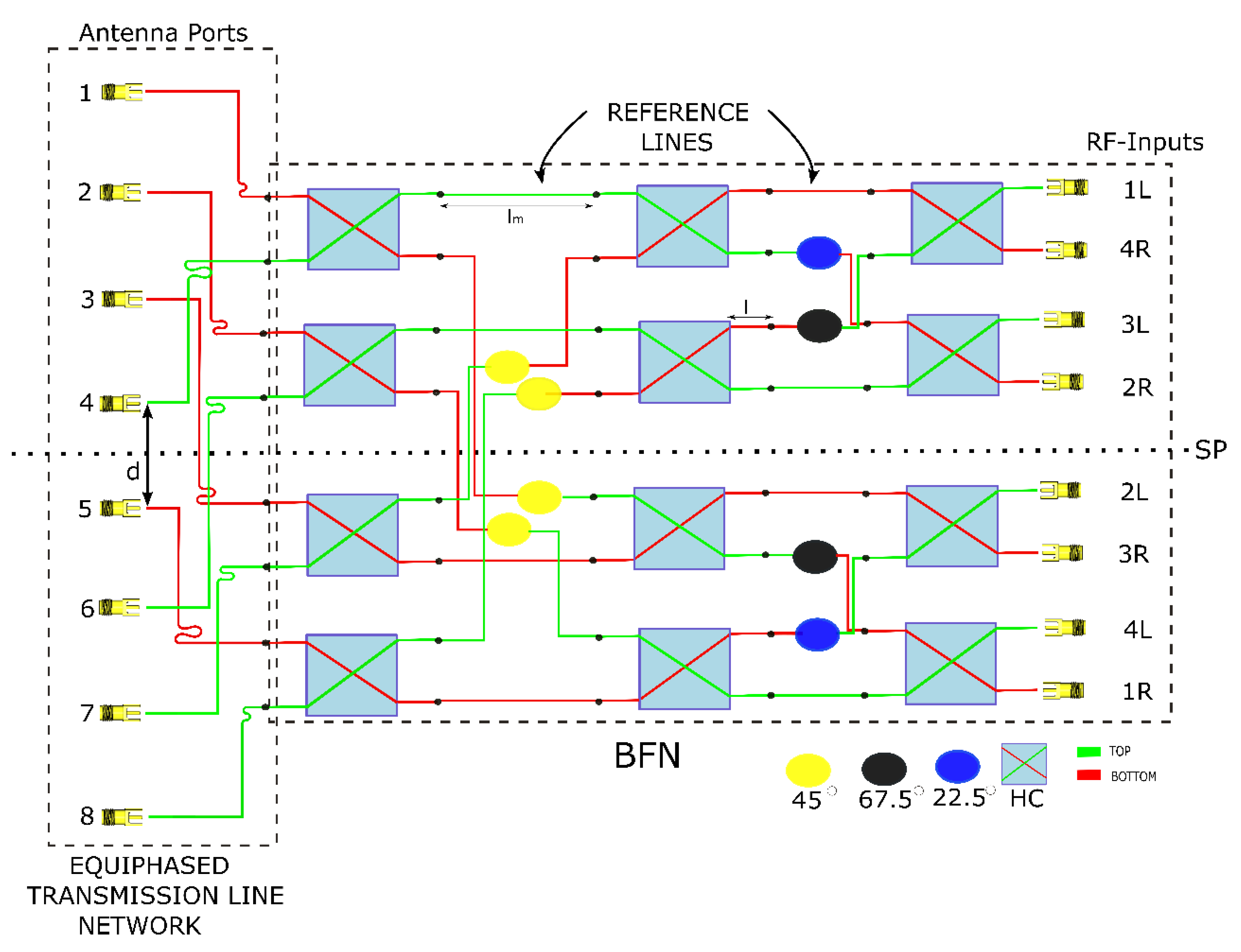
Figure 2 depicts the topology of the proposed BM, which consists of N=2
n=8 (n=3) input ports or excitation ports and N=2
n=8 output ports or antenna ports. Since each input port is electrically connected to the output ports, exciting one of its N inputs produce uniform amplitudes at the outputs with phase difference Δφ. Thus, for every input port excitation there is a different Δφ between the output ports and hence a different beam is produced in the desired direction. Exciting the 8 input ports separately, 8 orthogonal beams are produced at the output, where their radiation field is in the form of sinx/x. The phase difference Δφ at the output ports is calculated as:
where N=8, p=1,2,…..,(n+1) n=7 for 8X8 BM. The beam angular direction θ
p is given as:
where λ is the free space wavelength of the operating frequency and d is the distance of antenna elements at the output ports. Using equation (2) and with respect to
Figure 2 the phase relations between input and output ports and produced beam’s angle are easily derived which are given in
Table 3.
Referring again to the BM topology in
Figure 2, it is comprised of the BFN and the equiphased TL network. The BFN is composed of 12 HCs 3dB/90°, 8 PSs (values shown in
Figure 2) and their corresponding reference lines. The TL network is used to align and order in sequence the BM outputs ports to match to the linear array ports enabling their integration.
The BM design is initially carried out estimating the theoretical dimensions of the HC and PSs following the methodology outlined in our previous works [
30,
31,
32]. Subsequently, we introduce two distinct design approaches for the BM. The first approach involves the design of each component (HC, PSs, TL network) of the 8×8 BM separately and then integrating them to form the overall BM structure. The second approach incorporates the wideband matching technique, as adopted from our preceding work [
33]. With this technique the separate design of each component is avoided since the BM is implemented as a single structure using the theoretical values of the core components and the estimated geometrical characteristic of the interconnecting TLs between them. Moreover, this technique not only facilitates the further miniaturization of the BM by using only the appropriate interconnecting TLs, but also demonstrates adaptability to various passive devices, including six-port networks and beyond.
2.1. Butler Matrix Components Design
2.1.1. 3 dB/90˚ Hybrid Coupler
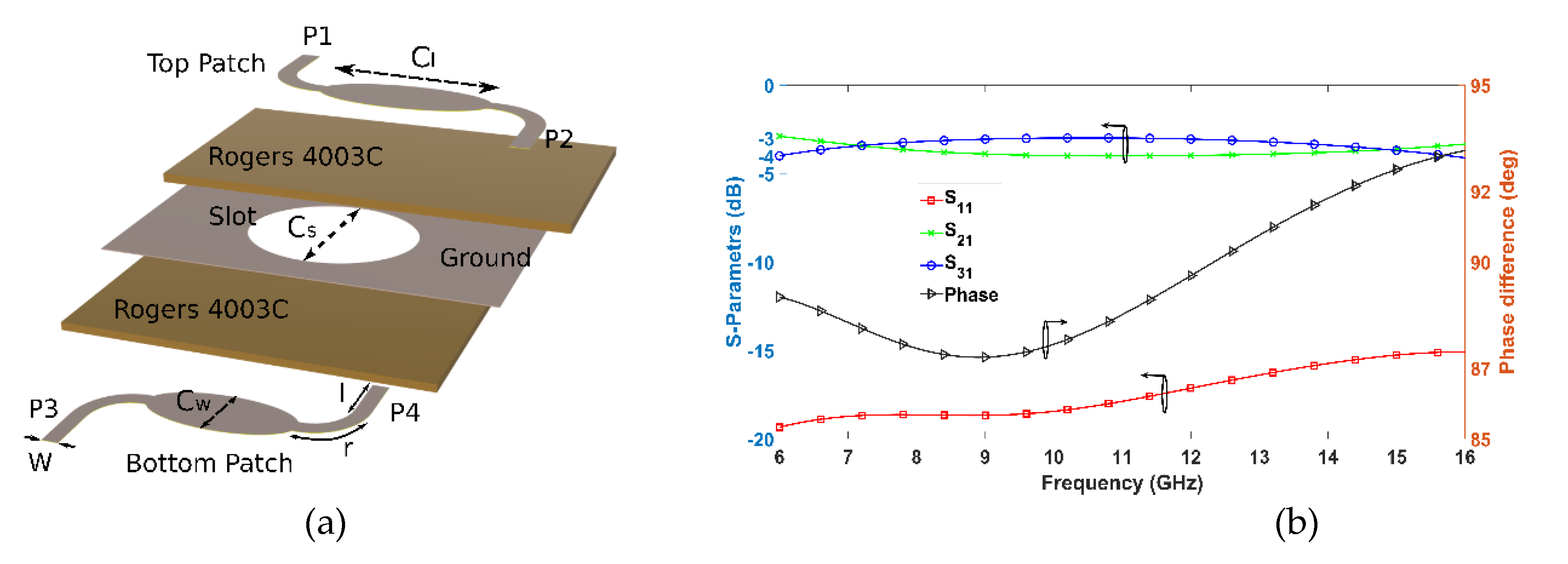
Figure 3a depicts the multilayer structure of the adopted HC, which consists of three conductive layers interleaved with two Rogers 4003C dielectric layers. Elliptically shaped patches are printed on the top and bottom layers, which are coupled through an elliptical slot etched on the middle metallic (ground) layer. Thus, as shown in
Figure 3a, a signal applied to input port P1 is equally divided between output P2 and coupled port P3 with a phase shift of −90°. Ideally there is no signal at the isolated port P4, which is not illustrated in
Figure 3b as it is below -20 dB, with an average value of -20.12 dB.
The coupling C between the P1 input and P3 output as well as the UBW operation of the HC are totally controlled by its geometrical characteristics (
Figure 3a), which are the widths C
w, C
s of the elliptical patch and slot, respectively, and the coupler length C
l. In the design process of the HC, the desired coupling coefficient C=S
31 is initially chosen which defines the outputs power ratio K=P
2/P
3. For an ideal coupler with perfect isolation (S
41=0) and ignoring the presence of small loses, the conservation of power yields (K+1)C
2=1, and therefore it is |S
21|
2=K/(K+1). From the coupling coefficient the even and odd impedances are derived, since the HC of
Figure 3a exhibits a symmetry between ports, thus, supporting the even and odd modes. Subsequently, the parameters C
w, C
s and C
l are calculated using formulas outlined in our previous work, [
30], where a detailed design methodology of the HC and PSs and the calculation of their geometrical characteristics is given. The theoretically estimated and optimized values of the HCs parameters are depicted in
Table 4. The performance of the HC in terms of S-parameters and phase accuracy is illustrated in
Figure 3b. As shown, the transmission parameters S21 and S31 are -3.5 dB for the entire frequency range (6 GHz – 16 GHz) with a negligible deviation of ±0.5 dB, while the reflection coefficient at the input ports is below -15 dB at the same frequency range. Concerning the phase difference between P2 and P3 it is stable at 90° with an acceptable deviation of ±3°.
2.1.2. Phase Shifter and Meander Lines
The same multilayer technology used for the HC is applied to the PSs, with the exception of open-ended ports and the removal of the TLs from ports P2 and P4 of the HC shown in
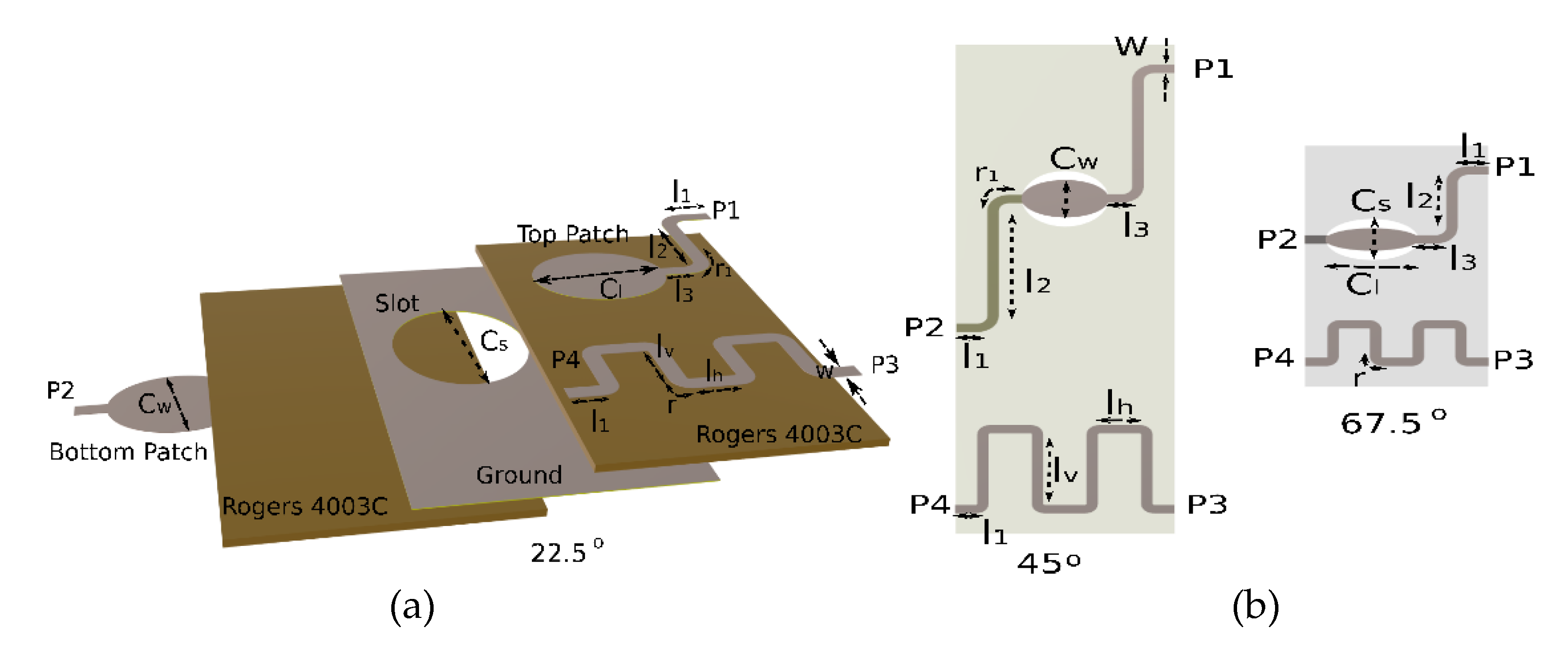
Figure 3a. The obtained two port PS is shown in
Figure 4a. It consists of top and bottom elliptical patches coupled through an elliptical slot located in the middle layer
The phase shift φ
p inserted by the PS is referenced to the phase shift φ
m of a corresponding microstrip line of length l
m=2×l
1+3×l
h+4×l
v+8×(w+r) in order to achieve the desired differential phase Δφ.
The differential phase is influenced by both the coupling coefficient C of the PS and the length of the microstrip line which is also shown in Figure 4a. The coupling coefficient, in turn, is selected based on the required length dictated by the layout. Consequently, the lengths of the patches and slots are set equal to a quarter of the effective wavelength (λ
eff/4), while the widths (Cw and Cs) of the patches and slots, respectively, are determined using again the formulas provided in [
30,
31,
32]. The lengths of the remaining TLs at ports P1 and P2 are adjusted to align with the length of the reference transmission line. In this work, the reference TLs are intentionally meandered to shrink the size of the BM without sacrificing its performance. As outlined in our previous work [
33], when a microstrip line is meandered, it achieves wideband matching characteristics through conjugate matching and admittance compensation, just treating the ML as a shunt component.
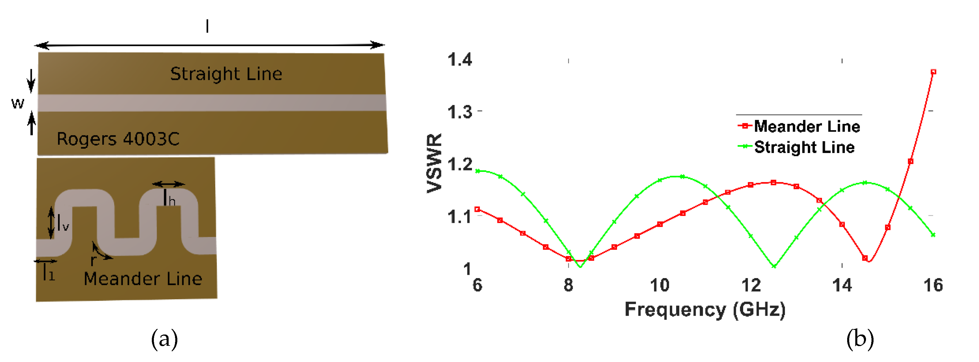
Figure 5a illustrates a TL with a length l alongside its meandered counterpart, which maintains the same length while reducing its footprint to nearly half. In
Figure 5b, the simulated Voltage Standing Wave Ratio (VSWR) of both lines is depicted. Notably, the ML demonstrates equivalent or even superior response within the 6 GHz to 15 GHz range compared to the straight-line configuration, while it remains well below the limit of VSWR=2 over the entire band of 6-16 GHz.
Thus, all the required PSs are designed in conjunction with the MLs while the required coupling and differential phase are achieved tuning the PS elliptic geometry and the vertical length of the MLs. At the same time, the footprint of the PS is effectively reduced resulting further in the compactness of the overall BM as will be shown in section 4. Three PSs were designed and simulated herein. A 22.5° PS shown in exploded view (
Figure 4a) followed by a 45° and a 67.5° PS shown in a layout view (
Figure 4b) both sharing the same layer stack as the 22.5° PS. All parameters depicted in
Figure 4 and their corresponding values for the three PSs are listed in
Table 4, while
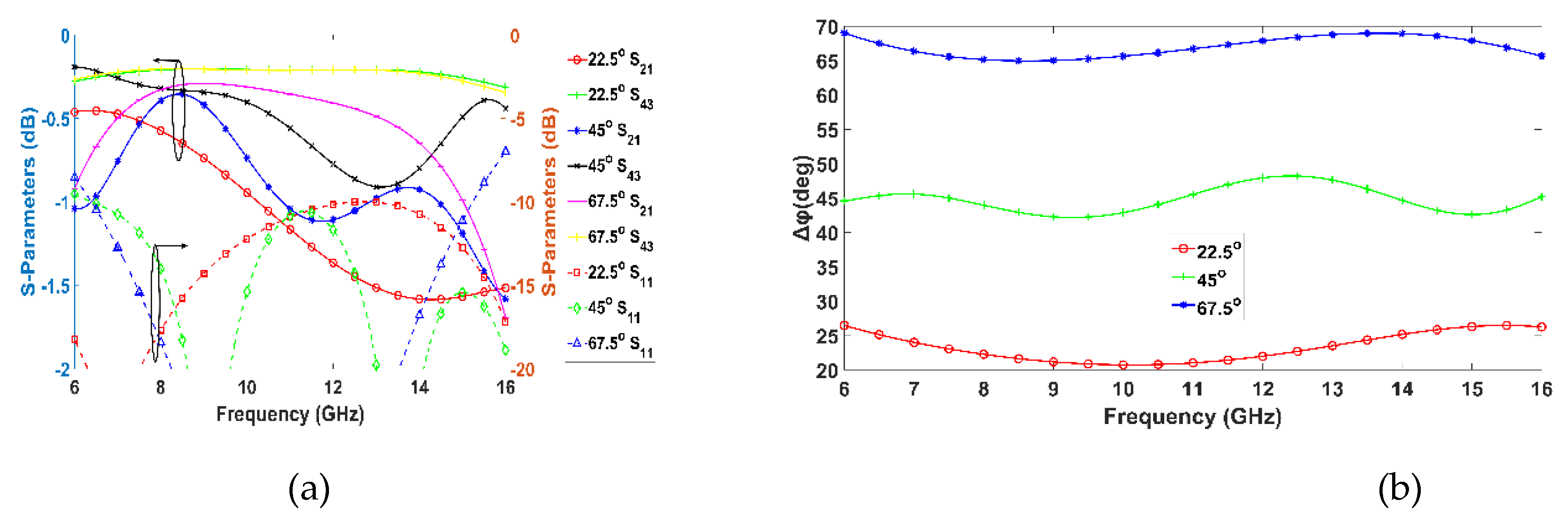
Figure 6 illustrates the performance of the PSs in terms of S-parameters accuracy and differential phase, between the PS path and the corresponding microstrip line or ML. As shown in
Figure 6a the transmission coefficient (S
21) for the PSs as expected exhibits an insertion loss of -1 dB or less, with a maximum deviation of 0.6 dB at 16 GHz, while the reflection coefficient (S
11) is below -10 dB for almost the whole frequency range. The maximum deviation for the transmission coefficient (S
43) of MLs is 0.5 dB at 13 GHz from the expected value of -0.3 dB. Excellent agreement between the ideal - theoretical and the simulated differential phase is achieved for the three PSs as shown in
Figure 6b, where a maximum deviation of 3° for the 22.5° PS is observed.
Table 5.
Final values of the parameters of the three PSs. T denotes theoretical and S denotes simulated.
Table 5.
Final values of the parameters of the three PSs. T denotes theoretical and S denotes simulated.
| |
Cw
|
Cs
|
Cl
|
W |
l1
|
l2
|
l3
|
lh
|
lv
|
r |
r1
|
| |
T |
S |
T |
S |
T |
S |
| 22.5° |
4.21 |
3.72 |
5.21 |
5.32 |
5.01 |
4.5 |
0.54 |
1 |
3 |
0.807 |
1.372 |
1.705 |
0.06 |
0.5 |
| 45° |
3.4 |
2.7 |
3.9 |
3.7 |
4.7 |
4.2 |
0.54 |
1 |
7.024 |
0.643 |
1.953 |
4.63 |
0.06 |
0.5 |
| 67.5° |
2.5 |
1.47 |
2.75 |
2.76 |
4.59 |
4.5 |
0.54 |
1 |
3 |
0.807 |
1.372 |
1.801 |
0.06 |
0.5 |
2.1.3. Equiphased Transmission Line Network
Figure 7a illustrates the equiphased TLs network which is employed to rearrange the outputs ports of the BM to achieve the desired phase shift Δφ (
Table 3) between them and to facilitate the integration of the linear Vivaldi antenna array. Only the four out of the eight lines are depicted in
Figure 7a, since our BM exhibit symmetry as shown in
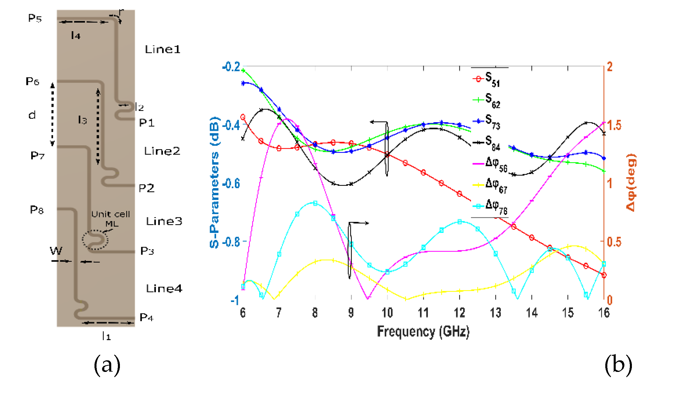
Figure 2. Those lines are structured in a reversed ‘S’ shape configuration and positioned at distance d, where d=0.6×λ
min=0.6×c/f
max. This distance allows for a direct connection to the corresponding antenna ports. It is selected to ensure the avoidance of grating lobes in the radiation pattern even for the two far end steered beams expected at angles θ
max=±45
° from broadside. According to Balanis [
34] this restriction reads:
Additionally, each of the four lines integrate a unit cell ML which serves to equalize their physical lengths, thereby compensating - zeroing the phase difference between them.
The parameters for the four TLs shown in
Figure 7a and their values are listed in
Table 6, while
Figure 7b depicts the transmission S-parameters and phase difference of the TLs. A maximum loss is observed for the first line where the S
51 transmission parameter is -0.9 dB at 16 GHz. Maximum phase deviation of 1.5° from zero is observed between lines 5 and 6.
2.2. BM Design Employing Wideband Matching Technique
The second approach elaborating on the design of BM as a single unified structure is now presented.
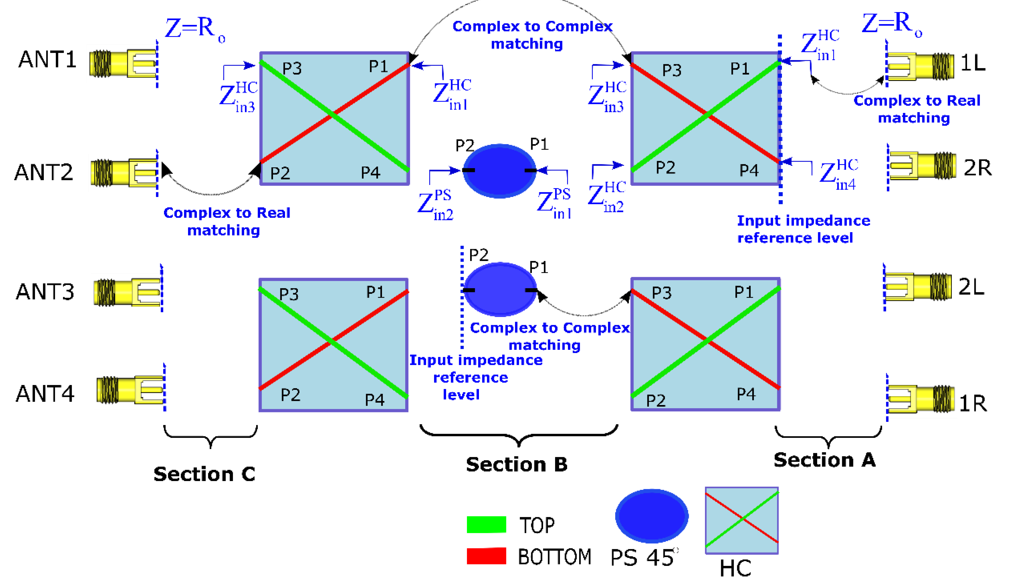
Figure 8 illustrates the concept of the wideband matching technique utilized to design a BM in the 6 – 16 GHz band. For illustrative purposes, the design of a 4×4 BM is presented here, however, the method is identical for the design of an 8×8 BM. The 4×4 BM is the classical BM consisting of four HCs and two 45° PSs. As shown in
Figure 8 the TLs connecting the HCs ports to the input and output ports are removed (Sections A and C). Additionally, the interconnecting TLs and those connecting the PSs ports to the HCs ports (Section B), are also eliminated leaving only the HCs and PSs as the core components. The theoretical parameters related to the geometry of the core components are given in
Table 4 (Section 3.1) for the HC and in
Table 5 (
Section 3.2) for the PS. Thus, the input impedance at the reference plane, depicted in
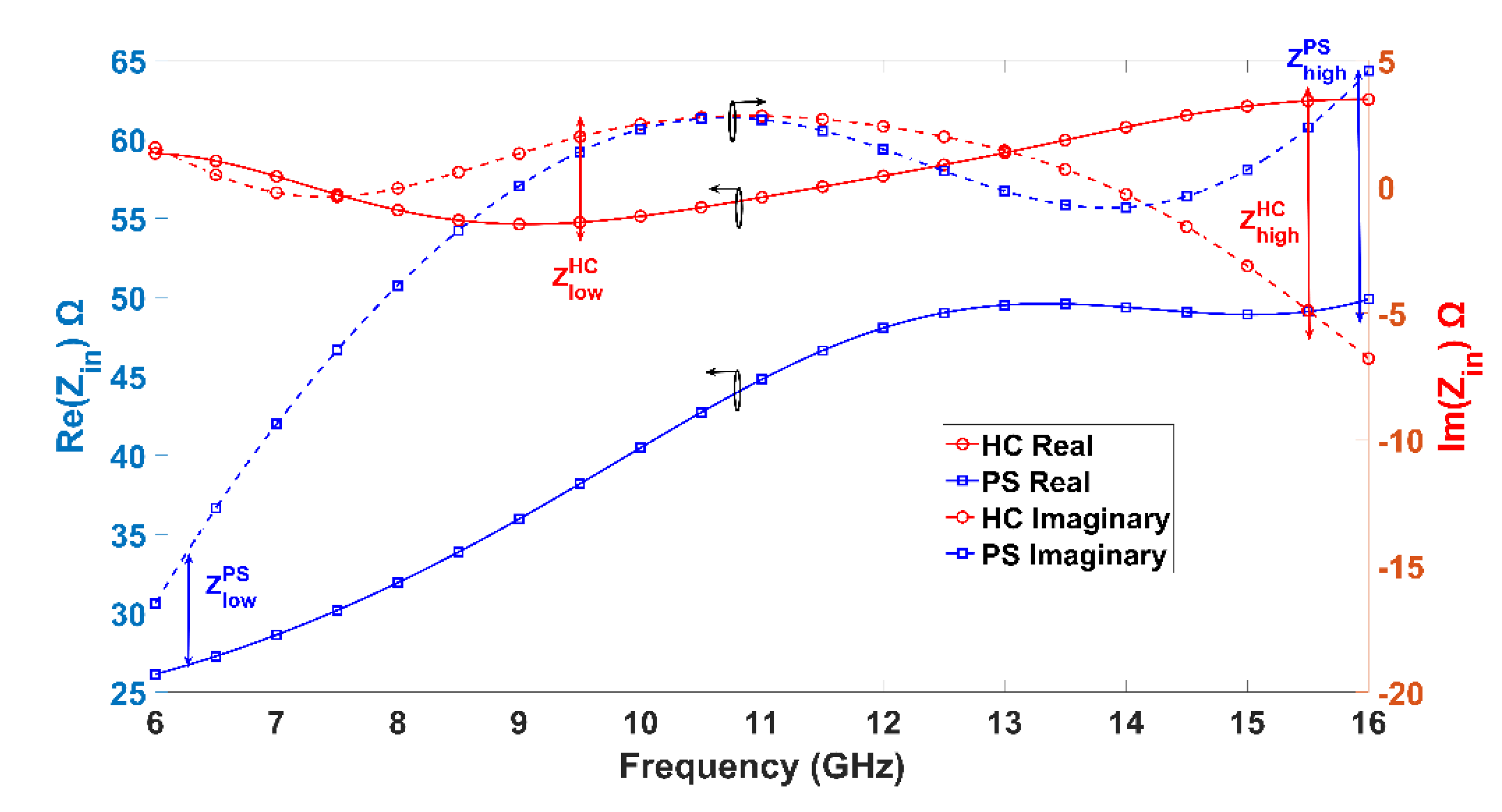
Figure 8, is initially estimated through simulation for each core component. The simulated input impedance for the HC and for the PS is depicted in
Figure 9 where the real and the imaginary parts are plotted. Form the input impedances, the low - min and high - max impedances for each component are easily obtained from the plots as Z
low=R
low+jX
low and Z
high=R
high+jX
high. Subsequently, the hyperbolic mean impedance Z
m=R
m+jX
m is computed for the HC and PS from the relation given in our previous work, [
33]. Due to the symmetry and reciprocity inherent in the core components it is evident that the hyperbolic mean impedance will be identical for all ports of both the HC and PS. Therefore, we have Z
HCm1= Z
HCm2= Z
HCm3= Z
HCm4 and Z
PSm1= Z
PSm2. The next step is to determine the appropriate characteristic impedance Z
o of the interconnecting TLs between the core components and between the input and output ports using equation (5) taken from [
33] and repeated herein in order to clarify the procedure.
In equation (5) Z
A and Z
B represent the hyperbolic mean impedances of the components to be matched. Thus, to compute for example, the characteristic impedance of the TL connecting the HC’s port P1 to connector port 1L (
Figure 8), a complex to real matching is applied, since it is connected to 50 Ω connector and hence, in equation (5), Z
A=50 Ω and Z
B= Z
HCm1. A complex to real matching is applied also for the estimation of TLs connecting the HC ports to the output connector ports (ANT1 – ANT4). A complex-to-complex matching is applied for the interstage components. Specifically, to match for example, PS port P1 to HC port P2 (
Figure 8) it should be Z
A= Z
HCm2 and Z
B= Z
PSm1, while to estimate the matching reference line connecting the HC’s port P3 to the next HC’s port P1 it should be Z
A= Z
HCm3 and Z
B= Z
HCm1. Except the characteristic impedance of the TLs, the electrical length of them is also estimated using equation (17) given in [
33]. However, for the BM in
Figure 8 only the length of the TLs connecting the HCs ports to the input connectors (1L, 2R, 2L and 1R) is determined. This is because the lengths of the interstage TLs, as well as those at the output ports, are dictated by the required differential phase and the geometry of the equiphased TL network, respectively. Therefore, their estimation is omitted herein. The last step is to compute the appropriate width (W) and length (L) of the interconnecting TLs using well known equations found in [
35].
Table 7 depicts the Z
low, Z
high and the estimated Z
m of the HC and PS ports as well as the geometrical characteristics of their corresponding interconnecting TLs.
Thus, using the theoretical values for the core components and the estimated geometrical characteristics (width and length) of the interconnecting TLs, a 4×4 BM is designed as will be shown in section 3.2. The same design approach is employed to design an 8×8 BM operating again in the 6 – 16 GHz band.
3. Butler Matrix Results
3.1. 8×8. BM Results of the 1st Design Approach
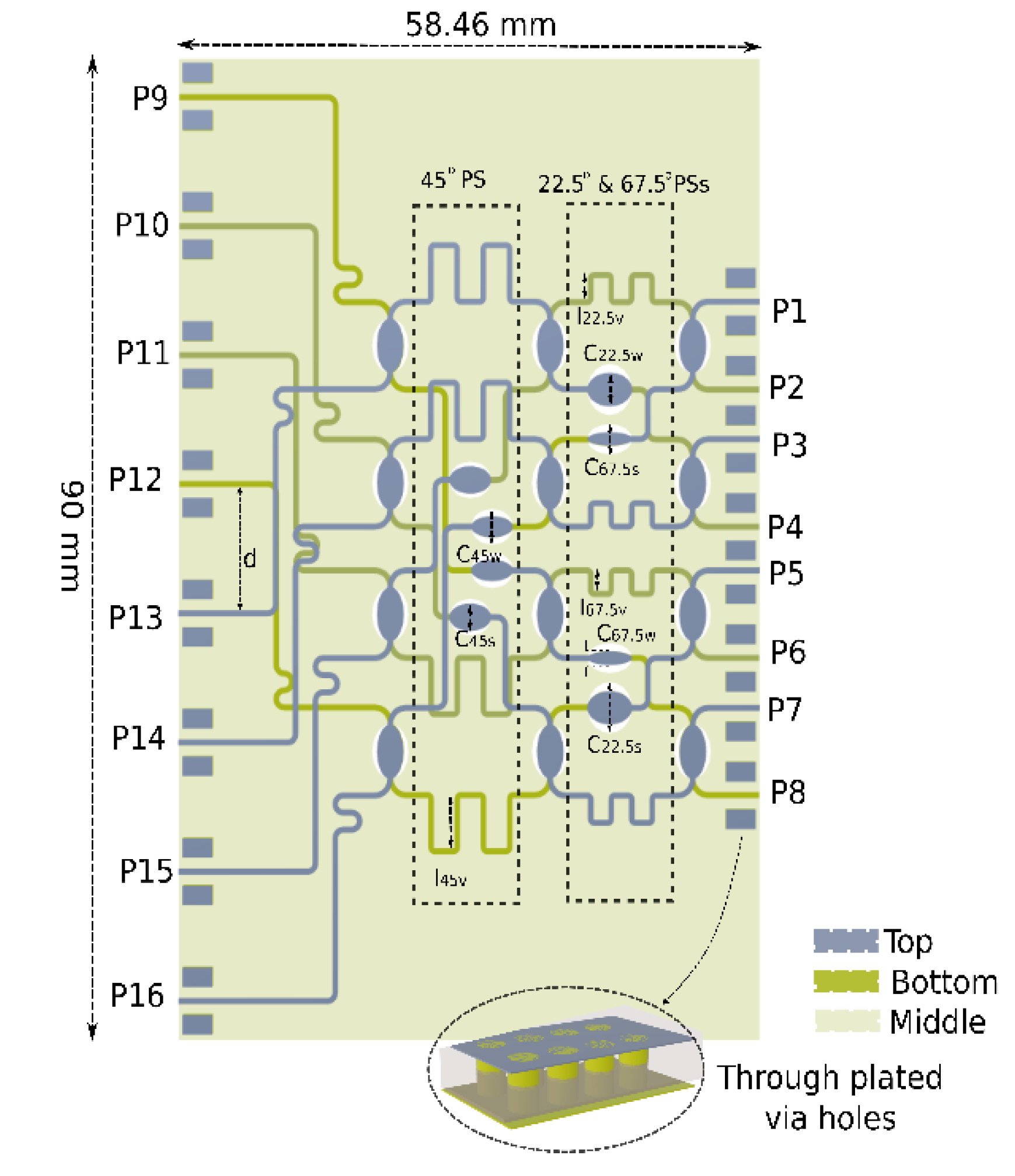
Figure 8 shows a schematic view of our proposed BM. The multilayer structure is comprised of three conductive layers interleaved with two dielectric layers. Notably, the dielectric layers are not shown here to provide a clear view of the top and bottom patches as well as the ground layer. It is worth mentioning that each key component was individually designed as demonstrated in section 2.1 with a 50 Ω characteristic impedance for both input and output lines - connectors. Consequently, when these components are assembled to create the overall structure, there is a degree of mismatch at the connection points due to slight deviations from the exact 50 Ω characteristic impedance at the input and output connectors of each component. This mismatch results in a slight variation in transmission coefficient for each path altering the phase as well. Hence, the parameters denoted in
Figure 8 which are related to PSs and MLs geometry are further tuned to get their final optimized values listed in
Table 8. Specifically, the vertical lengths l
22.5v, l
45v and l
67.5v are tuned to keep the differential phase between output ports around the target value, while the widths C
w and C
s for each PS are tuned to reduce the ripples of each Δφ. As shown in
Table 8, the maximum percentage change occurs for the vertical length l
67.5v which is 17%. For adequate grounding and to minimize parasitic effects, additional 4 mm long lines with 0.4 mm diameter through-plated via holes have been placed at each port, as shown in
Figure 8. These modifications facilitate measurements using SMA or SMP connectors. The total achieved size of the BM is 58.46 mm × 90 mm or 5.6
FA. Notably, since the length of the vertical side of the BM is defined by the length of the TLs network, miniaturization achieved (through the integration of the MLs) on the horizontal side of the BM effectively reducing its FA.
Figure 8.
Designed 8×8 BM.
Figure 8.
Designed 8×8 BM.
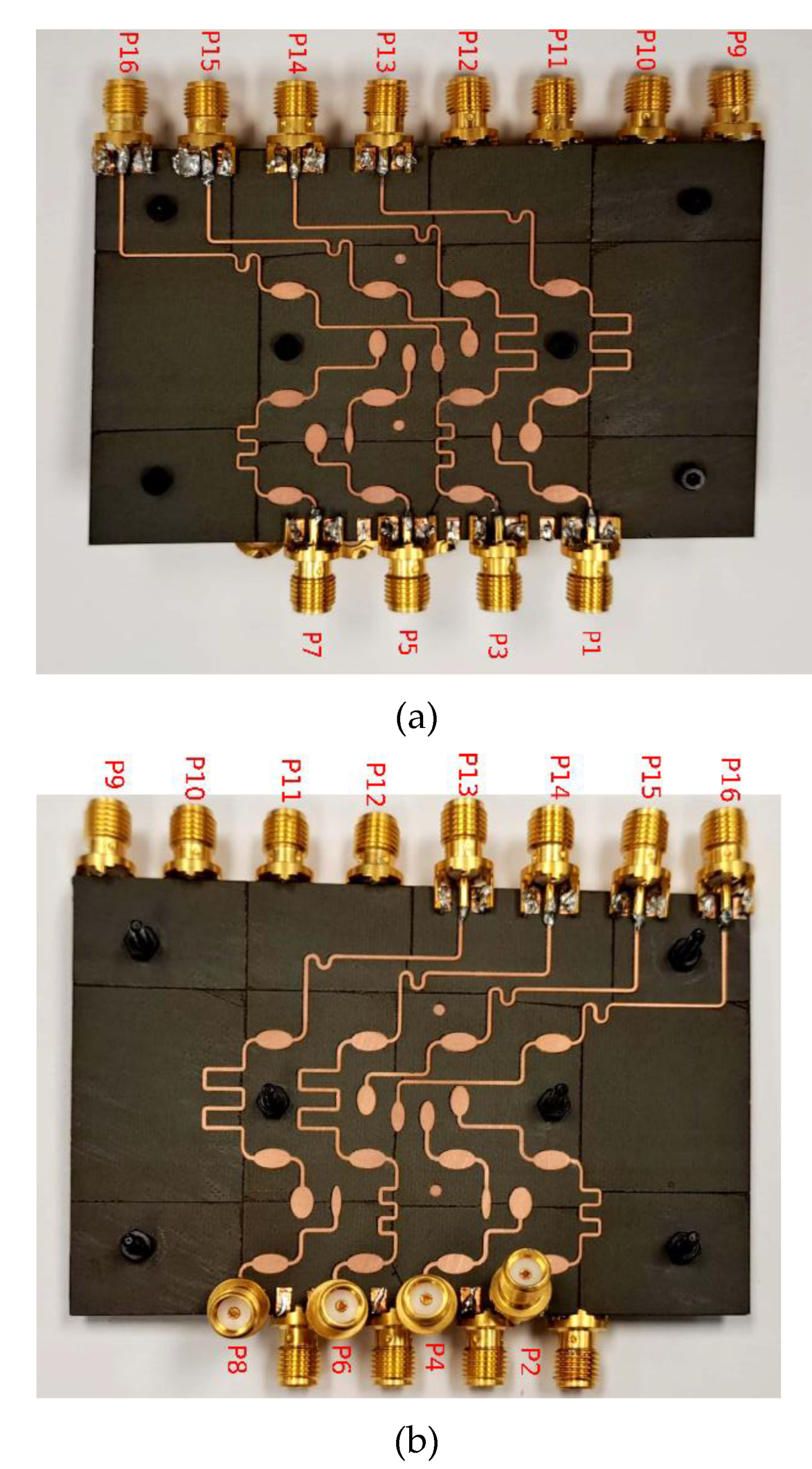
Figure 9.
Fabricated 8×8 BM prototype. (a) Top view and (b) bottom view.
Figure 9.
Fabricated 8×8 BM prototype. (a) Top view and (b) bottom view.
The fabricated BM prototype is depicted in
Figure 9, printed into separated boards which are aligned appropriately and bonded together in a back-to-back configuration. Due to the limited amount of space at the input side of the BM, the SMA connectors that corresponds to the input ports (right side of
Figure 9b) of the bottom layer were attached vertically. Rogers 4350B with ε
r=3.34 and thickness h of 0.25 mm was utilized for the two dielectric layers.
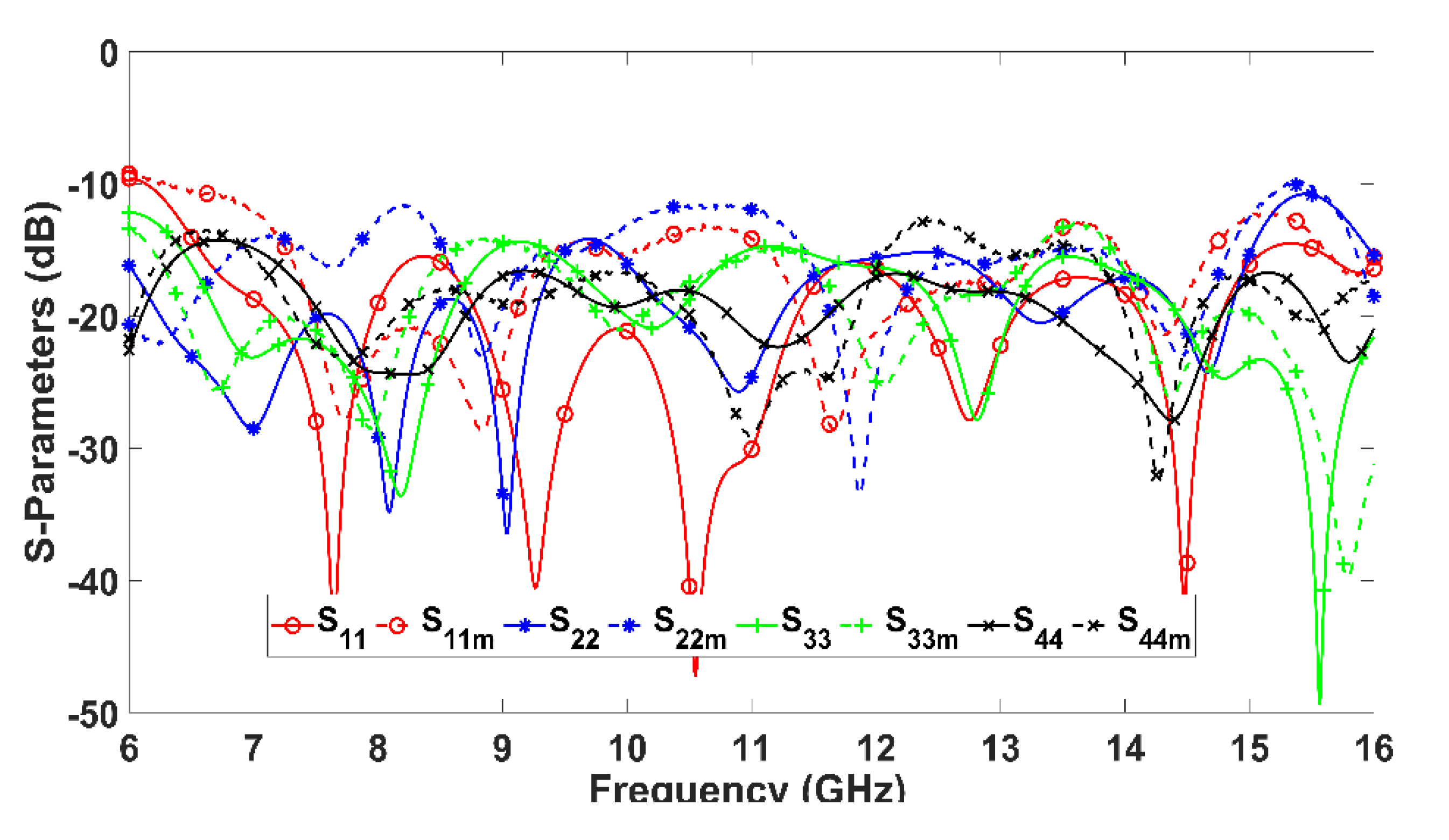
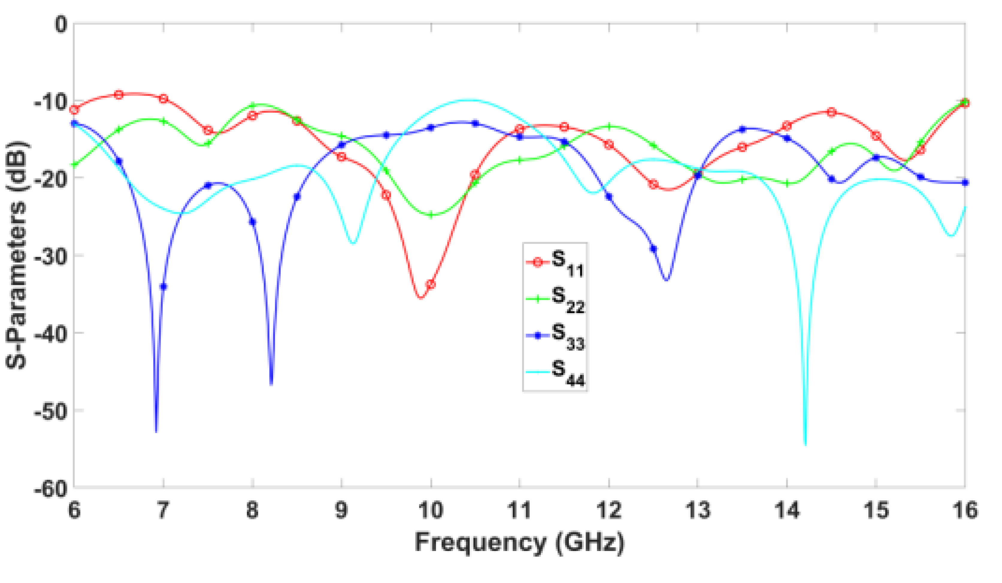
Figure 10 illustrates the simulated and measured reflection coefficient of the input ports for the 8×8 BM of
Figure 8 and
Figure 9. Given the symmetry of the BM’s topology shown in
Figure 2, the response from four out of eight ports suffices for illustration purposes. Consequently, the responses of the remaining ports is identical. Hence, S
11=S
88, S
22=S
77, S
33=S
66 and S
44=S
55. As shown in
Figure 10, both the simulated and measured reflection coefficient remains below -10 dB for the entire frequency range from 6 to 16 GHz.
Figure 11,
Figure 12,
Figure 13 and
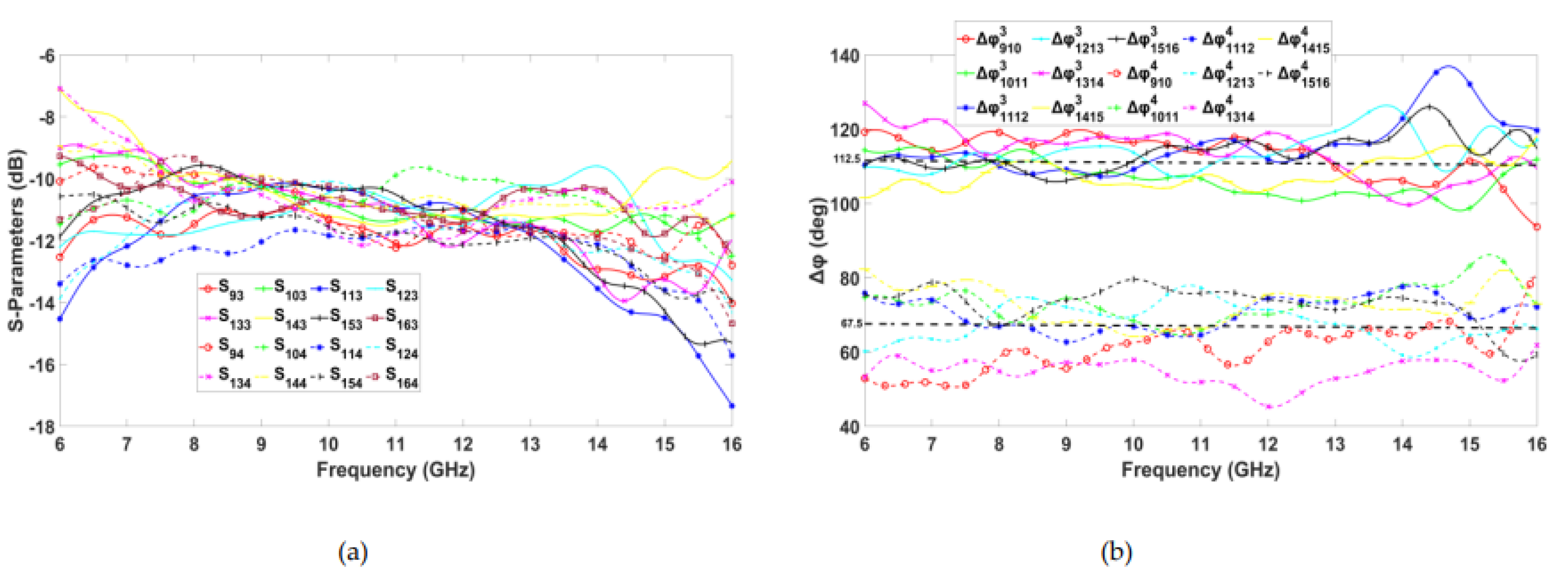
Figure 14 illustrate the simulated and measured transmission responses and phase differences obtained at the output ports when input ports 1, 2, 3, and 4 are excited. Due to the symmetrical design, the responses for ports 5, 6, 7, and 8 are identical. The expected transmission coefficients to the output ports are around -12 dB. This is because a signal applied to the input ports will traverse three HCs and two PSs, or a PS with an ML, or two MLs to reach the output ports. Notably, an ideal 8×8 BM divides the input power equally to its 8 output ports, thus, an S
21 of -9 dB would result. Hence, the measured -12 dB observed includes 3 dB losses across the entire path. Observing
Figure 11a to
Figure 14a, there is a good agreement between simulated and measured transmission coefficients from input to output ports when input ports 1 to 4 are excited, respectively. Their magnitude is around -12 dB with a ±3 dB deviation across the frequency range from 6 to 15 GHz. Considering the 6 GHz – 15 GHz range as the band of operation, the achieved FBW of the proposed BM is 92% which is the highest as compared against related works in
Table 2.
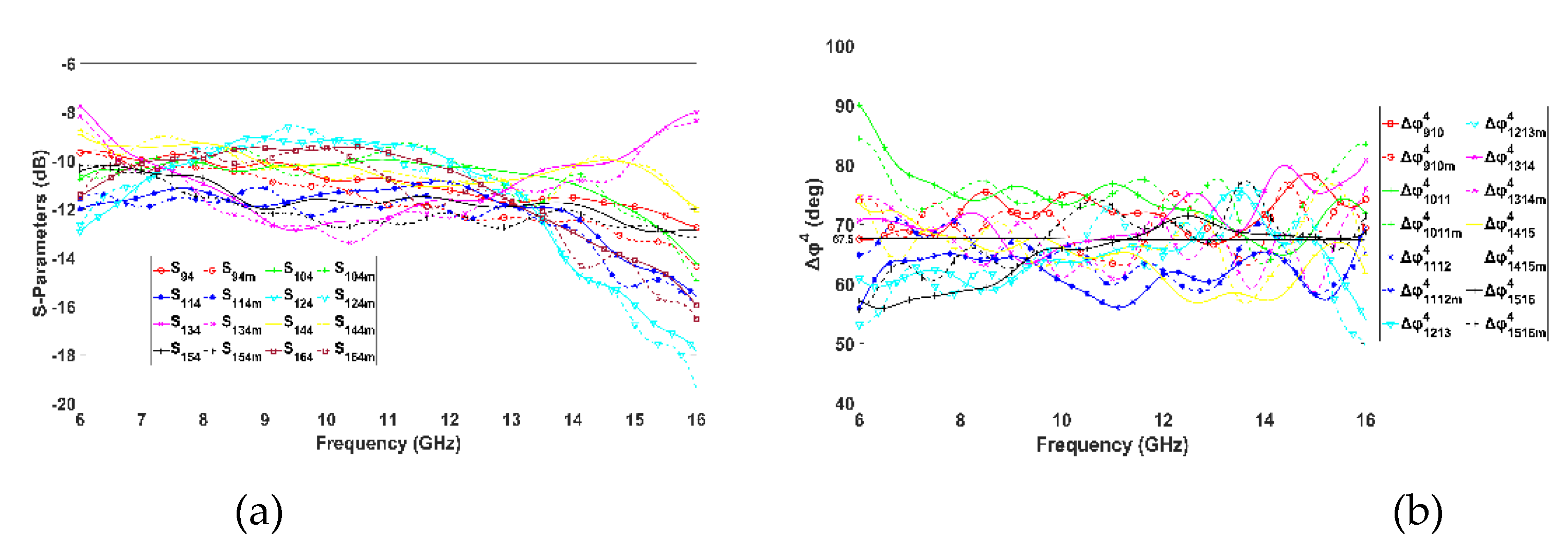
Regarding the phase difference at output ports for each input ports excitation, as depicted from
Figure 11b to
Figure 14b, the maximum deviation Δφ from the ideal values occurs for the measured phase differences. Specifically, for port 1 its phase deviation is Δφ
1=15°, for port 2 Δφ
2=16°, for port 3 Δφ
3=20° and for port 4 Δφ
4=21.5°. The phase variations of the proposed BM are relatively high, which was anticipated given the UWB operation. Phase accuracy tends to vary linearly with BW, hence, the wider the BW, the more significant the phase variations.
Moreover, despite the phase variations, the generated beam pattern of the BM experiences minimal impact, as illustrated in
Figure 15. This figure illustrates the gain of each beam when the output ports of the BM feed into a uniform linear array. For this purpose, the simulated and measured S-parameters were imported in an antenna array simulation tool representing the excitation amplitude and phase. As shown in
Figure 15, a very good agreement is obtained between the theoretical (
Table 3), the simulated and the measured beam angles.
3.2. BM Results of the 2nd Design Approach
Using the estimated geometrical characteristics of the interconnecting TLs from
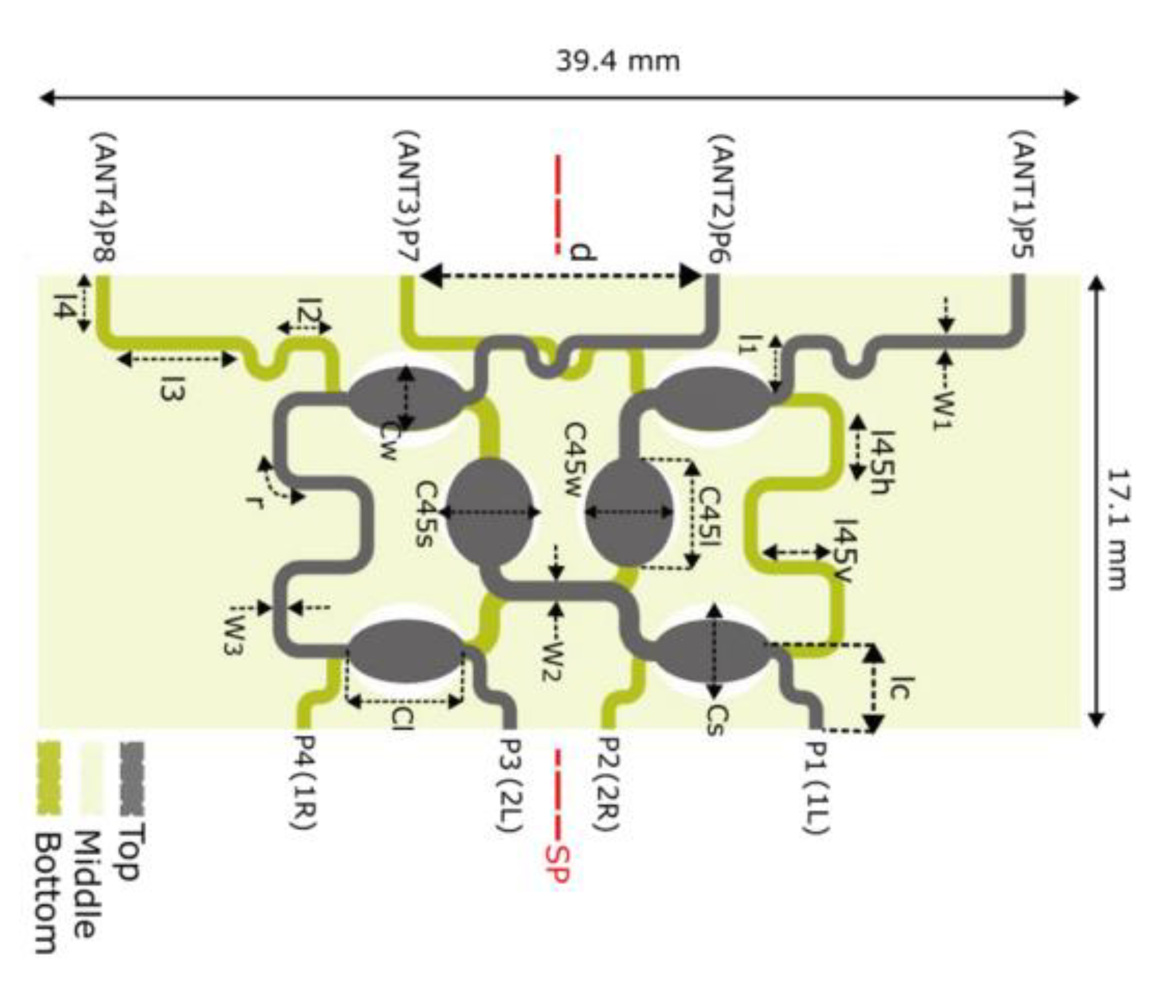
Table 7, a 4×4 BM was implemented as shown in
Figure 16. Each section (input, output and interstage) is designed given the widths tabulated in
Table 7. Additionally, the reference TLs connecting the HCs are meandered once again resulting in a BM size of 39.4 mm × 17.1 mm or 0.74
. The theoretical parameters of the HC and 45° PS (shown in the parenthesis of
Table 9) are optimized with their final values provided in
Table 9.
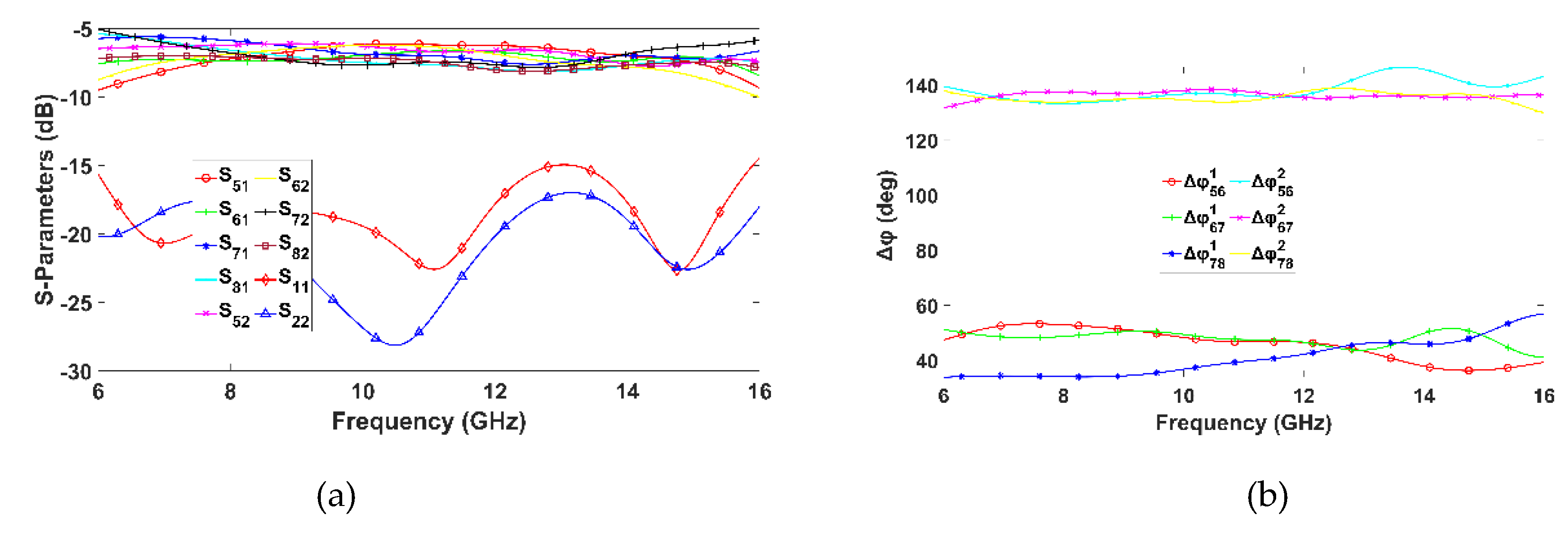
Figure 17 depicts the performance of the 4×4 BM in terms of S-parameters and phase accuracy. Since the network is symmetric, result for ports 1 and 2 only are illustrated. As shown in
Figure 17a the insertion loss of the BM exciting ports P1 and P2 is as expected around -7 dB with a ±2 dB deviation in the entire 6 GHz -16 GHz band. The reflection coefficient of the BM is below -10 dB for the entire band of operation. Regarding the phase difference at the output ports, Δφ=45° is expected between them when port P1 is excited, while Δφ=135° is expected when port P2 is excited. Indeed, as shown in
Figure 17b the obtained phase difference is around 45° and 135° exciting P1 and P2, respectively, with maximum deviation of 9° for P1 excitation. Considering the S-parameter and phase response of the 4×4 BM the achieved FBW is 102% which is the highest compared to the works reported in
Table 1. Additionally, the design maintains a compact size, comparable to or even smaller than those reported in
Table 1.
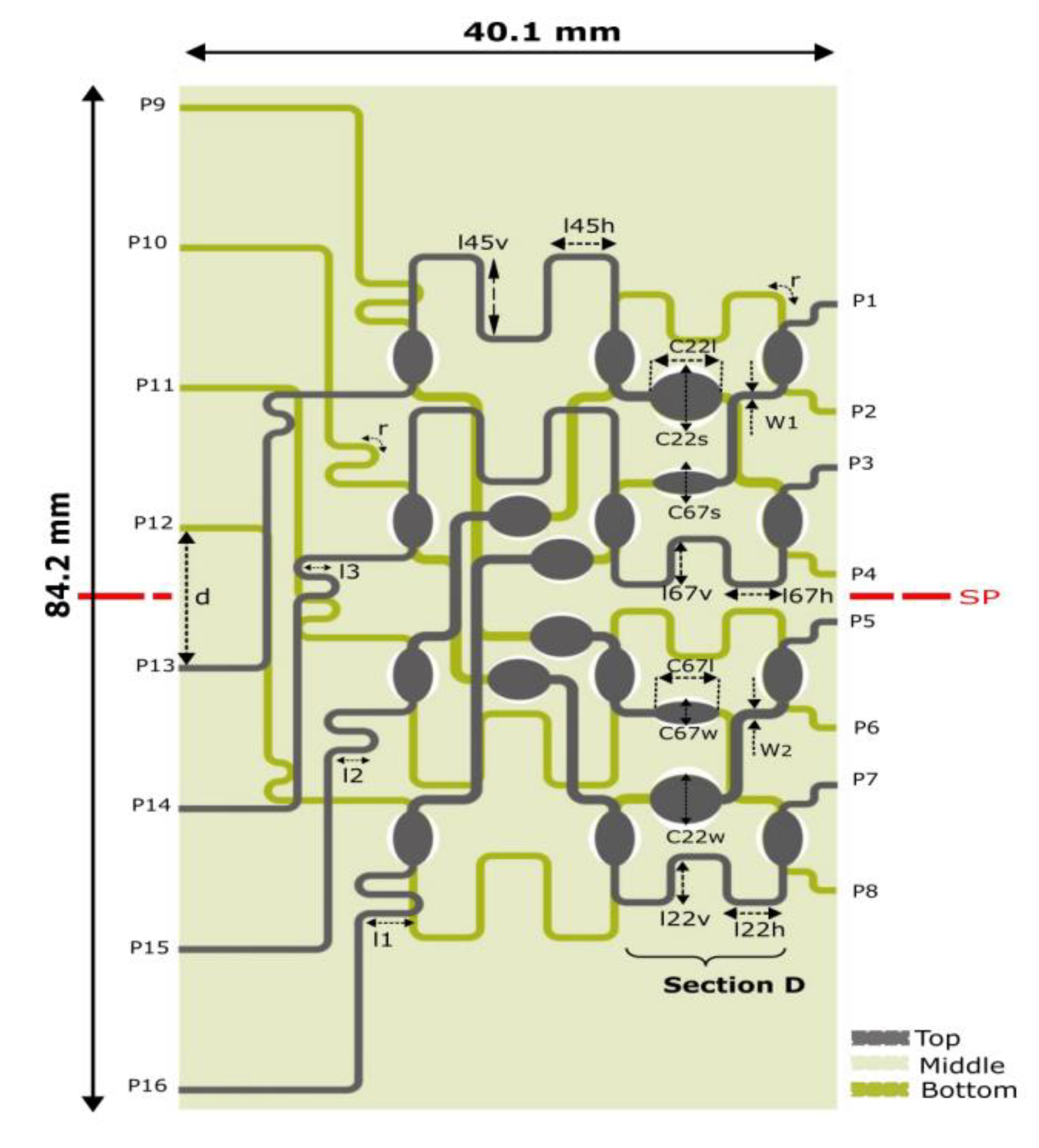
Following the same procedure used for the 4×4 BM, an 8×8 BM was designed utilizing the wideband matching technique described in
Section 2.2. Herein, in the estimation of the geometrical characteristics of interconnecting TLs an extra section (Section D) is added as shown in
Figure 18 which contains the 22.5° and 67.5° PSs and their related reference TLs. The estimated widths are given in the caption of
Figure 18. The theoretical parameters (shown in the parenthesis of
Table 10) of the 22.5° and 67.5° PSs are optimized with their final dimensions provided in
Table 10. Since BM is designed as a single – unified structure using only the appropriate TLs to interconnect the core components, the total achieved size is 84.2 mm × 40.1 mm or 3.57
. This design represents an approximate 20% miniaturization compared to the previous 8×8 BM design outlined in
Section 2.1.
Figure 19 depicts the simulated reflection coefficient at the input ports of the 8×8 BM presented in
Figure 18. As shown, the reflection coefficient is maintained below -10 dB across the entire operational bandwidth.
Figure 20 and
Figure 21 illustrate the simulated transmission responses and phase differences obtained at the output ports when input ports 1, 2, 3, and 4 are excited. Due to the symmetrical design, the responses for ports 5, 6, 7, and 8 are identical. The simulated transmission coefficients from input to output ports for each port excitation are approximately -12 dB with a deviation of a ±3 dB within the frequency range of 6 to 15 GHz, as demonstrated in
Figure 20a and
Figure 21a. Considering its ideal value of -9 dB resulting from the 1 to 8 power division, the additional -3 dB corresponds to power losses. Concerning the phase difference Δφ at output ports for each input ports excitation, as illustrated in
Figure 20b and
Figure 21b, a maximum deviation of 21° from the ideal values occurs between output ports P11-P12 when port P3 is excited. The same FBW is achieved as the BM designed in
Section 2.1. Notably, a reduction in footprint area (FA) by 36% is attained in this design, resulting in the best compromise between FBW and size compared to the reported works in
Table 2
Figure 1.
Multibeam antenna array exploiting 3D Beamformer based on Butler matrix feeding Tapered Slot Antenna Array.
Figure 1.
Multibeam antenna array exploiting 3D Beamformer based on Butler matrix feeding Tapered Slot Antenna Array.
Figure 2.
8×8 Butler Matrix Topology. SP denotes symmetry plane.
Figure 2.
8×8 Butler Matrix Topology. SP denotes symmetry plane.
Figure 3.
(a) Hybrid Coupler layers stack up. W=0.54, l=1.66 and r=1.26 (Dimensions are in mm). (b) Simulated S-Parameters and phase difference between ports 2 and 3, for an RF-input at port-1.
Figure 3.
(a) Hybrid Coupler layers stack up. W=0.54, l=1.66 and r=1.26 (Dimensions are in mm). (b) Simulated S-Parameters and phase difference between ports 2 and 3, for an RF-input at port-1.
Figure 4.
(a) Layers stack of 22.5° PS. (b) Layout of 45° and 67.5° PSs.
Figure 4.
(a) Layers stack of 22.5° PS. (b) Layout of 45° and 67.5° PSs.
Figure 5.
(a) Straight line and its equivalent ML, l=20, w=1, l1=0.5, lv=1.7, lh=1.3 and r=0.01, (Dimensions are in mm). (b) VSWR plot of the two lines.
Figure 5.
(a) Straight line and its equivalent ML, l=20, w=1, l1=0.5, lv=1.7, lh=1.3 and r=0.01, (Dimensions are in mm). (b) VSWR plot of the two lines.
Figure 6.
(a) S-parameters and (b) differential phase for the three PSs.
Figure 6.
(a) S-parameters and (b) differential phase for the three PSs.
Figure 7.
(a) Layout of the equiphased TLs network. (b) Transmission S-parameters and differential phase between the lines.
Figure 7.
(a) Layout of the equiphased TLs network. (b) Transmission S-parameters and differential phase between the lines.
Figure 8.
Wideband matching technique utilized to design a 4×4 BM. All interconnecting TLs are initially removed to be replaced by appropriate MLs.
Figure 8.
Wideband matching technique utilized to design a 4×4 BM. All interconnecting TLs are initially removed to be replaced by appropriate MLs.
Figure 9.
Real and imaginary parts of the input impedances of the HC and PS at input reference level.
Figure 9.
Real and imaginary parts of the input impedances of the HC and PS at input reference level.
Figure 10.
Reflection coefficient of input ports of our proposed 8×8 BM. m denotes measurements.
Figure 10.
Reflection coefficient of input ports of our proposed 8×8 BM. m denotes measurements.
Figure 11.
Port 1 excitation. (a) Transmission coefficients Si1 from input port 1 to output ports, i=9,..,16. (b) Phase difference of output ports (ideal 22.5˚). Superscript 1 denotes the input port and subscript ij denotes the consecutive output ports, m denotes measurements.
Figure 11.
Port 1 excitation. (a) Transmission coefficients Si1 from input port 1 to output ports, i=9,..,16. (b) Phase difference of output ports (ideal 22.5˚). Superscript 1 denotes the input port and subscript ij denotes the consecutive output ports, m denotes measurements.
Figure 12.
Port 2 excitation. (a) Transmission coefficients Si2 from input port 2 to output ports, i=9,..,16. (b) Phase difference of output ports (ideal 157.5˚), superscript 2 denotes the input port and subscript ij denotes the consecutive output ports, m denotes measurements.
Figure 12.
Port 2 excitation. (a) Transmission coefficients Si2 from input port 2 to output ports, i=9,..,16. (b) Phase difference of output ports (ideal 157.5˚), superscript 2 denotes the input port and subscript ij denotes the consecutive output ports, m denotes measurements.
Figure 13.
Port 3 excitation. (a) Transmission coefficients Si3 from input port 3 to output ports, i=9,..,16. (b) Phase difference of output ports (ideal 122.5˚). Superscript 3 denotes the input port and subscript ij denotes the consecutive output ports, m denotes measurements.
Figure 13.
Port 3 excitation. (a) Transmission coefficients Si3 from input port 3 to output ports, i=9,..,16. (b) Phase difference of output ports (ideal 122.5˚). Superscript 3 denotes the input port and subscript ij denotes the consecutive output ports, m denotes measurements.
Figure 14.
Port 4 excitation. (a) Transmission coefficients Si4 from input port 4 to output ports, i=9,..,16. (b) Phase difference of output ports (ideal 67.5˚). Superscript 4 denotes the input port and subscript ij denotes the consecutive output ports, m denotes measurements.
Figure 14.
Port 4 excitation. (a) Transmission coefficients Si4 from input port 4 to output ports, i=9,..,16. (b) Phase difference of output ports (ideal 67.5˚). Superscript 4 denotes the input port and subscript ij denotes the consecutive output ports, m denotes measurements.
Figure 15.
Simulated and measured radiation pattern of the 8×8 BM, d=0.6λmin. The corresponding theoretical beam directions are ±46˚, ±31˚, ±18˚ and ±6˚ respectively.
Figure 15.
Simulated and measured radiation pattern of the 8×8 BM, d=0.6λmin. The corresponding theoretical beam directions are ±46˚, ±31˚, ±18˚ and ±6˚ respectively.
Figure 16.
Implemented 4×4 BM. W1=0.49, W2=0.68, W3=0.41, lc=5.48, l45v=1.74, l45h=1.63, l1=1, l2=0.8, l3=4.5, l4=2 and r=0.5. All dimensions are in mm.
Figure 16.
Implemented 4×4 BM. W1=0.49, W2=0.68, W3=0.41, lc=5.48, l45v=1.74, l45h=1.63, l1=1, l2=0.8, l3=4.5, l4=2 and r=0.5. All dimensions are in mm.
Figure 17.
(a) S-parameters of the 4×4 BM. (b) Phase difference of output ports, superscript n=1,2 denotes the input port and subscript ij denotes the consecutive output ports.
Figure 17.
(a) S-parameters of the 4×4 BM. (b) Phase difference of output ports, superscript n=1,2 denotes the input port and subscript ij denotes the consecutive output ports.
Figure 18.
Schematic view of our proposed 8×8 BM. W1=0.67, W2=0.84, l22v=2.21, l22h=2.11, l67v=2.18, l67h=2.11, l45v=5.2, l45h=2.85, l1=2.42, l2=1.49, l3=0.94 and r=0.5. All dimensions are in mm.
Figure 18.
Schematic view of our proposed 8×8 BM. W1=0.67, W2=0.84, l22v=2.21, l22h=2.11, l67v=2.18, l67h=2.11, l45v=5.2, l45h=2.85, l1=2.42, l2=1.49, l3=0.94 and r=0.5. All dimensions are in mm.
Figure 19.
Reflection coefficient at the input ports of the 8×8 BM of
Figure 18.
Figure 19.
Reflection coefficient at the input ports of the 8×8 BM of
Figure 18.
Figure 20.
(a) Transmission coefficients Sin from input ports n=1,2 to output ports, i=9,..,16. of the 8×8 BM of Figure 20. (b) Phase difference of output ports. Superscript n=1,2 denotes the input port and subscript ij denotes the consecutive output ports.
Figure 20.
(a) Transmission coefficients Sin from input ports n=1,2 to output ports, i=9,..,16. of the 8×8 BM of Figure 20. (b) Phase difference of output ports. Superscript n=1,2 denotes the input port and subscript ij denotes the consecutive output ports.
Figure 21.
(a) Transmission coefficients Sin from input ports n=3,4 to output ports, i=9,..,16. of the 8×8 BM of Figure 20. (b) Phase difference of output ports, superscript n=3,4 denotes the input port and subscript ij denotes the consecutive output ports.
Figure 21.
(a) Transmission coefficients Sin from input ports n=3,4 to output ports, i=9,..,16. of the 8×8 BM of Figure 20. (b) Phase difference of output ports, superscript n=3,4 denotes the input port and subscript ij denotes the consecutive output ports.
Table 1.
Performance summary of state-of-the-art multilayer 4×4 BM. Note: The acronyms are denoted as follow: OB, operating band, NS, normalized size, FA, footprint area; ILAv ± ΔA, average insertion loss with amplitude deviation, PA, phase accuracy.
Table 1.
Performance summary of state-of-the-art multilayer 4×4 BM. Note: The acronyms are denoted as follow: OB, operating band, NS, normalized size, FA, footprint area; ILAv ± ΔA, average insertion loss with amplitude deviation, PA, phase accuracy.
| Work |
Technology |
OB (GHz) |
f0 (GHz) |
FBW (%) |
Size (mm2) |
NS (λ) |
FA (λ2) |
ILAv±ΔA (dB) |
PA(˚) |
| [20] |
Microstrip to Slot |
27 – 31 |
29 |
13.8 |
|
3.49 × 2.2 |
7.67 |
-9±1.4 |
±8 |
| [21] |
LTCC |
26-30 |
28 |
14 |
22.02 × 5.93 |
2.05 × 0.55 |
1.12 |
-9±3.5 |
±9 |
| [22] |
GCPW |
23.75 –31 |
27 |
26.5 |
19.2 × 29.84 |
1.8 × 2.8 |
5.04 |
-9±4 |
- |
| [23] |
FWDC |
1.9-3.1 |
2.5 |
47 |
81.65 × 71.56 |
0.68 × 0.59 |
0.4 |
-7±3 |
±6 |
| [24] |
Microstrip to Slot |
2-3 |
2.45 |
40 |
100 × 120 |
0.8 × 0.98 |
0.78 |
-7±3 |
±7 |
| This Work |
Microstrip to Slot |
6-16 |
9.8 |
102 |
39.4
×
17.9
|
1.28
×
0.58
|
0.74 |
-7±3 |
±9 |
Table 2.
Performance summary of state-of-the-art multilayer 8×8 BM. Note: The acronyms are denoted as follow: OB, operating band, NS, normalized size, FA, footprint area; ILAv ± ΔA, average insertion loss with amplitude deviation, PA, phase accuracy.
Table 2.
Performance summary of state-of-the-art multilayer 8×8 BM. Note: The acronyms are denoted as follow: OB, operating band, NS, normalized size, FA, footprint area; ILAv ± ΔA, average insertion loss with amplitude deviation, PA, phase accuracy.
| Work |
Technology |
OB (GHz) |
f0 (GHz) |
FBW (%) |
Size (mm2) |
NS (λ) |
FA (λ2) |
ILAv±ΔA (dB) |
PA(˚) |
| |
|
|
|
|
|
|
|
|
|
| [25] |
Slotline Transition – Magit T |
7-13 |
10 |
85 |
140 × 97 |
4.7 × 3.2 |
15.04 |
-12±2.5 |
±20 |
| [26] |
Microstrip |
3.6-4.7 |
4.2 |
26 |
160 × 160 |
2.1 × 2.1 |
4.4 |
-12±3 |
±15 |
| [27] |
Stripline |
2.3-2.5 |
2.4 |
5.5 |
250 × 160 |
2 × 1.28 |
2.56 |
-12±1.9 |
±12 |
| [28] |
Stripline |
|
3 |
33 |
170 × 145 |
1.7 × 1.45 |
2.46 |
±0.5 |
±10 |
| [29] |
Stripline |
2.5-3.5 |
3 |
33 |
130 × 100 |
1.3 × 1 |
1.3 |
±0.45 |
±7.5 |
| This Work |
Microstrip to Slot |
6-16 |
9.8 |
92 |
58.46 × 90
(39.9 × 53.52)
|
1.91 × 2.94
(1.3 × 1.74)
|
5.6
(2.26)
|
-12±3 |
±21.5 |
| This Work |
Microstrip to Slot |
6-16 |
9.8 |
92 |
40.1 × 84.26
(29.55 × 53.6)
|
1.3 × 2.75
(0.96 × 1.75)
|
3.57
(1.68)
|
-12±3 |
±21 |
Table 3.
Excitation phase distribution in an ideal 8×8 BM.
Table 3.
Excitation phase distribution in an ideal 8×8 BM.
| Antenna Ports |
Beam Ports |
| 1L |
4R |
3L |
2R |
2L |
3R |
4L |
1R |
| 1 |
90 |
-180 |
157.5 |
-112.5 |
135 |
-135 |
157.5 |
-112.5 |
| 2 |
112.5 |
22.5 |
-90 |
-180 |
-157.5 |
112.5 |
-45 |
-135 |
| 3 |
135 |
-135 |
22.5 |
112.5 |
90 |
0 |
112.5 |
-157.5 |
| 4 |
157.5 |
67.5 |
135 |
45 |
-22.5 |
-112.5 |
-90 |
-180 |
| 5 |
-180 |
-90 |
-112.5 |
-22.5 |
45 |
135 |
67.5 |
157.5 |
| 6 |
-157.5 |
112.5 |
0 |
-90 |
112.5 |
22.5 |
-135 |
135 |
| 7 |
-135 |
-45 |
112.5 |
-157.5 |
-180 |
-90 |
22.5 |
112.5 |
| 8 |
-112.5 |
157.5 |
-135 |
135 |
-112.5 |
157.5 |
-180 |
90 |
| Δφ |
22.5 |
-157.5 |
112.5 |
-67.5 |
67.5 |
-112.5 |
157.5 |
-22.5 |
| Beam Angle |
-6° |
46° |
-31° |
18° |
-18° |
31° |
-46° |
6° |
Table 4.
Theoretical and simulated values of the HCs parameters of
Figure 3a.
Table 4.
Theoretical and simulated values of the HCs parameters of
Figure 3a.
| HC |
Cl
|
Cw
|
Cs
|
| Theoretical Value |
4.57 |
2.29 |
3.44 |
| Simulated Value |
4.97 |
2.35 |
3.6 |
Table 6.
Final values of the parameters of the four TLs (Dimensions are in mm).
Table 6.
Final values of the parameters of the four TLs (Dimensions are in mm).
| |
L1 |
L2 |
L3 |
L4 |
w |
r |
| Line1 |
2 |
0.92 |
14.34 |
8 |
0.54 |
0.5 |
| Line2 |
4 |
0.6 |
15 |
6 |
0.54 |
0.5 |
| Line3 |
6 |
0.469 |
15.2 |
4 |
0.54 |
0.5 |
| Line4 |
8 |
0.06 |
16 |
2 |
0.54 |
0.5 |
Table 7.
Estimated hyperbolic mean impedance for the HC and PS and their corresponding TL’s geometrical characteristics.
Table 7.
Estimated hyperbolic mean impedance for the HC and PS and their corresponding TL’s geometrical characteristics.
| |
Section |
Zlow (Ω) |
Zhigh (Ω) |
Zm (Ω) |
Matching TL |
| Zo (Ω) |
θ (deg) |
W (mm) |
L (mm) |
| HC |
A & C |
54.63+j1.56 |
62.52-j6.46 |
58.57-j2.18 |
54.3 |
103 |
0.49 |
5.48 |
| HC |
B |
54.63+j1.56 |
62.52-j6.46 |
58.57-j2.18 |
58.51 |
- |
0.42 |
- |
| PS |
B |
26.13-j16.5 |
49.6+j4.1 |
37.3-j9.4 |
44.16 |
- |
0.68 |
- |
Table 8.
Final Optimized parameters for the 8×8 Butler Matrix (Dimensions are in mm). PD denotes percent difference.
Table 8.
Final Optimized parameters for the 8×8 Butler Matrix (Dimensions are in mm). PD denotes percent difference.
| |
C22.5w
C45w
C67.5w
|
C22.5s
C45s
C67.5s
|
l22.5v
l45v
l67.5v
|
| |
Initial |
Final |
PD (%) |
Initial |
Final |
PD (%) |
Initial |
Final |
PD (%) |
| 22.5° |
3.72 |
3.4 |
8.6 |
5.32 |
4.68 |
12 |
1.705 |
1.816 |
6.5 |
| 45° |
2.7 |
2.52 |
6.6 |
3.7 |
3.4 |
8 |
4.63 |
4.47 |
3.4 |
| 67.5° |
1.47 |
1.23 |
16.3 |
2.76 |
2.77 |
0.36 |
1.801 |
1.48 |
17.8 |
Table 9.
Final parameters of the HC and PS. Dimensions are in mm.
Table 9.
Final parameters of the HC and PS. Dimensions are in mm.
| |
Cw
C45w
|
Cs
C45s
|
Cl
C45l
|
| HC |
2.42 (2.29) |
3.63 (3.44) |
4.5 (4.56) |
| PS 45° |
3.39 (3.4) |
3.7 (3.9) |
4.2 (4.7) |
Table 10.
Final parameters of the 22.5° and 67.5° PSs. Dimensions are in mm.
Table 10.
Final parameters of the 22.5° and 67.5° PSs. Dimensions are in mm.
| |
C22w
C67w
|
C22s
C67s
|
C22l
C67l
|
| PS 22.5° |
5.19 (4.21) |
5.82 (5.21) |
4.5 (4.5) |
| PS 67.5° |
1.87 (2.5) |
2.76 (2.75) |
4.5 (4.5) |
