Submitted:
06 June 2024
Posted:
11 June 2024
You are already at the latest version
Abstract
Keywords:
1. Introduction
- Introducing a novel hetero-junction architecture using MASnI3-based Perovskite combined with SCAPs-1D. This innovative design demonstrates a new approach to enhancing the performance and stability of tin-based PSCs.
- Achieving a high PCE of 24.18% through meticulous device optimization. This efficiency surpasses previous records for tin-based PSCs, showcasing the effectiveness of the proposed architecture and optimization techniques.
- Successfully reducing recombination rates, particularly Shockley-Read Hall recombination, within the device. This advancement addresses one of the key challenges associated with tin-based PSCs, leading to improved overall performance and stability.
- Conducting comprehensive parametric analyses covering various factors such as absorber layer thickness, band gap, defect density, doping concentration, and operating temperature. These analyses provide valuable insights into the factors influencing device performance and offer avenues for further optimization and enhancement.
- Demonstrating the viability of tin-based PSCs as a cost-effective, efficient, and environmentally friendly alternative to lead-based counterparts. This contributes to the ongoing efforts to develop sustainable and eco-friendly photovoltaic technologies, with promising implications for future research and development endeavors.
2. Materials and Methods
2.1. CuSCN-Oriented HTL
2.2. ETL Based on ZnO
2.3. FTO Glass Coating
2.4. SCAPS-ID
3. Result and Discussion
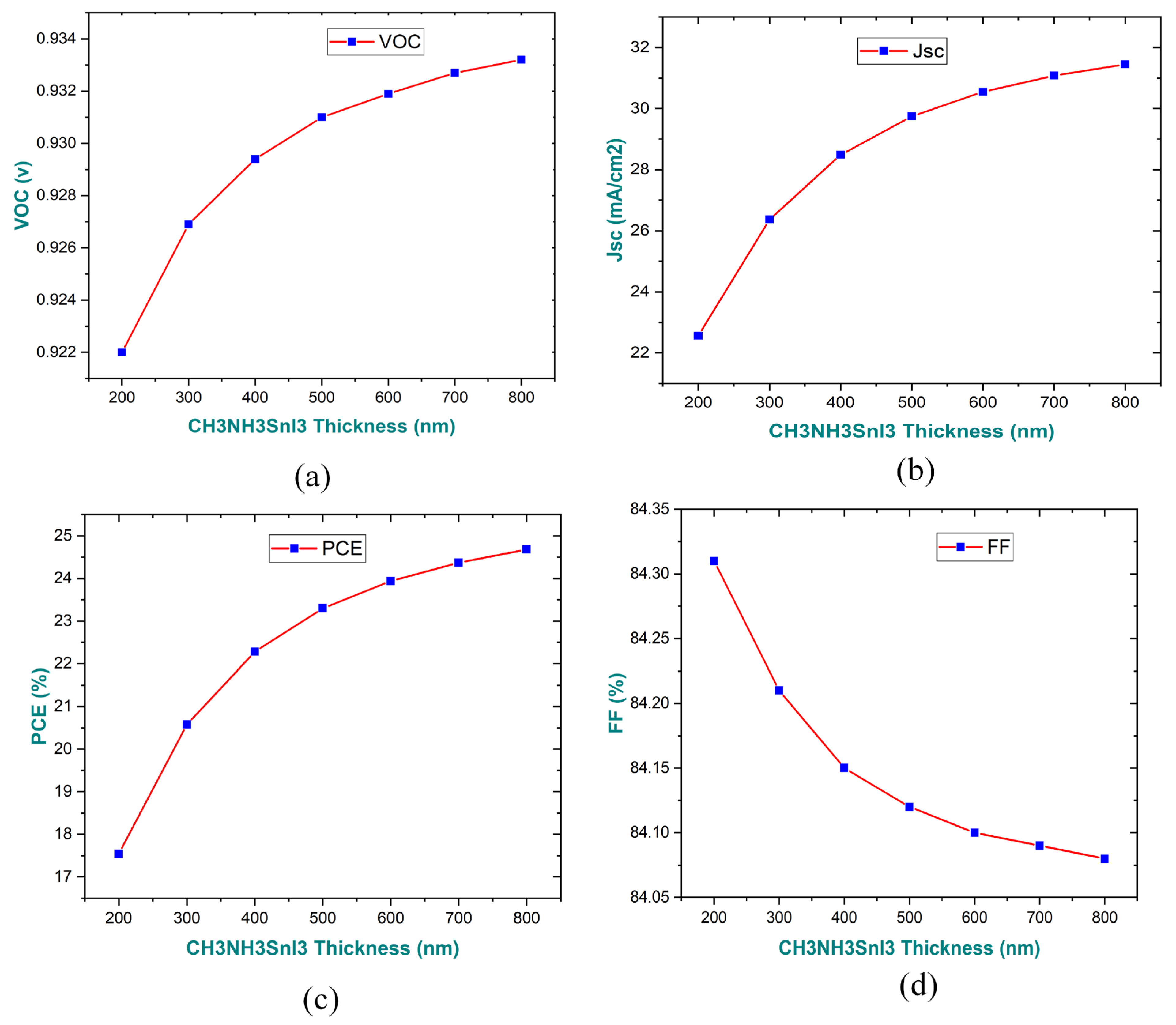
3.1. Impact of Absorber Layer Thickness on Performance Parameters
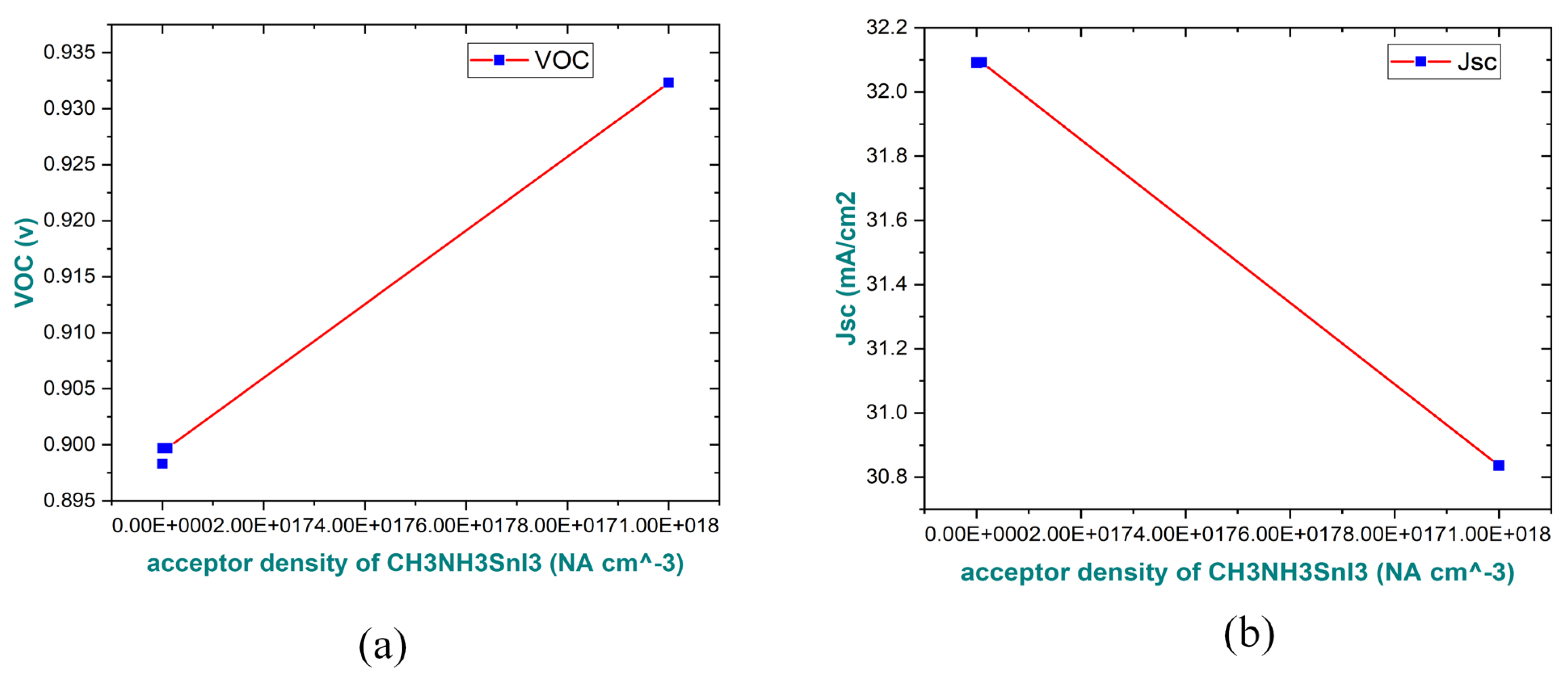
3.2. Impact on Doping Concentration (NA) of Absorber Layer on the Parameters of Performance
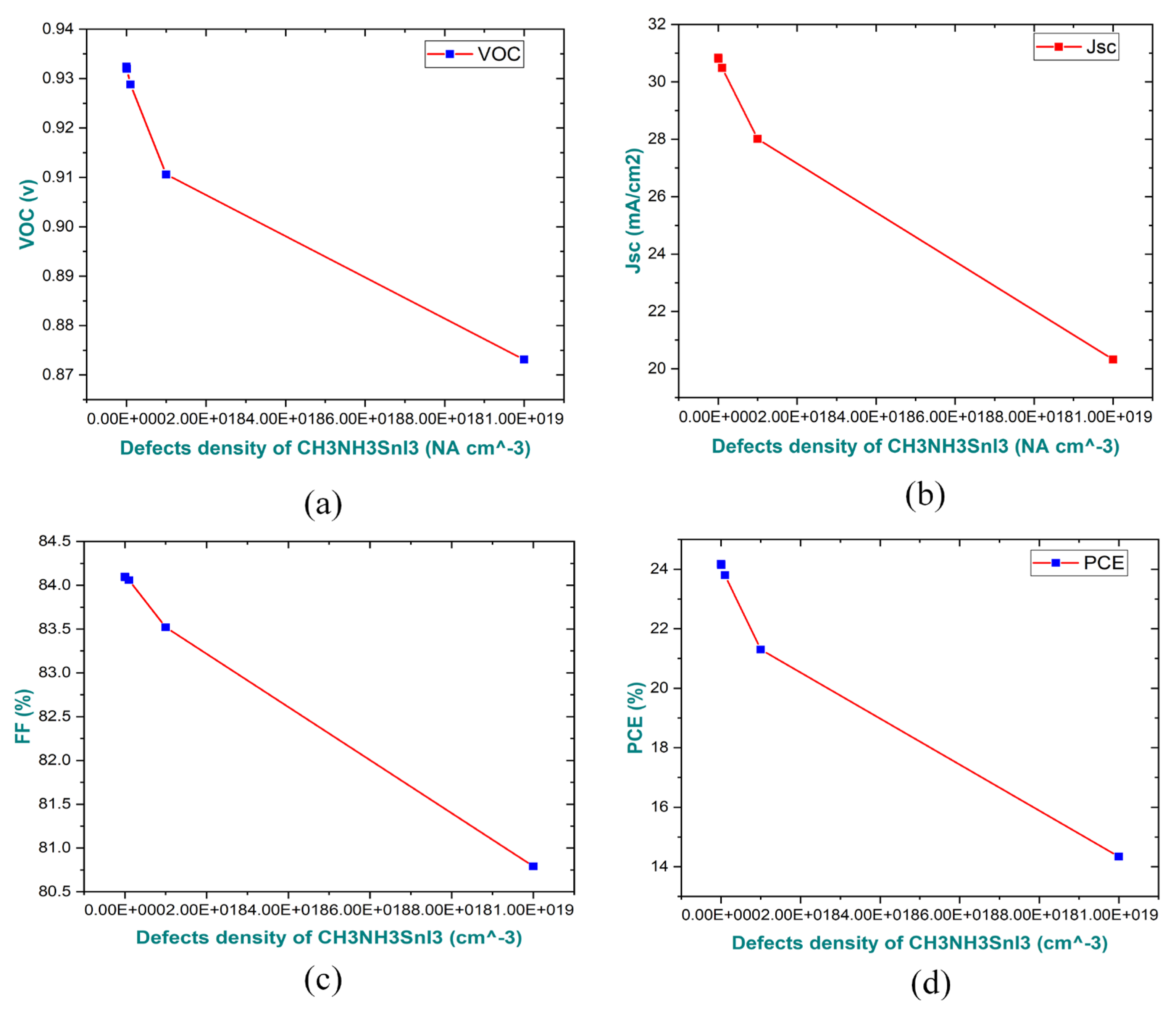
3.3. Impact on Absorber Layer Defect-Density NA on Parameters the Performance
3.4. Interfacing Defects state Analysis between ETL/Perovskite
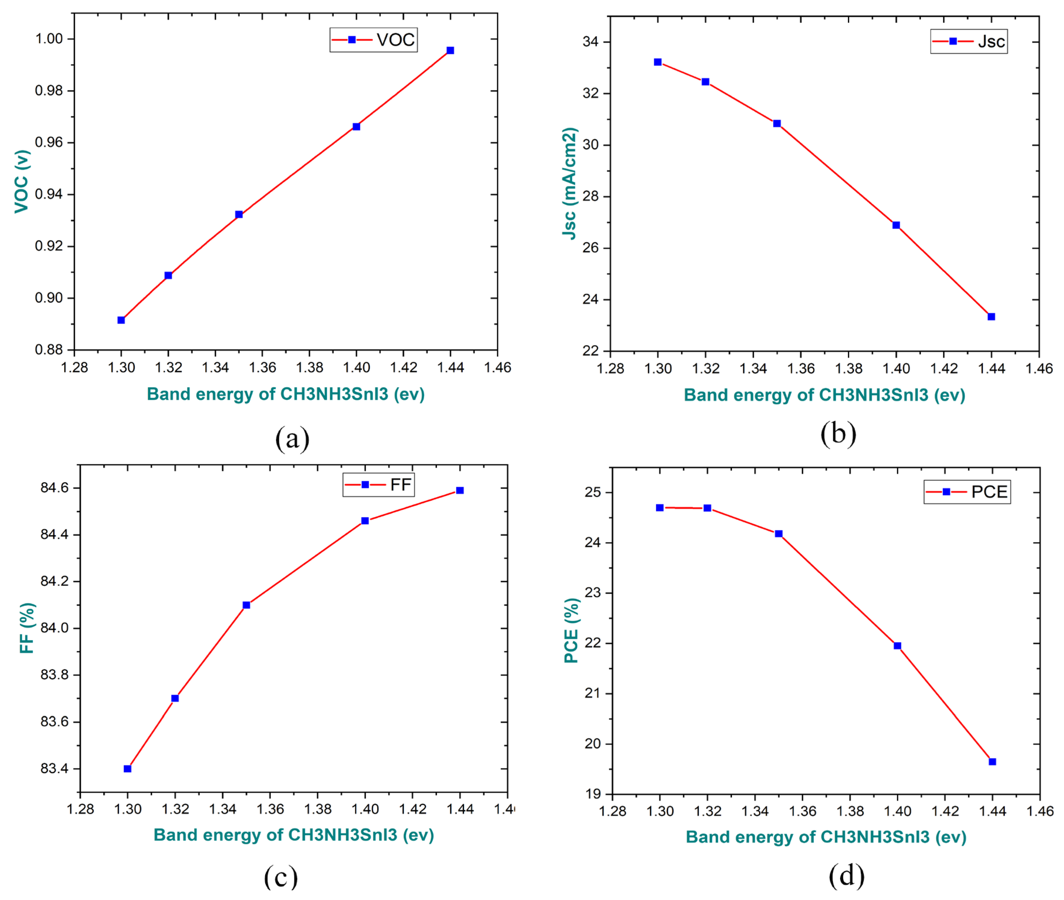
3.5. Impact of the Band Gap of the Absorber Layer on the Performance Parameters
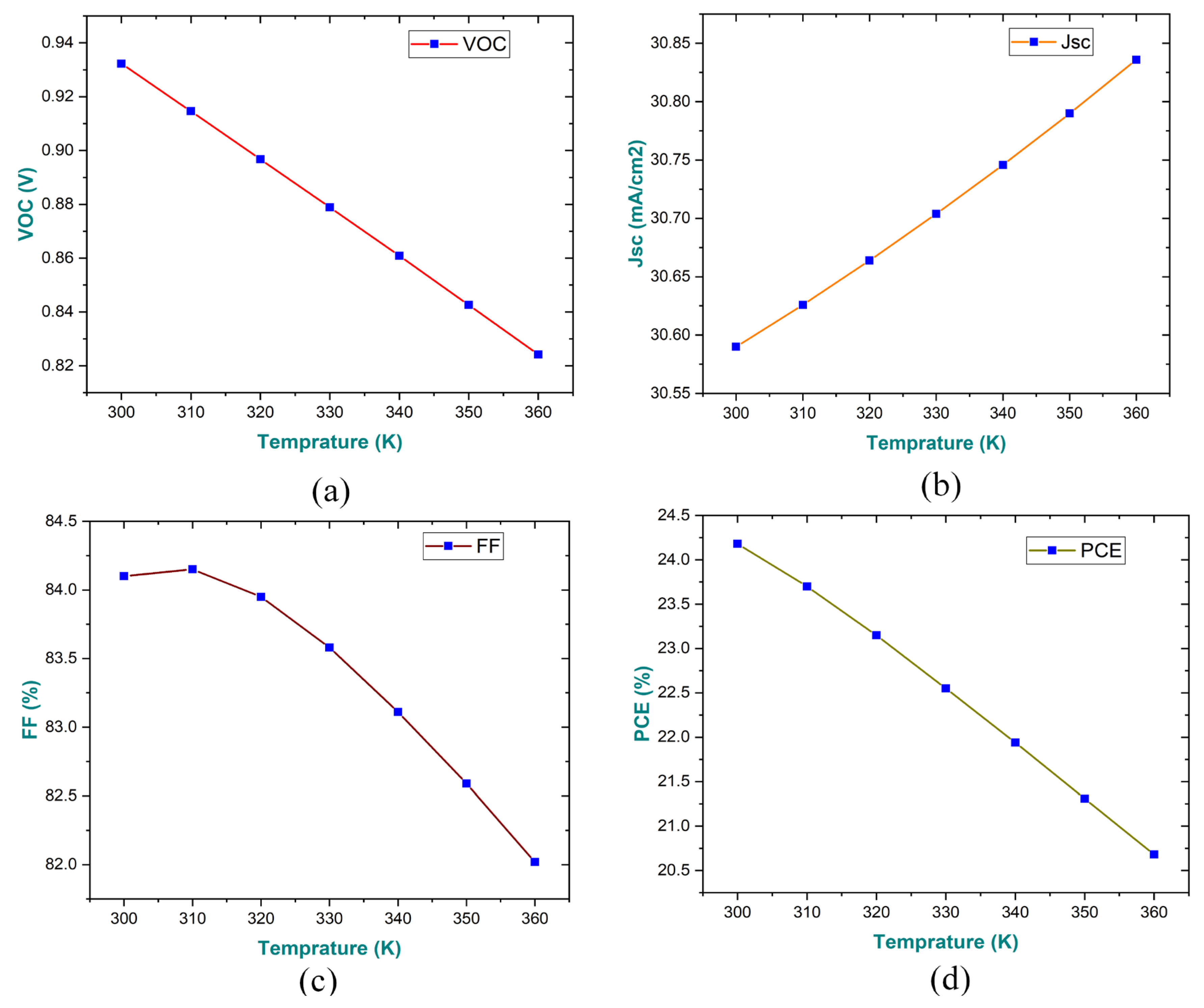
3.6. Impact of Temperature on Performance Parameters of the Device
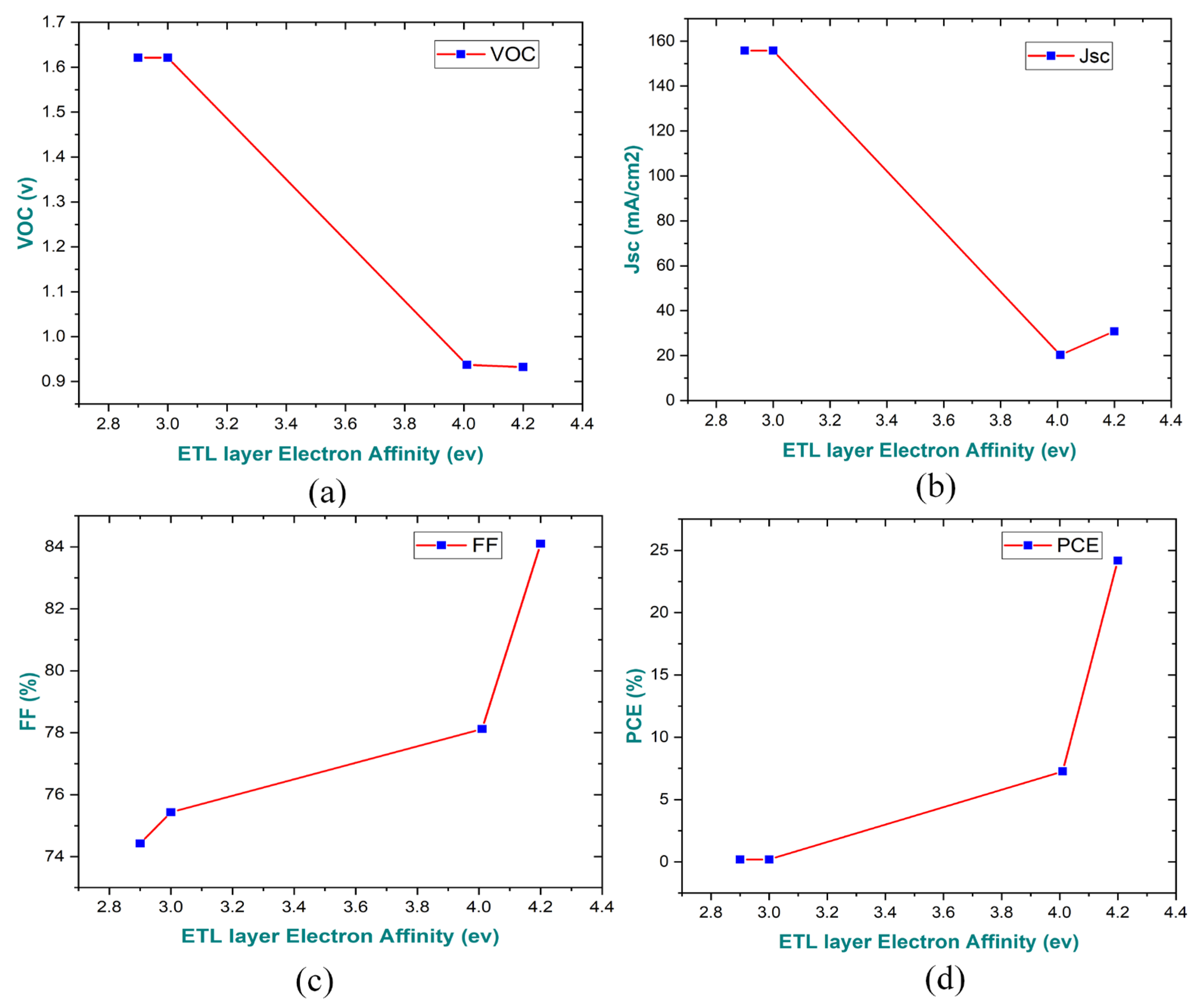
3.7. Impact on Electron Affinity of ETL on the Performance of the Parameter
3.8. Impact of Series (Rs) & Shunt Resistance (Rsh) on Performance Parameters
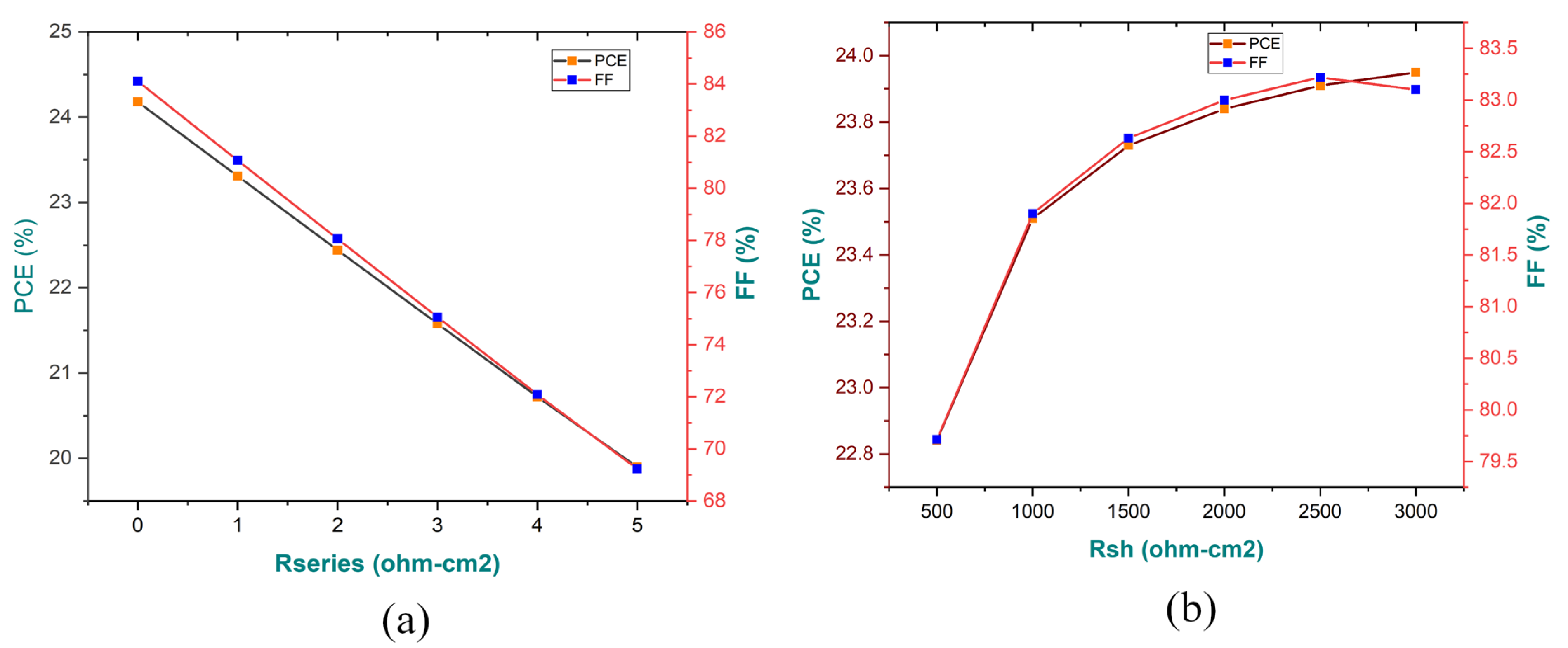
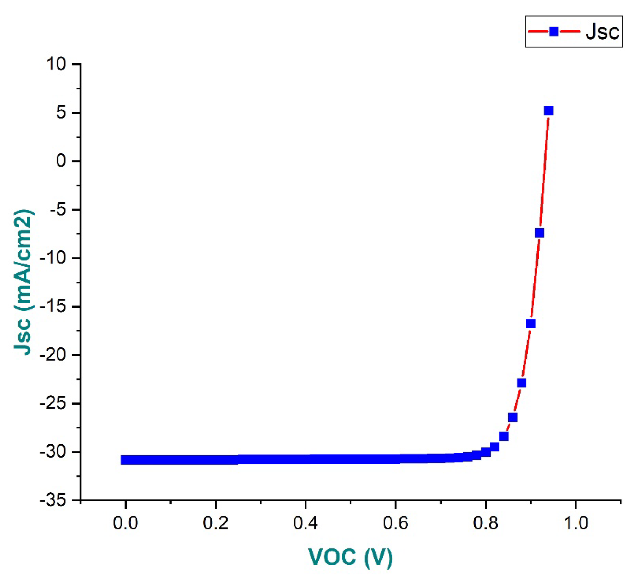
3.9. J-V Characteristics Analysis Curve
- Personal Consumption Expenditure at 24.18%
- Voltage of 0.928 V
- Current density of 30.898 mA/cm2
- Fill factor of 84.39%
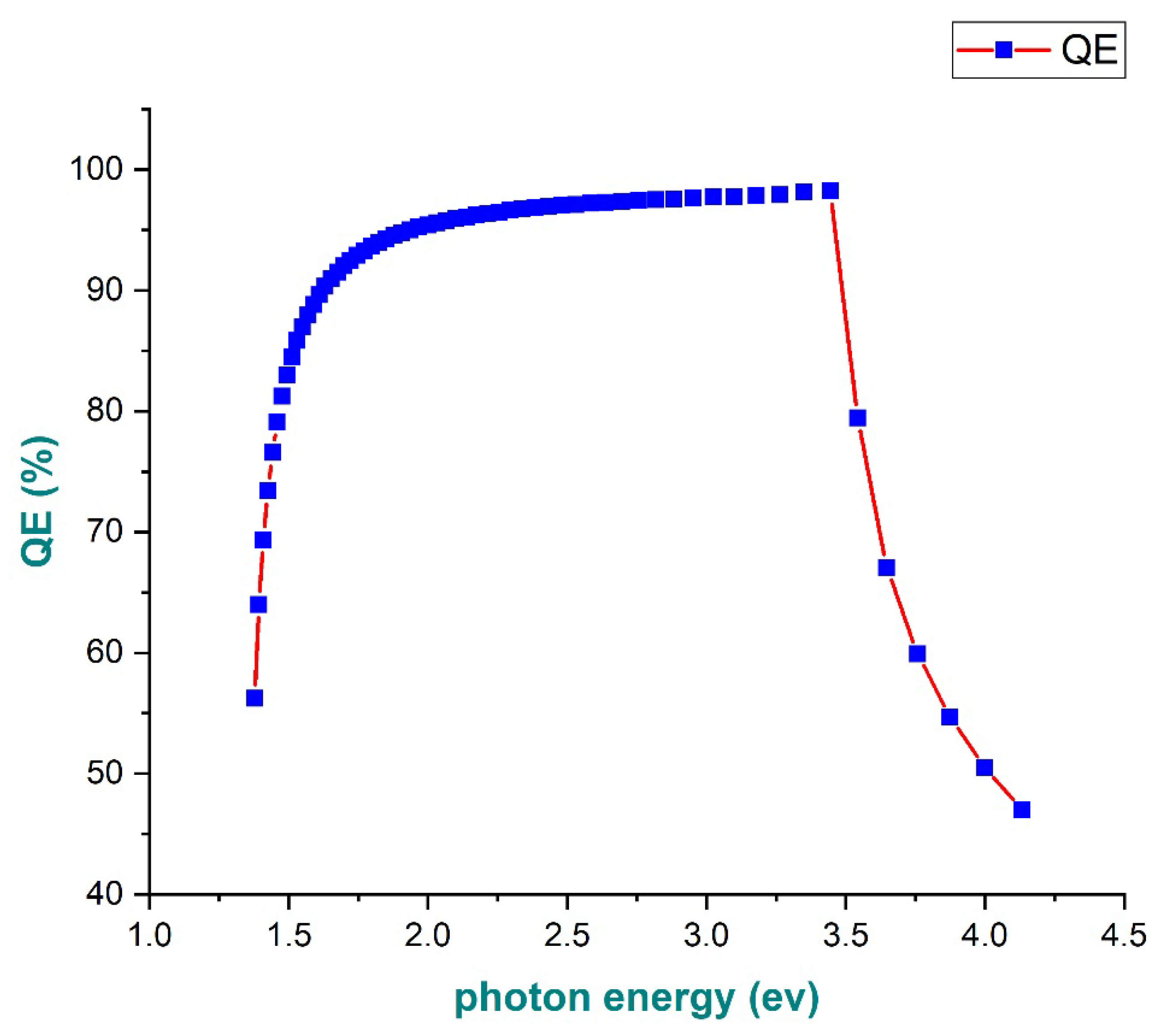
3.10. Evaluation of the Quantum Efficiency of Perovskite
4. Conclusion
Acknowledgments
References
- Yao, L. New Energy Utilization in Environmental Design and Realization. Energy Reports 2022, 8, 9211–9220. [CrossRef]
- Kamran, M.; Fazal, M.R.; Mudassar, M.; Ahmed, S.R.; Adnan, M.; Abid, I.; Randhawa, F.J.S.; Shams, H. Solar Photovoltaic Grid Parity: A Review of Issues and Challenges and Status of Different PV Markets. Int. J. Renew. Energy Res. 2019, 9, 244–260. [CrossRef]
- Shahid, H.; Kamran, M.; Mehmood, Z.; Saleem, M.Y.; Mudassar, M.; Haider, K. Implementation of the Novel Temperature Controller and Incremental Conductance MPPT Algorithm for Indoor Photovoltaic System. Sol. Energy 2018, 163, 235–242. [CrossRef]
- Kamran, M.; Mudassar, M.; Fazal, M.R.; Asghar, M.U.; Bilal, M.; Asghar, R. Implementation of Improved Perturb & Observe MPPT Technique with Confined Search Space for Standalone Photovoltaic System. J. King Saud Univ. - Eng. Sci. 2020, 32, 432–441. [CrossRef]
- Wang, J.; Xuan, Y.; Da, Y.; Xu, Y.; Zheng, L. Benefits of Photonic Management Strategy for Highly Efficient Bifacial Solar Cells. Opt. Commun. 2020, 462, 125358. [CrossRef]
- Ashraf, M.; Ayaz, M.; Khan, M.; Adil, S.F.; Farooq, W.; Ullah, N.; Nawaz Tahir, M. Recent Trends in Sustainable Solar Energy Conversion Technologies: Mechanisms, Prospects, and Challenges. Energy and Fuels 2023, 37, 6283–6301. [CrossRef]
- Hassan, Q.; Viktor, P.; J. Al-Musawi, T.; Mahmood Ali, B.; Algburi, S.; Alzoubi, H.M.; Khudhair Al-Jiboory, A.; Zuhair Sameen, A.; Salman, H.M.; Jaszczur, M. The Renewable Energy Role in the Global Energy Transformations. Renew. Energy Focus 2024, 48, 100545. [CrossRef]
- Nie, T.; Fang, Z.; Ren, X.; Duan, Y.; Liu, S. (Frank) Recent Advances in Wide-Bandgap Organic–Inorganic Halide Perovskite Solar Cells and Tandem Application. Nano-Micro Lett. 2023 151 2023, 15, 1–44. [CrossRef]
- Bati, A.S.R.; Zhong, Y.L.; Burn, P.L.; Nazeeruddin, M.K.; Shaw, P.E.; Batmunkh, M. Next-Generation Applications for Integrated Perovskite Solar Cells. Commun. Mater. 2023 41 2023, 4, 1–24. [CrossRef]
- Kumari, N.; Patel, S.R.; Gohel, J. V. Optical and Structural Properties of ZnO Thin Films Prepared by Spray Pyrolysis for Enhanced Efficiency Perovskite Solar Cell Application. Opt. Quantum Electron. 2018, 50. [CrossRef]
- Nykyruy, L.I.; Yavorskyi, R.S.; Zapukhlyak, Z.R.; Wisz, G.; Potera, P. Evaluation of CdS/CdTe Thin Film Solar Cells: SCAPS Thickness Simulation and Analysis of Optical Properties. Opt. Mater. (Amst). 2019, 92, 319–329. [CrossRef]
- Bimli, S.; Manjunath, V.; Mulani, S.R.; Miglani, A.; Game, O.S.; Devan, R.S. Theoretical Investigations of All Inorganic Cs2SnI6 Double Perovskite Solar Cells for Efficiency ~30%. Sol. Energy 2023, 256, 76–87. [CrossRef]
- Bati, A.S.R.; Sutanto, A.A.; Hao, M.; Batmunkh, M.; Yamauchi, Y.; Wang, L.; Wang, Y.; Nazeeruddin, M.K.; Shapter, J.G. Cesium-Doped Ti3C2Tx MXene for Efficient and Thermally Stable Perovskite Solar Cells. Cell Rep. Phys. Sci. 2021, 2, 100598. [CrossRef]
- Bati, A.S.R.; Hao, M.; Macdonald, T.J.; Batmunkh, M.; Yamauchi, Y.; Wang, L.; Shapter, J.G. 1D-2D Synergistic MXene-Nanotubes Hybrids for Efficient Perovskite Solar Cells. Small 2021, 17, 2101925. [CrossRef]
- Shaw, B.K.; Castillo-Blas, C.; Thorne, M.F.; Ríos Gómez, M.L.; Forrest, T.; Lopez, M.D.; Chater, P.A.; McHugh, L.N.; Keen, D.A.; Bennett, T.D. Principles of Melting in Hybrid Organic-Inorganic Perovskite and Polymorphic ABX3structures. Chem. Sci. 2022, 13, 2033–2042. [CrossRef]
- Wu, J.; Cha, H.; Du, T.; Dong, Y.; Xu, W.; Lin, C.T.; Durrant, J.R. A Comparison of Charge Carrier Dynamics in Organic and Perovskite Solar Cells. Adv. Mater. 2022, 34, 2101833. [CrossRef]
- Bati, A.S.R.; Yu, L.P.; Tawfik, S.A.; Spencer, M.J.S.; Shaw, P.E.; Batmunkh, M.; Shapter, J.G. Electrically Sorted Single-Walled Carbon Nanotubes-Based Electron Transporting Layers for Perovskite Solar Cells. iScience 2019, 14, 100–112. [CrossRef]
- Zhang, Y.; Kirs, A.; Ambroz, F.; Lin, C.T.; Bati, A.S.R.; Parkin, I.P.; Shapter, J.G.; Batmunkh, M.; Macdonald, T.J. Ambient Fabrication of Organic–Inorganic Hybrid Perovskite Solar Cells. Small Methods 2021, 5, 2000744. [CrossRef]
- Park, H.-J.; Son, H.; Jeong, B.-S. SCAPS-1D Simulation for Device Optimization to Improve Efficiency in Lead-Free CsSnI3 Perovskite Solar Cells. Inorganics 2024, Vol. 12, Page 123 2024, 12, 123. [CrossRef]
- Jung, H.S.; Han, G.S.; Park, N.G.; Ko, M.J. Flexible Perovskite Solar Cells. Joule 2019, 3, 1850–1880. [CrossRef]
- Goetz, K.P.; Taylor, A.D.; Hofstetter, Y.J.; Vaynzof, Y. Sustainability in Perovskite Solar Cells. ACS Appl. Mater. Interfaces 2021, 13, 1–17. [CrossRef]
- Liu, B.; Long, M.; Cai, M.Q.; Yang, J. Influence of the Number of Layers on Ultrathin CsSnI3 Perovskite: From Electronic Structure to Carrier Mobility. J. Phys. D. Appl. Phys. 2018, 51. [CrossRef]
- Gamal, N.; Sedky, S.H.; Shaker, A.; Fedawy, M. Design of Lead-Free Perovskite Solar Cell Using Zn1-XMgxO as ETL: SCAPS Device Simulation. Optik (Stuttg). 2021, 242. [CrossRef]
- Liu, C.; Li, W.; Zhang, C.; Ma, Y.; Fan, J.; Mai, Y. All-Inorganic CsPbI2Br Perovskite Solar Cells with High Efficiency Exceeding 13%. J. Am. Chem. Soc. 2018, 140, 3825–3828. [CrossRef]
- Giustino, F.; Snaith, H.J. Toward Lead-Free Perovskite Solar Cells. ACS Energy Lett. 2016, 1, 1233–1240. [CrossRef]
- Cao, J.; Yan, F. Recent Progress in Tin-Based Perovskite Solar Cells. Energy Environ. Sci. 2021, 14, 1286–1325. [CrossRef]
- Montecucco, R.; Quadrivi, E.; Po, R.; Grancini, G. All-Inorganic Cesium-Based Hybrid Perovskites for Efficient and Stable Solar Cells and Modules. Adv. Energy Mater. 2021, 11. [CrossRef]
- Li, B.; Di, H.; Chang, B.; Yin, R.; Fu, L.; Zhang, Y.N.; Yin, L. Efficient Passivation Strategy on Sn Related Defects for High Performance All-Inorganic CsSnI3 Perovskite Solar Cells. Adv. Funct. Mater. 2021, 31. [CrossRef]
- Chen, H.; Xiang, S.; Li, W.; Liu, H.; Zhu, L.; Yang, S. Inorganic Perovskite Solar Cells: A Rapidly Growing Field. Sol. RRL 2018, 2. [CrossRef]
- Roy, P.; Sinha, N.K.; Tiwari, S.; Khare, A. Influence of Defect Density and Layer Thickness of Absorption Layer on the Performance of Tin Based Perovskite Solar Cell. IOP Conf. Ser. Mater. Sci. Eng. 2020, 798. [CrossRef]
- Hossain, M.K.; Toki, G.F.I.; Kuddus, A.; Mohammed, M.K.A.; Pandey, R.; Madan, J.; Bhattarai, S.; Rahman, M.F.; Dwivedi, D.K.; Amami, M.; et al. Optimization of the Architecture of Lead-Free CsSnCl3-Perovskite Solar Cells for Enhancement of Efficiency: A Combination of SCAPS-1D and WxAMPS Study. Mater. Chem. Phys. 2023, 308. [CrossRef]
- Wang, N.; Zhou, Y.; Ju, M.G.; Garces, H.F.; Ding, T.; Pang, S.; Zeng, X.C.; Padture, N.P.; Sun, X.W. Heterojunction-Depleted Lead-Free Perovskite Solar Cells with Coarse-Grained B-γ-CsSnI3 Thin Films. Adv. Energy Mater. 2016, 6. [CrossRef]
- Lin, S.; Zhang, B.; Lü, T.Y.; Zheng, J.C.; Pan, H.; Chen, H.; Lin, C.; Li, X.; Zhou, J. Inorganic Lead-Free B-γ-CsSnI3Perovskite Solar Cells Using Diverse Electron-Transporting Materials: A Simulation Study. ACS Omega 2021, 6, 26689–26698. [CrossRef]
- Petrus, M.L.; Schlipf, J.; Li, C.; Gujar, T.P.; Giesbrecht, N.; Müller-Buschbaum, P.; Thelakkat, M.; Bein, T.; Hüttner, S.; Docampo, P. Capturing the Sun: A Review of the Challenges and Perspectives of Perovskite Solar Cells. Adv. Energy Mater. 2017, 7. [CrossRef]
- Li, Z.; Wang, R.; Xue, J.; Xing, X.; Yu, C.; Huang, T.; Chu, J.; Wang, K.L.; Dong, C.; Wei, Z.; et al. Core-Shell ZnO@SnO2 Nanoparticles for Efficient Inorganic Perovskite Solar Cells. J. Am. Chem. Soc. 2019, 141, 17610–17616. [CrossRef]
- Dunfield, S.P.; Bliss, L.; Zhang, F.; Luther, J.M.; Zhu, K.; van Hest, M.F.A.M.; Reese, M.O.; Berry, J.J. From Defects to Degradation: A Mechanistic Understanding of Degradation in Perovskite Solar Cell Devices and Modules. Adv. Energy Mater. 2020, 10. [CrossRef]
- Moustafa, M.; Alzoubi, T. Numerical Simulation of Single Junction Ingan Solar Cell by Scaps. Key Eng. Mater. 2019, 821 KEM, 407–413. [CrossRef]
- Zhang, J.; Hodes, G.; Jin, Z.; Liu, S. All-Inorganic CsPbX3 Perovskite Solar Cells: Progress and Prospects. Angew. Chemie - Int. Ed. 2019, 58, 15596–15618. [CrossRef]
- Fatima, Q.; Haidry, A.A.; Hussain, R.; Zhang, H. Device Simulation of a Thin-Layer CsSnI3-Based Solar Cell with Enhanced 31.09% Efficiency. Energy and Fuels 2023, 37, 7411–7423. [CrossRef]
- Ansari, M.I.H.; Qurashi, A.; Nazeeruddin, M.K. Frontiers, Opportunities, and Challenges in Perovskite Solar Cells: A Critical Review. J. Photochem. Photobiol. C Photochem. Rev. 2018, 35, 1–24. [CrossRef]

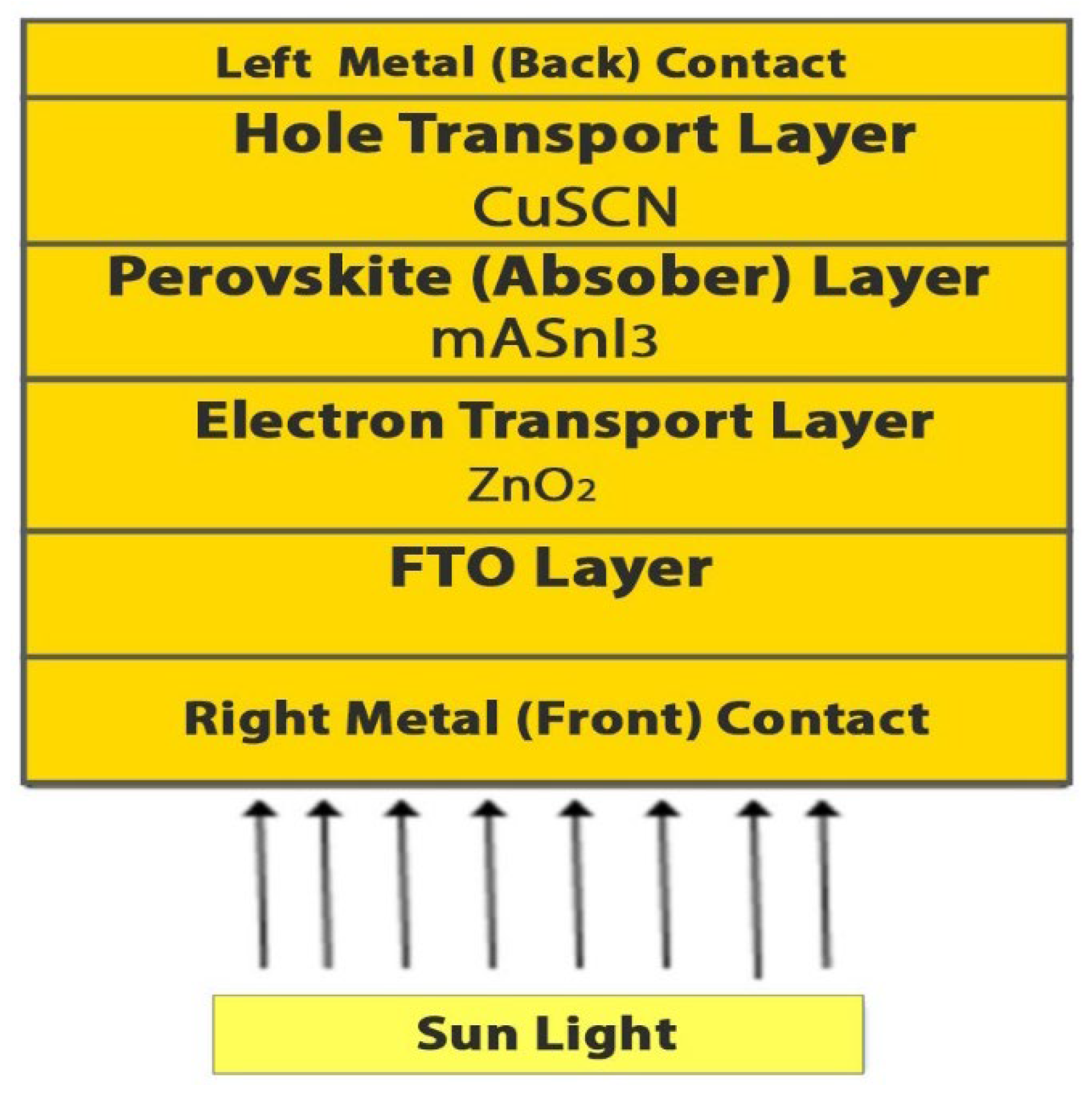



| Parameters | FTO | ZnO | CH3NH3SnI3 | CuSCN |
|---|---|---|---|---|
| Thickness (nm) | 400 | 50 | 650 | 150 |
| Electron affinity(eV) | 4.00 | 4.200 | 4.170 | 2.200 |
| Bandgap(eV) | 3.500 | 3.260 | 1.350 | 3.400 |
| CB effective density (cm-3) | 2.2 X 10¹⁸ | 2.2 X 10¹⁸ | 2.2 X 10¹⁸ | 1.7 X 10¹⁹ |
| Dielectric permittivity (Er) VB effective density state (cm-3) Hole mobility up (cm2/Vs) Thermal velocity of Hole (cm/s) Thermal velocity of Electron (cm/s) Acceptor density NA (cm-3) Donor density ND(cm-3) Density of Defect NA (cm3) |
9.000 1.8 X 10¹⁸ 1.0 X 101 1.0 X 10⁷ 2.0 X 101 0.0 X 100 1.0 X 10¹⁹ 1.0 X 10¹⁵ |
10.000 1.8 X 10¹⁸ 1.0 X 10⁷ 1.0 X 10⁷ 1.0 X 10⁷ 0.0 X 100 1.0 X 10¹⁷ 1.0 X 10¹⁵ |
8.200 1.8 X 10¹⁸ 3.0 X 10² 1.0 X 10⁷ 1.0 X 10⁷ 1.0 X 101 0.0 X 100 1.0 X 10¹⁵ |
10.000 2.5X 10²¹ 1.0X 10⁻¹ 1.0 X 10⁷ 1.0 X 10⁷ 1.0 X 10¹⁸ 0.0 X 100 1.0 X 10¹⁵ |
Disclaimer/Publisher’s Note: The statements, opinions and data contained in all publications are solely those of the individual author(s) and contributor(s) and not of MDPI and/or the editor(s). MDPI and/or the editor(s) disclaim responsibility for any injury to people or property resulting from any ideas, methods, instructions or products referred to in the content. |
© 2024 by the authors. Licensee MDPI, Basel, Switzerland. This article is an open access article distributed under the terms and conditions of the Creative Commons Attribution (CC BY) license (http://creativecommons.org/licenses/by/4.0/).


