Submitted:
14 June 2024
Posted:
17 June 2024
You are already at the latest version
Abstract
Keywords:
1. Introduction
2. Experimental Techniques
2.1. Chemicals
2.2. Constructing CAZTS Layers
2.3. Characterization and Measurements
3. Results and Discussion
3.1. EDX and Structural Studies
3.2. Morphological Properties
3.3. Raman Spectra
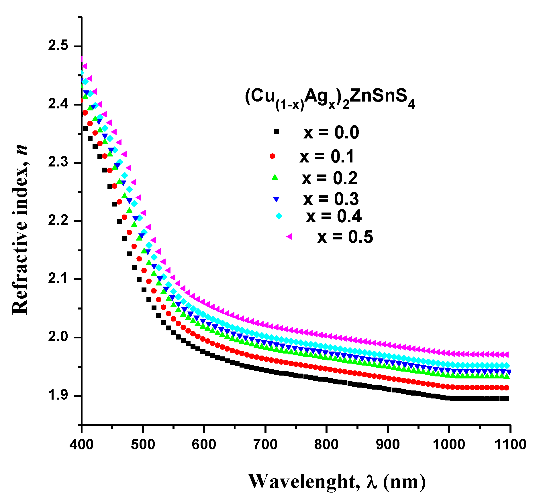
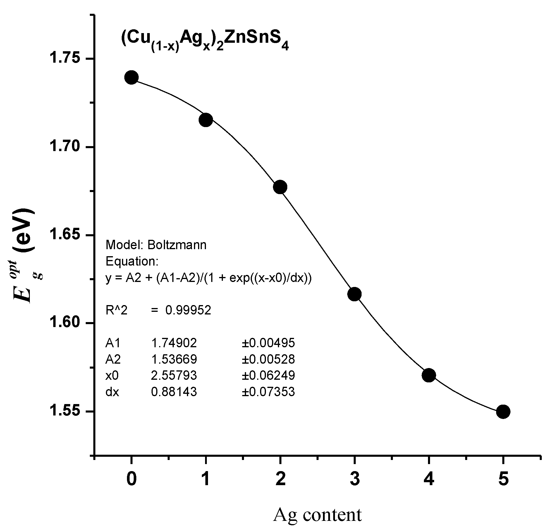
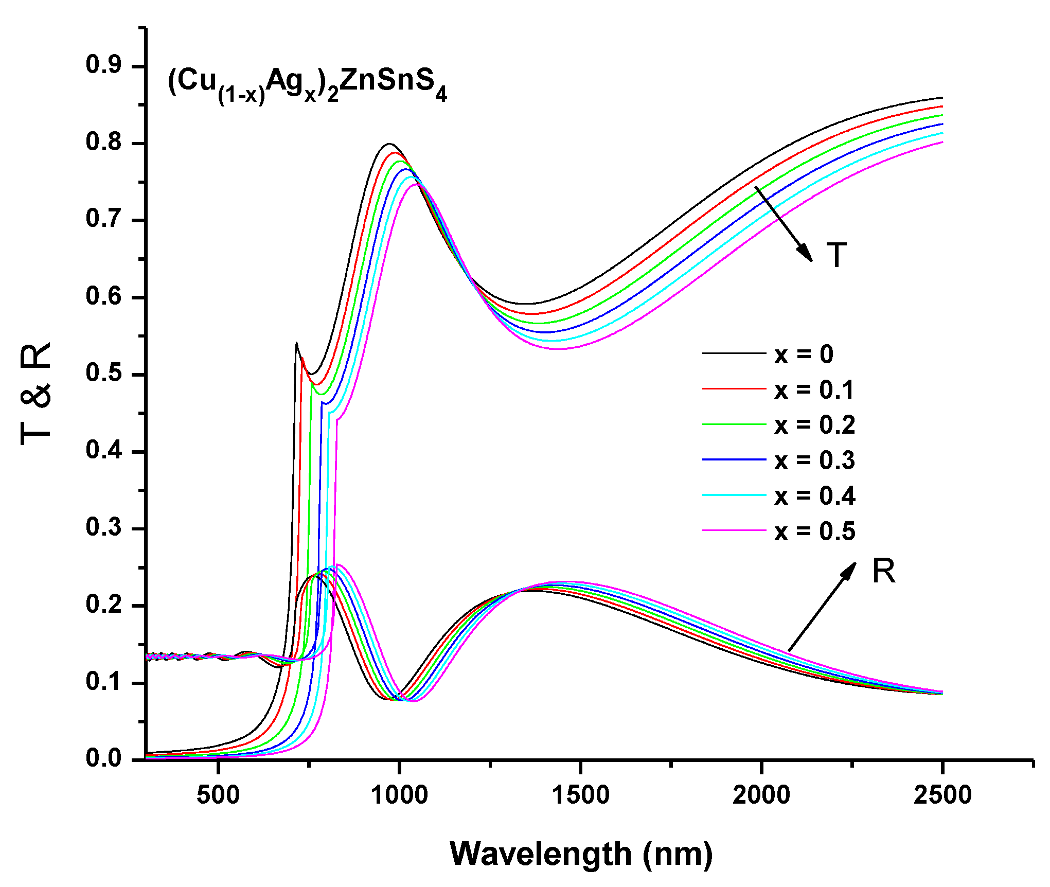
3.4. Spectroscopic Ellipsometry
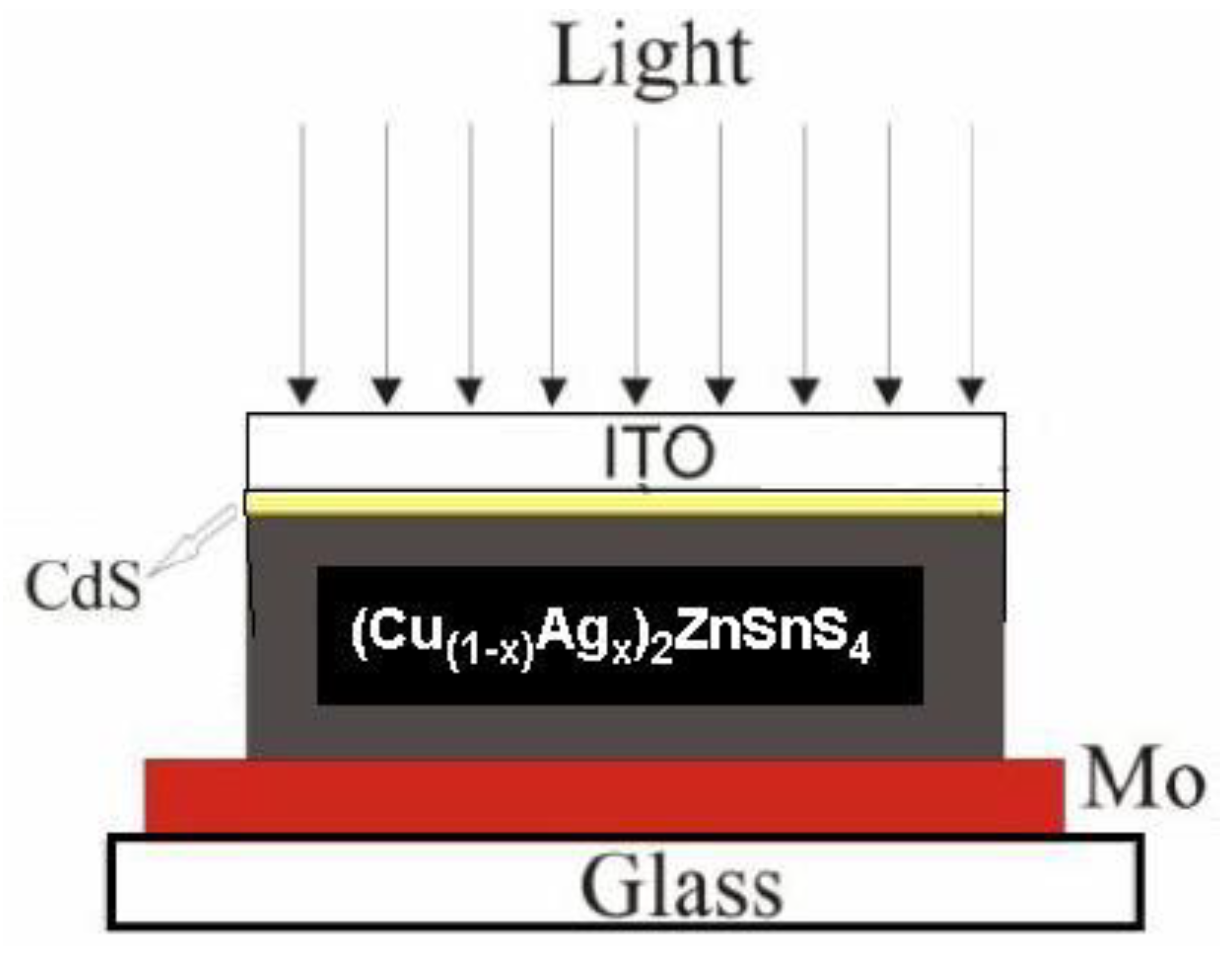
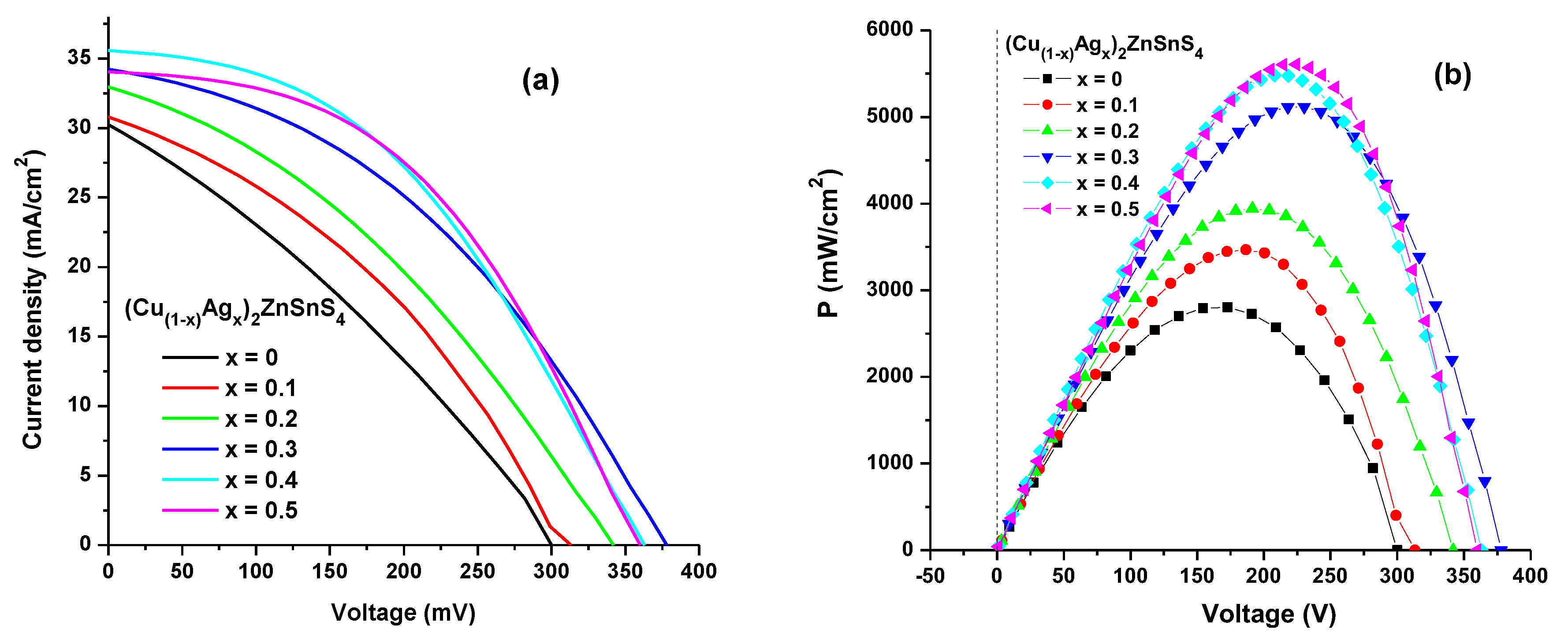
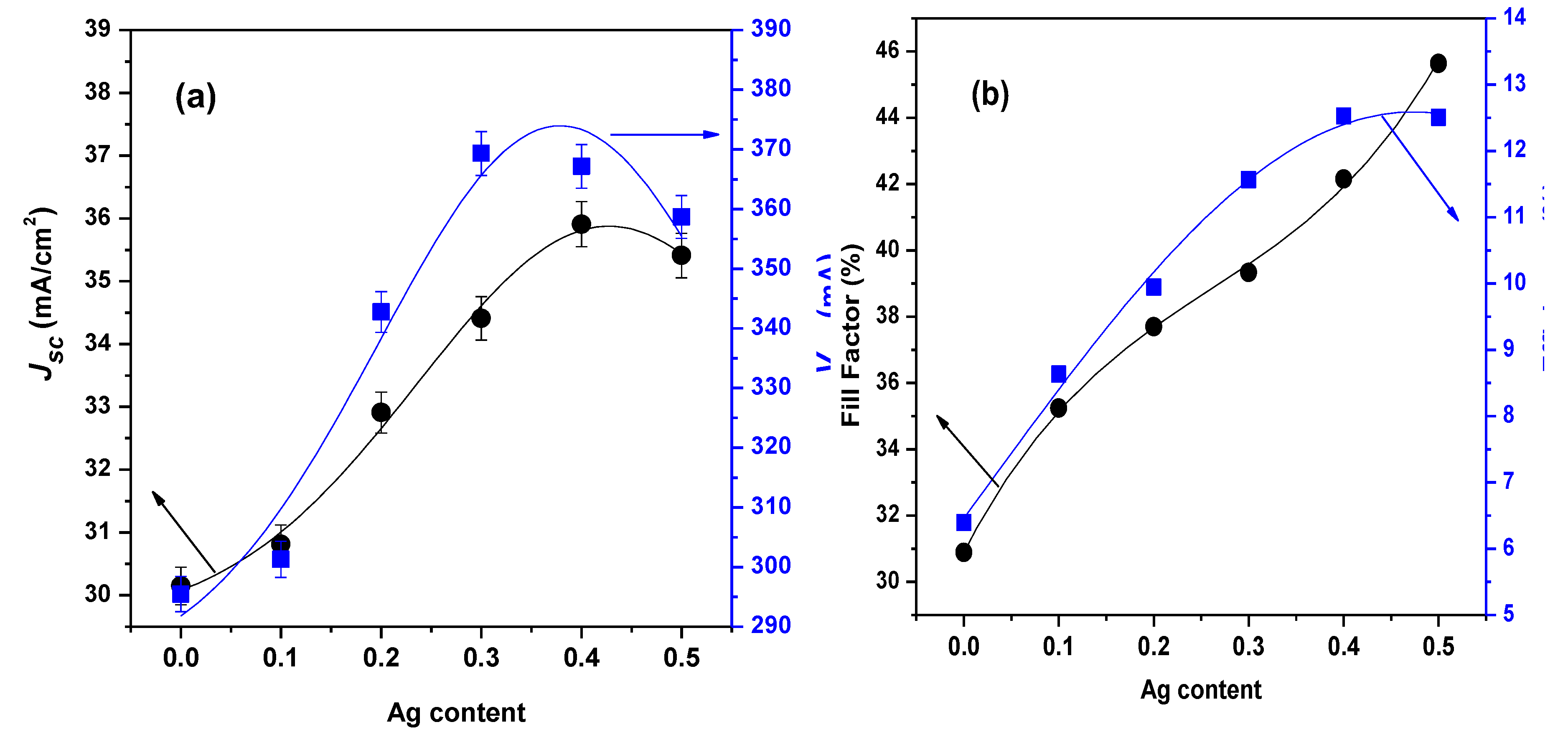
3.5. Features of p-n Junction
4. Conclusions
Acknowledgments
References
- Mitzi, David B., Min Yuan, Wei Liu, Andrew J. Kellock, S. Jay Chey, Vaughn Deline, and Alex G. Schrott. "A high-efficiency solution-deposited thin-film photovoltaic device." Advanced Materials 20, no. 19 (2008): 3657-3662. [CrossRef]
- Nguyen, Thi Hiep, Takato Kawaguchi, Jakapan Chantana, Takashi Minemoto, Takashi Harada, Shuji Nakanishi, and Shigeru Ikeda. "Structural and Solar Cell Properties of a Ag-Containing Cu2ZnSnS4 Thin Film Derived from Spray Pyrolysis." ACS applied materials & interfaces 10, no. 6 (2018): 5455-5463. [CrossRef]
- Bär, M., I. Repins, M. A. Contreras, L. Weinhardt, R. Noufi, and C. Heske. "Chemical and electronic surface structure of 20%-efficient Cu (In, Ga) Se 2 thin film solar cell absorbers." Applied Physics Letters 95, no. 5 (2009): 05210. [CrossRef]
- Sun, Rujun, Daming Zhuang, Ming Zhao, Qianming Gong, Mike Scarpulla, Yaowei Wei, Guoan Ren, and Yixuan Wu. "Beyond 11% efficient Cu2ZnSn (Se, S) 4 thin film solar cells by cadmium alloying." Solar Energy Materials and Solar Cells 174 (2018): 494-498. [CrossRef]
- Todorov, Teodor K., Kathleen B. Reuter, and David B. Mitzi. "High-efficiency solar cell with earth-abundant liquid-processed absorber." Advanced materials 22, no. 20 (2010): E156-E159. [CrossRef]
- Fernandes, P. A. , Salomé, P. M. P., & Da Cunha, A. F., CuxSnSx+ 1 (x= 2, 3) thin films grown by sulfurization of metallic precursors deposited by dc magnetron sputtering. physica status solidi c, 7 (2010) 901-904. [CrossRef]
- Sun, R. , et al., Beyond 11% efficient Cu 2 ZnSn (Se, S) 4 thin film solar cells by cadmium alloying. Solar Energy Materials and Solar Cells, 2018. 174: p. 494-498. [CrossRef]
- Lee, Seul Gi, Jongmin Kim, Huyn Suk Woo, Yongcheol Jo, A. I. Inamdar, S. M. Pawar, Hyung Sang Kim, Woong Jung, and Hyun Sik Im. "Structural, morphological, compositional, and optical properties of single step electrodeposited Cu2ZnSnS4 (CZTS) thin films for solar cell application." Current Applied Physics 14, no. 3 (2014): 254-258. [CrossRef]
- Lincot, Daniel, Jean-François Guillemoles, S. Taunier, D. Guimard, J. Sicx-Kurdi, A. Chaumont, O. Roussel et al. "Chalcopyrite thin film solar cells by electrodeposition." Solar Energy 77, no. 6 (2004): 725-737. [CrossRef]
- Cunningham, D., M. Rubcich, and D. Skinner. "Cadmium telluride PV module manufacturing at BP Solar." Progress in Photovoltaics: Research and Applications 10, no. 2 (2002): 159-168. [CrossRef]
- Ahmed, Shafaat, Kathleen B. Reuter, Oki Gunawan, Lian Guo, Lubomyr T. Romankiw, and Hariklia Deligianni. "A high efficiency electrodeposited Cu2ZnSnS4 solar cell." Advanced Energy Materials 2, no. 2 (2012): 253-259. [CrossRef]
- Farinella, Marta, Rosalinda Inguanta, Tiziana Spanò, P. Livreri, S. Piazza, and C. Sunseri. "Electrochemical deposition of CZTS thin films on flexible substrate." Energy Procedia 44 (2014): 105-110. [CrossRef]
- Ge, Jie, and Yanfa Yan. "Controllable multinary alloy electrodeposition for thin-film solar cell fabrication: a case study of kesterite Cu2ZnSnS4." iScience 1 (2018): 55-71. [CrossRef]
- Schäfer, W. , and Rudolf Nitsche. "Tetrahedral quaternary chalcogenides of the type Cu2 II IV S4 (Se4)." Materials Research Bulletin 9, no. 5 (1974): 645-654. [CrossRef]
- Wang, K., O. Gunawan, T. Todorov, B. Shin, S. J. Chey, N. A. Bojarczuk, D. Mitzi, and S. Guha. "Thermally evaporated Cu 2 ZnSnS 4 solar cells." Applied Physics Letters 97, no. 14 (2010): 143508. [CrossRef]
- Shin, Byungha, Oki Gunawan, Yu Zhu, Nestor A. Bojarczuk, S. Jay Chey, and Supratik Guha. "Thin film solar cell with 8.4% power conversion efficiency using an earth-abundant Cu2ZnSnS4 absorber." Progress in Photovoltaics: Research and Applications 21, no. 1 (2013): 72-76. [CrossRef]
- Tiwari, Kunal J., Raju Chetty, Ramesh Chandra Mallik, and P. Malar. "Solid state synthesis and e-beam evaporation growth of Cu2ZnSnSe4 for solar energy absorber applications." Solar Energy 153 (2017): 173-180. [CrossRef]
- Katagiri, Hironori, Kazuo Jimbo, Satoru Yamada, Tsuyoshi Kamimura, Win Shwe Maw, Tatsuo Fukano, Tadashi Ito, and Tomoyoshi Motohiro. "Enhanced conversion efficiencies of Cu2ZnSnS4-based thin film solar cells by using preferential etching technique." Applied physics express 1, no. 4 (2008): 041201. [CrossRef]
- Jimbo, Kazuo, Ryoichi Kimura, Tsuyoshi Kamimura, Satoru Yamada, Win Shwe Maw, Hideaki Araki, Koichiro Oishi, and Hironori Katagiri. "Cu2ZnSnS4-type thin film solar cells using abundant materials." Thin solid films 515, no. 15 (2007): 5997-5999. [CrossRef]
- Seboui, Zeineb, Yvan Cuminal, and Najoua Kamoun-Turki. "Physical properties of Cu2ZnSnS4 thin films deposited by spray pyrolysis technique." Journal of Renewable and Sustainable Energy 5, no. 2 (2013): 023113. [CrossRef]
- Hong, Chang Woo, Seung Wook Shin, Mahesh P. Suryawanshi, Myeng Gil Gang, Jaeyeong Heo, and Jin Hyeok Kim. "Chemically deposited CdS buffer/kesterite Cu2ZnSnS4 solar cells: relationship between CdS thickness and device performance." ACS applied materials & interfaces 9, no. 42 (2017): 36733-36744. [CrossRef]
- Nguyen, Thi Hiep, Takato Kawaguchi, Jakapan Chantana, Takashi Minemoto, Takashi Harada, Shuji Nakanishi, and Shigeru Ikeda. "Structural and Solar Cell Properties of a Ag-Containing Cu2ZnSnS4 Thin Film Derived from Spray Pyrolysis." ACS applied materials & interfaces 10, no. 6 (2018): 5455-5463. [CrossRef]
- Cazzaniga, Andrea, Andrea Crovetto, Chang Yan, Kaiwen Sun, Xiaojing Hao, Joan Ramis Estelrich, Stela Canulescu et al. "Ultra-thin Cu2ZnSnS4 solar cell by pulsed laser deposition." Solar Energy Materials and Solar Cells 166 (2017): 91-99. [CrossRef]
- Moholkar, A. V., S. S. Shinde, A. R. Babar, Kyu-Ung Sim, Ye-bin Kwon, K. Y. Rajpure, P. S. Patil, C. H. Bhosale, and J. H. Kim. "Development of CZTS thin films solar cells by pulsed laser deposition: influence of pulse repetition rate." Solar Energy 85, no. 7 (2011): 1354-1363. [CrossRef]
- Lokhande, A. C., R. B. V. Chalapathy, J. S. Jang, P. T. Babar, M. G. Gang, C. D. Lokhande, and Jin Hyeok Kim. "Fabrication of pulsed laser deposited Ge doped CZTSSe thin film based solar cells: Influence of selenization treatment." Solar Energy Materials and Solar Cells 161 (2017): 355-367. [CrossRef]
- Agawane, G. L., S. A. Vanalakar, A. S. Kamble, A. V. Moholkar, and J. H. Kim. "Fabrication of Cu2 (ZnxMg1-x) SnS4 thin films by pulsed laser deposition technique for solar cell applications." Materials Science in Semiconductor Processing 76 (2018): 50-54. [CrossRef]
- Guo, Qijie, Grayson M. Ford, Wei-Chang Yang, Bryce C. Walker, Eric A. Stach, Hugh W. Hillhouse, and Rakesh Agrawal. "Fabrication of 7.2% efficient CZTSSe solar cells using CZTS nanocrystals." Journal of the American Chemical Society 132, no. 49 (2010): 17384-17386. [CrossRef]
- Kim, Jongmin, C. Park, S. M. Pawar, Akbar I. Inamdar, Yongcheol Jo, J. Han, JinPyo Hong et al. "Optimization of sputtered ZnS buffer for Cu2ZnSnS4 thin film solar cells." Thin Solid Films 566 (2014): 88-92. [CrossRef]
- Barkhouse, D. Aaron R., Oki Gunawan, Tayfun Gokmen, Teodor K. Todorov, and David B. Mitzi. "Device characteristics of a 10.1% hydrazine-processed Cu2ZnSn (Se, S) 4 solar cell." Progress in Photovoltaics: Research and Applications 20, no. 1 (2012): 6-11. [CrossRef]
- Wang, Wei, Mark T. Winkler, Oki Gunawan, Tayfun Gokmen, Teodor K. Todorov, Yu Zhu, and David B. Mitzi. "Device characteristics of CZTSSe thin-film solar cells with 12.6% efficiency." Advanced Energy Materials 4, no. 7 (2014): 1301465. [CrossRef]
- Lee, Seul Gi, Jongmin Kim, Huyn Suk Woo, Yongcheol Jo, A. I. Inamdar, S. M. Pawar, Hyung Sang Kim, Woong Jung, and Hyun Sik Im. "Structural, morphological, compositional, and optical properties of single step electrodeposited Cu2ZnSnS4 (CZTS) thin films for solar cell application." Current Applied Physics 14, no. 3 (2014): 254-258. [CrossRef]
- Sun, R. , et al., Beyond 11% efficient Cu 2 ZnSn (Se, S) 4 thin film solar cells by cadmium alloying. Solar Energy Materials and Solar Cells, 2018. 174: p. 494-498. [CrossRef]
- Sun, Kaiwen, Fangyang Liu, Chang Yan, Fangzhou Zhou, Jialiang Huang, Yansong Shen, Rong Liu, and Xiaojing Hao. "Influence of sodium incorporation on kesterite Cu2ZnSnS4 solar cells fabricated on stainless steel substrates." Solar Energy Materials and Solar Cells 157 (2016): 565-571. [CrossRef]
- Liu, Xu, Jialiang Huang, Fangzhou Zhou, Fangyang Liu, Kaiwen Sun, Chang Yan, John A. Stride, and Xiaojing Hao. "Understanding the key factors of enhancing phase and compositional controllability for 6% efficient pure-sulfide Cu2ZnSnS4 solar cells prepared from quaternary wurtzite nanocrystals." Chemistry of Materials 28, no. 11 (2016): 3649-3658. [CrossRef]
- Ericson, Tove, Fredrik Larsson, Tobias Törndahl, Christopher Frisk, Jes Larsen, Volodymyr Kosyak, Carl Hägglund, Shuyi Li, and Charlotte Platzer-Björkman. "Zinc-Tin-Oxide Buffer Layer and Low Temperature Post Annealing Resulting in a 9.0% Efficient Cd-Free Cu2ZnSnS4 Solar Cell." Solar RRL 1, no. 5 (2017): 1700001. [CrossRef]
- Hong, Chang Woo, Seung Wook Shin, Mahesh P. Suryawanshi, Myeng Gil Gang, Jaeyeong Heo, and Jin Hyeok Kim. "Chemically deposited CdS buffer/kesterite Cu2ZnSnS4 solar cells: relationship between CdS thickness and device performance." ACS applied materials & interfaces 9, no. 42 (2017): 36733-36744. [CrossRef]
- Erkan, Mehmet Eray, Vardaan Chawla, and Michael A. Scarpulla. "Reduced defect density at the CZTSSe/CdS interface by atomic layer deposition of Al2O3." Journal of Applied Physics 119, no. 19 (2016): 194504. [CrossRef]
- Crovetto, Andrea, Chang Yan, Beniamino Iandolo, Fangzhou Zhou, John Stride, Jørgen Schou, Xiaojing Hao, and Ole Hansen. "Lattice-matched Cu2ZnSnS4/CeO2 solar cell with open circuit voltage boost." Applied Physics Letters 109, no. 23 (2016): 233904. [CrossRef]
- Messaoud, Khaled Ben, Marie Buffière, Guy Brammertz, Nick Lenaers, Hans-Gerd Boyen, Sylvester Sahayaraj, Marc Meuris, Mosbah Amlouk, and Jef Poortmans. "Synthesis and characterization of (Cd, Zn) S buffer layer for Cu2ZnSnSe4 solar cells." Journal of Physics D: Applied Physics 50, no. 28 (2017): 285501. [CrossRef]
- Li, Jianjun, Xiaoru Liu, Wei Liu, Li Wu, Binghui Ge, Shuping Lin, Shoushuai Gao et al. "Restraining the Band Fluctuation of CBD-Zn (O, S) Layer: Modifying the Hetero-Junction Interface for High Performance Cu2ZnSnSe4 Solar Cells with Cd-Free Buffer Layer." Solar Rrl 1, no. 10 (2017): 1700075. [CrossRef]
- Bras, Patrice, and Jan Sterner. "Influence of H2S annealing and buffer layer on CZTS solar cells sputtered from a quaternary compound target." In 2014 IEEE 40th Photovoltaic Specialist Conference (PVSC), pp. 0328-0331. IEEE, 2014. [CrossRef]
- Nagoya, A., R. Asahi, and G. Kresse. "First-principles study of Cu2ZnSnS4 and the related band offsets for photovoltaic applications." Journal of Physics: Condensed Matter 23, no. 40 (2011): 404203. [CrossRef]
- Akram, Muhammad Aftab, Sofia Javed, Mohammad Islam, Mohammad Mujahid, and Amna Safdar. "Arrays of CZTS sensitized ZnO/ZnS and ZnO/ZnSe core/shell nanorods for liquid junction nanowire solar cells." Solar Energy Materials and Solar Cells 146 (2016): 121-128. [CrossRef]
- Qasem, A. , Hassan, A. A., Rajhi, F. Y., Abbas, H. A. S., & Shaaban, E. R. (2022). Effective role of cadmium doping in controlling the linear and non-linear optical properties of non-crystalline Cd–Se–S thin films. Journal of Materials Science: Materials in Electronics, 33(4), 1953-1965. [CrossRef]
- Sun, Kaiwen, Chang Yan, Fangyang Liu, Jialiang Huang, Fangzhou Zhou, John A. Stride, Martin Green, and Xiaojing Hao. "Over 9% efficient kesterite Cu2ZnSnS4 solar cell fabricated by using Zn1–xCdxS buffer layer." Advanced Energy Materials 6, no. 12 (2016): 1600046. [CrossRef]
- Qasem, A. , Alshahrani, B., Yakout, H. A., Abbas, H. A. S., & Shaaban, E. R. (2021). Tuning structural, optical, electrical and photovoltaic characteristics of n-type CdS1− xSbx layers for optimizing the performance of n-(CdS: Sb)/p-Si solar cells. Applied Physics A, 127(11), 1-13. [CrossRef]
- Yan, Chang, Fangyang Liu, Kaiwen Sun, Ning Song, John A. Stride, Fangzhou Zhou, Xiaojing Hao, and Martin Green. "Boosting the efficiency of pure sulfide CZTS solar cells using the In/Cd-based hybrid buffers." Solar Energy Materials and Solar Cells 144 (2016): 700-706. [CrossRef]
- Platzer-Björkman, Charlotte, Christoper Frisk, J. K. Larsen, Tove Ericson, S-Y. Li, J. J. S. Scragg, Jan Keller, Fredrik Larsson, and Tobias Törndahl. "Reduced interface recombination in Cu2ZnSnS4 solar cells with atomic layer deposition Zn1− x Sn x O y buffer layers." Applied Physics Letters 107, no. 24 (2015): 243904. [CrossRef]
- Yang, Kee-Jeong, Jun-Hyoung Sim, Boram Jeon, Dae-Ho Son, Dae-Hwan Kim, Shi-Joon Sung, Dae-Kue Hwang et al. "Effects of Na and MoS2 on Cu2ZnSnS4 thin-film solar cell." Progress in Photovoltaics: Research and Applications 23, no. 7 (2015): 862-873. [CrossRef]
- Zhou, Fangzhou, Fangqin Zeng, Xu Liu, Fangyang Liu, Ning Song, Chang Yan, Aobo Pu, Jongsung Park, Kaiwen Sun, and Xiaojing Hao. "Improvement of J sc in a Cu2ZnSnS4 Solar Cell by Using a Thin Carbon Intermediate Layer at the Cu2ZnSnS4/Mo Interface." ACS applied materials & interfaces 7, no. 41 (2015): 22868-22873. [CrossRef]
- Jia, Jinhuan, Yongfeng Li, Bin Yao, Zhanhui Ding, Rui Deng, Yuhong Jiang, and Yingrui Sui. "Band offsets of Ag2ZnSnSe4/CdS heterojunction: An experimental and first-principles study." Journal of Applied Physics 121, no. 21 (2017): 215305. [CrossRef]
- Qasem, A. , Alrafai, H. A., Alshahrani, B., Said, N. M., Hassan, A. A., Yakout, H. A., & Shaaban, E. R, Adapting the structural, optical and thermoelectrical properties of thermally annealed silver selenide (AgSe) thin films for improving the photovoltaic characteristics of the fabricated n-AgSe/p-CdTe solar cells. Journal of Alloys and Compounds, 899 (2022) 163374. [CrossRef]
- Yeh, Min-Yen, Po-Hsun Lei, Shao-Hsein Lin, and Chyi-Da Yang. "Copper-zinc-tin-sulfur thin film using spin-coating technology." Materials 9, no. 7 (2016): 526. [CrossRef]
- Elsaeedy, H. I. , Qasem, A., Yakout, H. A., & Mahmoud, M. "The pivotal role of TiO2 layer thickness in optimizing the performance of TiO2/P-Si solar cell." Journal of Alloys and Compounds 867 (2021): 159150. [CrossRef]
- Assem, E. E. , Ashour A., Shaaban E. R., Qasem A. "Implications changing of the CdS window layer thickness on photovoltaic characteristics of n-CdS/i-AgSe/p-CdTe solar cells." Chalcogenide Letters 19.11 (2022). [CrossRef]
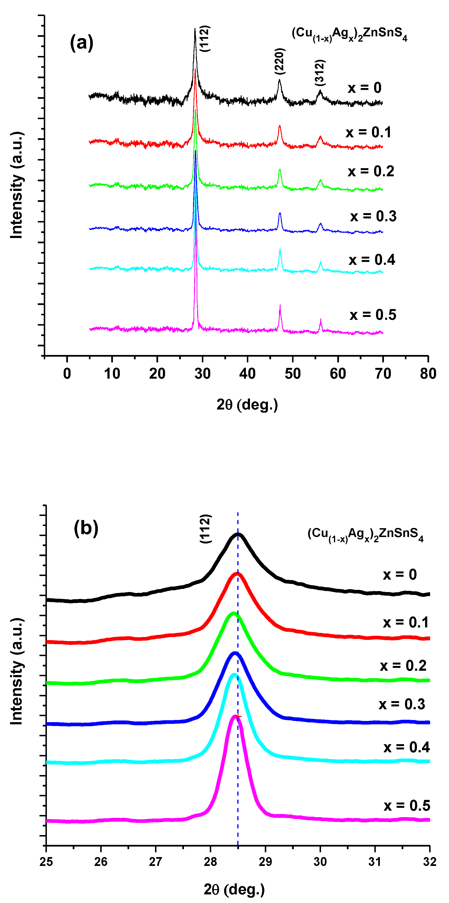
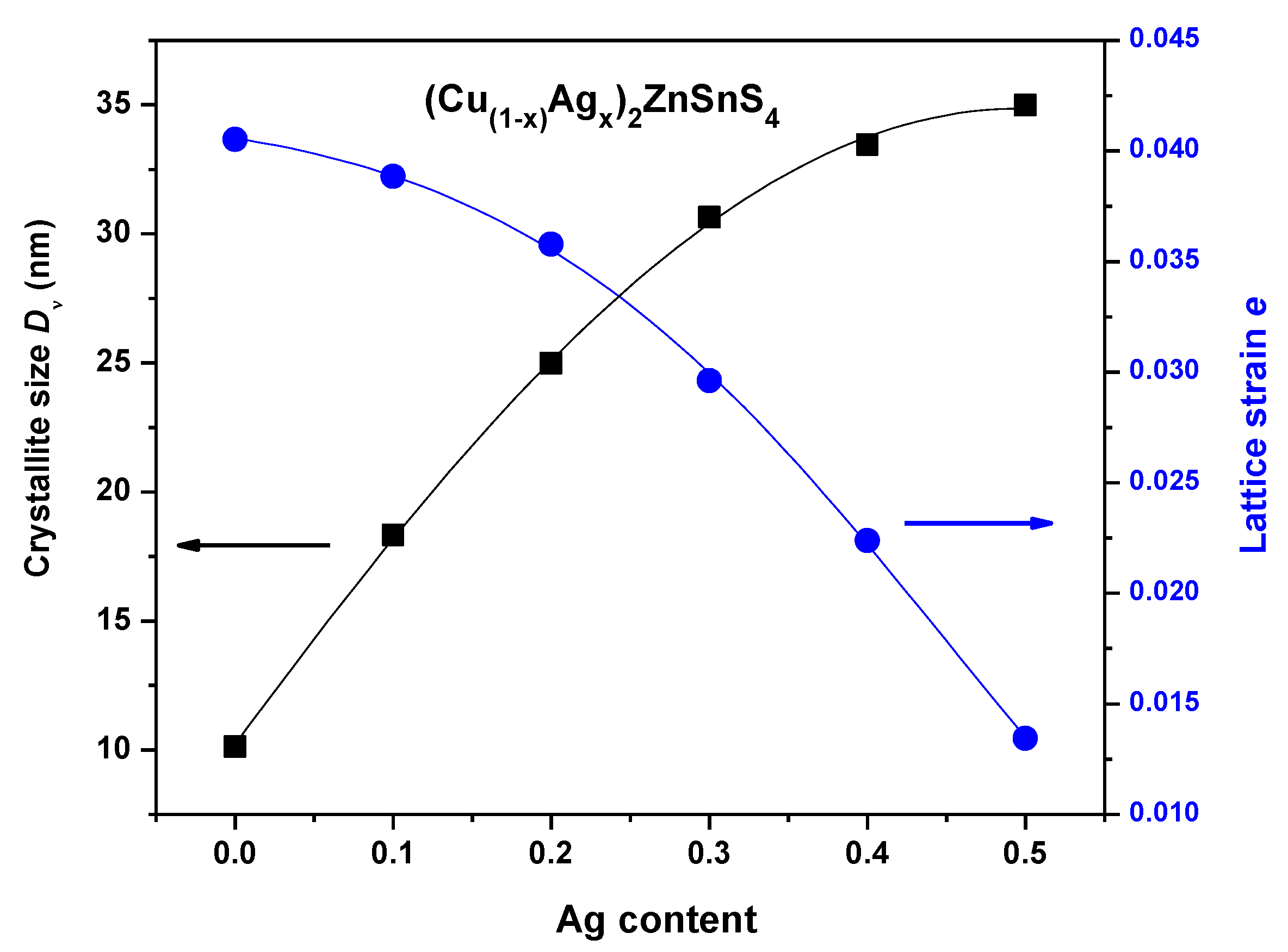
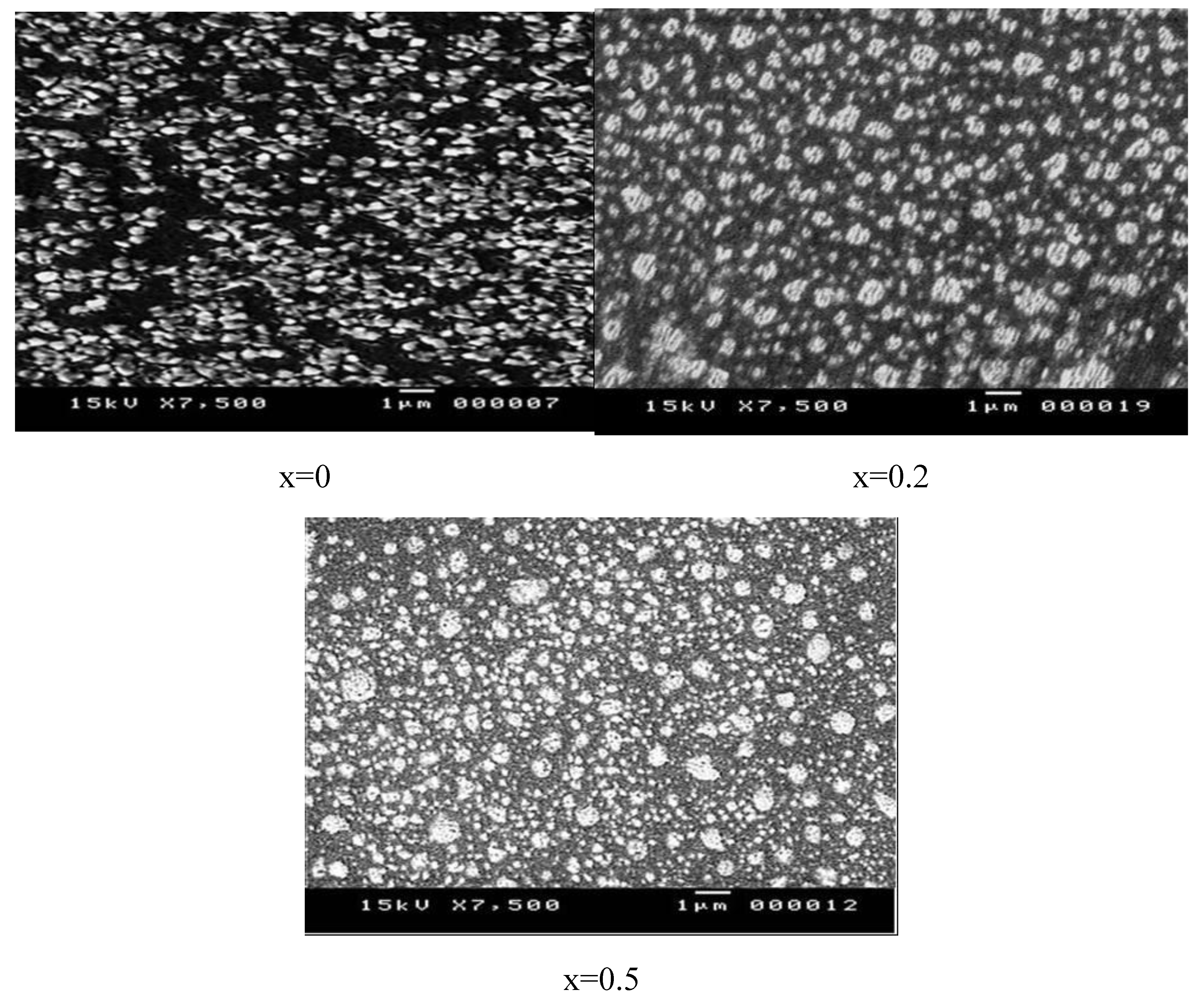
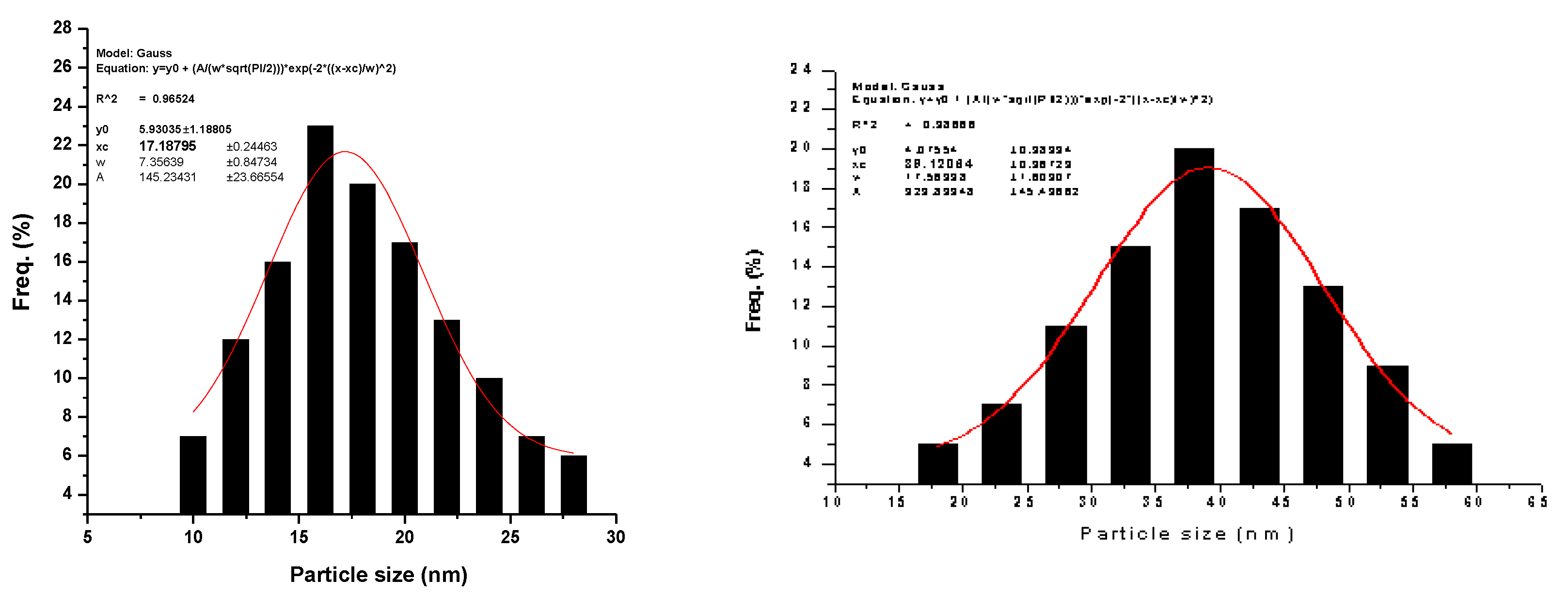
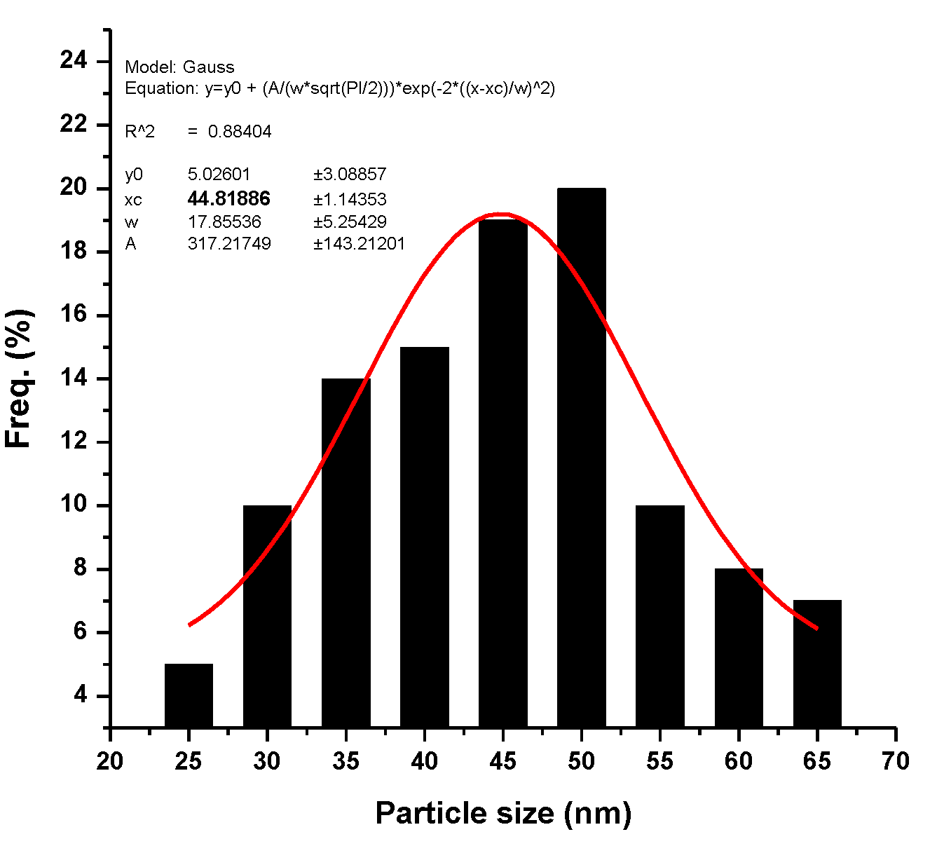
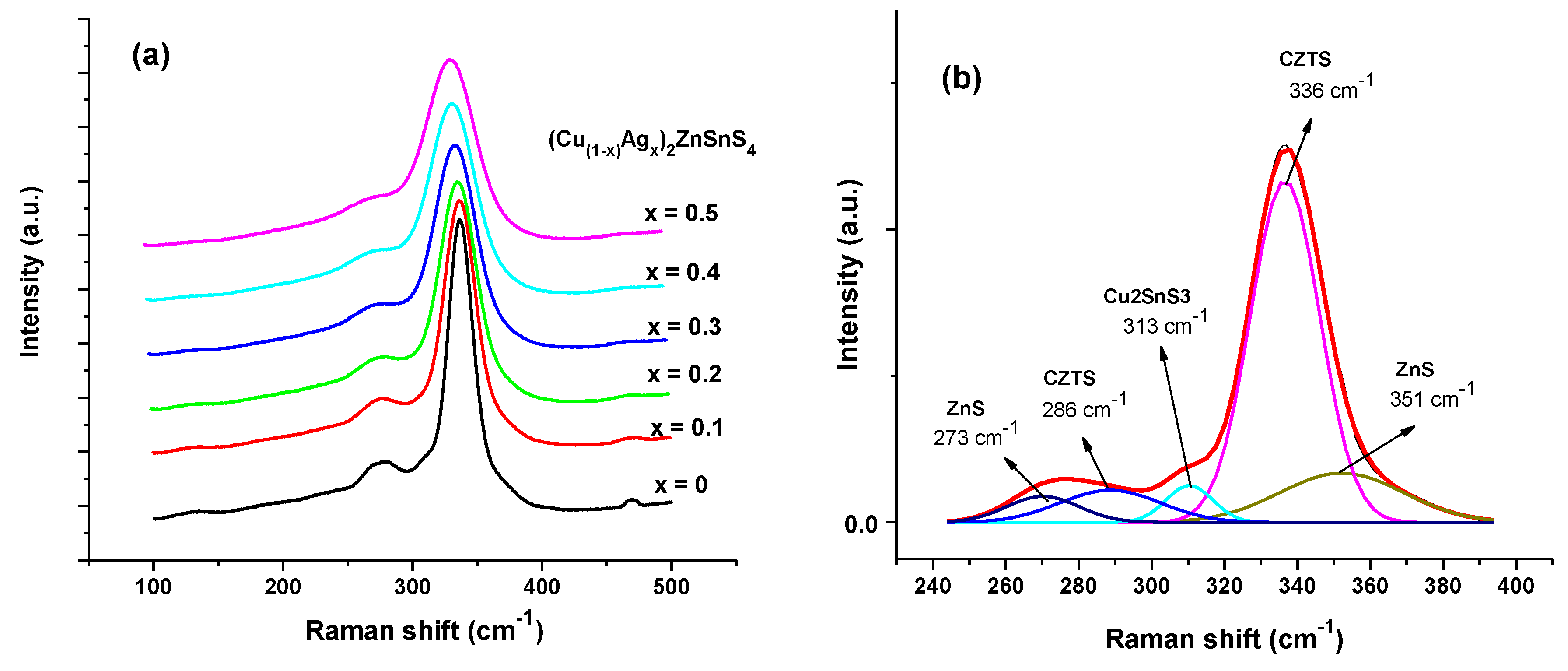
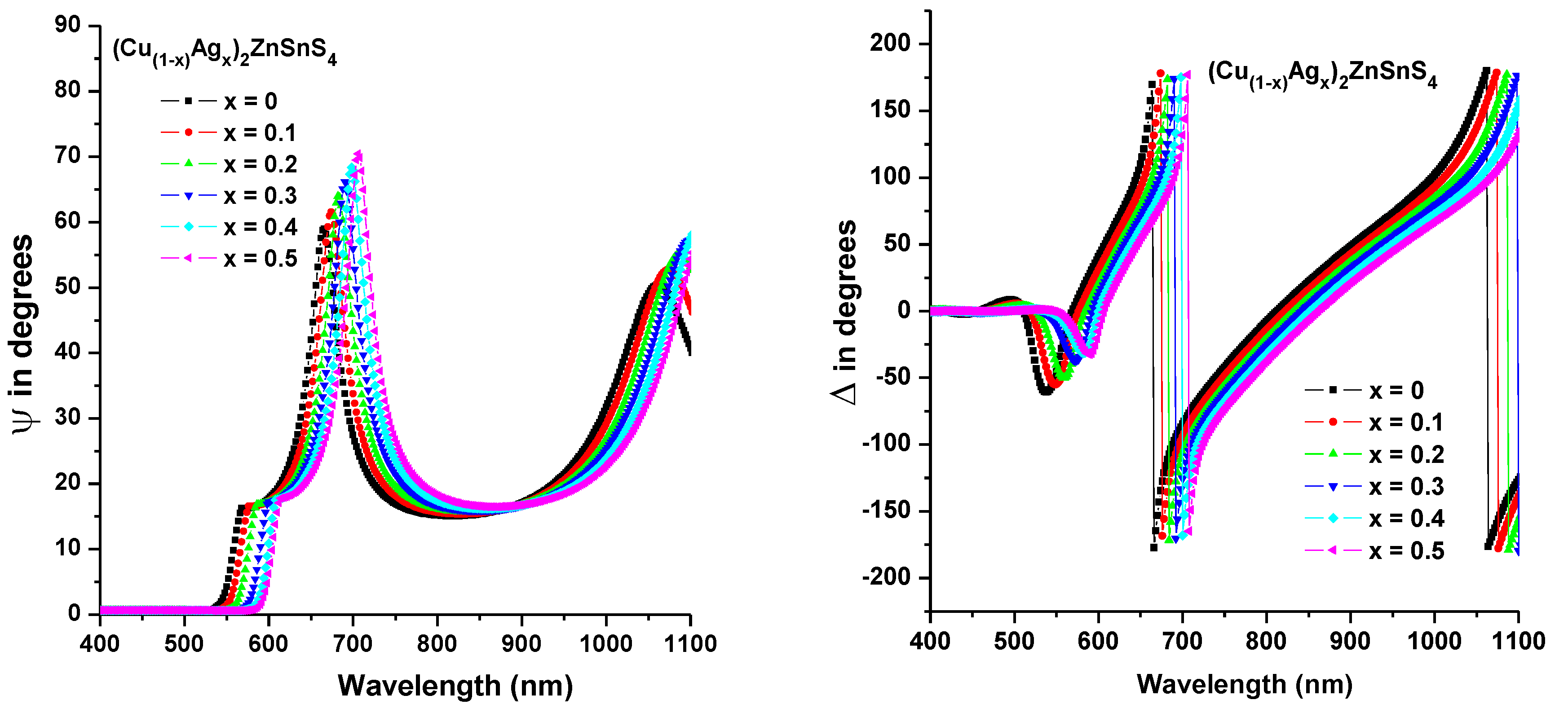
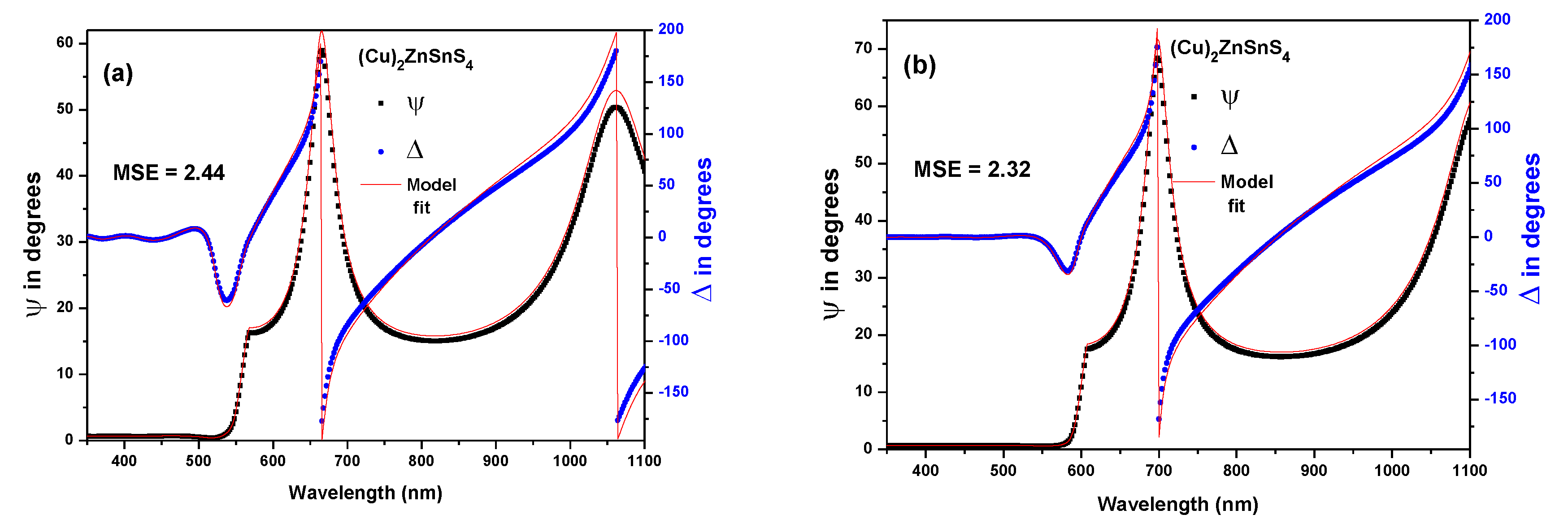

| x | Cu (mV) | Ag (at/%) | Zn (at/%) | Sn (at/%) | S (at/%) |
|---|---|---|---|---|---|
| 0 | 21.06 | 0 | 11.71 | 11.83 | 55.4 |
| 0.1 | 19.11 | 2.03 | 11.81 | 11.94 | 55.11 |
| 0.2 | 17.21 | 4.05 | 11.78 | 11.93 | 55.03 |
| 0.3 | 15.04 | 6.12 | 11.68 | 11.91 | 55.25 |
| 0.4 | 12.88 | 8.52 | 11.82 | 11.87 | 54.91 |
| 0.5 | 10.88 | 10.21 | 11.85 | 11.93 | 55.13 |
Disclaimer/Publisher’s Note: The statements, opinions and data contained in all publications are solely those of the individual author(s) and contributor(s) and not of MDPI and/or the editor(s). MDPI and/or the editor(s) disclaim responsibility for any injury to people or property resulting from any ideas, methods, instructions or products referred to in the content. |
© 2024 by the authors. Licensee MDPI, Basel, Switzerland. This article is an open access article distributed under the terms and conditions of the Creative Commons Attribution (CC BY) license (http://creativecommons.org/licenses/by/4.0/).


