Submitted:
18 June 2024
Posted:
18 June 2024
You are already at the latest version
Abstract
Keywords:
1. Introduction
2. Methods
2.1. Principle of the Proposed Corona Suppression Method
2.2. Description of the Devices Under Test (DUT)
2.3. Measurement System of Microwave Corona Breakdown
3. Results and Discussions


4. Conclusions
Author Contributions
Funding
Data Availability Statement
Conflicts of Interest
References
- M, Yu. Power-handling capability for RF filters. IEEE Microwave Magazine, 2007, 7: 88-97. [CrossRef]
- Abbas Semnani, Kenle Chen, and Dimitrios Peroulis. Microwave gas breakdown in tunable evanescent-mode cavity resonators. IEEE Microwave and Wireless Components Letters, 24(5): 351-353, 2017. [CrossRef]
- Amir Rezagholi., Farzad Mohajeri. Construction, simulation, and experimental verification of a gas-discharge plasma waveguide phase shifter. AEU-International Journal of Electronics and Communications, 2019(08): 195-205. [CrossRef]
- Ulf Jordan, Daria S. Dorozhkina, Vladimir E. Semenov, Torbjrn Olsson, Dan Anderson, Mietek Lisak, Jrme Puech, Igor M. Nefedov, IIya A. Shereshevskii. Microwave corona breakdown around metal corners and wedges. IEEE Transactions on Plasma Science, 2007, 35(3):542-550. [CrossRef]
- T. Pinheiro-Ortega, J. T. Pinheiro-Ortega, J. Monge, S. Marini, J. Sanz, E. Sorolla, M. Mattes, C. Vicente, J. Gil, V. E. Boria, B. Gimeno. Microwave corona breakdown prediction in arbitrarily-shaped waveguide based filter. IEEE Microwave and Wireless Components Letters, 2010, 20(4):214-216. [CrossRef]
- Chen Ze-Yu, Peng Yu-Bin, Wang Rui, He Yong-Ning, Cui Wan-Zhao. Reaction dynamic process of low pressure discharge plasma in microwave resonant cavity. Acta Physica Sinica, 2022, 71(24): 1000-3290. [CrossRef]
- Stefano Sirci, Miguel Ángel Sánchez-Soriano, Jorge D. Martínez, Vicente E. Boria, Fabrizio Gentili, Wolfgang Bösch, Roberto Sorrentino. Design and multiphysics analysis of direct and cross-coupled SIW combline filters using electric and magnetic couplings. IEEE Transactions on Microwave Theory and Techniques, 63(12): 4341-4354, 2015. [CrossRef]
- Miguel, Á. Sánchez-Soriano, Yves Quéré, Vincent Le Saux, Stephan Marini, Marta S. Reglero, Vicente E. Boria, Cédric Quendo. Peak and average power handling capability of microstrip filters. IEEE Transactions on Microwave Theory and Techniques, 67(8): 3436-3448, 2019. [CrossRef]
- G. Feng, Y. G. Feng, Y. Li, X. Li, H. Zhang, and L. Liu. Characteristics of electron evolution during initial low-pressure discharge stage upon microwave circuits. AIP Advances 12, 115129 (2022). [CrossRef]
- F. J. Perez Soler, S. F. J. Perez Soler, S. Anza, M. Mattes, C. M. Espana, F. Quesada, M. Jimenez, J. Gil, C. Vicente, J. R. Mosig, D. Raboso, V. E. Boria, B. Gimeno and A. Alvarez-Melcon. Rigorous investigation of RF breakdown effects in high power microstrip passive circuits. 2009 IEEE MTT-S International Microwave Symposium, 833-836 07- Boston, MA, USA. 12 June. [CrossRef]
- Aitor Morales-Hernández, Miguel Á. Sánchez-Soriano, Stephan Marini, Vicente E. Boria, and Marco Guglielmi. Increasing peak power handling in microstrip bandpass filters by using rounded-end resonators. IEEE Microwave and Wireless Components Letters, 2021, 31(3): 237-240. [CrossRef]
- Aitor Morales-Hernández, Miguel Á. Sánchez-Soriano, Miguel Ferrando-Rocher, Stephan Marini, and Vicente E. Boria. In-depth study of the corona discharge breakdown thresholds in groove gap waveguides and enhancement strategies for inductive bandpass filters. IEEE Access, 2022, 10: 129149-129162. [CrossRef]
- Aitor Morales-Hernández, Miguel Á. Sánchez-Soriano, Stephan Marini, Vicente E. Boria. Marco Guglielmi. Cover-ended resonators to increase corona discharge thresholds in microstrip bandpass filters. Proceedings of the 50th European Microwave Conference, 2020, 882-885. Utrecht, Netherlands. [CrossRef]
- Antonio Romera Perez, Alejandro Pons Abenza, Fernando D. Quesada Pereira, Juan Hinojosa Jimenez, Alejandro Alvarez Melcon, Juan Sebastion Gomez Diaz. A novel low-pass filter based on dielectric impedance inverters to enhance the multipactor breakdown threshold. AEU-International Journal of Electronics and Communications, 2022, (143): 154040. [CrossRef]
- G Feng, H Song, Y Li, X Li, G Xie, J Zhuang and L Liu. Gas desorption and secondary electron emission from graphene coated copper due to E-beam stimulation. Coatings, 2023(13): 370. [CrossRef]
- Morales-Hernández, A. , Sánchez-Soriano, M. Á., Marini, S., Reglero, M. S., Esteve, L., Boria, V. E., and Guglielmi, M. Enhancement of corona discharge thresholds in microstrip bandpass filters by using cover-ended resonators. International Journal of Microwave and Wireless Technologies, 2021, 13(7), 708-718. [CrossRef]
- Nicolas Claus, Kamil Yavuz Kapusuz, Jo Verhaevert and Hendrik Rogier. Compact and Hybrid Dual-Band Bandpass Filter Using Folded Multimode Resonators and Second-Mode Suppression. Electronics, 2024, 13(10): 1921. [CrossRef]
- Pozar D, M. Microwave Engineering, 4th Edition. 2012.John Wiley&Sons, Inc.
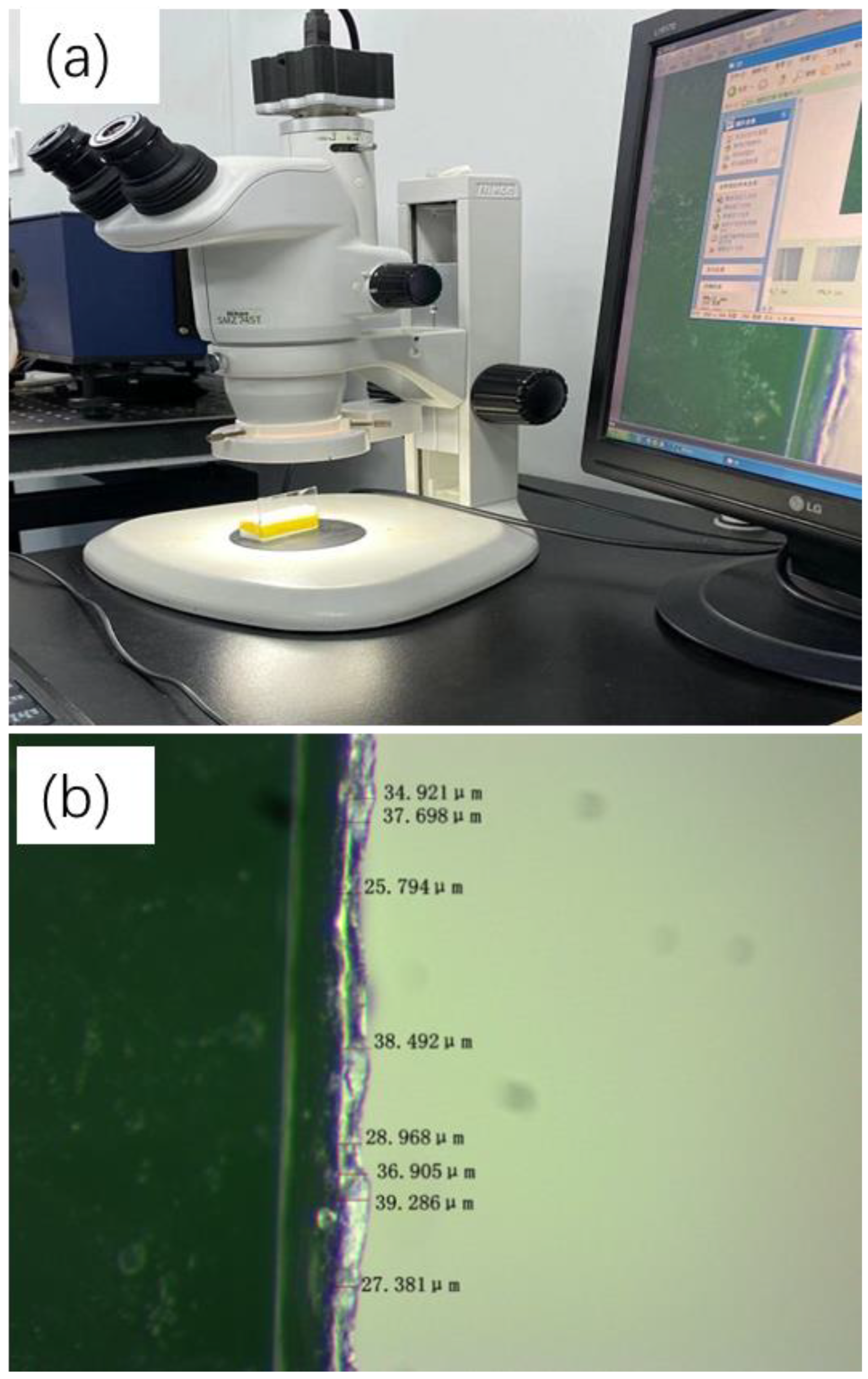
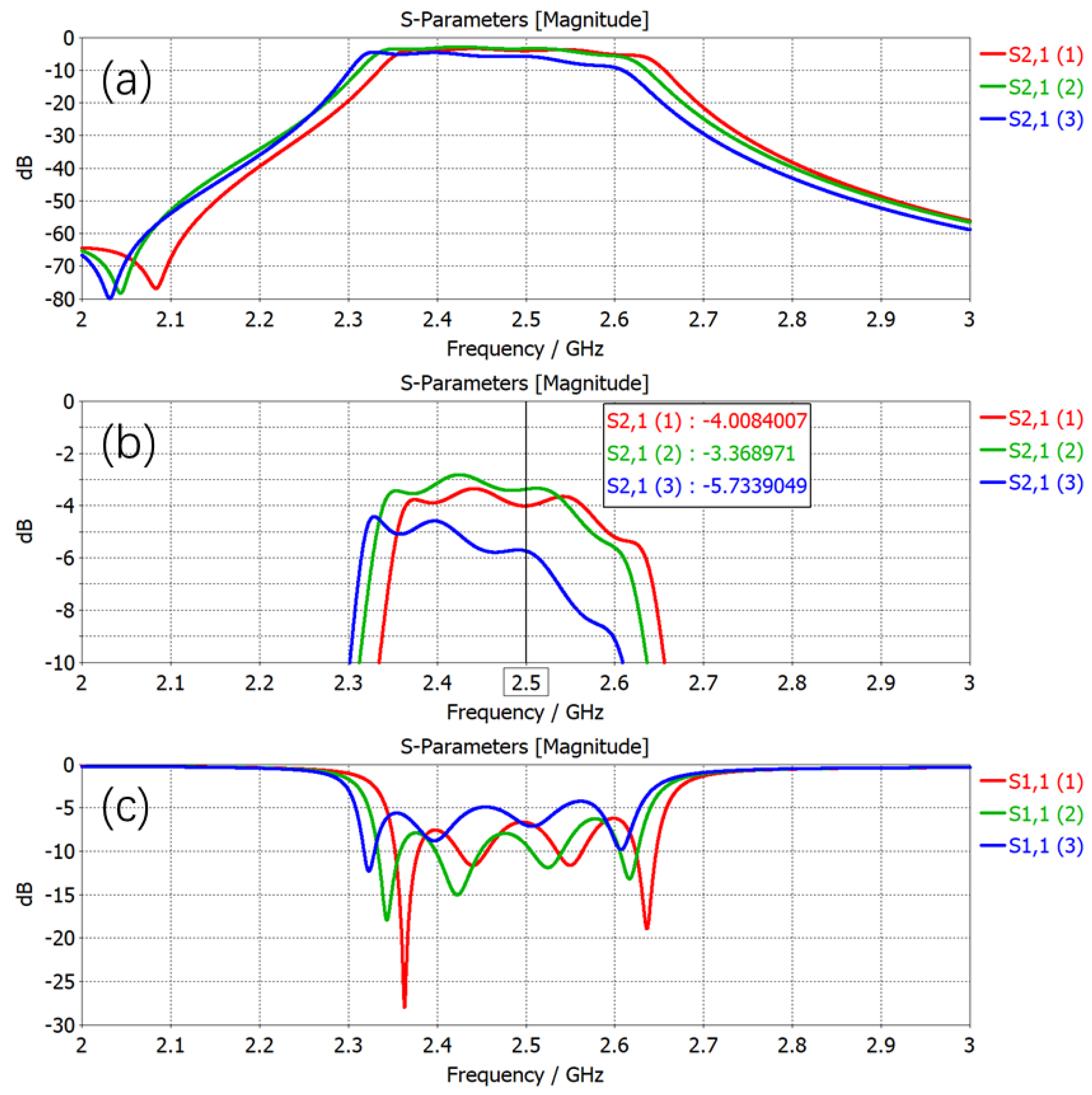
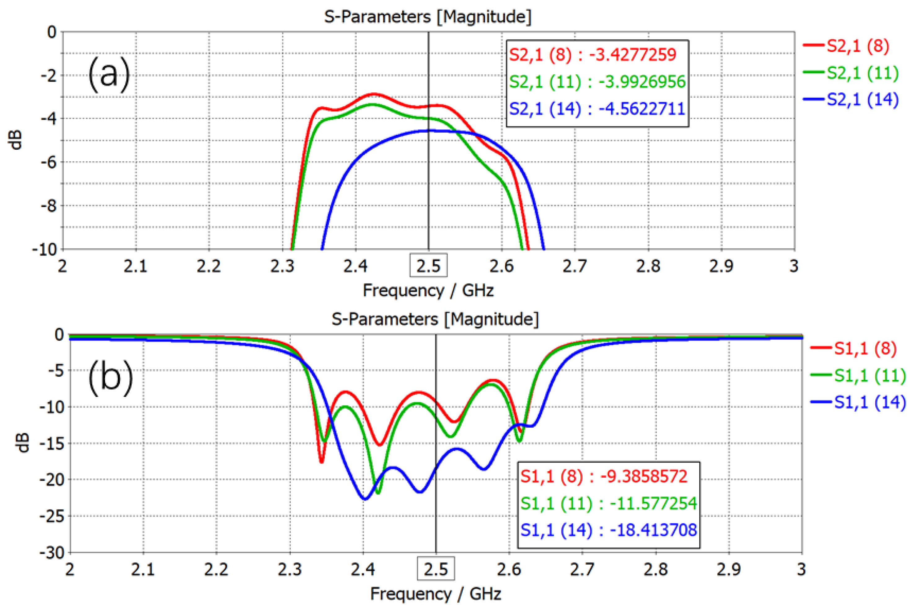

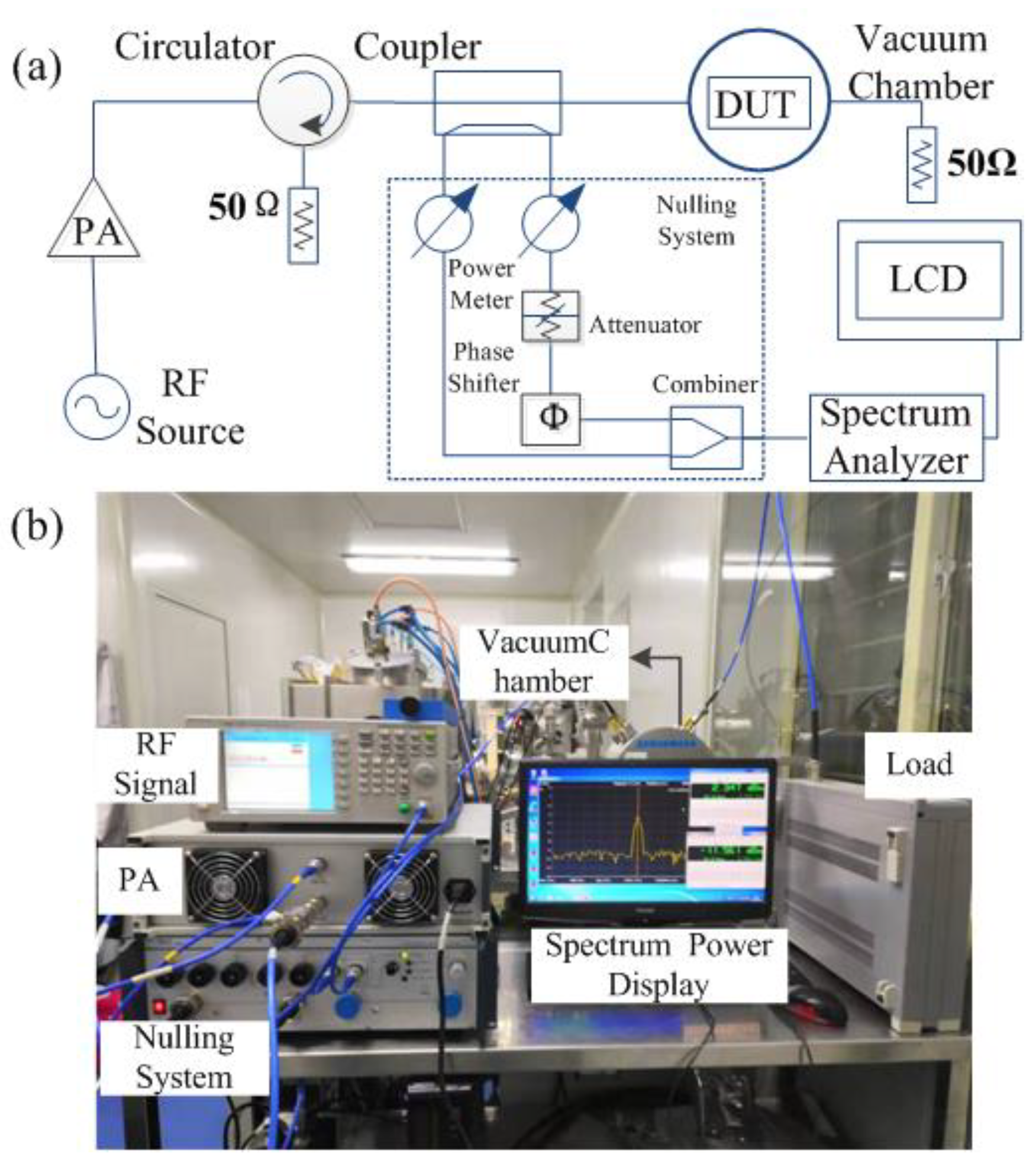
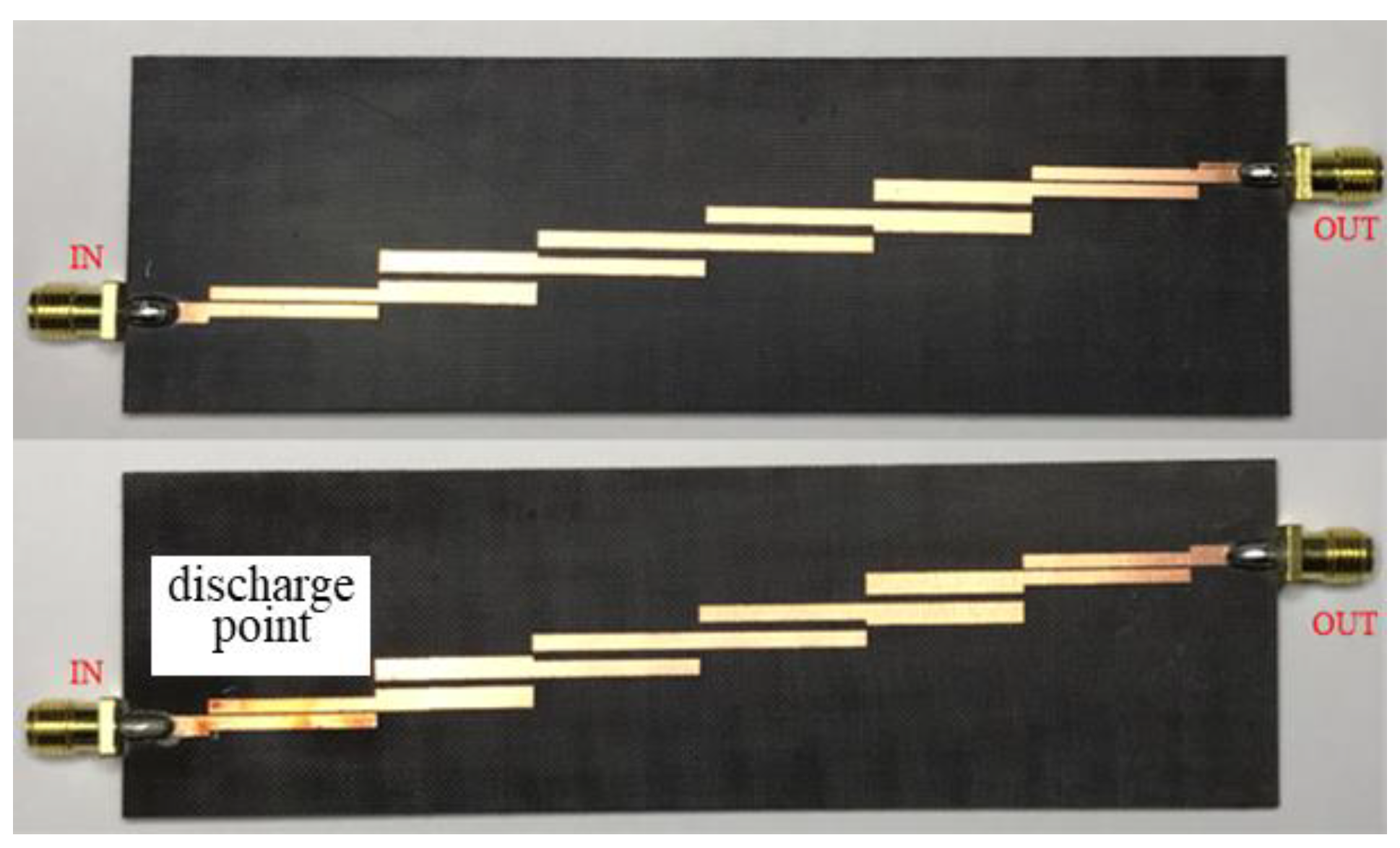
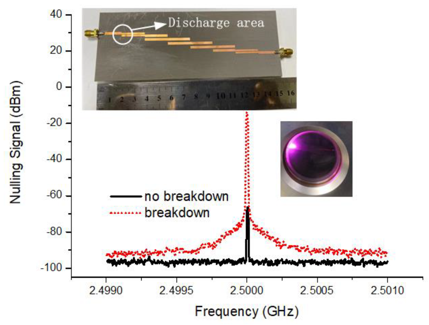
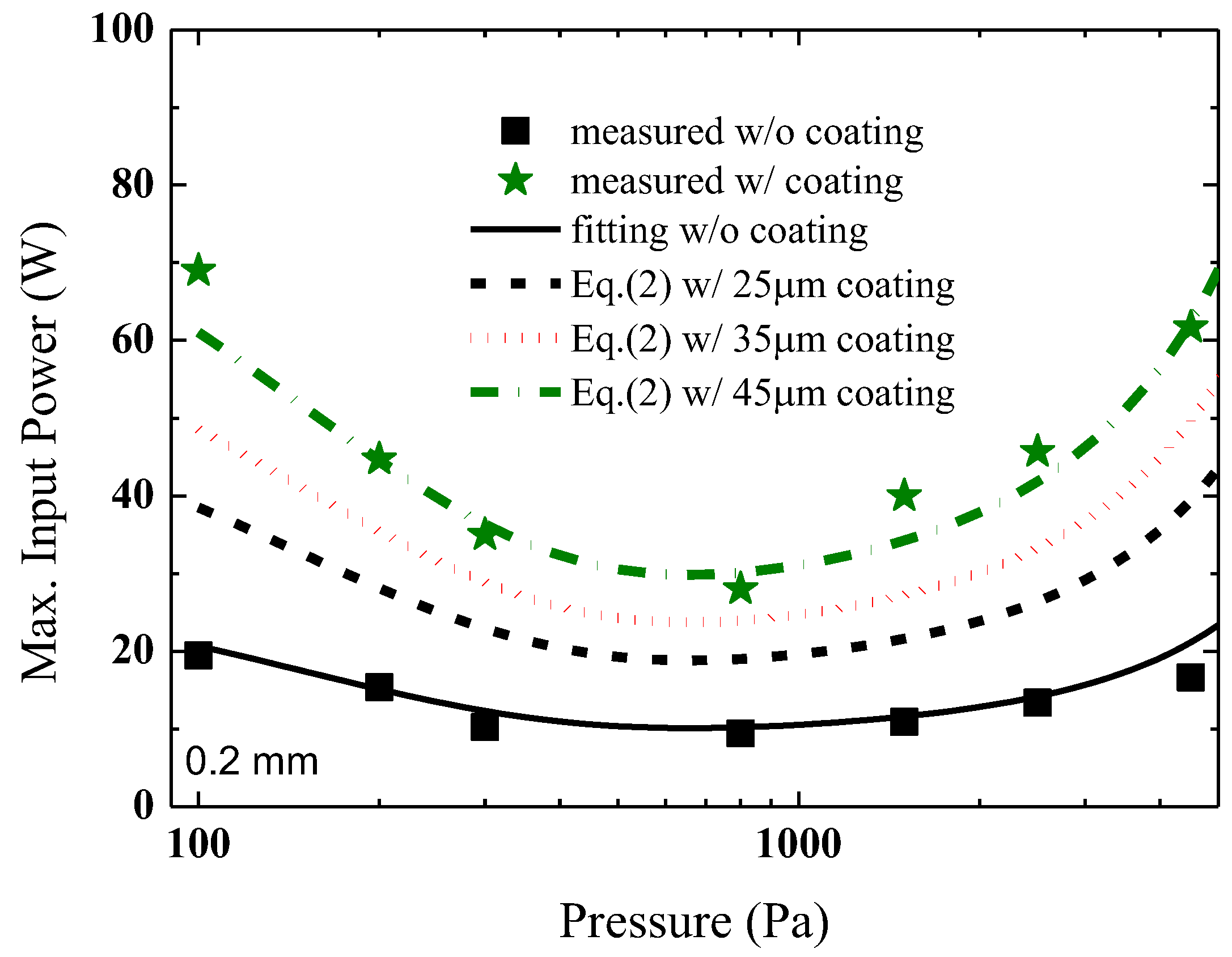
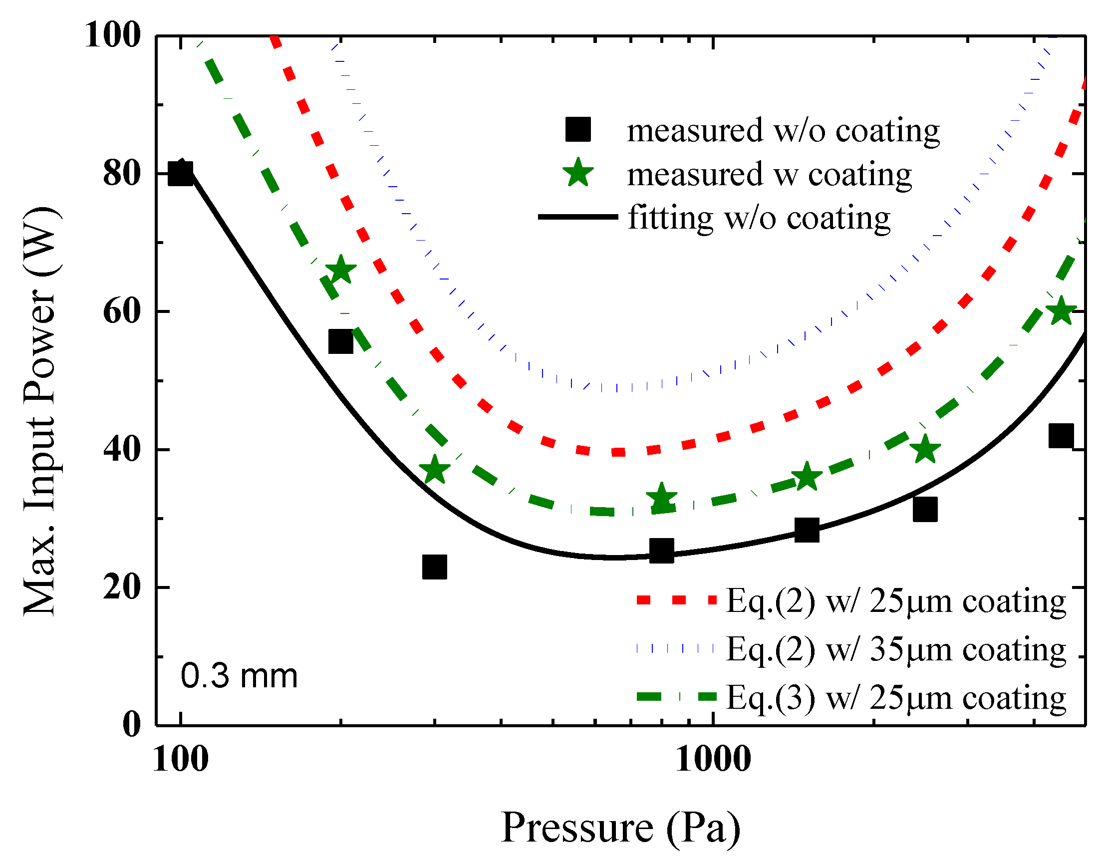
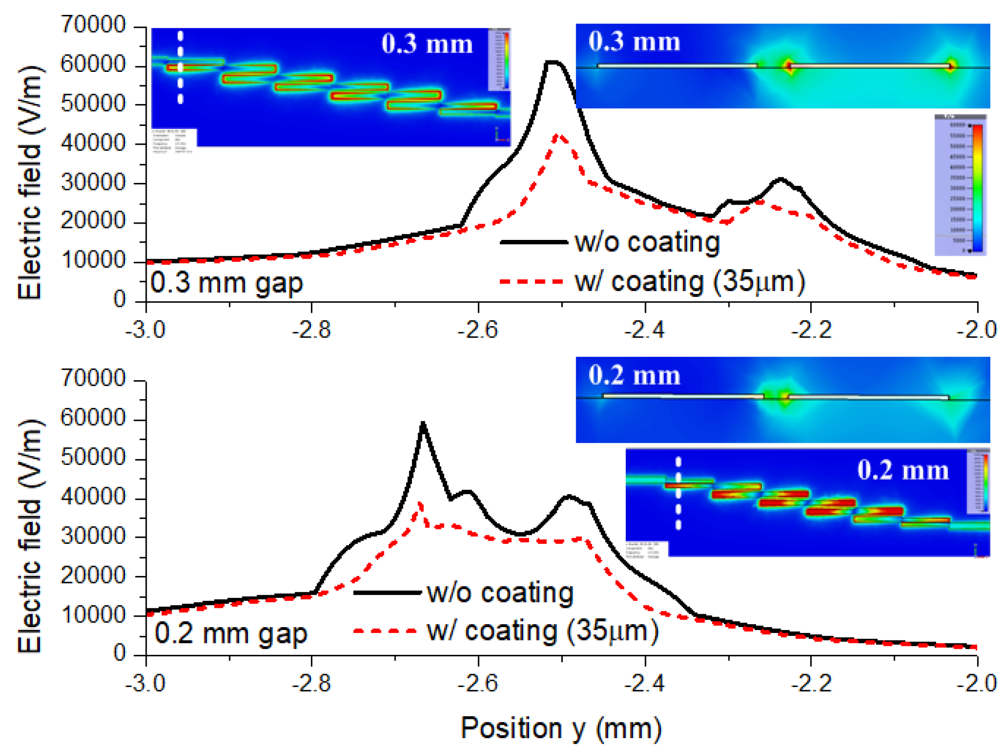
| coating thickness (μm) | 0 | 25 | 35 | 45 |
| corona threshold(W) | 15.8 | 18.9 | 24 | 74.9 |
| Group # | Narrowest gap (mm) | Coating |
|---|---|---|
| 1 | 0.2 | no |
| 2 | 0.3 | no |
| 3 | 0.2 | yes |
| 4 | 0.3 | yes |
| Group # | a1 | a2 | b1 | b2 |
|---|---|---|---|---|
| 1 | 23.0421 | -0.0074 | 8.5909 | 0.0002 |
| 2 | 142.252 | -0.0085 | 20.8847 | 0.0002 |
Disclaimer/Publisher’s Note: The statements, opinions and data contained in all publications are solely those of the individual author(s) and contributor(s) and not of MDPI and/or the editor(s). MDPI and/or the editor(s) disclaim responsibility for any injury to people or property resulting from any ideas, methods, instructions or products referred to in the content. |
© 2024 by the authors. Licensee MDPI, Basel, Switzerland. This article is an open access article distributed under the terms and conditions of the Creative Commons Attribution (CC BY) license (https://creativecommons.org/licenses/by/4.0/).


