1. Introduction
In recent years, with the rapid development of generative artificial intelligence led by ChatGPT, as well as electric vehicles, the constant demand for chips with higher communication capacity has triggered a semiconductor shortage [
1,
2]. Meanwhile, there has also been an explosion in the volume of global data. International Data Corporation predicts that the global datasphere will grow from 33 ZB in 2018 to 175 ZB by 2025 [
3]. Due to limitations in bandwidth, heat, and latency, traditional electrical communication systems face significant challenges with expanding data volumes [
4,
5,
6]. Using optical signals instead of electrical signals to transmit information, ultra-short range optical communication has gained attention due to its high bandwidth capacity, low latency, and high security [
7]. For example, research on inter-chip optical communications in multi-chip packages has been extensively reported [
8,
9,
10]. There are high expectations for photonic crystals (PhCs) to achieve inter-chip optical communications due to their strong light confinement and low propagation loss. A PhC is a nanostructure consisting of a periodic arrangement of materials with different refractive indexes [
11,
12,
13,
14,
15,
16]. This configuration creates a photonic bandgap, and no photon whose energy lies within the bandgap can propagate through the PhC. By setting defects in PhC structures, photons located in the bandgap can be confined within the defects. Changing the position or shape of the defects allows the defects to be used as cavities or waveguides, enabling fine manipulation of light at the nanometer level. Due to this feature, various kinds of PhC lasers have been researched and developed [
17,
18,
19,
20,
21,
22]. However, current-injected lasers are essential for optical interconnects, but there are few reports of current-injected PhC defect lasers. For example, H.G. Pork et al. placed a sub-micrometer-sized InP post at the center of the single-cell PhC resonator for the current injection. However, this post absorbs light in the center of the resonator, and the small cross-sectional area of the post leads to high resistance, so this laser could only operate under a pulse current [
23]. B. Ellis et al. demonstrated a quantum-dot PhC nanocavity laser in GaAs with very low threshold current. However, continuous-wave lasing was observed at 150 K but not at room temperature [
24]. G. Crosnier et al. reported laser diodes based on 1-dimensional PhC nanocavities made in InP nanoribs. Room-temperature continuous-wave (RT-CW) single-mode operation was obtained, but the threshold current of 100 μA was too high for optical interconnects [
25]. The lambda-scale embedded active region photonic-crystal (LEAP) laser developed by Nippon Telegraph and Telephone Corporation (NTT) is a PhC defect laser that allows lateral current injection. It achieved RT-CW lasing and has an ultra-low threshold current of 4.8 μA and an operating energy of 4.4 fJ bit
-1 [
26,
27,
28,
29]. However, LEAP lasers are not available for wavelength division multiplexing (WDM), so they are still far from practical application.
It has been calculated that a communication capacity density of 10 Tbps cm
-2 or 10 Pbps cm
-2 is required to achieve inter-chip or intra-chip optical communications, respectively [
30,
31]. We proposed a circular defect in 2D photonic crystal (CirD) laser that has the potential to reach these values [
31,
32] and allows vertical current injections. We need to develop fabrication technology due to the large thickness of the device for vertical current injection. It is fabricated on a GaAs/AlGaAs heteroepitaxial wafer. The structure consists of a GaAs core layer containing InAs quantum dots (QDs), sandwiched between two AlGaAs cladding layers, and a GaAs contact layer covering the upper cladding layer. The AlGaAs cladding layers are oxidized to AlGaO
x which confines the light to the core layer [
33]. The center of the CirD cavity remains unoxidized to form an AlGaAs funnel that allows a current injection into the cavity. The whispering gallery mode (WGM) is generated by injecting power into the cavity. If the frequencies of the WGM match the frequencies of the waveguide mode, the light enters the waveguide and propagates through it, eventually exiting the waveguide’s end face. The lasing wavelength can be changed by adjusting the cavity radius, so wavelength division multiplexing can be achieved easily by coupling multiple CirD cavities, each with a different lasing wavelength, to a single output waveguide. We previously proposed an orthogonal lattice waveguide (OLW) and demonstrated both theoretically and experimentally that it has a bandwidth of 20 nm and can support 20-channel WDM with a bandwidth interval of 1 nm [
34,
35]. The size of a CirD laser array containing 20 cavities can be limited to 10
-4 cm
2 [
31], so it is possible to achieve optical communications within the chip due to its ultra-small size.
As mentioned above, light is output from the end face of the waveguide. In sample fabrication, the output end face is usually formed by cleaving the sample along the direction perpendicular to the waveguide. However, since the cleavage position has an error of at least 10 μm, the actual cleavage position affects the output optical power for a nanoscale sample. We proposed a convex edge structure in a previous study and performed simulations. The optical output can be improved by setting semicircular ports on the output end face and changing the waveguide near the port to a line defect (W1) waveguide (see Figure 4 in [
36]). In this paper, we develop fabrication techniques for CirD lasers with convex edge structures that eliminate the effects caused by the cleavage position. We also fabricate samples and measure their optical characteristics by photoexcitation.
2. Structure and Fabrication
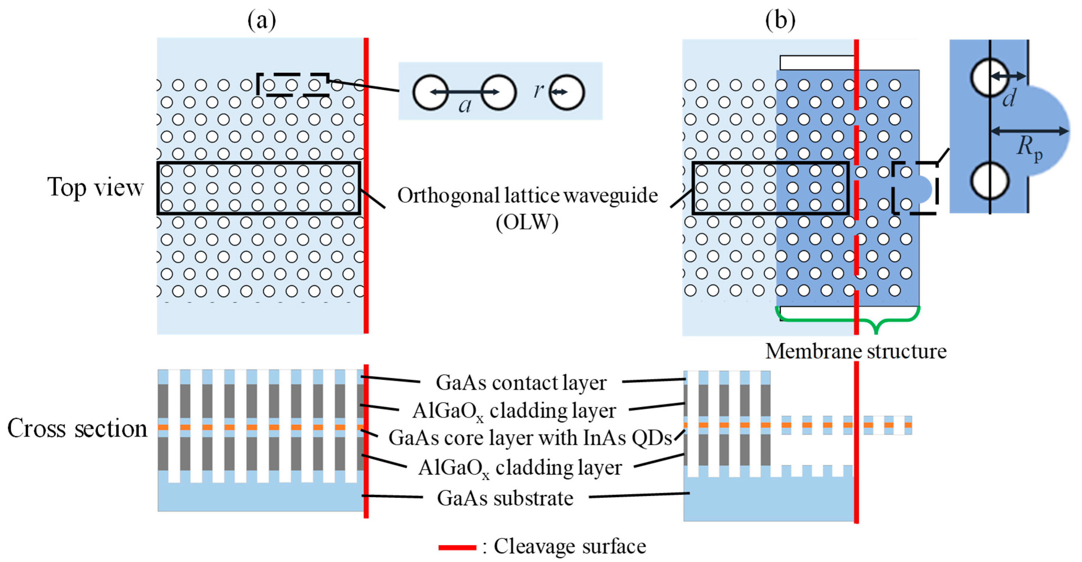
The schematics of the edge structure produced by conventional cleavage and the convex edge structure are shown in
Figure 1a,b, respectively. In the convex edge structure, only the GaAs core layer is retained near the output end face and floats in the air, which we refer to as the membrane structure. As can be seen from the top view, the membrane structure is connected to the wafer only on the left side, while a very deep trench is at the other three sides. As long as the cleaving position is within the trench, the membrane structure will not be damaged after cleavage. In addition, the cavity retains upper and lower cladding layers that still allow current injection.
The process flow diagram is shown in
Figure 2. The thicknesses of the GaAs contact layer, upper AlGaAs cladding layer, GaAs core layer containing three InAs QD layers, and lower AlGaAs cladding layer are 180, 550, 220, and 550 nm, respectively. The photoluminescence peak of the QDs is 1289 nm. Steps 1 and 2: We drew PhC and edge structure patterns on the wafer by electron beam (EB) lithography and etched the patterns by dry etching. Here, the lattice constant of triangular lattice
a and the airhole radius
r are 365 and 115 nm, respectively. The edge face position
d is 165 nm, which is the distance from the edge face to the center of the airhole row closest to the edge face. The radius of the semicircular port
Rp is 420 nm. The radius of CirD laser cavity
R is 2.78
a. The values of these parameters were adopted from the optimal values previously obtained by calculation [
36]. Step 3: We oxidized AlGaAs to AlGaO
x in H
2O/N
2 steam at 395°C for 45 minutes. At this point, the AlGaAs at the cavity would be completely oxidized to AlGaO
x and current injection would be impossible. This is because ultimately only optical measurements would be performed, and complete oxidation can enhance light confinement. Steps 4 and 5: We performed an overlaid EB lithography and another dry etching to remove the contact layer of the membrane structure. Step 6: We removed the AlGaAs/AlGaO
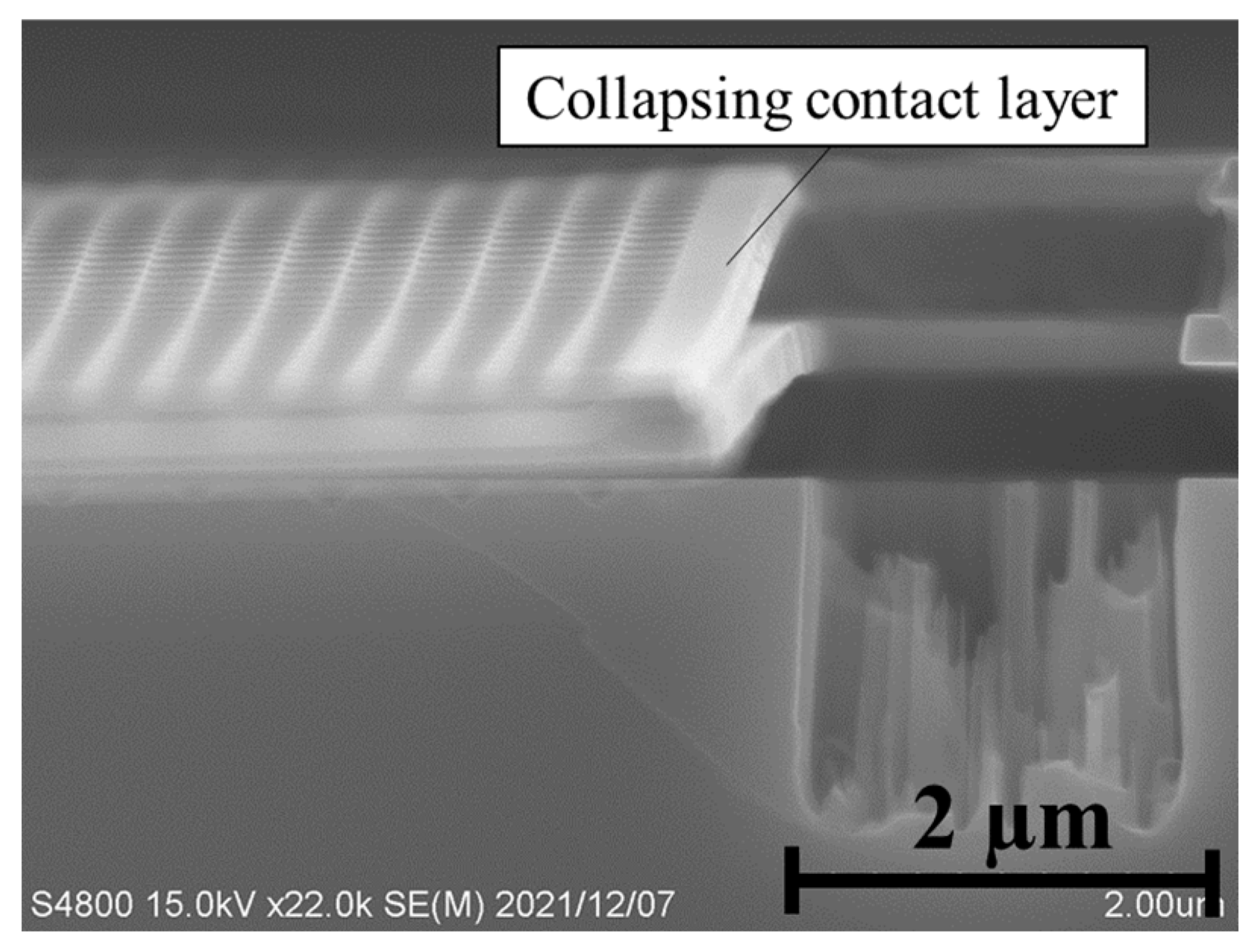
x cladding layers of the membrane structure by BHF wet etching. Steps 4 and 5 were not taken in the initial fabrication process. But even without these two steps, the membrane structure of the fabricated sample at this point would float in the air, and only the contact layer that was not removed by wet etching would remain above it. However, after fabricating some samples, we noticed that the contact layers collapsed due to their weight.
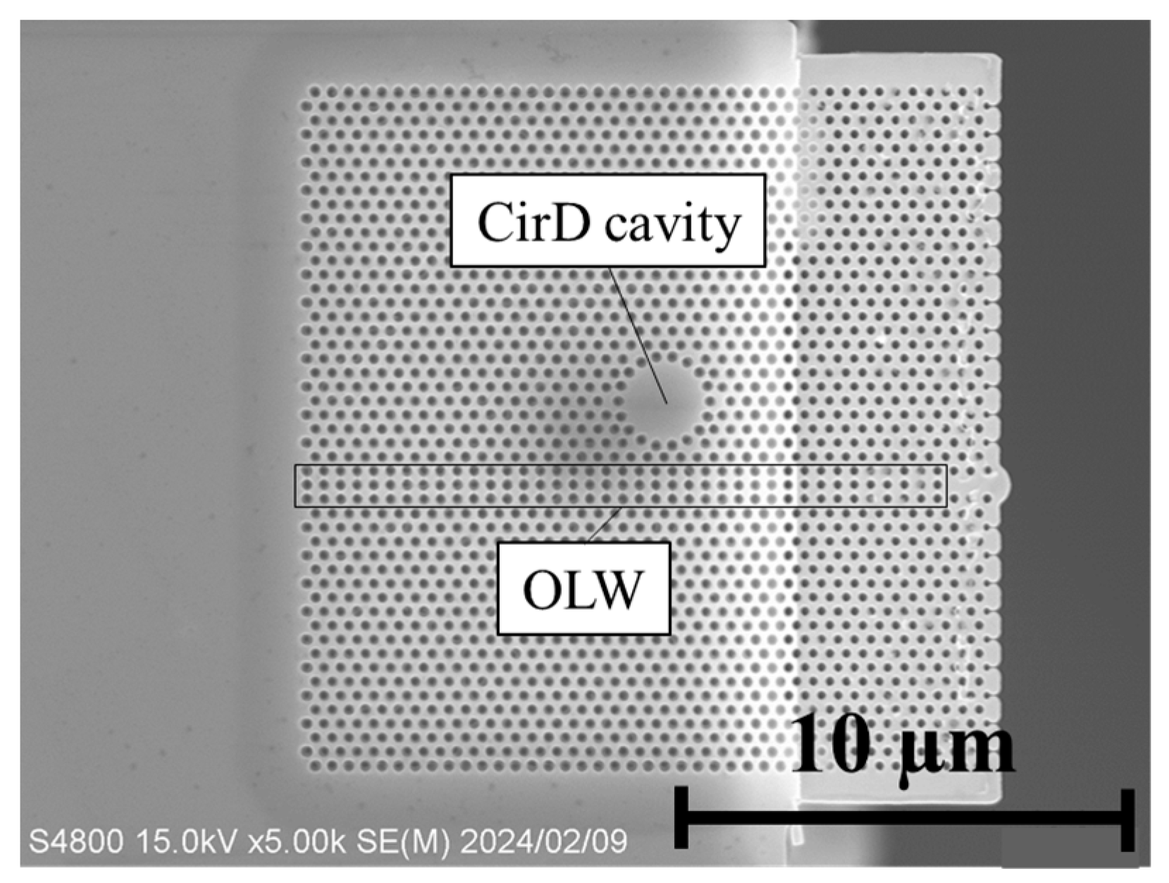
Figure 3 shows the cross-sectional SEM image of a sample with a collapsing contact layer. Therefore, we added steps 4 and 5 to remove the contact layer of the membrane structure. Step 7: We cleaved the sample. The top-view SEM image of the sample after cleavage is shown in
Figure 4. Finally, the sample was fabricated successfully as designed.
3. Optical Measurement and Results
We used an AlGaAs semiconductor laser with a wavelength of 785 nm as the pump light source. The laser beam was focused on the surface of the CirD cavity using a microscope’s objective lens, resulting in a spot size of 2 μm. The convex edge emitted light collected with a lensed fiber that was split into two paths. One path directed the light to a photodiode (PD) array (ANDOR, iDus InGaAs 1.7 µm) via a monochromator (LUCIR, Z-3008). The other path directed the light to an optical spectrum analyzer (OSA: Yokogawa, AQ6370D).
The PD array was used for quick measurements of the spectra to determine the threshold powers. The OSA was employed to measure the spectra with higher precision and determine the full width at half maximum (FWHM). The monochromator and the OSA had resolutions of approximately 0.4 and 0.02 nm, respectively. These instruments allowed for accurate spectral analysis in the experiments.
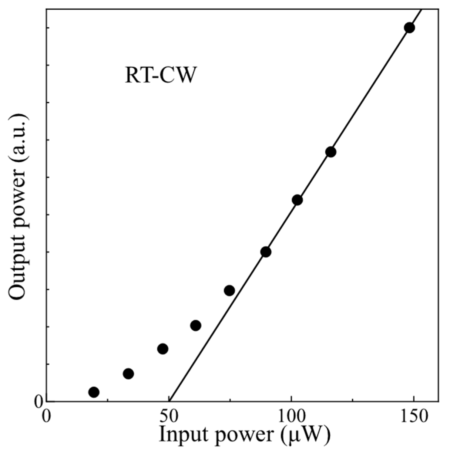
Figure 5 shows the relationship between output power and input power for the sample measured by the PD array and monochromator. The lasing threshold power (
Pth) can be obtained as
Pth = 50 μW. This value is close to the threshold power for the well-lasing sample obtained in our previous study [
37].
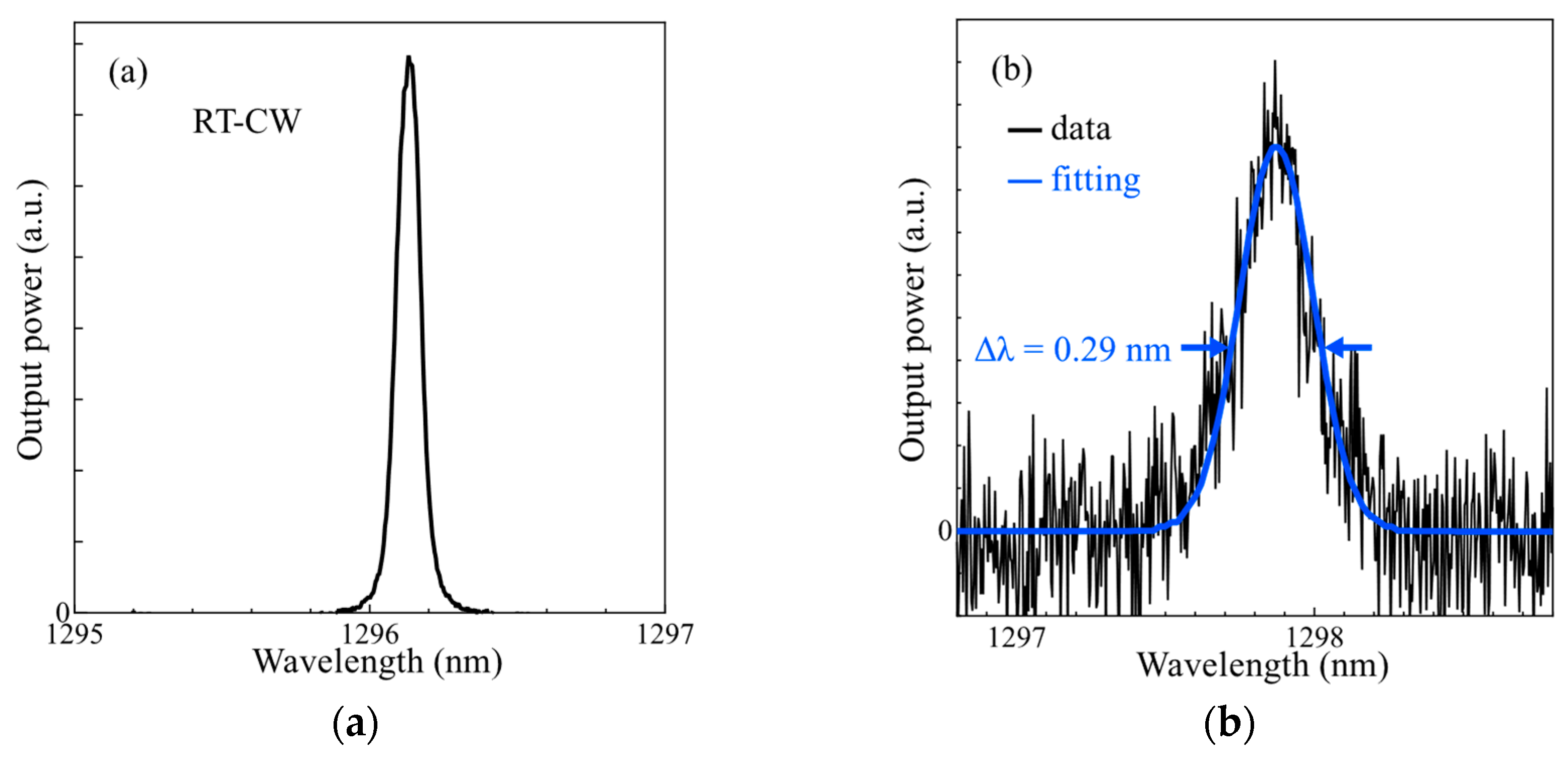
Figure 6a shows the spectrum of this sample measured by the OSA, and the input power was set to 210 μW. A spectrum with a wavelength span = 60 nm at the same input power was also measured, and single mode lasing due to WGM was observed in the 1.3 μm range.
Figure 6b shows the spectrum measured at the input power of 48 μW, which is close to the threshold power. Its FWHM or
Δλ was estimated to be 0.29 nm by fitting it to a Gaussian function. The quality factor (
Q) of a CirD cavity can be calculated as 4433 using the formula of
Q =
λ/
Δλ. Since the convex edge structure hardly changes the
Q of the CirD laser, it is essentially the same
Q as the well-fabricated samples obtained by the conventional cleaving method, which is consistent with the simulation results of the conventional structure [
38]. The optimum
Q of PhC defect lasers for optical interconnects is 3000-4000. A previous study has shown that too high
Q negatively impacts high-speed operation [
39]. These results indicate that CirD lasers with convex edge structures have similar optical properties to the CirD lasers with RT-CW lasing in previous studies, and RT-CW lasing of a CirD laser with a convex edge structure was achieved for the first time.
4. Conclusions
To eliminate the effect of cleavage position on the optical properties of a CirD laser, we developed fabrication techniques for CirD lasers with convex edge structures. By performing an overlaid EB lithography and dry etching to remove the contact layer of the membrane structure, we prevented the collapse of the contact layer and thus fabricated samples successfully. We measured the optical characteristics of samples by photoexcitation. The RT-CW lasing of the WGM was observed, and it has almost the same optical characteristics as the well-fabricated samples reported in previous studies.
Author Contributions
Conceptualization, R.Z., Y.A., and M.K.; methodology, M.M. and A.M.; validation, R.Z., Y.A., Y.K., and H.Y.; formal analysis, R.Z. and Y.A.; investigation, R.Z., Y.A., Y.K., and H.Y.; resources, T.Y., M.M., H.K. A.M., and M.K.; software, Y.A. and M.M.; data curation, R.Z.; writing—original draft preparation, R.Z. and Y.A.; writing—review and editing, T.Y., M.M., H.K. A.M., and M.K.; visualization, R.Z. and Y.A.; supervision, T.Y., M.M., H.K. A.M., and M.K.; project administration, R.Z. and Y.A.; funding acquisition, M.M., H.K., A.M., and M.K. All authors have read and agreed to the published version of the manuscript.
Funding
This work was partially supported by JSPS KAKENHI Grant Number JP23H01467, ULVAC Inc., and “Nanotechnology Platform Project (Nanotechnology Open Facilities in Osaka University)” of the Ministry of Education, Culture, Sports, Science and Technology, Japan (MEXT) [Grant No.: JPMXP1224OS1016].
Conflicts of Interest
The authors declare no conflicts of interest.
References
- Voas, J.; Kshetri, N.; DeFranco, J.F. Scarcity and global insecurity: The semiconductor shortage. IT Professional 2021, 23, 78–82. [Google Scholar] [CrossRef]
- Frieske, B.; Stieler, S. The “semiconductor crisis” as a result of the COVID-19 pandemic and impacts on the automotive industry and its supply chains. World Electr. Veh. J. 2022, 13, 189. [Google Scholar] [CrossRef]
- Reinsel, D.; Gantz, J.; Rydning, J. The digitization of the world from edge to core. Framingham: International Data Corporation 2018, 16, 1–28. [Google Scholar]
- Neutens, P.; Van Dorpe, P.; De Vlaminck, I.; Lagae, L.; Borghs, G. Electrical detection of confined gap plasmons in metal–insulator–metal waveguides. Nature Photonics 2009, 3, 283–286. [Google Scholar] [CrossRef]
- Conway, J.A.; Sahni, S.; Szkopek, T. Plasmonic interconnects versus conventional interconnects: a comparison of latency, crosstalk and energy costs. Opt. Express 2007, 15, 4474–4484. [Google Scholar] [CrossRef]
- Zia, R.; Schuller, J.A.; Chandran, A.; Brongersma, M.L. Plasmonics: the next chip-scale technology. Materials Today 2006, 9, 20–27. [Google Scholar] [CrossRef]
- Chen, G.; Chen, H.; Haurylau, M.; Nelson, N.; Fauchet, P.M.; Friedman, E.G.; Albonesi, D. Predictions of CMOS compatible on-chip optical interconnect. SLIP ‘05 2005, 13–20. [Google Scholar] [CrossRef]
- Feldman, M.R.; Esener, S.C.; Guest, C.C.; Lee, S.H. Comparison between optical and electrical interconnects based on power and speed considerations. Appl. Opt. 1988, 27, 1742–1751. [Google Scholar] [CrossRef] [PubMed]
- Kachris, C.; Tomkos, I. A survey on optical interconnects for data centers. IEEE Communications Surveys & Tutorials 2012, 14, 1021–1036. [Google Scholar] [CrossRef]
- Taubenblatt, M.A. Optical interconnects for high-performance computing. Journal of Lightwave Technology 2011, 30, 448–457. [Google Scholar] [CrossRef]
- Yablonovitch, E. Inhibited spontaneous emission in solid-state physics and electronics. Phys. Rev. Lett. 1987, 58, 2059. [Google Scholar] [CrossRef] [PubMed]
- Joannopoulos, J.D.; Villeneuve, P.R.; Fan, S. Photonic crystals: putting a new twist on light. Nature 1997, 386, 143–149. [Google Scholar] [CrossRef]
- Akahane, Y.; Asano, T.; Song, B.S.; Noda, S. High-Q photonic nanocavity in a two-dimensional photonic crystal. Nature 2003, 425, 944–947. [Google Scholar] [CrossRef] [PubMed]
- Noda, S.; Tomoda, K.; Yamamoto, N.; Chutinan, A. Full three-dimensional photonic bandgap crystals at near-infrared wavelengths. Science 2000, 289, 604–606. [Google Scholar] [CrossRef] [PubMed]
- Wu, F.; Chen, M.; Xiao, S. Wide-angle polarization selectivity based on anomalous defect mode in photonic crystal containing hyperbolic metamaterials. Opt. Lett. 2022, 47, 2153–2156. [Google Scholar] [CrossRef] [PubMed]
- Wu, F.; Liu, T.; Xiao, S. Polarization-sensitive photonic bandgaps in hybrid one-dimensional photonic crystals composed of all-dielectric elliptical metamaterials and isotropic dielectrics. Appl. Opt. 2023, 62, 706–713. [Google Scholar] [CrossRef] [PubMed]
- Altug, H.; Englund, D.; Vučković, J. Ultrafast photonic crystal nanocavity laser. Nature Phys 2006, 2, 484–488. [Google Scholar] [CrossRef]
- Lončar, M.; Scherer, A.; Qiu, Y. Photonic crystal laser sources for chemical detection. Appl. Phys. Lett. 2003, 82, 4648–4650. [Google Scholar] [CrossRef]
- Noda, S.; Yokoyama, M.; Imada, M.; Chutinan, A.; Mochizuki, M. Polarization mode control of two-dimensional photonic crystal laser by unit cell structure design. Science 2001, 293, 1123–1125. [Google Scholar] [CrossRef]
- Schulz, S.A.; Upham, J.; O’Faolain, L.; Boyd, R.W. Photonic crystal slow light waveguides in a kagome lattice. Opt. Lett. 2017, 42, 3243–3246. [Google Scholar] [CrossRef]
- Ebrahimi, A.; Noori, M. Ultra-slow light with high NDBP achieved in a modified W1 photonic crystal waveguide with coupled cavities. Opt. Commun. 2018, 424, 37–43. [Google Scholar] [CrossRef]
- Matsubara, H.; Yoshimoto, S.; Saito, H.; Jianglin, Y.; Tanaka, Y.; Noda, S. GaN photonic-crystal surface-emitting laser at blue-violet wavelengths. Science 2008, 319, 445–447. [Google Scholar] [CrossRef] [PubMed]
- Park, H.G.; Kim, S.H.; Kwon, S.H.; Ju, Y.G.; Yang, J.K.; Baek, J.H.; Kim, S.B.; Lee, Y.H. Electrically driven single-cell photonic crystal laser. Science 2004, 305, 1444–1447. [Google Scholar] [CrossRef]
- Ellis, B.; Mayer, M.A.; Shambat, G.; Sarmiento, T.; Harris, J.; Haller, E.E.; Vučković, J. Ultralow-threshold electrically pumped quantum-dot photonic-crystal nanocavity laser. Nature Photon 2011, 5, 297–300. [Google Scholar] [CrossRef]
- Crosnier, G.; Sanchez, D.; Bouchoule, S.; Monnier, P.; Beaudoin, G.; Sagnes, I.; Raj, R.; Raineri, F. Hybrid indium phosphide-on-silicon nanolaser diode. Nature Photon 2017, 11, 297–300. [Google Scholar] [CrossRef]
- Matsuo, S.; Shinya, A.; Kakitsuka, T.; Nozaki, K.; Segawa, T.; Sato, T.; Kawaguchi, Y.; Notomi, M. High-speed ultracompact buried heterostructure photonic-crystal laser with 13 fJ of energy consumed per bit transmitted. Nature Photon 2010, 4, 648–654. [Google Scholar] [CrossRef]
- Takeda, K.; Sato, T.; Shinya, A.; Nozaki, K.; Kobayashi, W.; Taniyama, H.; Notomi, M.; Hasebe, K.; Kakitsuka, T.; Matsuo, S. Few-fJ/bit data transmissions using directly modulated lambda-scale embedded active region photonic-crystal lasers. Nature Photon 2013, 7, 569–575. [Google Scholar] [CrossRef]
- Kuramochi, E.; Nozaki, K.; Shinya, A.; Takeda, K.; Sato, T.; Matsuo, S.; Taniyama, H.; Sumikura, H.; Notomi, M. Large-scale integration of wavelength-addressable all-optical memories on a photonic crystal chip. Nature Photon 2014, 8, 474–481. [Google Scholar] [CrossRef]
- Matsuo, S.; Takeda, K. λ-scale embedded active region photonic crystal (LEAP) lasers for optical interconnects. Photonics 2019, 6, 82. [Google Scholar] [CrossRef]
- Arakawa, Y.; Nakamura, T.; Urino, Y.; Fujita, T. Silicon photonics for next generation system integration platform. IEEE Communications Magazine 2013, 51, 72–77. [Google Scholar] [CrossRef]
- Xiong, Y.; Ye, H.; Umeda, T.; Mizoguchi, S.; Morifuji, M.; Kajii, H.; Maruta, A.; Kondow, M. Photonic crystal circular defect (CirD) laser. Photonics 2019, 6, 54. [Google Scholar] [CrossRef]
- Morifuji, M.; Nakaya, Y.; Mitamura, T.; Kondow, M. Novel design of current driven photonic crystal laser diode. IEEE Photonics Technol. Lett. 2009, 21, 513–515. [Google Scholar] [CrossRef]
- Kondow, M.; Kawano, T.; Momose, H. Selective oxidation of AlGaAs for photonic crystal laser. Jpn. J. Appl. Phys. 2009, 48, 050202. [Google Scholar] [CrossRef]
- Yamaguchi, T.; Morifuji, M.; Kajii, H.; Kondow, M. Theoretical investigation on communication bandwidth of an orthogonal symmetry-based photonic crystal waveguide for wavelength division multiplexing. Photonics Nanostructures-Fundam. Appl. 2021, 43, 100892. [Google Scholar] [CrossRef]
- Zuo, R.; Hirata, S.; Aomori, S.; Morita, M.; Ye, H.; Kajii, H.; Morifuji, M.; Maruta, A.; Kondow, M. Investigating wavelength bandwidth of orthogonal lattice waveguide for circular defect in two-dimensional photonic crystal (CirD) lasers. Jpn. J. Appl. Phys. 2023, 62, 022002. [Google Scholar] [CrossRef]
- Adachi, Y.; Sada, I.; Morifuji, M.; Kajii, H.; Maruta, A.; Kondow, M. Improvement of Output Extraction Efficiency by Optimizing Edge Structure of Circular Defect in Photonic Crystal Laser. physica status solidi (a) 2024, 2300579. [Google Scholar] [CrossRef]
- Adachi, Y.; Xiong, Y.; Ye, H.; Zuo, R.; Morita, M.; Kaichi, K.; Kinoshita, R.; Morifuji, M.; Maruta, A.; Kajii, H.; Kondow, M. Advanced dry etching of GaAs/AlGaAs multilayer wafer with InAs quantum dot for circular defect in photonic crystal laser. IEICE Electronics Express 2023, 20, 20230054–20230054. [Google Scholar] [CrossRef]
- Xiong, Y. 円形欠陥フォトニック結晶レーザに関する理論的及び実験的研究. Ph.D Dissertation, Osaka University, Osaka, Jan. 2021. [Google Scholar] [CrossRef]
- Ye, H.; Nishimura, T.; Xiong, Y.; Yamaguchi, T.; Morifuji, M.; Kajii, H.; Kondow, M. Theoretical Analysis on Operation Speed of the Circular Defect in 2D Photonic Crystal (CirD) Laser. physica status solidi (a) 2021, 218, 2000411. [Google Scholar] [CrossRef]
|
Disclaimer/Publisher’s Note: The statements, opinions and data contained in all publications are solely those of the individual author(s) and contributor(s) and not of MDPI and/or the editor(s). MDPI and/or the editor(s) disclaim responsibility for any injury to people or property resulting from any ideas, methods, instructions or products referred to in the content. |
© 2024 by the authors. Licensee MDPI, Basel, Switzerland. This article is an open access article distributed under the terms and conditions of the Creative Commons Attribution (CC BY) license (http://creativecommons.org/licenses/by/4.0/).
