1. Introduction
Solar cell technology is a suitable renewable energy source to complement the increase in the world‘s consumption, which has a minimal environmental impact [
1]. For many years, there has been a growing interest in developing low-cost solar cells using molecular materials and semiconductor nanostructures. Silicon solar cells dominate the commercial market, but production processes involve high energy and vacuum conditions, leading to high production costs. For these reasons, dye-sensitized solar cells (DSSCs) and organic solar cells (OSCs) [
2,
3,
4,
5] show their potential as relatively low-cost alternatives to conventional solar cell silicon. The exciting advantage of this type of solar cell is the potential for roll-to-roll printing on polymer substrates [
6,
7]. The absence of liquid electrolytes also makes the processing and sealing solar cell devices relatively easier. With the advancement of technology, there is a need for lightweight and flexible electronic devices. This is because they can be produced on a large scale using room-temperature techniques with significantly reduced costs. Therefore, the idea of flexible polymer-based solar cells has attracted great interest among many researchers in the DSSC field. In the solar energy industry, polyethylene terephthalate (PET) film is one of the most critical strategic materials due to its excellent mechanical strength, reflectivity, water resistance, and mainly mechanical and insulating properties [
8,
9,
10,
11]. PET is a thin film created from polyester stretched biaxially. It can withstand temperatures as low as -70 degrees and over 200 degrees. PET films must meet various performance criteria, including high transparency, minimal turbidity, and high brightness. These factors are essential challenges in the development of this field. In solar cells, a metal oxide film such as titanium dioxide (TiO2) [
12] or zinc oxide (ZnO) [
13,
14,
15] is often used as an electron transport layer to transfer electrons and block holes beneficially. The metal oxide layer can be considered a modification agent to reduce the functionality of the modified anode of solar cell devices [
16,
17,
18]. It is well known that the presence of oxygen vacancies in ZnO can increase the charge density of ZnO to form an n-type semiconductor [
19,
20,
21], which is a good property to make ZnO more stable. This includes good transparency and high electron mobility, resulting in good electrical conductivity. ZnO is a semiconductor with a wide band gap of approximately 3.37 electron volts (eV). Its crystal structure is a hexagonal closed pack (HCP). Inside the structure, oxygen ions (O
2-) are inserted in the middle position between zinc ions (Zn
2+) [
22,
23,
24]. Thin films can be prepared using various methods, among which chemical vapor deposition (CVD) has been widely accepted [
25,
26,
27]. CVD involves the formation of a solid film on a substrate by a chemical reaction in the gas or vapor phase. The process uses a variety of gas, liquid, and solid chemicals as the source of components used to create thin films. Compared with most thin film preparation methods, CVD has several unique advantages, such as adaptability, productivity, versatility, quality, and reproducibility. For these reasons, CVD continues to expand and evolve into the most important method for producing films for solid-state devices. The main focus during the development of CVD films is film preparation techniques. The CVD films are preliminarily prepared using conventional methods at atmospheric pressure, such as low-pressure chemical vapor deposition (LPCVD) [
28], spray pyrolysis chemical vapor deposition (SPCVD) [
29], metal-organic chemical vapor deposition (MOCVD) [
30] and plasma enhanced chemical vapor deposition (PECVD) [
31]. More specifically, LPCVD deposits a thin film on the substrate heated to high or low temperatures in a reactor under reduced pressure. This method has the following advantages: improving film thickness and composition uniformity, controlling the deposition rate with only the surface reaction, reducing the number of defects, improving suitability, and covering large-scale production processes [
32,
33]. However, many unanswered issues remain related to the fabrication of flexible DSSCs. This study reports the technological development of DSSCs on flexible surfaces. It focuses on PET surfaces and factors related to film deposition and electrode processing to improve the devices’ mechanical and solar cell properties.
Therefore, a ZnO thin film was fabricated onto a PET substrate using low-pressure, high-frequency Ar + O2 plasma and a chemical vapor deposition technique to apply to DSSC devices. To achieve excellent electrical properties, high transmission, and efficiency of DSSC, the experimental conditions were compared by varying the RF power supply to 200, 220, 240, 260, 280, and 300 W.
2. Materials and Methods
2.1. Preparation of ZnO/PET Substrates
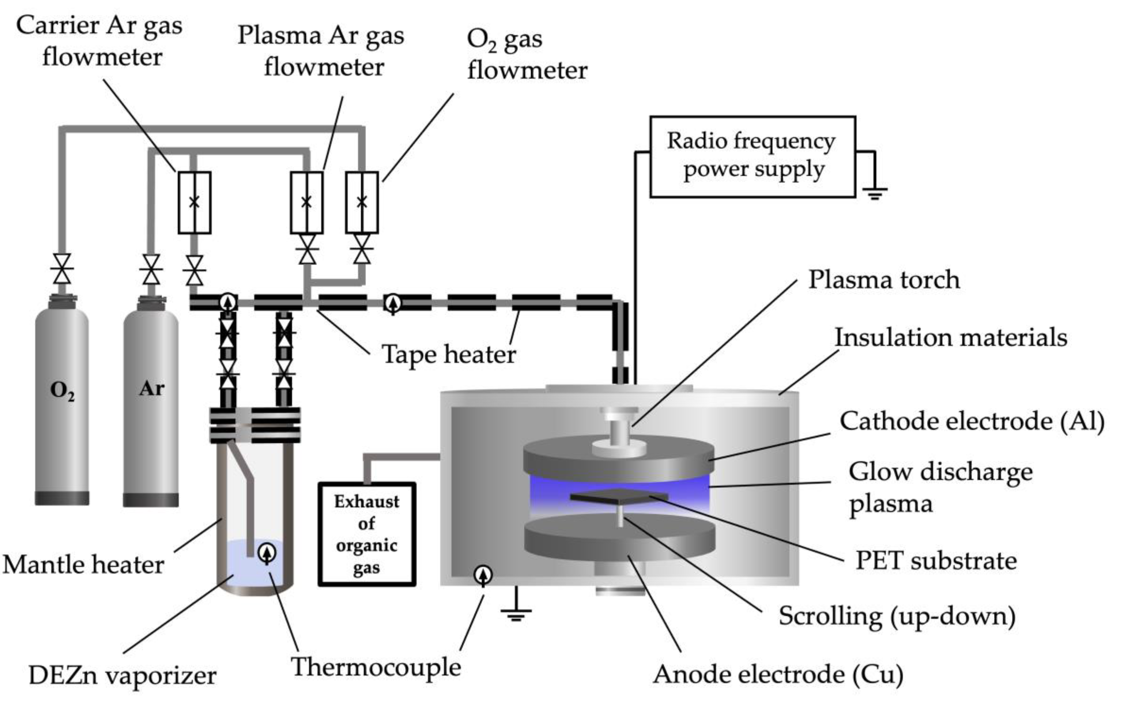
The fabrication system of the low-pressure, high-frequency plasma generator is illustrated in
Figure 1. The plasma generator comprises an Al cathode and a grounded anode of Cu plate. A reactor machine of AYUMI INDUSTRY Co., Ltd., Japan, was used a PET substrate with a cooling system placed on top of the anode plate. A slit type of hole (11 mm) is made to the cathode hole (105 mm) to let Ar + O
2 into the gap between the cathode and the anode. The anode plate scrolling with a PET substrate up and down in the direction perpendicular to the slit to produce flat films in a large area (scrolling distance: 25 mm). Atmospheric low-pressure high-frequency plasma was generated by flowing Ar as an insert gas with O
2 [
34,
35,
36,
37]. The reaction of O
2 and Ar ions (equation 1) is assumed to be the same as for mutual neutralization of oxygen ions [
38,
39].
The Ar carrier gas was fed through the inner space of the cathode down to the gap, where it was stimulated by the RF plasma generator (AX-3000, AD-TEC, Japan). Diethylzinc (C₂H₅)₂Zn or DEZn (Tri Chemical Laboratories Inc., Japan) was vaporized and carried by the Ar + O2 carrier gas flow into the plasma generated in the gap. When DEZn comes into contact with air, it burns to form zinc oxide (ZnO), carbon dioxide (CO2), and water (H2O). The reaction occurs when DEZn comes into contact with oxygen molecules. The balanced chemical equation is as follows.
To allow the chemical reaction that forms a thin film on the substrate surface to proceed at an acceptable rate. It is necessary to remove product product gasses from the deposition environment. A vacuum pump (EBARA DRY PUMP A30W, Ebara cooperation, Japan) was used, which corresponds to the reaction flow and chemical properties of the gases. According to the fabrication conditions for the film preparation, the parameters is listed in
Table 1.
2.2. Fabrication of DSSCs
The 1.5 cm x 1.5 cm ITO glass (Lumtec., Taiwan) with a sheet resistance of 9 to 15 Ω/sq applied as the photoanode substrate. The ZnO/PET was coated on the ITO glass to form a film using a screen printing technique. It was then immersed in a D102 dye solution (95% HPCL, Sigma-Aldrich) at room temperature for 12 hours to absorb dye molecules. After that, the films were rinsed with ethanol and dried. The DSSCs fabricated in the form sandwiching on ITO-based and ZnO/PET with an electrolyte 0.2 M PMII, 0.05 M I2, 0.1 M LiI, 0.2 M TBAI, 0.5 M, TBP in AN/VN [
40] as well as thick thermal-plastic Surlyn spacer (SX1170-25, Solaronix) was used.
2.3. Characterization
To investigate the ZnO thin film properties, Hall effect measurement (ECOPIA HMA-2000) and a four-point probe device (DASOL ENG FPP-HS-8) were used to measure the resistivity, carrier concentration, and mobility. A surface profilometer measured the film’s thickness (Dektak 150). A UV-VIS spectrophotometer (Hitachi, U-3000) was applied to analyze the optical transmittance spectra of ZnO thin films. Furthermore, the morphology of ZnO thin films deposited on the PET substrate was examined through the X-ray diffraction (XRD) (Rigaku D/max 2100H) technique. A field emission scanning electron microscope (FE-SEM: S-5500, HITACHI) machine was used to observe the structural properties of the films with the atomic force microscope (AFM: Prak, X-100).
3. Results
3.1. Physics of surface reaction under low-pressure high-frequency Ar + O2 plasma of ZnO film fabrication on PET substrate
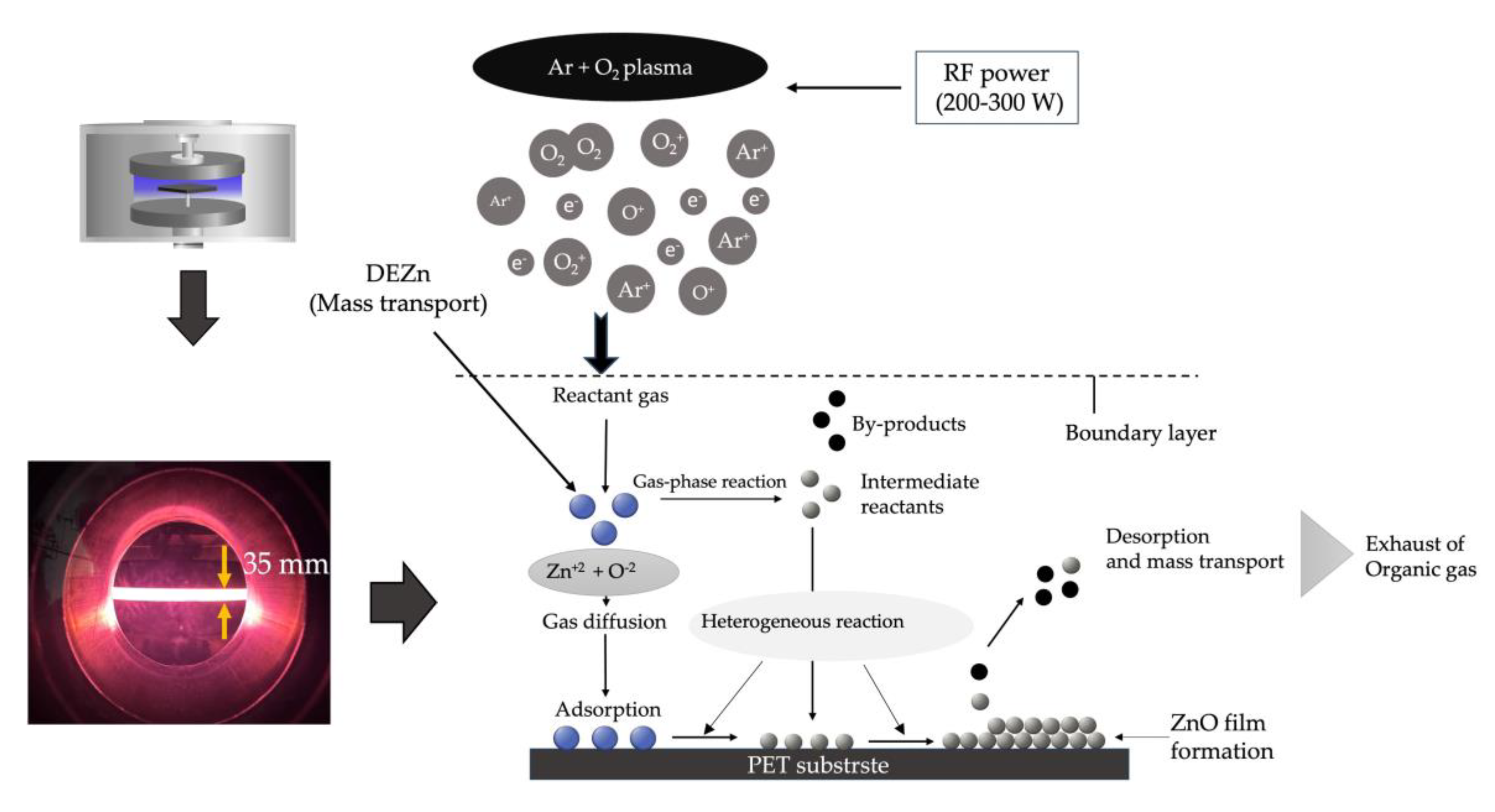
In
Figure 2, the process of chemical vapor deposition is illustrated. In the first stage, when precursor molecules of DEZn + O
2 + Ar enter the reactor chamber, Zn
+2 and O
-2 molecules are transported to the surface of a PET substrate through diffusion [
41] onto the substrate surface. After the reaction for the heterogeneous reaction [
42] on the surface, ZnO atoms remain. In contrast, the by-product molecules of the reaction on the substrate surface are adsorbed from the substrate to give the free gap for more Zn
+2 and O
-2 molecules to enter. In this research, we drive the reaction by increasing energy to the process of the Ar + O
2 plasma energy delivered to Zn
+2 and O
-2 molecules to increase the reaction rate to form ZnO precursor to the substrate surface. Under these conditions, the growth rate of the thin film depends only on the rate of chemical reactions on the substrate surface through plasma energy activation. The growth rate of the ZnO thin film is presented in terms of thickness in
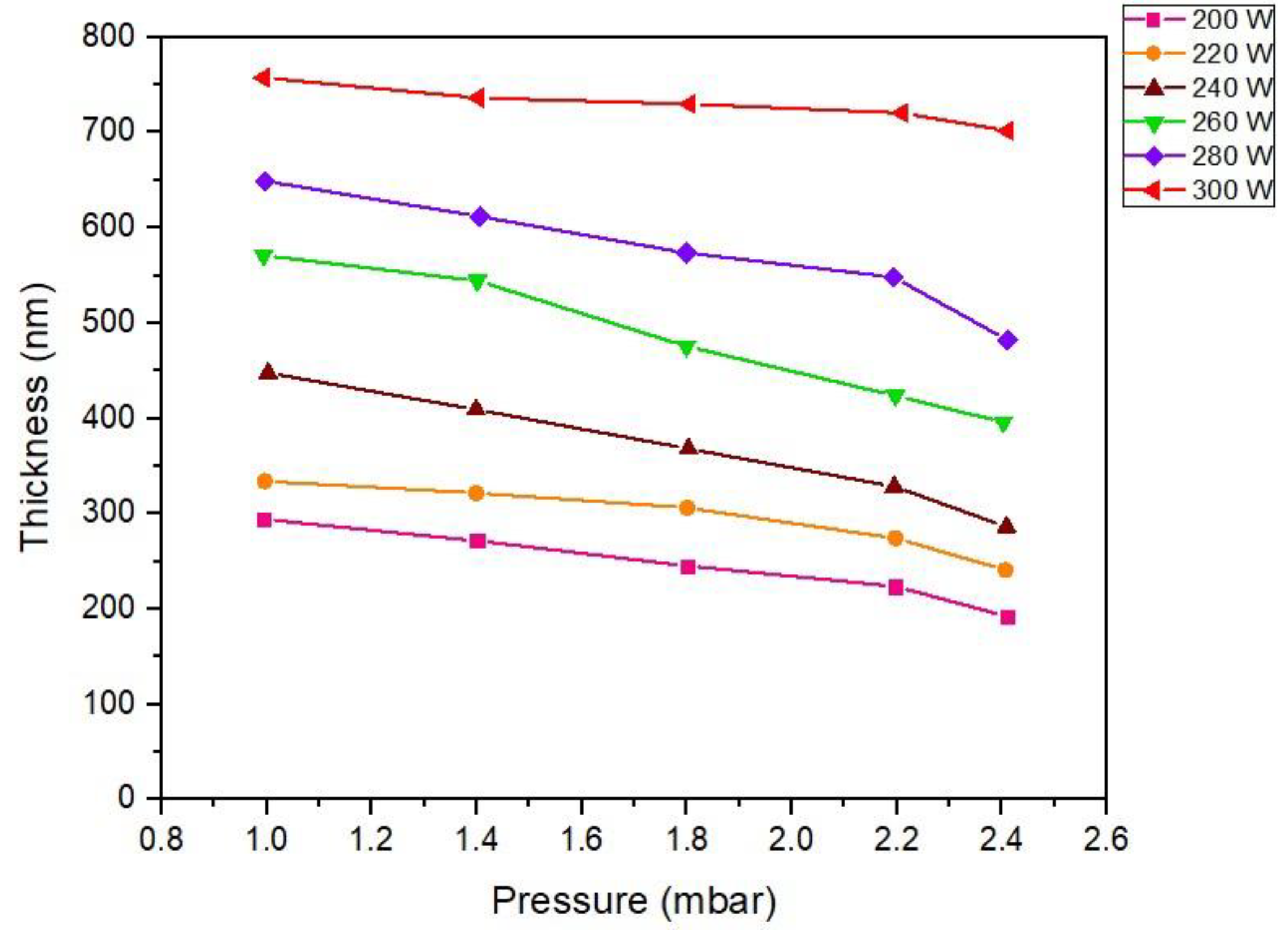
Figure 3.
3.2. Influence of RF power to the thickness of ZnO thin films
Under low-pressure, high-frequency Ar + O
2 plasma stimulated by gas phase collisions [
43] with RF power significantly influences the delivery of ZnO to the substrate surface. The reason is that most reaction chemical species produced in the plasma result in a much higher surface reaction rate [
44], resulting in differences in film thickness following different RF power supply activation conditions. In
Figure 3, the thickness of the ZnO film layer at different fabrication conditions of excitation with RF power 200-300 W is displayed. As can be seen in the graph, ZnO film prepared with RF power 300 W exhibits a maximum thickness greater than 700 nm. The reason is that the arrival rate of the ZnO precursor, also called precursor flux [
45], is higher than that of the other excitation conditions of RF power. As a result, the adsorption rate of ZnO molecules on the substrate is significant and directly proportional to the power supply condition of 200-300 W. However, if reaction by-products (
Figure 2) are still absorbed, they will prevent the arrival of the ZnO precursor, reducing the adsorption rate. The results can be observed at RF power 280-200 W, respectively, and increased pressure in the reactor chamber.
3.3. Structral properties of ZnO film deposited on PET substrates
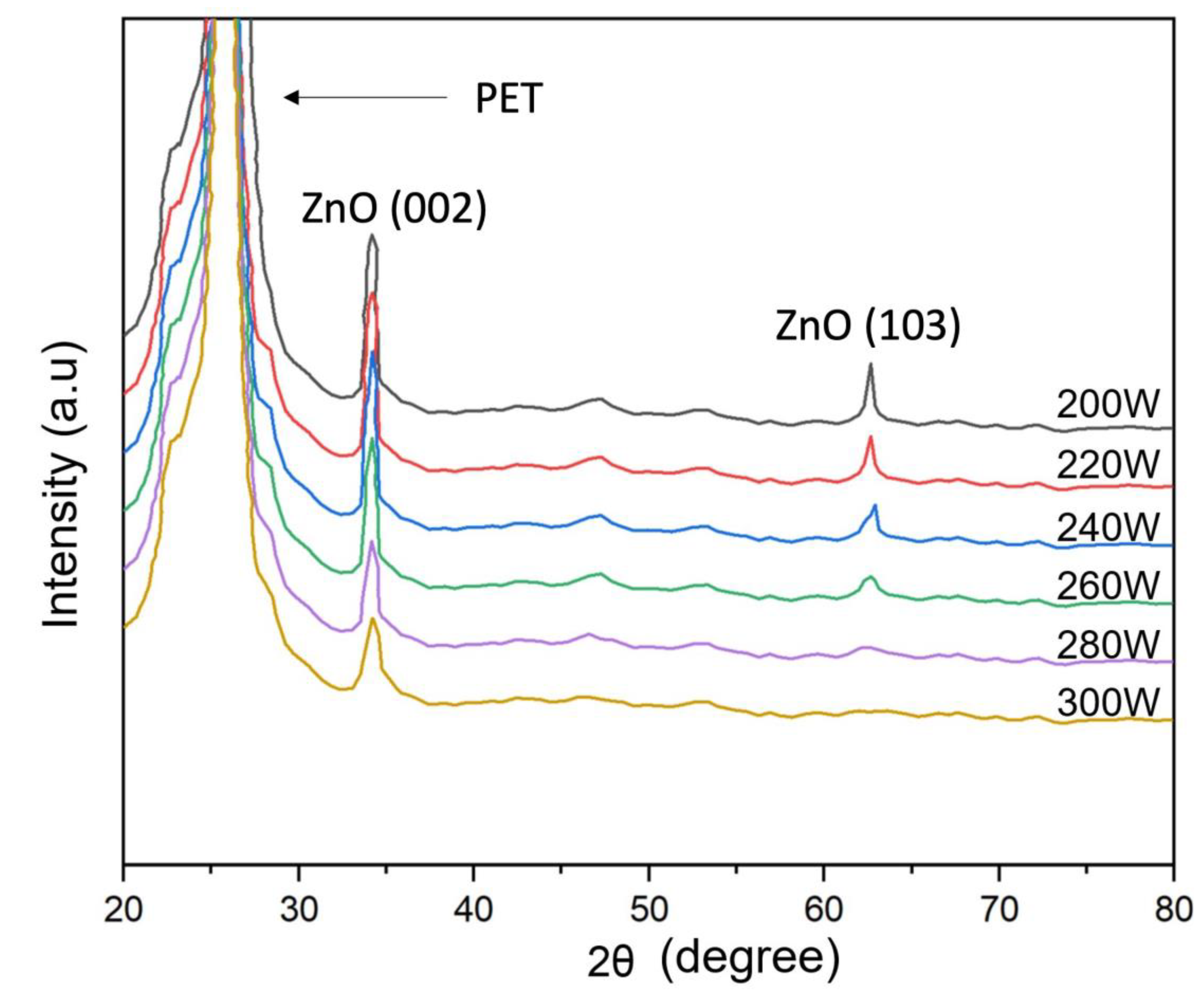
Figure 4 presents the XRD pattern of the ZnO film on the PET substrate under the diffraction pattern achieved with two from 20
to 80
. The information shows that the ZnO peaks detected are recognized as a polycrystalline hexagonal wurtzite crystal structure. The XRD spectra of all samples display ZnO (002) located at approximately 34.24
. This result is consistent with the previous study [
46,
47,
48]. Noticeably, the image information shows that as the RF power increased, the intensity of the diffraction peak (002) continuously rose, which increased the film thickness, consistent with
Figure 3. The small broad peak (103) is also observed. However, the diffraction intensity of (002) is more potent than that of (103) direction. According to the effect of film deposition with the ZnO film thickness result in
Figure 3, the results indicate that the ZnO thin film structure mainly appears with columnar grains structure pattern perpendicular to the substrate surface. Therefore, the research results show that the film thickness can change the crystal orientation of the ZnO film formation, which is directly affected by the plasma simulation of increasing RF power during the deposition process. For this reason, a suitable film thickness is required to create highly oriented ZnO crystalline thin films. The average crystalline size (D) of the ZnO film is determined using Scherrer’s equation [
49].
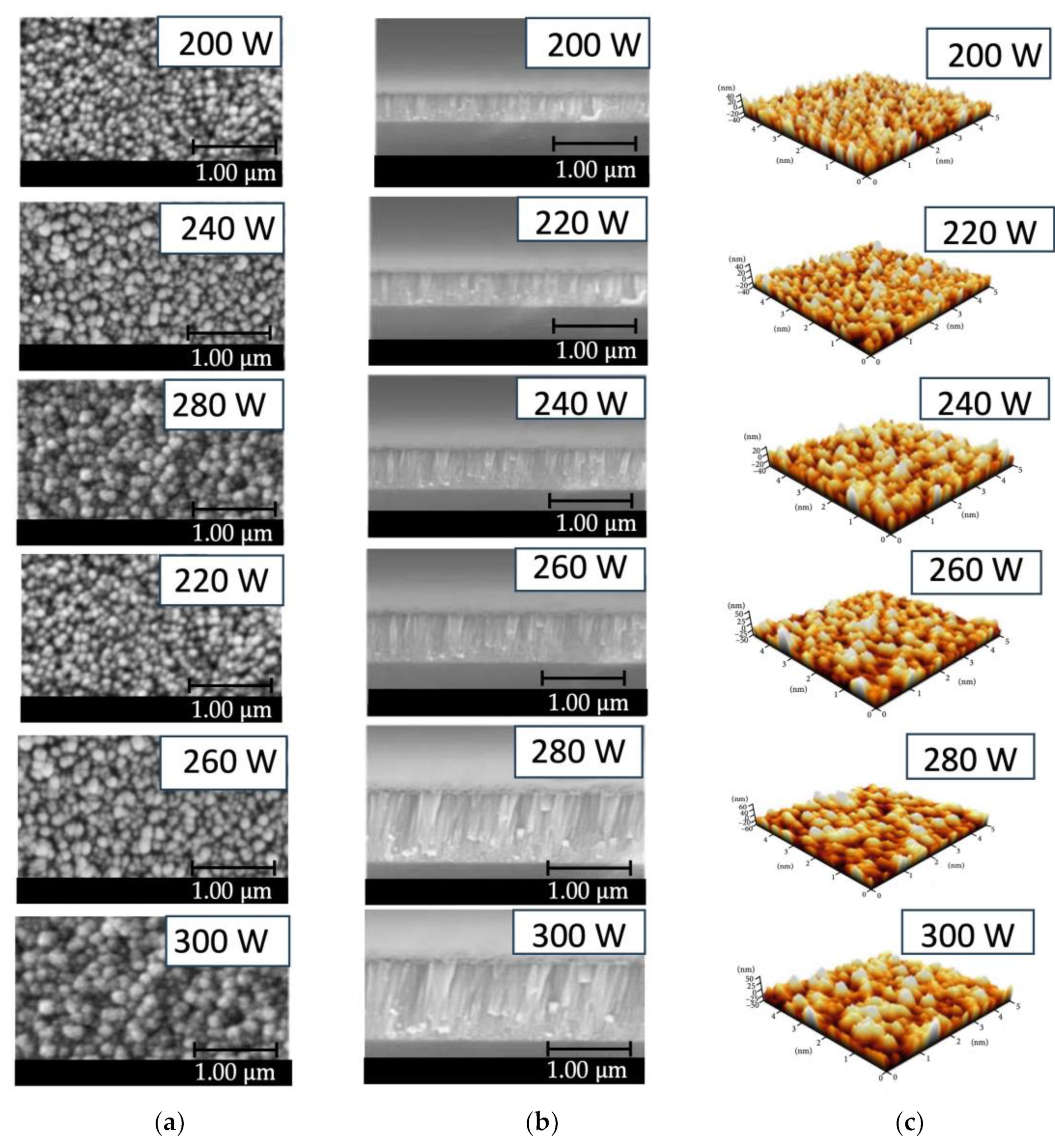
Figure 5(a-b) illustrates FE-SEM images consisting of a top view (5(a)) and cross-section view (5(b)) of ZnO thin film surface prepared with low-pressure high-frequency Ar + O
2 plasma chemical vapor deposition. The test results found that the ZnO film prepared with RF power 300 W had the characteristic of forming a dense and uniform columnar film with a thickness of 720 nm. The surface of the film has a granular structure. The grains are prominent in the 50-150 nm range, with an average of approximately 100 nm. According to the observation, plasma energy affects film formation. Where the RF power is low, the film is thin, the density is low, and the grain is small. When the RF power increases, the film has a dense columnar appearance. It is more uniform, and the film surface has a granular structure. The grain is larger and more defined. Thus, the FE-SEM images show that using low-pressure, high-frequency Ar + O
2 plasma to stimulate the production of ZnO thin films significantly affects film growth. For films with higher RF power, which has a significant energy content, the kinetic energy of ZnO atoms will increase, and the diffusion coefficient will also be high. In this case, it moves throughout the available space, causing large grains denser on the film. On the other hand, while preparing films with lower RF power, the kinetic energy of the ZnO atoms is low. It has a low diffusion coefficient, resulting in scattered clumps together sparsely, resulting in low deposition. It gives a columnar crystal structure with a low density. Additionally,
Figure 5(c) displays an AFM image of a ZnO film showing film surface characteristics consistent with the FE-SEM images in
Figure 5(a) and 5(b).
3.4. Electrical Properties
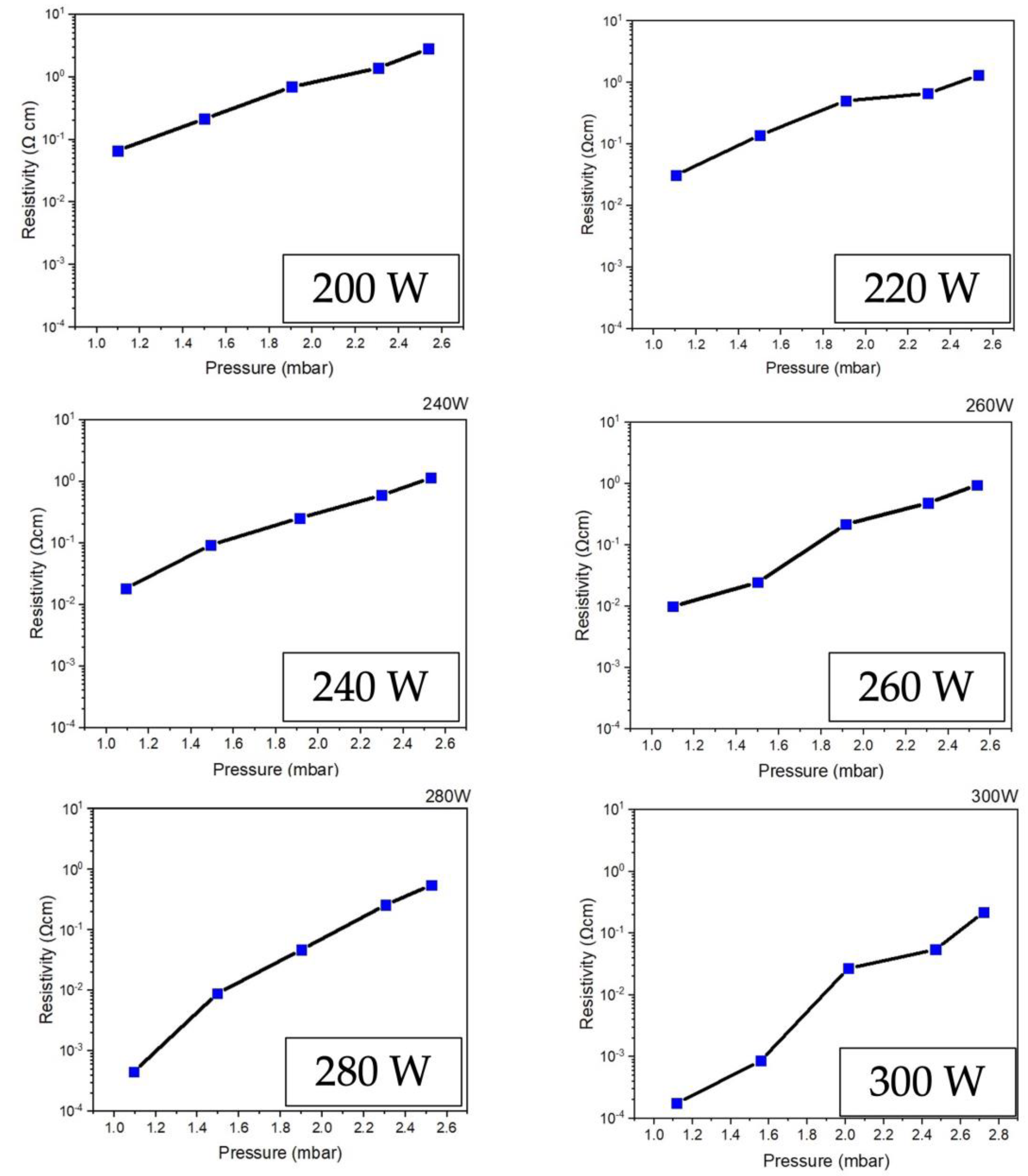
Figure 6 illustrates the comparative results of the electrical resistivity of ZnO films prepared with different plasma power excitation conditions of RF power 200-300 W. The trend of the graph shows that it is related to the ZnO film thickness investigation results in
Figure 3, which has the lowest electrical resistivity value of 1.8 x 10
-4 Ωcm under the condition of film preparation at RF power 300 W. This is because when stimulating the film depositing process with higher plasma energy, it will support the reaction between the precursors. Thus, the final product will obtain the thicker ZnO films with a smooth texture and consistency.
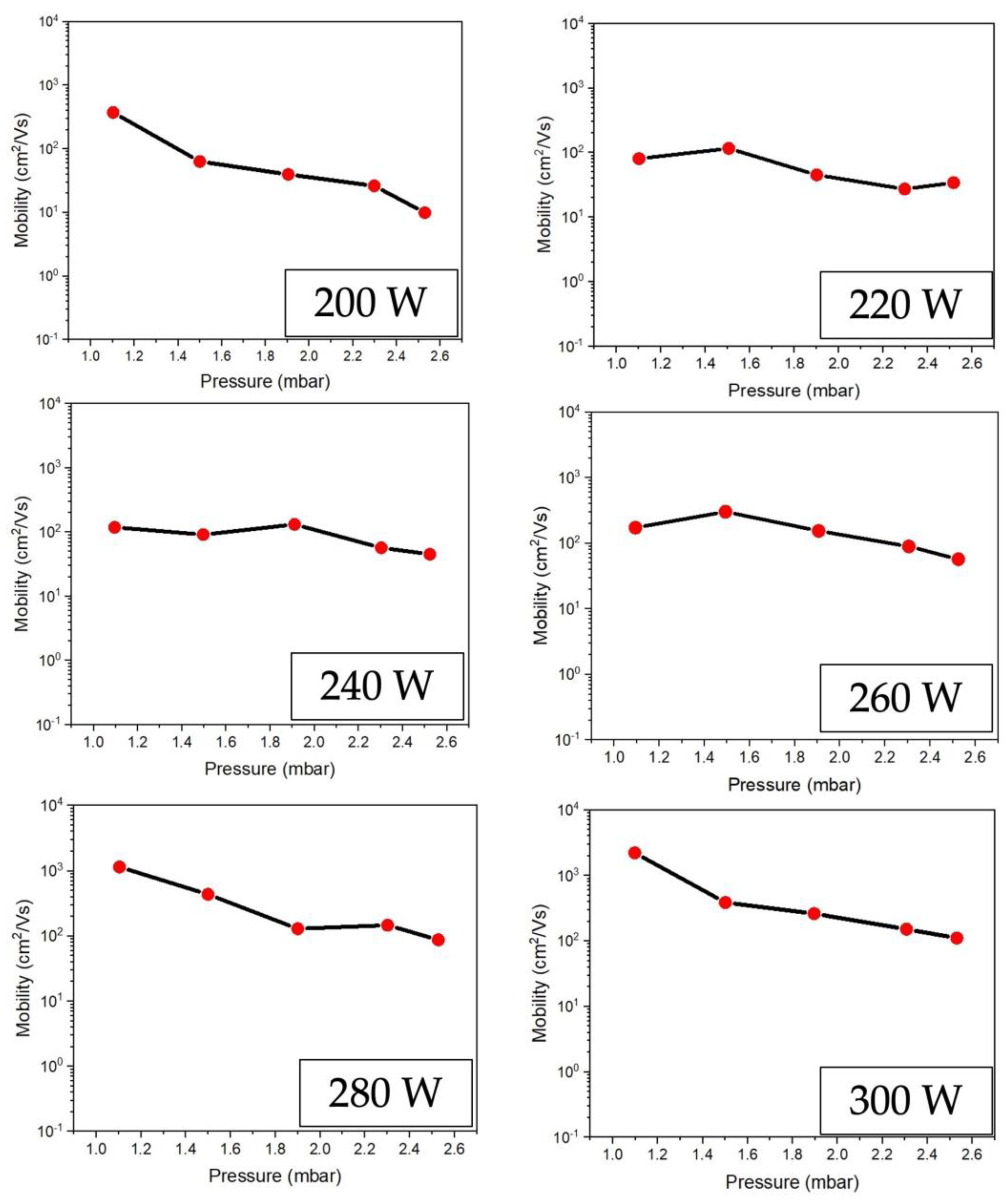
Figure 7 illustrates the comparison between carrier mobility and different conditions of RF power supply to ZnO fabrication. The results indicate that carrier mobility tends to decline as the RF power increases. It is inversely proportional to the electrical resistivity graph, as shown in
Figure 6. The result can be assumed that low electrical resistivity is shown when the carrier mobility is high.
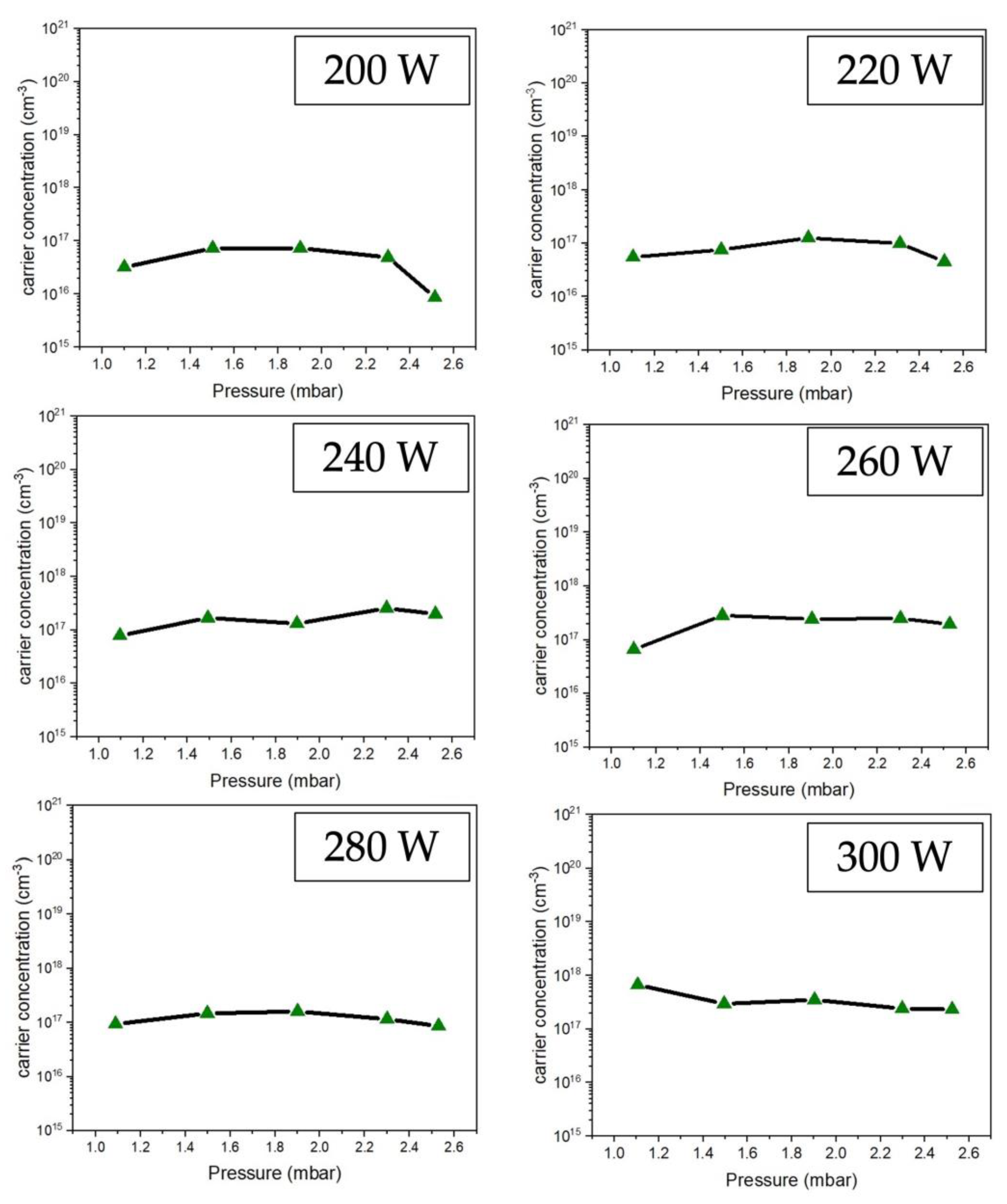
Figure 8 displays the effect of RF power on the carrier concentration. The results showed similar values, but 300 W gives a maximum carrier concentration of about 9.7 x 10
17 cm
-3.
Table 2 summarizes the result in each RF power supply case to make it easier to understand.
3.5. Transmittance Properties
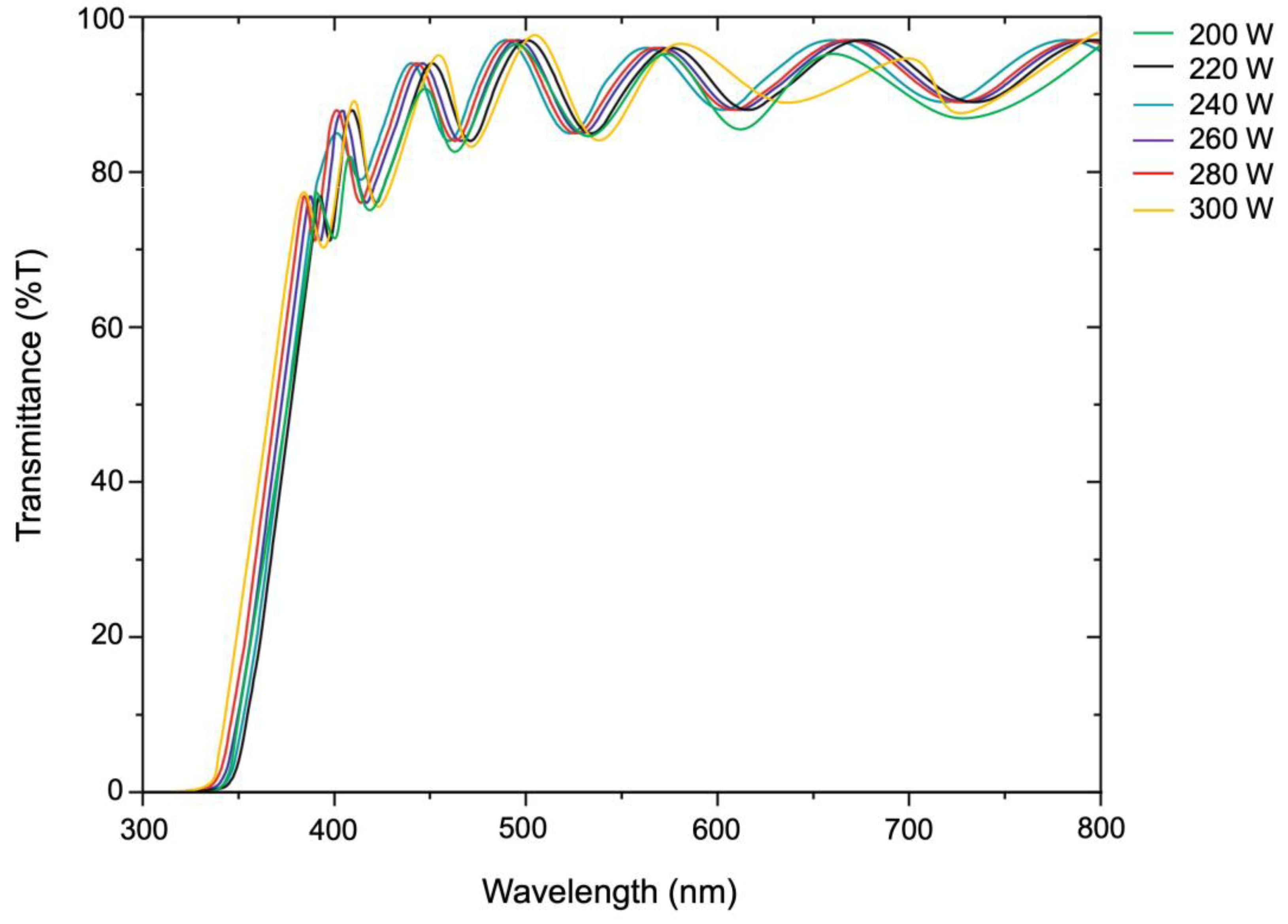
The light transmittance of the ZnO film was measured using a dual-beam UV-visible spectrometer, as shown in
Figure 9. The results showed that all samples had light transmission in the wavelength range of 400-800 nm. Due to the thickness of the films, the interference streaks that occurred were sine waves. When measuring the light transmittance, it appears as a precise sine wave. The average light transmittance percentage increased as the film thickness decreased. The reaction on the substrate surface in
Figure 1 explains the reason. Due to the lower plasma energy excited, the ZnO precursor is less likely to fall onto the substrate. As a result, the thickness of ZnO films will be less, increasing light transmittance.
3.6. Photovoltaic characterization of DSSCs
In this work, the parameters were determined to calculate the power conversion efficiency (PEC), which includes short circuit current density (
), open circuit voltage (
, maximum current density (
is the maximum electric current per area while the voltage is equal to zero, maximum potential (
is the voltage value when is no current or equal to zero and fill factor (FF) is the ratio between the multiple of maximum current density and maximum potential divided the multiple of short circuit current density and open circuit voltage [
50,
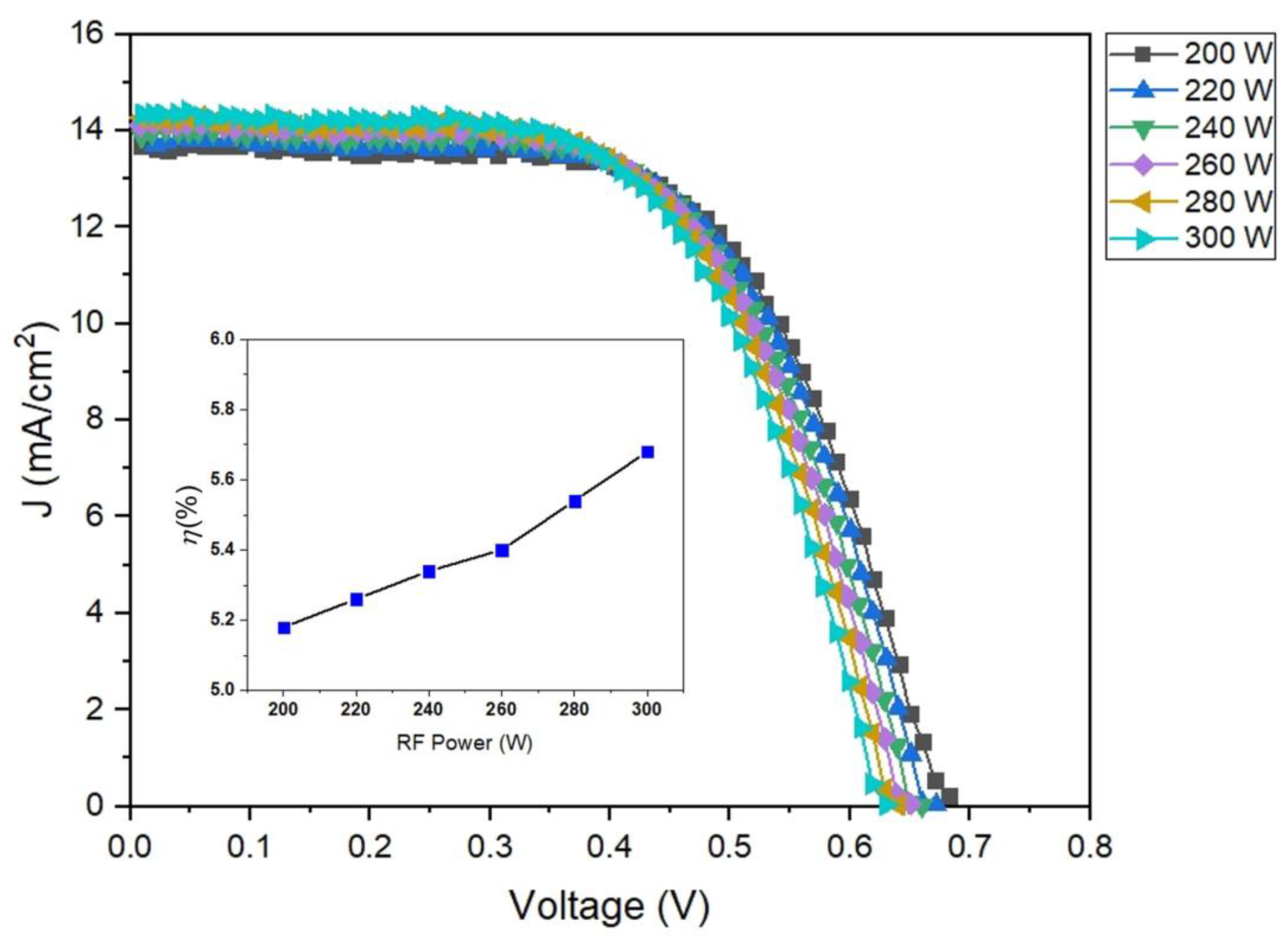
51], as shown the photocurrent density-photovoltage (J-V) curves of DSSCs in
Figure 10. Therefore, a power conversion efficiency (PCE) can be calculated by the multiple of
,
, and FF divided by an incident light power (
[
50,
51] as shown in Equation (4).
Figure 10 presents the power conversion efficiency of DSSCs based on ZnO/PET substrate by one sun illumination of AM 1.5 G with 100 mW/cm
2. The DSSCs with ZnO/PET of deposition conditions of RF power 300 W show a higher short circuit current density of 14.32 mA/cm2and improved FF value of 0.63 with an open-circuit voltage of 0.63 V in comparison with the other samples, which results in a high power conversion efficiency of 5.68%.
4. Discussion
The research found that a ZnO thin film was fabricated using low-pressure, high-frequency Ar + O2 plasma and the chemical vapor deposition technique from DEZn under different film formation conditions. This will produce films with different electrical properties, optical properties, and film surface characteristics. The results can be summarized as follows.
Firstly, in thin film production, when ZnO precursors generated by RF plasma excitation are adsorbed on the surface of a PET substrate. After that, decomposition will occur under heterogeneous reactions through interaction with the substrate surface. In this case, the DEZn, O2, and Ar molecules excited by RF power decompose to form ZnO atoms on the surface of the substrate, and Ar and O2 molecules are absorbed into the gas phase. The rate of degradation of Ar and O2 depends on the temperature and vacuum pressure in the film formation process. Thus, the surface reactions that create ZnO thin films in these deposition processes consume energy from high-energy chemicals produced using plasma, an RF plasma source. The reason is that free ions and electrons in the plasma can attack the growing film directly.
Second, when considering the RF power and vacuum pressure, the effect on the deposition and thickness of the ZnO films. As the pressure increased, the film thickness tended to decrease. This is because the number of argon ions in plasma generation will increase. When the vacuum pressure increases, the ZnO atoms collide with the argon ions in the plasma simulation system in the reaction chamber and then lose energy due to the collision, causing them not to have enough power to drop on the substrate. In this, the deposition rate will decrease. Meanwhile, ZnO film prepared with higher RF power resulted in a corresponding increase in film layer thickness. Due to the energy supply, increasing plasma production accelerates chemical reactions, resulting in high-energy collisions and momentum transfer between atoms. As a result, the atoms have high energy of movement while depositing onto the substrate. In this, the film with thicker film will be obtained than the sample prepared with low power.
Finally, vacuum pressure and RF power affect the film’s electrical resistivity and physical characteristics. As the vacuum pressure in the system increases, the electrical resistivity increases. As the RF power increases, the electrical resistance decreases. For this, both the carrier nobility and carrier density influence the electrical resistivity of the film. The increasing vacuum pressure in the system produces more positive ions in the plasma. In this, when positive ions collide with ZnO atoms, it has a chance of losing energy from colliding between ions, causing the kinetic energy of ZnO atoms to be reduced, with a low diffusion coefficient leading them to clump together into scattered clusters. These will result in a low deposition rate and a columnar crystal structure with a low density, resulting in a film with high electrical resistivity. However, adding plasma energy to the system through RF power will stimulate atoms with more deposition energy to have more kinetic energy and a high diffusion coefficient, creating a thick film layer and large grains.
5. Conclusions
The ZnO thin films are entirely fabricated by low-pressure, high-frequency Ar + O2 plasma using a chemical vapor deposition technique. Among the comparison of each sample under different RF power supplies 200, 220, 240, 260, 280, and 300 W, RF power 300 W exhibits the lowest electrical resistivity of 1.8 x 10⁻⁴ Ω-cm, which is the most comfortable property to apply in a DSSC device. At this point, the efficiency measurement is presented at 5.68%. Therefore, the results will be helpful in the solar cell manufacturing industry and provide a new way to create ZnO thin films for use as solar cells.
Author Contributions
Conceptualization, W.P. and T.Y.; methodology, N.K., N.M. and N.T.; software, N.K. and T.M.; validation, W.P. and T.Y.; formal analysis, W.P., K.T. and S.A..; investigation, N.K. and N.M.; resources, K.T. and T.Y.; data curation, T.T. and T.Y.; writing—original draft preparation, W.P. and T.Y.; writing—review and editing, W.P. and N.M.; visualization, N.K. and N.M.; supervision, N.K. and A.S.; project administration, N.K. and N.M.; funding acquisition, N.M. All authors have read and agreed to the published version of the manuscript.
Funding
This research was funded by the Royal Golden Jubilee (RGJ) Ph.D scholarship from the National Research Council of Thailand under the Ministry of Higher Education, Science, Research, and Innovation, grant number N41A650091.
Acknowledgments
The authors would like to thank School of Energy Environment and Materials under Energy Technology program, King Mongkut’s University of Technology Thonburi (KMUTT), Bangkok, Thailand. And a Collaborative Research Facility Station with Faculty of Education, University of Miyazaki, Miyazaki, Japan
Conflicts of Interest
The authors declare no conflicts of interest.
References
- Best research-cell efficiencies chart. Available online: https://www.nrel.gov/pv/cell-efficiency.html (accessed on 30 April 2024).
- Halme, J.; Vahermaa, P.; Miettunen, K.; Lund, P. Device Physics of Dye Solar Cells. Adv. Mater. 2010, 22, E210–E234. [Google Scholar] [CrossRef] [PubMed]
- Peter, L. M. Dye-sensitized nanocrystalline solar cells. Phys. Chem. Chem. Phys. 2007, 9, 2630–2642. [Google Scholar] [CrossRef] [PubMed]
- O’Regan, B.; Gratzel, M. A low-cost, high-efficiency solar cell based on dye-sensitized colloidal TiO2 films. Nature 1991, 353, 737–740. [Google Scholar] [CrossRef]
- Kalyanasundaram, K. Dye-sensitized solar cells, 1st ed.; EPFL: Lausanne, Switzerland, 2010; pp. 1–38. [Google Scholar]
- Noorasid, N.S.; Arith, F.; Mustafa, A.N.; Azam, M.A.; Mahalingam, S.; Chelvanathan, P.; Amin, N. Current advancement of flexible dye sensitized solar cell: A review. Optik 2022, 254, 168089. [Google Scholar] [CrossRef]
- Cavallo, C.; Di Pascasio, F.; Latini, A.; Bonomo, M.; Dini, D. Nanostructured semiconductor materials for dye-sensitized solar cells. J. Nanomater. 2017, 3, 1–31. [Google Scholar] [CrossRef]
- Chen, L.; Tan, W.; Zhang, J.; Zhou, X.; Zhang, X.; Lin, Y. Fabrication of high performance Pt counter electrodes on conductive plastic substrate for flexible dye-sensitized solar cells. Electrochim. Acta. 2010, 55, 3721–3726. [Google Scholar] [CrossRef]
- Weerasinghe, H.; Huang, F.; Cheng, Y.-B. Fabrication of flexible dye sensitized solar cells on plastic substrates. Nano energy 2013, 2, 174–189. [Google Scholar] [CrossRef]
- Su, H.; Zhang, M.; Chang, Y.-H.; Zhai, P.; Hau, N.Y.; Huang, Y.-T.; Liu, C.; Soh, A.K.; Feng, S.-P. Highly conductive and low cost Ni-PET flexible substrate for efficient dye-sensitized solar cells. ACS Appl. Mater. Interfaces. 2014, 6, 5577–5584. [Google Scholar] [CrossRef] [PubMed]
- Murali, B.; Gireesh Baiju, K.; Krishna Prasad, R.; Jayanarayanan, K.; Kumaresan, D. Fabrication of high-efficiency PET polymer-based flexible dye-sensitized solar cells and tapes via heat sink-supported thermal sintering of bilayer TiO2 photoanodes. Sustain. Energy Fuels. 2022, 6, 2503–2513. [Google Scholar] [CrossRef]
- Stranks, S.D.; E Eperson, G.; Grancini, G.; Menelaou, C.; J P Alcocer, M.; Leijtens, T.; M Herz, L.; Petrozza, A.; J Snaith, H. Electron-hole diffusion lengths exceeding 1 micrometer in an organometal trihalide perovskite absorber. Science 2013, 342, 341–344. [Google Scholar] [CrossRef]
- Anta, J.A.; Guillen, E.; Tena-Zaera, R. ZnO-based dye-sensitized solar cells. J. Phys. Chem. C 2012, 116, 11413–11425. [Google Scholar] [CrossRef]
- Vittal, R.; Ho, K.-C. Zinc oxide based dye-sensitized solar cells: A review. Renew. Sustain. Energy Rev. 2017, 70, 920–935. [Google Scholar] [CrossRef]
- Poonthong, W.; Mungkung, N.; Arunrungrusmi, S.; Yuji, T.; Sung, Y.-M. High performance of IZO coated on PET substrate for electroluminescence device using oxygen plasma treatment. Int. J. Photoenergy. 2021, 2021, 889002. [Google Scholar] [CrossRef]
- White, M. S.; Olson, D. C.; Shaheen, S. E.; Kopidakis, N.; Ginley, D. S. Inverted bulk-heterojunction organic photovoltaic device using a solution-derived ZnO underlayer. Appl. Phys. Lett. 2006, 89, 143517. [Google Scholar] [CrossRef]
- Waldauf, C.; Morana, M.; Denk, P.; Schilinsky, P.; Coakley, K.; A Choulis, S.; Brabec, C.J. Highly efficient inverted organic photovoltaics using solution based titanium oxide as electron selective contact. Appl. Phys. Lett. 2006, 89, 233517. [Google Scholar] [CrossRef]
- Ossai, A.N.; Alabi, A.B.; Ezike, S.C.; Aina, A.O. Zinc oxide-based dye-sensitized solar cells using natural and synthetic sensitizers. Curr. Res. Green Sustain. Chem. 2020, 3, 10043. [Google Scholar] [CrossRef]
- Thomas, D.G. Interstitial zinc in zinc oxide. J. Phys. Chem. Solids. 1957, 3, 229–237. [Google Scholar] [CrossRef]
- Harrison, S. E. Conductivity and hall effect of ZnO at low temperatures. Phys. Rev. 1954, 93, 52–62. [Google Scholar] [CrossRef]
- Hutson, A. R. Hall effect studies of doped zinc oxide single crystals. Phys. Rev. Res. 1957, 108, 222–230. [Google Scholar] [CrossRef]
- Ribut, S.H.; Abdullah, C.A.C.; Yusoff, M.Z.M. Investigation of structural and optical properties of zinc oxide thin films growth on various substrates. Results Phys. 2019, 13, 102146. [Google Scholar] [CrossRef]
- Faraj, M.G.; Ibrahim, K. Optical and structural properties of thermally evaporated zinc oxide thin films on polyethylene terephthalate substrates. Int. J. Polym. Sci. 2011. [Google Scholar] [CrossRef]
- Zhao, M.-J.; Sun, Z.-T.; Hsu, C.-H.; Huang, P.-H.; Zhang, X.-Y.; Wu, W.-Y.; Gao, P.; Qiu, Y.; Lien, S.-Y.; Zhu, W.-Z. Zinc oxide films with high transparency and crystallinity prepared by a low temperature spatial atomic layer deposition process. Nano-materials 2020, 10, 459. [Google Scholar] [CrossRef]
- Morosanu, C.E. Technique of preparing thin films. In Thin Films by Chemical Vapour Deposition, 1st ed.; Siddall, G.; Elsevier: New York, USA, Volume 7, pp. 31-54.
- Crowell, J.E. Chemical methods of thin film deposition: Chemical vapor deposition, atomic layer deposition, and related technologies. J. Vac. Sci. Technol. 2003, A 21, S88–S95. [Google Scholar] [CrossRef]
- Fay, S.; Kroll, U.; Bucher, C.; Vallat-Sauvain, E.; Shah, A. Low pressure chemical vapour deposition of ZnO layers for thin-film solar cells: temperature-induced morphological changes. Sol. Energy Mater. Sol. Cells 2005, 86, 385–397. [Google Scholar] [CrossRef]
- Liang, C.; Zhong, Y.; Zhong, Q.; Li, J.; Cao, W.; Wang, X.; Wang, S.; Xu, X.; Wang, J.; Cao, Y. Low-Temperature Deposition of High-Quality SiO2 Films with a Sloped Sidewall Profile for Vertical Step Coverage, Coatings 2022, 12, 1411. 12.
- Viguie, J.C.; Spitz, J. Chemical Vapor Deposition at Low Temperatures. J. Electrochem. Soc. 1975, 122, 585. [Google Scholar] [CrossRef]
- Dupuis, R.D.; Dapkus, P.D. Room-temperature operation of Ga(1−x)AlxAs/GaAs double-heterostructure lasers grown by metalorganic chemical vapor deposition. Appl. Phys. Lett. 1997, 31, 466–468. [Google Scholar] [CrossRef]
- Sterling, H.F.; Swann, R.C.G. Chemical vapour deposition promoted by r.f. discharge. Solid State Electron. 1965, 8, 653–654. [Google Scholar] [CrossRef]
- Kern, W.; Rosler, R. S. Advances in Deposition Processes for Passivation. J. Vac. Sci. Technol. 1977, 14, 1082. [Google Scholar] [CrossRef]
- Ullah, Z.; Riaz, S.; Li, Q.; Atiq, S.; Saleem, M.; Azhar, M.; Naseem, S.; Liu, L. A comparative study of graphene growth by APCVD, LPCVD and PECVD. Mater. Res. Express 2018, 5, 035606. [Google Scholar] [CrossRef]
- Gudmundsson, J.T.; Marakhtanov, A.M.; Patel, K.K.; Gopinath, V.P.; Lieberman, M.A. On the plasma parameters of a planar inductive oxygen discharge. J. Phys. D: Appl. Phys. 2000, 33, 1323. [Google Scholar] [CrossRef]
- Sun, X.; Bao, J.; Li, K.; D. Argyle, M.; Tan, G.; Adidharma, H.; Zhang, K.; Fan, M.; Ning, P. Advance in Using Plasma Technology for Modification or Fabrication of Carbon-Based Materials and Their Applications in Environ mental, Material, and Energy Fields. Adv. Funct. Mater. 2021, 31, 2006287. [Google Scholar] [CrossRef]
- Gudmundsson, J.T.; Thorsteinsson. E.G. Oxygen discharges diluted with argon: dissociation processes. Plasma Sources Sci. Technol. 2007, 16, 399–412. [Google Scholar] [CrossRef]
- Cioffi, M.O.H.; Voorwald, H.J.C.; Mata, R.P. Surface energy increase of oxygen-plasma-treated PET. Mater. Charact. 2003, 50, 209–215. [Google Scholar] [CrossRef]
- Schofield, K. Rate constants for the gaseous interaction of O(21D2) and O(21S0 - a critical evaluation. J. Photochem 1978, 9, 55–68. [Google Scholar] [CrossRef]
- King, D.L.; Piper, L.G.; Setser, D.W. Electronic energy transfer from metastable argon (4s3P2,0) to xenon, oxygen and chlorine atoms. J. Chem. Soc., Faraday Trans. 2 1977, 73, 177–200. [Google Scholar] [CrossRef]
- Su, H.; Zhang, M.; Chang, Y.-H.; Zhai, P.; Hau, N.Y.; Huang, Y.-T.; Liu, C.; Soh, A.K.; Feng, S.P. Highly conductive and low cost Ni-PET flexible substrate for efficient dye-sensitized solar cells. ACS Appl. Mater. Interfaces 2014, 6, 5577–5584. [Google Scholar] [CrossRef] [PubMed]
- Bloem, J. Gas phase diffusion and surface reactions in the chemical vapour deposition of silicon. Pure & Appl. Chem. 1978, 50, 435–447. [Google Scholar]
- Jagur-Grodzinski, J. Heterogeneous Modification of Polymers: Matrix and Surface Reactions, 1st ed.; Wiley: USA, 1997; pp. 1–121. [Google Scholar]
- Shi, Y. Hot Wire Chemical Vapor Deposition Chemistry in the Gas Phase and on the Catalyst Surface with Organosilicon Compounds. Acc. Chem. Res. 2015, 48, 163–173. [Google Scholar] [CrossRef]
- Pollard, R.; Wang, Y.-F. An Approach for Modeling Surface Reaction Kinetics in Chemical Vapor Deposition Processes. J. Electrochem. Soc. 1995, 142, 1712. [Google Scholar]
- Vijay, A.; Mukhopadhyaya, A.; Shrivastava, V.; Bhardwaj, D.; Ganguli, A.K.; Ali, Md. E.; Vaidya, S. Understanding the role of ionic flux on the polarity of the exposed surfaces of ZnO. Phys. Chem. Chem. Phys. 2020, 22, 15427–15436. [Google Scholar] [CrossRef]
- Ribut, S.H.; Abdullah, C.A.C.; Yusoff, M.Z.M. Investigations of structural and optical properties of zinc oxide thin films growth on various substartes. Results Phys. 2019, 13, 102146. [Google Scholar] [CrossRef]
- Hu, S.Y.; Lee, Y.C.; Lee, J.W.; Huang, J.C.; Shen, J.L.; Water, W. The structural and optical properties of ZnO/Si thin films by RTA treatments. Appl. Surf. Sci. 2008, 254, 1578–1582. [Google Scholar] [CrossRef]
- Yang, R.-. Y, Weng, M.-H.; Pan, C.-T.; Hsiung, C.M.; Huang, C.C. Low-temperature deposited ZnO thin films on the flexible substrate by cathodic vacuum arc technology. Appl. Surf. Sci. 2011, 257, 7119–7122. [Google Scholar] [CrossRef]
- Khun, K.; Ibupoto, Z.; AlSalhi, M.; Atif, M.; Ansari, A.; Willander, M. Fabrication of well-aligned ZnO nanorods using a composite seed layer of ZnO nanoparticles and chi-tosan polymer. Materials 2013, 6, 4361–4374. [Google Scholar] [CrossRef] [PubMed]
- Qi, B.; Wang, J. Fill factor in organic solar cells. Phys. Chem. Chem. Phys. 2013, 15, 8972–8982. [Google Scholar] [CrossRef]
- Winder, C.; Saricftci, N.Z. Low bandgap polymers for photon harvesting in bulk heterojunction solar cells. J. Mater. Chem. 2004, 14, 1077–1086. [Google Scholar] [CrossRef]
Figure 1.
Equipment used in the low-pressure high-frequency Ar + O2 plasma using chemical vapor deposition technique of ZnO film fabrication on PET substrates.
Figure 1.
Equipment used in the low-pressure high-frequency Ar + O2 plasma using chemical vapor deposition technique of ZnO film fabrication on PET substrates.
Figure 2.
Reaction systems involving clusters of ZnO film formation under low-pressure high-frequency plasma stimulation by low-pressure high-frequency Ar + O2 plasma chemical vapor deposition on a PET substrate.
Figure 2.
Reaction systems involving clusters of ZnO film formation under low-pressure high-frequency plasma stimulation by low-pressure high-frequency Ar + O2 plasma chemical vapor deposition on a PET substrate.
Figure 3.
Influence of the variation RF power on ZnO film thickness preparing by low-pressure high-frequency Ar + O2 plasma chemical vapor deposition technique.
Figure 3.
Influence of the variation RF power on ZnO film thickness preparing by low-pressure high-frequency Ar + O2 plasma chemical vapor deposition technique.
Figure 4.
X-Ray diffraction analysis (XRD) of ZnO thin film deposited on a PET substrate preparing by low-pressure high-frequency Ar + O2 plasma chemical vapor deposition.
Figure 4.
X-Ray diffraction analysis (XRD) of ZnO thin film deposited on a PET substrate preparing by low-pressure high-frequency Ar + O2 plasma chemical vapor deposition.
Figure 5.
Microstructure image of the ZnO thin film deposited on PET substrate under different conditions of RF power 200-300 W preparing by low-pressure high-frequency Ar + O2 plasma chemical vapor deposition: (a) FE-SEM images of top-view; (b) FE-SEM images of cross-section view; (c) AFM images.
Figure 5.
Microstructure image of the ZnO thin film deposited on PET substrate under different conditions of RF power 200-300 W preparing by low-pressure high-frequency Ar + O2 plasma chemical vapor deposition: (a) FE-SEM images of top-view; (b) FE-SEM images of cross-section view; (c) AFM images.
Figure 6.
Electrical resistivity of ZnO thin film deposited on PET substrate comparing by different low-pressure high-frequency Ar + O2 plasma supply of RF power 200-300 W.
Figure 6.
Electrical resistivity of ZnO thin film deposited on PET substrate comparing by different low-pressure high-frequency Ar + O2 plasma supply of RF power 200-300 W.
Figure 7.
Comparison the carrier mobility on ZnO thin film preparing at different conditions of RF power 200-300 W under low-pressure high-frequency Ar + O2 plasma of chemical vapor deposition.
Figure 7.
Comparison the carrier mobility on ZnO thin film preparing at different conditions of RF power 200-300 W under low-pressure high-frequency Ar + O2 plasma of chemical vapor deposition.
Figure 8.
Comparison the carrier concentration on ZnO thin film preparing at different conditions of RF power 200-300 W under low-pressure high-frequency Ar + O2 plasma of chemical vapor deposition.
Figure 8.
Comparison the carrier concentration on ZnO thin film preparing at different conditions of RF power 200-300 W under low-pressure high-frequency Ar + O2 plasma of chemical vapor deposition.
Figure 9.
Light-transmittance of ZnO thin film deposited on PET substrate preparing by low-pressure high-frequency Ar + O2 plasma chemical vapor deposition under different conditions of RF power 200-300 W.
Figure 9.
Light-transmittance of ZnO thin film deposited on PET substrate preparing by low-pressure high-frequency Ar + O2 plasma chemical vapor deposition under different conditions of RF power 200-300 W.
Figure 10.
Photocurrent density-photovoltage (J-V) curves of DSSCs based on ZnO/PET substrates.
Figure 10.
Photocurrent density-photovoltage (J-V) curves of DSSCs based on ZnO/PET substrates.
Table 1.
Fabrication conditions of ZnO thin films deposited on PET substrate by low-pressure high-frequency plasma deposition technique.
Table 1.
Fabrication conditions of ZnO thin films deposited on PET substrate by low-pressure high-frequency plasma deposition technique.
| Source and Materials |
Conditions |
| Substrate |
PET |
Source material
|
DEZn of Tri Chemical Laboratories Inc. |
| Carrier Ar gas flow rate |
20 L/min |
| O2 gas flow rate |
0.5 L/min |
| RF plasma generator |
200-300 W |
| Scrolling distance |
25 mm |
| Anode and cathode gap |
35 mm |
Table 2.
The comparison of electrical properties on ZnO thin films deposited on PET substrates including resistivity, mobility, and carrier concentration under different RF power supply.
Table 2.
The comparison of electrical properties on ZnO thin films deposited on PET substrates including resistivity, mobility, and carrier concentration under different RF power supply.
RF power
(W) |
Resistivity
(Ω-cm) |
s) |
Carrier concentration
(cm-3) |
| lowest |
highest |
lowest |
highest |
lowest |
highest |
| 200 |
7.2 x 10⁻²
|
1.7 |
1.2 x 101
|
3.1 x 10²
|
7.6 x 10¹⁵
|
1.5 x 10¹⁶
|
| 220 |
2.2 x 10⁻²
|
1.1 |
4.1 x 101
|
1.1 x 10²
|
3.2 x 10¹⁶
|
8.5 x 10¹⁶
|
| 240 |
1.7 x 10⁻²
|
7.3 x 10⁻¹
|
4.6 |
1.8 x 10²
|
9.7 x 10¹⁶
|
2.3 x 10¹⁷
|
| 260 |
1.2 x 10⁻²
|
9.2 x 10⁻¹
|
7.4 |
1.2 x 10²
|
8.3 x 10¹⁶
|
2.2 x 10¹⁷
|
| 280 |
5.1 x 10⁻⁴
|
6.4 x 10⁻¹
|
9.8 |
1.2 x 10³
|
8.9 x 10¹⁶
|
1.7 x 10¹⁷
|
| 300*
|
1.8 x 10⁻⁴
|
3.1 x 10⁻¹
|
1.2 x 10²
|
2.1 x 10³
|
2.3 x 10¹⁷
|
9.7 x 10¹⁷
|
Table 3.
Photovoltaic parameters of DSSCs based on the ZnO/PET substrates of varying RF power 200-300 W.
Table 3.
Photovoltaic parameters of DSSCs based on the ZnO/PET substrates of varying RF power 200-300 W.
| ZnO/PET substrate |
(mA/cm-2) |
(V) |
FF |
, %)
|
| RF 200 W |
13.66 |
0.69 |
0.55 |
5.18 |
| RF 220 W |
13.78 |
0.67 |
0.57 |
5.26 |
| RF 240 W |
13.95 |
0.66 |
0.58 |
5.34 |
| RF 260 W |
14.10 |
0.65 |
0.59 |
5.40 |
| RF 280 W |
14.21 |
0.64 |
0.61 |
5.54 |
| RF 300 W |
14.32 |
0.63 |
0.63 |
5.68 |
|
Disclaimer/Publisher’s Note: The statements, opinions and data contained in all publications are solely those of the individual author(s) and contributor(s) and not of MDPI and/or the editor(s). MDPI and/or the editor(s) disclaim responsibility for any injury to people or property resulting from any ideas, methods, instructions or products referred to in the content. |
© 2024 by the authors. Licensee MDPI, Basel, Switzerland. This article is an open access article distributed under the terms and conditions of the Creative Commons Attribution (CC BY) license (http://creativecommons.org/licenses/by/4.0/).
