
Submitted:
19 July 2024
Posted:
19 July 2024
You are already at the latest version
Abstract
A spike-timing-dependent-plasticity (STDP) device with a Ga-Sn-O (GTO) conductance change layer deposited by a mist-CVD method has been developed. First, the memristive characteristic is analyzed. Next, based on it, spike waveforms are determined. Finally, the STDP characteristic is successfully confirmed. This is the first report on the realization of a STDP characteristic using a thin film deposited by the mist-CVD method, which is achieved by the GTO properties and a well-designed clear methodology to realize a STDP characteristic from a memristive characteristic.
Keywords:
spike-timing-dependent-plasticity (STDP)
; Ga-Sn-O (GTO)
; mist-CVD
; memristive characteristic
1. Introduction
Artificial intelligence (AI) provides critical infrastructures in modern and future societies through diverse applications [1,2]. Neural networks are the most popular embodiments of AI that mimic the operating theories of living brains [3,4]. However, traditional models of neural networks are large and complex software that runs on high-spec and energy-consuming hardware such as Neumann-type digital computers, which is not customized for neural networks [5,6]. Neuromorphic systems are practical solutions that consist only of customized devices, circuits, and hardware for neural networks with compact computer size and lower energy consumption [7,8]. Memristors are emerging devices that can be used as not only digital memories in old-fashioned computers [9,10] but also analog memories in neuromorphic systems [11,12,13,14,15,16,17,18,19,20]. However, once memristors are integrated into neuromorphic systems as computing in memory (CIM) or processing in memory (PIM) [21], it is considerably difficult to integrate also control circuits to adjust electrical conductivities because they are likely more complicated than neuromorphic systems themselves to generate arbitrary voltage or current. Therefore, autonomous learning is strongly desired. Incidentally, spiking neuromorphic systems are notable schemes as extremely low-energy systems, where spike pulses are utilized to send signals [22]. Spike-timing-dependent-plasticity (STDP) devices are inspired by biomimetic approach from living brains and promising to enable autonomous learning in spiking neuromorphic systems, and STDP characteristics are often realized as more advanced utilizations of memristor characteristics [23,24,25,26,27]. However, it was sometimes difficult to realize them, because there are many candidates of component materials, device structures, fabrication processes, driving schemes, etc.
Semiconductor materials are key-points for actual fabrication of memristors. Amorphous metal-oxide semiconductors (AOS) are semiconductor materials using common and inexpensive atomic elements and can exhibit excellent characteristics even if they are deposited at low temperatures, and therefore they are superior in low material and fabrication cost [28]. On the other hand, deposition methods are other key-points for actual fabrication of memristors. Mist chemical vapor deposition (CVD) methods are deposition methods in atmosphere pressure, and they are also superior in low fabrication cost [29,30]. However, it was not reported that the STDP device is realized with an AOS thin film deposited by the mist-CVD method.
In this research, a STDP device with a Ga-Sn-O (GTO) conductance change layer deposited by a mist-CVD method has been developed. GTO is one of the AOS and superior in further low material cost, non-toxicity, etc [31,32]. The device details, fabrication processes, memristive characteristics, spike waveforms, and STDP characteristic will be explained. This is the first report on the well-designed combination of the STDP, GTO, and mist-CVD technologies, and provides a clear methodology to realize a STDP characteristic from a memristive characteristic.
2. STDP Device with the GTO Conductance Change Layer Deposited by the Mist-CVD Method
The STDP device with the GTO conductance change layer deposited by the mist-CVD method is shown in Figure 1. First, the device structure and fabrication processes are shown in Figure 1a. A quartz substrate of the size of 15 mm × 15 mm and thickness of 0.7 mm is used, and an Al thin film is deposited using a vacuum evaporation method as a bottom electrode. Next, the hot-wall-type mist-CVD method is shown in Figure 1b. The GTO thin film is deposited using the mist-CVD method as a conductance change layer. Ga acetylacetonate (Ga(acac)) of 0.0855 g and Sn acetylacetonate (Sn(acac)) of 0.3324 g are dissolved in HCl of 20% and 3 g and pure water of 20 mL, whose volumes are adjusted so that the atomic composition is Ga:Sn = 1:4.5 in the solution. A mist of the solution is generated by ultrasonic generators, carried by a carrier gas of air of the flow rate of 1 L/min, diluted by a dilution gas of air of the flow rate of 1 L/min, and injected through a quartz tube, and the inside of the quartz tube is heated to the temperature of 450 °C by a heater. The GTO thin film is deposited during the deposition time of 30 min to the film thickness of 33 nm. Finally, a Au thin film is deposited using a vacuum evaporation method as a top electrode. The device structure is quite simple, namely, the GTO thin film is just sandwiched between the top and bottom electrodes.
3. Memristive Characteristic
The memristive characteristic is shown in Figure 2. First the hysteresis characteristic is shown in Figure 2a. Here, the bottom electrode is grounded, and an applied voltage to the top electrode (V) is scanned to 0 ~ -4.5 V ~ 0 as a reset operation. Then, V is scanned to 0 ~ +Vset ~ 0 with varying Vset = 2 ~ 4 V as set operations, and the flowing current (I) is measured. The magnified graph is also superimposed when V is 0 ~ 1 V. It is found that the set operation induces the transition from a low conductance state (LCS) to a high conductance state (HCS), whereas the reset operation initializes the electrical conductance. The hysteresis curve is observed, and the width of the hysteresis increases as Vset increases. Next, the switching ratio is shown in Figure 2b. Here, the switching ratio is defined as the conductance ratio between the HCS and LCS for V = 0.5 V. It is analyzed that the switching ratio remains the same below Vset ≦ 3 V and increases as Vset increases above Vset ≧ 3.5 V. The endurance and retention characteristics are under estimation and seems not so bad [33], so we would like to report them in the near future. The switching mechanism is also shown in [33].
4. Spike Waveforms
Based on the memristive characteristic shown in Figure 2b, spike waveforms are determined. The spike waveforms are shown in Figure 3a. First, pre-spike voltage (Vpre), post-spike voltage (Vpost), and net voltage (Vnet) are shown in Figure 3a. Here, Vpre is the voltage supposed to be applied to the top electrode, Vpost is that to the bottom electrode, Vnet = Vpre – Vpost is that to the STDP device. Δt is defined as the time lag between the Vpre and Vpost, and the spike waveforms for Δt = -0.2, 0, and +0.2 ms are shown as examples. Next, the maximum voltage of the Vnet (Vmax) is shown in Figure 3b. It is found that the Vmax ranges from Vmax ≦ 3 V to Vmax ≧ 3.5 V. Conversely speaking, the spike waveforms are well-designed so that the Vmax is so. As a result, it is expected that the device conductance remains the same or increases depending on the Δt.
5. STDP Characteristic
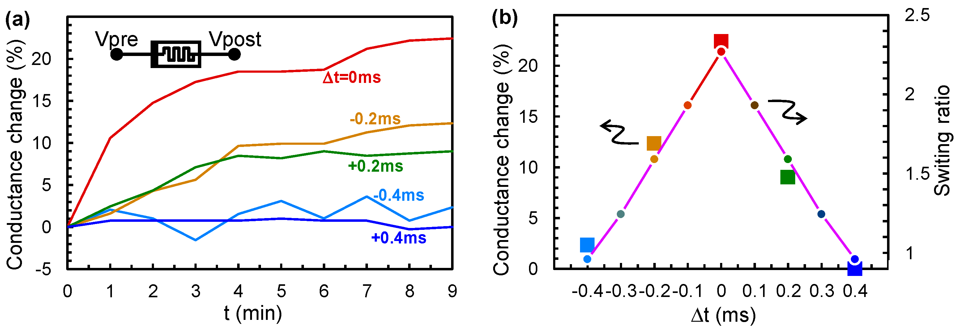
The STDP Characteristic is shown in Figure 4. The conductance change along time (t) is shown in Figure 4a. Here, the Vpre and Vpost shown in Figure 3a are actually applied to the top and bottom electrodes, respectively, with the frequency of 2 kHz, and the device conductance is measured in situ because small bias is applied when no spike pulse is applied as shown in Figure 3a. The conductance change is calculated as the change from the initial value. It is found that the device conductance almost remains the same for Δt = ±0.4 ms, increases for Δt = ±0.2 ms, and further increases for Δt = 0 ms, which is as expected. Next, the conductance change and switching ratio are shown in Figure 4b. Here, the conductance change is obtained from that for t = 9 min in Figure 4a, because it seems to roughly saturate, and the switching ratio is calculated by relating the Vset shown in Figure 2b and Vmax shown in Figure 3b. For example, Vmax = 3.7 V for Δt = 0.2 ms in Figure 3b, and the switching ratio is read as 1.59 for this Vmax in Figure 2b. It is found that the tendency of the conductance change is quite similar to that of the switching ratio, which is as expected. As a result, the STDP characteristic is successfully confirmed.
6. Conclusion
A STDP device with a GTO conductance change layer deposited by a mist-CVD method has been developed. First, the memristive characteristic was analyzed. Next, based on it, spike waveforms were determined. Finally, the STDP characteristic was successfully confirmed. This is the first report on the realization of a STDP characteristic using a thin film deposited by the mist-CVD method, which is achieved by the GTO properties and a well-designed clear methodology to realize a STDP characteristic from a memristive characteristic. In other words, it was proposed how to realize the STDP characteristic from the memristive characteristic, which will be useful for all future researchers who would like to apply their memristive devices to STDP devices. We expect that not only STDP devices we develop but also those other researchers develop can find possible applications for neuromorphic systems.
Author Contributions
Conceptualization, H.K. (Hidehito Kita) and M.K.; methodology, H.K. (Hidehito Kita) and K.U.; software, H.K. (Hidehito Kita); validation, H.K. (Hidenori Kawanishi) and M.K.; formal analysis, T.M.; investigation, H.K. (Hidehito Kita) and M.K.; resources, H.K. (Hidehito Kita) and K.U.; data curation, H.K. (Hidehito Kita) and K.U.; writing—original draft preparation, H.K. (Hidehito Kita) and M.K.; writing—review and editing, H.K. (Hidehito Kita) and M.K.; visualization, H.K. (Hidehito Kita) and M.K.; supervision, H.K. (Hidenori Kawanishi) and M.K.; project administration, M.K.; funding acquisition, M.K. All authors have read and agreed to the published version of the manuscript.
Funding
This research was funded by JSPS KAKENHI (A) 22H00515, (C) 19K11876, JST Taiwan, ALCA-Next, High-Tech Research Center in Ryukoku University, Laboratory for Materials and Structures in Tokyo Institute of Technology, and Research Institute of Electrical Communication in Tohoku University.
Conflicts of Interest
The authors declare no conflicts of interest.
References
- McCarthy, J., Minsky, M. L., Rochester, N., Shannon, C. E. A proposal for the Dartmouth Summer Research Project on artificial intelligence, Dartmouth Conference 1956.
- Zhang, C., Lu, Y. Study on artificial intelligence: The state of the art and future prospects, J. Ind. Inf. Integration 2021, 23, 100224. [CrossRef]
- McCulloch, W. S., Pitts, W. A logical calculus of the ideas immanent in nervous activity, Bulletin of Mathematical Biophysics 1943, 5, 115-133. [CrossRef]
- Aggarwal, C. C., Neural Networks and Deep Learning: A Textbook, Springer 2018.
- Greenemeier, L. Will IBM’s Watson Usher in a New Era of Cognitive Computing ?, Scientific American 2013.
- Lohr, S. What ever happened to IBM’s Watson ? The New York Times 2021.
- Lande, T. S. Neuromorphic Systems Engineering, Neural Networks in Silicon, Springer 2013.
- Mohamed, K. S. Neuromorphic Computing and Beyond: Parallel, Approximation, Near Memory, and Quantum, Springer 2020.
- Strukov, D. B., Snider, G. S., Stewart, D. R., Williams, R. S. The missing memristor found, Nature 2008, 453, 80-83. [CrossRef]
- Chen, Y. ReRAM: History, status, and future, IEEE Trans. Electron Devices 2020, 67, 4, 1420-1433. [CrossRef]
- Prezioso, M., Merrikh-Bayat, F., Hoskins, B. D., Adam, G. C., Likharev, K. K., Strukov, D. B. Training and operation of an integrated neuromorphic network based on metal-oxide memristors, Nature 2015, 521, 61-64. [CrossRef]
- Yao, P., Wu, H., Gao, B., Tang, J., Zhang, Q., Zhang, W., Yang, J. J., Qian, H. Fully hardware-implemented memristor convolutional neural network, Nature 2020, 577, 641–646. [CrossRef]
- Simanjuntak, F. M., Ohno, T., Chandrasekaran, S., Tseng, T.-Y., Samukawa, S. Neutral oxygen irradiation enhanced forming-less ZnO-based transparent analog memristor devices for neuromorphic computing applications, Nanotechnology 2020, 31, 26, 26LT01. [CrossRef]
- Zeng, F., Guo, Y., Hu, W., Tan, Y., Zhang, X., Feng, J., Tang, X. Opportunity of the lead-free all-inorganic Cs3Cu2I5 perovskite film for memristor and neuromorphic computing applications, ACS Appl. Mater. Interfaces 2020, 12, 20, 23094–23101. [CrossRef]
- Das, U., Sarkar, P., Paul, B., Roy, A. Halide perovskite two-terminal analog memristor capable of photo-activated synaptic weight modulation for neuromorphic computing, Appl. Phys. Lett. 2021, 118, 18, 182103. [CrossRef]
- Hu, L., Yang, J., Wang, J., Cheng, P., Chua, L. O., Zhuge, F. All-optically controlled memristor for optoelectronic neuromorphic computing, Adv. Funct. Mater. 2021, 31, 4, 2005582. [CrossRef]
- Peng, Z., Wu, F., Jiang, L., Cao, G., Jiang, B., Cheng, G., Ke, S., Chang, K.-C., Li, L., Ye, C. HfO2-based memristor as an artificial synapse for neuromorphic computing with tri-layer HfO2/BiFeO3/HfO2 design, Adv. Funct. Mater. 2021, 31, 48, 2107131. [CrossRef]
- Li Y., Ang, K.-W. Hardware implementation of neuromorphic computing using large-scale memristor crossbar arrays, Adv. Intell. Syst. 2021, 3, 1, 2000137.
- Meng, J.-L., Wang, T.-Y., He, Z.-Y., Chen, L., Zhu, H., Ji, L., Sun, Q.-Q., Ding, S.-J., Bao, W.-Z., Zhou, P., Zhang, D. W. Flexible boron nitride-based memristor for in situ digital and analogue neuromorphic computing applications, Mater. Horiz. 2021, 8, 2, 538-546. [CrossRef]
- Park, S.-O., Jeong, H., Park, J., Bae, J., Choi, S. Experimental demonstration of highly reliable dynamic memristor for artificial neuron and neuromorphic computing, Nat. Commun. 2022, 13, 2888. [CrossRef]
- Milojicic, D., Bresniker, K., Campbell, G., Faraboschi, P., Strachan, J. P., Williams, S. Computing In-Memory, Revisited, 2018 IEEE 38th International Conference on Distributed Computing Systems (ICDCS) 2018, 1300-1309. [CrossRef]
- Maass, W. Networks of spiking neurons: The third generation of neural network models, Neural Networks 1997, 10, 9, 1659-1671. [CrossRef]
- Bi, G. Q.; Poo, M. M. Synaptic modifications in cultured hippocampal neurons: dependence on spike timing, synaptic strength, and postsynaptic cell type, J. Neurosci. 1998, 18, 24, 10464-10472. [CrossRef]
- Wittenberg, G. M.; Wang, S. S. H. Malleability of spike-timing-dependent plasticity at the CA3–CA1 synapse, J. Neurosci. 2006, 26, 24, 6610-6617. [CrossRef]
- Buchanan, K. A.; Mellor, J. R. The development of synaptic plasticity induction rules and the requirement for postsynaptic spikes in rat hippocampal CA1 pyramidal neurones, J. Physiol. 2007, 585, 2, 429-445. [CrossRef]
- Buchanan, K. A.; Mellor, J. R. The activity requirements for spike timing-dependent plasticity in the hippocampus, Front. Synaptic Neurosci. 2010, 2, 11. [CrossRef]
- Serrano-Gotarredona, T.; Masquelier, T.; Prodromakis, T.; Indiveri, G.; Linares-Barranco, B. STDP and STDP variations with memristors for spiking neuromorphic learning systems, Front. Neurosci. 2013, 7, 2. [CrossRef]
- Nomura, K., Ohta, H., Takagi, A., Kamiya, T., Hirano, M., Hosono, H. Room-temperature fabrication of transparent flexible thin-film transistors using amorphous oxide semiconductors, Nature 2004, 432, 488–492. [CrossRef]
- Lu, J.-G.; Kawaharamura, T.; Nishinaka, H.; Kamada, Y.; Oshima, T.; Fujita, S. Zno-based thin films synthesized by atmospheric pressure mist chemical vapor deposition, J. Crystal Growth 2007, 299, 1, 1-10. [CrossRef]
- Dang, G. T.; Kawaharamura, T.; Furuta, M.; Allen, M. W. Metal-semiconductor field-effect transistors with In–Ga–Zn–O channel grown by nonvacuum-processed mist chemical vapor deposition, IEEE Electron Device Lett. 2015, 36, 5, 463-465. [CrossRef]
- Matsuda, T.; Umeda, K.; Kato, Y.; Nishimoto, D.; Furuta, M.; Kimura, M. Rare-metal-free high-performance Ga-Sn-O thin film transistor, Sci. Rep. 2017, 7, 44326. [CrossRef]
- Sugisaki, S.; Matsuda, T.; Uenuma, M.; Nabatame, T.; Nakashima, Y.; Imai, T.; Magari, Y.; Koretomo, D.; Furuta, M.; Kimura, M. Memristive characteristic of an amorphous Ga-Sn-O thin-film device, Sci. Rep. 2019, 9, 2757. [CrossRef]
- Takishita, Y.; Kobayashi, M.; Hattori, K.; Matsuda, T.; Sugisaki, S.; Nakashima, Y.; Kimura, M. Memristor property of an amorphous Sn–Ga–O thin-film device deposited using mist chemical-vapor-deposition method, AIP Advances 2020, 10, 3, 035112. [CrossRef]
Figure 1.
STDP device with the GTO conductance change layer deposited by the mist-CVD method. (a) Device structure and fabrication processes. (b) Hot-wall-type mist-CVD Method.
Figure 1.
STDP device with the GTO conductance change layer deposited by the mist-CVD method. (a) Device structure and fabrication processes. (b) Hot-wall-type mist-CVD Method.
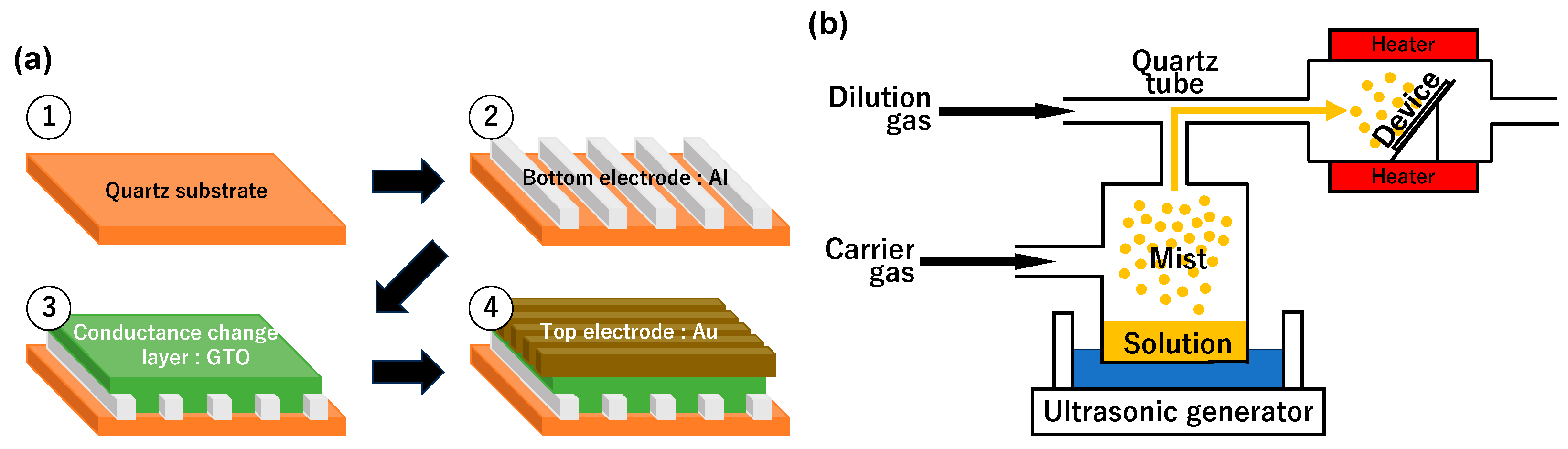
Figure 2.
Memristive characteristic. (a) Hysteresis characteristic. (b) Switching ratio.
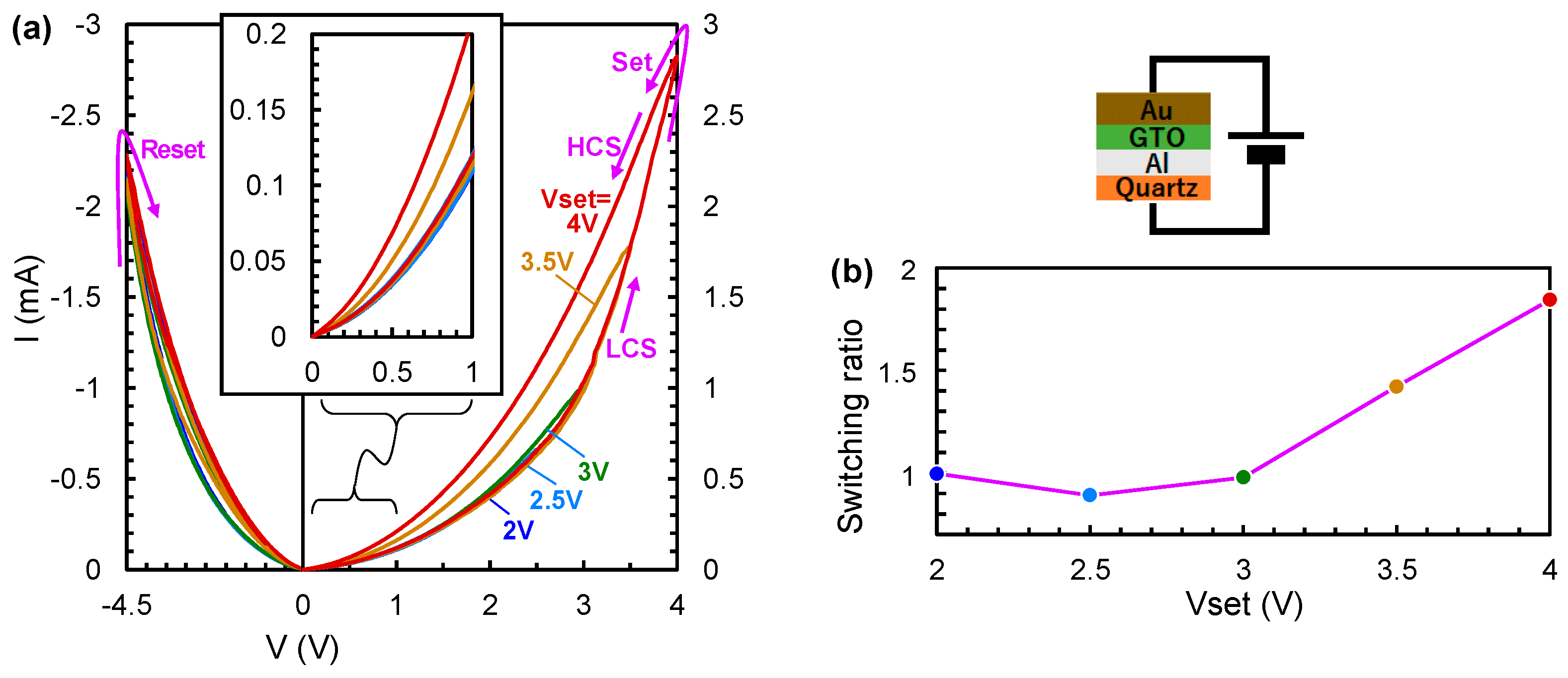
Figure 3.
Spike waveforms. (a) Vpre, Vpost, and Vnet. (b) Vmax.
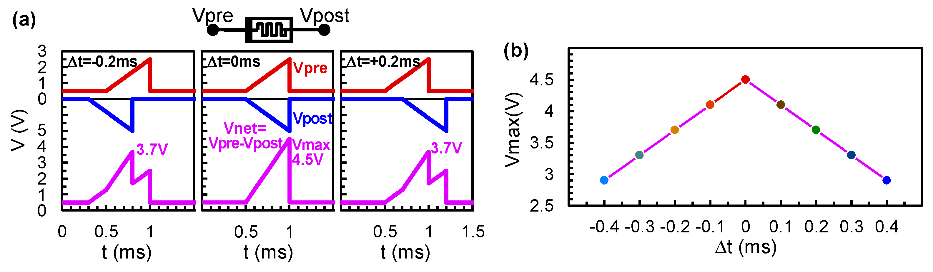
Figure 4.
STDP characteristic. (a) Conductance change along t. (b) Conductance change and switching ratio.
Figure 4.
STDP characteristic. (a) Conductance change along t. (b) Conductance change and switching ratio.
Disclaimer/Publisher’s Note: The statements, opinions and data contained in all publications are solely those of the individual author(s) and contributor(s) and not of MDPI and/or the editor(s). MDPI and/or the editor(s) disclaim responsibility for any injury to people or property resulting from any ideas, methods, instructions or products referred to in the content. |
© 2024 by the authors. Licensee MDPI, Basel, Switzerland. This article is an open access article distributed under the terms and conditions of the Creative Commons Attribution (CC BY) license (http://creativecommons.org/licenses/by/4.0/).
Copyright: This open access article is published under a Creative Commons CC BY 4.0 license, which permit the free download, distribution, and reuse, provided that the author and preprint are cited in any reuse.


