Preprint
Article

Development of Semi Empirical and Machine Learning Models for Photo-Electrochemical Cells

Altmetrics

Downloads

117

Views

56

Comments

0

Submitted:

20 July 2024

Posted:

22 July 2024

You are already at the latest version

Alerts
Abstract
We propose a theoretical Photocurrent - Voltage characteristic (PC-V) model to assess the interfacial phenom-ena for a photo-electrochemical cell (PEC). The origin of voltage deficits and the distribution of the photocur-rent across the semiconductor-electrolyte interface (SEI) are reported for the cell. The model predicts the hole exchange current parameter to extract the cell polarization data at the SEI. The potential drop across the SEI across the cell is mapped for the n-type cells. The simulation results of the Pc-V model are used to differentiate the effect of the bulk and space charge region (SCR) recombination in the semiconductor cells. A deep neural network model is developed to assess the electron-hole transfer mechanism using the Pc-V characteristic curve. The applicability of the model is tested and validated with the real time data. The results show good agreement with the experimental data.
Keywords: 
Subject: Engineering  -   Chemical Engineering

1. Introduction

Hydrogen is a clean energy carrier which can be used to harness heat and power for industrial applications. The use of hydrogen powered fuel cell vehicles (FCV) is increasing by twofold chiefly across the world due to its high efficiency and durability. However, the commercialization of the FCV is limited by high-cost hydrogen production methods such as steam electrolysis, steam and natural gas reforming. The water electrolysis cell shows 70% efficiency, and no green-house gasses are produced in the process. The magnitude of hydrogen produced via electrolysis pathway has increased by twofold since 2010. Thereby, the renewable energy sources (RES) are combined with the water electrolyzer cells to enable energy storage for the microgrids. The electricity obtained from the RES is converted into gas molecules by the cells and stored in the metal hydride wells. This approach can be used as a response management strategy for the smart grids. Although the hydrogen storage systems ensure the stability and security that is needed for the smart grid [1], it is not yet scaled for the local electricity-gas grid requirements. Furthermore, decomposing water to hydrogen molecule using the electrolyzer is still an expensive and energy intensive process. The degradation rate of its components is high when the gas production rates go up during the peak hour electricity energy demand. Deploying cheaper technologies such as photoelectrochemical cell (PEC) will be an alternate approach to produce hydrogen. The cells or stacks can be connected to the 'Power to Gas' grids where hydrogen is injected into the gas-grids and transported to the energy storage infrastructures.
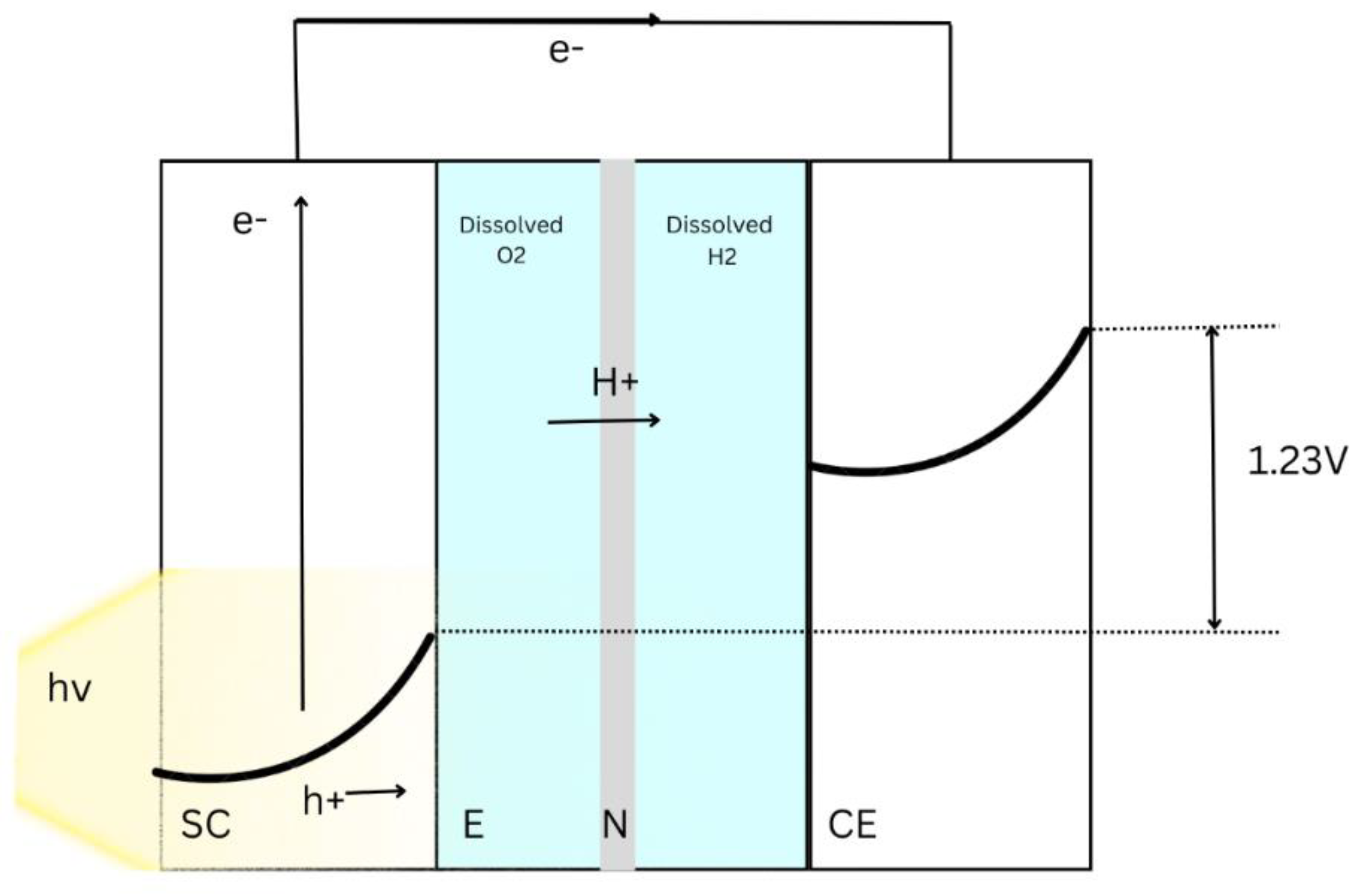
The components of PEC absorb the photons in the sunlight to produce energy. The cell comprises light sensitive nano-materials such as a n or p type semiconductors to absorb photons. Figure 1 depicts the schematic of the cell. The incident photons irradiate the surface of the cell and forms electron-hole pairs at space charge regions. The holes are separated from the electron by the electric field at the surface of the semiconductor. When the electrons depart towards the external circuit, the holes are pushed into the SEI of the cell [2]. In an acidic environment, the electrons flow via the external circuit and reach the interface of the counter electrode (CE). These electrons react with H+ ions and form hydrogen gas at the CE. The holes at the SEI of the photo-electrode react with water to form oxygen species. [2] The reactions steps of the cell are given in Equations 1-2.
4 H + + 4 e 2 H 2             E 0 = 0   V   vs : NHE
2 H 2 O + 4 h + 4 H + + O 2             E 0 = + 1.23   V   vs : NHE
In a basic environment, the holes generated at the semiconductor react with the hydroxyl ions form oxygen while the electrons in the CE decompose water into hydrogen and hydroxyl ions.[2] Equations 3-4 provide the reactions associated with the water splitting.
4 H 2 O + 4 e 2 H 2 + 4 O H             E 0 = - 0 : 828   V   vs : NHE
4 O H + 4 h + 2 H 2 O + O 2             E 0 = 0 : 401 V   vs : NHE
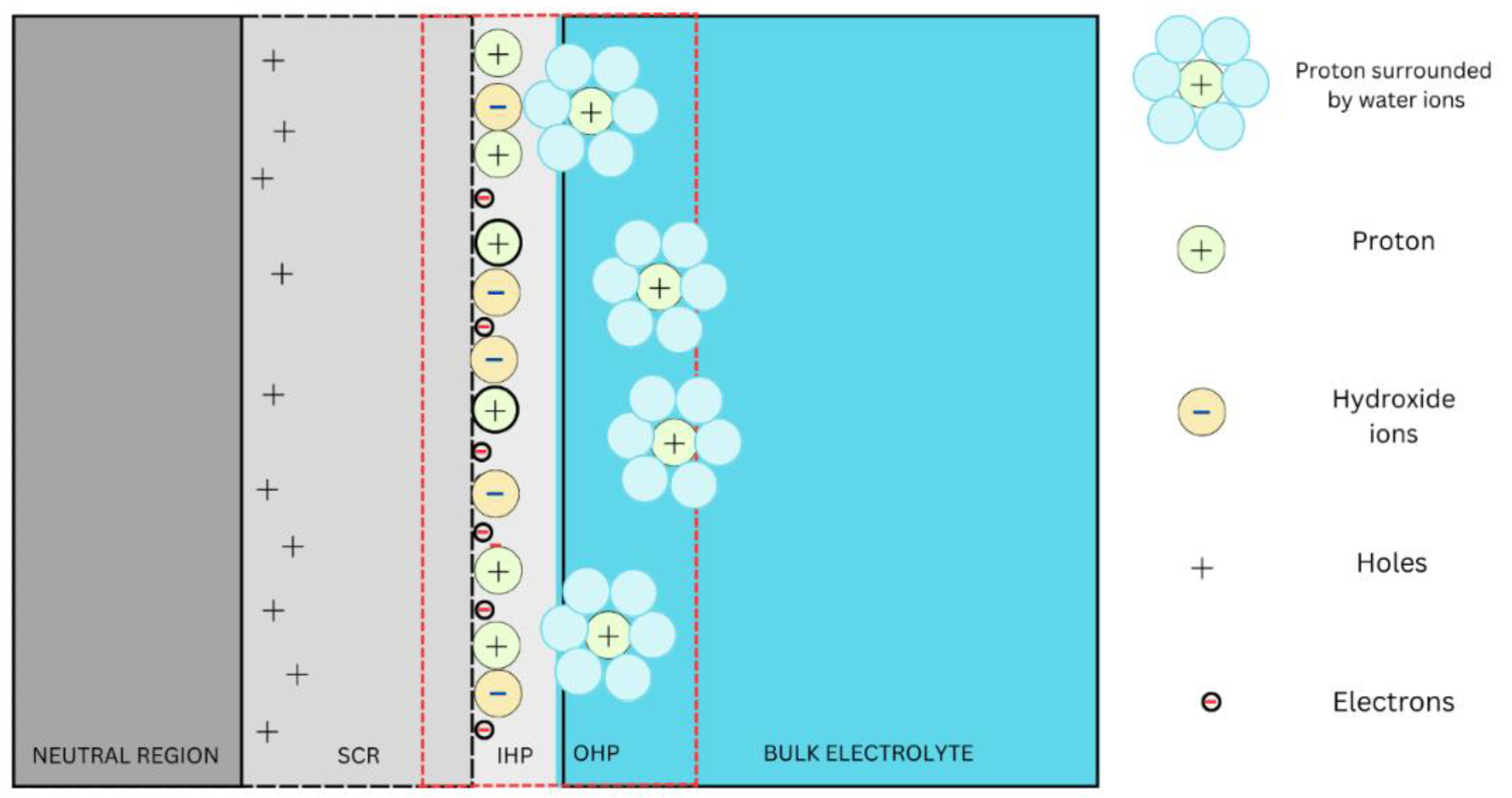
The production rate of the hydrogen from the cell depends on the stability of the Semi-conductor Electrolyte Interface (SEI). It has three regions as illustrated in Figure 2. They are bulk semiconductor, space charge region (SCR) and the Helmholtz regions. The interfacial interactions, mapping of the photocurrent, and the thickness of the SEI against the cell performance are not well understood. The modeling of the layers involves creating an accurate mathematical formulation of the SEI. The mapping of voltage drop across the SEI shall provide an accurate representation on the transport phenomena of the hole-electron pairs and hydrogen production rate. The parameters such as the surface charge width and the size of the band gap are vital in identifying the processing functions, providing the description of the hole-pair and quantifying the rate at which the electrons migrated from the interface to the external circuit. Developing a predictive transport - voltage loss break down model for the SEI is cumbersome as it requires estimation of transport and physicochemical properties of the cell.
Figure 2 provides the schematic of the SEI and highlights the interaction of electrons, donor ions containing holes and the ions in the electrolyte. Empirical models reported in the literature provide description on the role of reverse current, bias, and the recombination parameters at the SEI [3,4]. Any attempt to model the voltage loss break down across the SEI depends on the quality of the photo-current and potential data. The use of large quantities of historical data to create interface models has provided a basis for forecasting, control and optimization. However, the spatial accuracy of the model is compromised as the model has lower dimensionality. Furthermore, describing the semiconductor- electrolytic behavior against the potential loss in the cell is not straight forward. Zero-dimensional (0-D) models reported in the literature identifies relationships between cell components and transport barriers at the semiconductor. Gartner proposed series of theoretical equations to compute the photocurrent generated by the photoelectrode under reverse bias [3]. The performance of the model is limited by the Schottky barrier and the ion transfer across the SEI. The model could not address issues related to the recombination at the SEI. Reichman improved the 0-D model and provided equations to compute the potential drop across the bulk and SCR recombination regions at the SEI [4] Equation 5-7 are used by Reichman to calculate the current due to minority carriers, Jp.
J p = J g J o e q V k T ( 1 + J o e q V k T I p o )
J o = q p o L p ζ
p o = n i 2 N d
where n i is the intrinsic carrier density(m -3), N d is the carrier density (m -3), J g corresponds to Current Density in the Gartner model(A m-2), q corresponds to elementary charge(C), I0 is the photon flux,(A-m-2) I n o and I p o are the electron and hole exchange current parameters(A m-2), W is the space charge width(m), L p is the hole diffusion length(m), α is the optical absorption coefficient of the semiconductor(m -1), J o is the saturation current density(A m-2) and ζ is the hole lifetime(sec).
Unlike 0-D models, one-dimensional (1-D) models represent the PEC system in a single axis. Wenger et al [5] report 1-D models for the Dye sensitized cells (DSC) where the optical and electrical equations are coupled [5]. Their model captures the behavior of the DSC and provide an accurate description on how the excited electrons convert the incident photons to electricity [6]. In a DSC, the photo-sensitive dye is injected into a wide-bandgap semiconductor to harness the photocurrent. Therefore, the dye absorption rate, an output of the optical model, is trivial to obtain the steady state dye electron injection efficiency and hole diffusion length. [5]. The balance between complexity and computational efficiency is hard to achieve in both 0-D and 1-D PEC models. Hence, Two-dimensional models are reported by Hernandez et al [7]. They analyze the oxygen bubbles covering the electrode in the PEC by approximating the inner surface layer as a two-dimensional flat surface. Giacoppo et al reported three dimensional models to provide an accurate representation of the PEC system but the convergence of their model is limited by computational complexity [8]. Their model is formulated based on the Gartner’s equations. The simulation of the 3D model shows that the cell attained 10 mA cm-2 at bias voltages of 1V. But no recombination losses are accounted in their model. Although modelling of DSCs and microscopic interfacial behavior in the PEC have been studied extensively, focused efforts on modelling of the SEI and probing the recombination mechanism for the PEC nano-materials is still not explored well. 0-D models developed by the Reichman (Equations 5-7) show a good approximation of the experimental polarization plots. They report that the recombination in the SCR and charge transfer across the SEI depends on the current exchange parameters. They are determined by (a) the degree of overlap in the semiconductor band, (b) interface states with the redox ions and (c) the transition probabilities for charge transfer [4]. The values of the exchange current parameters for n or p-type materials are not readily available to scale their model for new photoelectrode nano scale materials. No attempts are made to estimate the current exchange parameters for the photoelectrode nanomaterials.
The decisions on the operating strategies of the PEC are attained by combining the physical computations of the theoretical models with experimental data. Simplified Semi empirical models reported in the literature adopts linear regression where corelation amongst variables are achieved. This approach cannot be directly used to diagnose the cause-effect-mechanism of the PEC’s components. Increasing amounts of data generated from the cell are not effectively used to assess the durability, and performance of the cell. A model that can (a) reveal the electrochemical parameters; (b) classify large number of the materials properties to reinforce the learning; (c) perform iterative tasks through repeated interactions with the i-V dataset in a dynamic environment; (d) explore huge i-V data sets to identify the features and pattern in the PEC electrodes would be useful to set the design metrics for the next generation cell. Uncovering the hidden pattern or feature in the i-V dataset will provide new strategies and operating protocols for the PEC. However, no such model is readily available in the literature. Even modern quantum chemistry methods are not accurate to predict the complex characteristics such as diurnal variation of the cell. The machine learning models could resolve the listed research needs. Applying the ML models could address the performance decay related to the diurnal variation. Furthermore, structure – property – performance relationship can be attained for the cell using the ML models. Integrating the experimental data with ML techniques will be useful to uncover the operating and the failure modes of the cell. It could provide a common pattern, specific predicted electrochemical properties, and strategies for the real world testing of the cell.
Predictive maintenance of the PEC depends on the durability and the PC-V datasets. The machine and deep learning models are needed to understand the non-linearity in the PC-V data collected from the cell. The architecture of the deep learning models can process wide range of datasets and accurately predict the PC-V characteristics than the traditional machine learning or 0-D models. It has the ability to ingest and process the given datasets via several iterations and learn the non-linearity in the features. Developing algorithms, reducing the computation power, and creating a database of the PEC parameters could provide enormous growth in applying Deep Learning in Simulation (DLS) for the cell. It can handle noise in the data and make efficient predictions based on the history of the data collection. The complex trends between photocurrent, voltage and important intrinsic parameters in PECs can be captured using the DLS approach for different nano-materials. Wang et al [9] built a machine learning model to predict the effect of dopants on photoelectrodes.[9] Oral et al [10] implemented Random Forest, Decision tree and Association Rule Mining to predict bandgap and photocurrent density. They have used thirty-three features including electrode materials, methods of synthesis, irradiation properties and electrolyte in their model [10]. Kharade et al reports an Artificial Neural Network (ANN) model that predicts the adsorption efficiency in a DSC using a three-layer approach for a DSC [11]. The parameters such as Fill factor, short circuit current and open circuit voltage are considered in the model optimization and the efficiency calculations. Despite having ML models for predicting photocurrent using features and voltage datasets, they still need high computational power and time. A model with robust algorithm is required to capture the real time events of the cell and circumvent the numerically intense calculations of 0-D modelling A framework comprising of a 0-dimensional model coupled with the DLS algorithm can be useful to accelerate the new material development for the PECs.
Based on the current state of research, the present work pursues the following objectives; (a) Derive a theoretical model to assess the current density across the SEI for two different PEC components. The model shall; (b) approximate the hole exchange current parameter (Ipo); (c) evaluate the photocurrent across the SEI; (d) demonstrate voltage loss break down against the cell parameters for the gallium arsenide and pristine silicon cells, and (e) develop an ANN model to predict photocurrent for the cell; For the first time, we aim to provide a framework that consists of an analytical model and machine learning model that can provide parameters such as space charge width and the photocurrent.

2. Materials and Methods

Section 2.1 focuses on formulating equations for the PC-V model. A derivation to estimate the hole current parameter and the photocurrent density across the SEI is presented. Section 2.2 focuses on developing an ANN-based DLS model to predict the photocurrent density across the SEI.

2.1. PC-V Model

The voltage loss in the cell depends on the stability of the band gap, number of photons collected by the semiconductor, recombination occurring in the photoelectrode, and the performance of the individual cell components. The photo-oxidation of the electrode materials and their reaction with water molecules is limited by the presence of the surface-trapped holes at the surface. The voltage loss in the cell is contributed by the rate anodic decomposition and cathodic photo-reduction reactions. Understanding the role of the layers in the SEI such as SCR, inner and outer Helmholtz layers is the first step in identifying the voltage loss contributors. The SCR is the first region in the SEI where the electric fields are formed by the electrons in the semiconductor and the ions in the bulk regions. The optimization of the SCR width and the electric charge in this region is significant to improve overall efficiency of the cell. The region formed between the ions (protons and hydroxide ions) adsorbed in the semiconductor and the solvated ions in the electrolyte is called the Helmholtz region. The adsorption and desorption of protons and hydroxide ions occurs continuously at the interface. The polarization of the SEI depends on the thickness of these three SEI-layers [12]. Two main drivers for the photocurrent generation are the width of the space-charge-recombination and the distance between inner and the outer Helmholtz layers. If the lattice structure of the photoelectrode is abnormally terminated or not optimized, electronic states will be formed within its bandgap. These states are filled with the electrons supplied from the bulk region of the semiconductor. The ions originated from the bulk free electrons regions create positive space charge regions [2]. Poisson’s law is used to model the charge in the SCR and the space charge width. It correlates the potential and the net amount of charge produced at the interface. The width of the SCR is computed according to the equation 6.
W = 2 ϵ r ϵ 0 V k T q q N d
where W is the width of the SCR(m), ϵ r is the relative permittivity of the semiconductor material(unitless), ϵ 0 is the electric constant, V is the voltage across the SCR(V), k is the Boltzmann Constant(JK-1), e is the elementary charge(C), T is the temperature(K).
The charge accumulated in the SCR is computed using Equation 7.
Q S C = 2 ϵ r ϵ 0 e N d A 2 V k T q
where A is the surface area of the semiconductor(m2).
The pH-value at which the net adsorbed charge is zero is termed as the Point of Zero Charge (PZC). In this region, both the inner and the outer Helmholtz layer have adsorbed and solvated ions respectively, at the electrolyte surface (Figure 2). The potential drop across the Helmholtz region is calculated according to the equation 8
V H = 2.3 k T q P Z C p H
where V H is the Helmholtz potential. The charge and the width of the SCR varies if dopants are used in the photoelectrodes. The carrier concentrations of doped species are obtained from [13]. The voltage drops across a TiO2 doped semiconductor is evaluated using the value of PZC as 5.6 provided elsewhere [14]. The assumptions employed in the derived model are ; (a) The charge transfer across the SEI due to the holes and electrons generates electric current; (b) The current density across the SEI is function of the exchange current parameter; (c) The ratio of concentration of holes and electrons across the interface is calculated based on the following assumptions (cf. [3]); (d) The width of the Helmholtz layer is small; (e)The voltage across the Helmholtz layer is constant; (f) Ion concentrations at the interface are constant; (g) No mass transfer effect is considered; (h) No concentration polarization is accounted; and(i) Charge transfer reactions are first order with respect to minority and majority carriers at the interface.
The current density due to holes (Jp) is substituted with the total current density from the performance curves during calculation in the semi empirical formula for the hole exchange current parameter as isolating values of Jp requires highly sophisticated equipment.
The current density due to minority carriers(holes) [4] is computed using the Equation 9
J p = I p o p s p s o 1
where J p is the current density driven by holes(A m-2), p s is the hole concentration at the interface (m -3) and p s o is the equilibrium hole concentration at the interface. (m -3). The hole carrier density across the interface is obtained by solving the diffusion equation for minority carriers in the neutral region of the semiconductor
D d 2 p d x 2 p p o ς + I o α e α x = 0
where D is the diffusion coefficient (m2s-1, ς is the hole lifetime(s), p o is the equilibrium hole density(m -3), I o is the monochromatic photon flux (A m-2) incident at the semi-conductor after loss corrections. The correction factor includes interface reflections and electrolyte absorption, and α is the optical absorption coefficient (m -1). The first term in Equation 10 represents the change in the hole density across the x axis inside the semiconductor. The density depends on the diffusion of holes at the semiconductor surface. The second term recombination of holes driven by the completion of their lifetimes. The third term represents the formation of new holes due to incident monochromatic photon flux.
Jg=Jo+qIo1eαW1+αLp
The SCR width can be approximated using Equation 12
W = 2 ϵ r ϵ o ϕ b q N d
where ϕ b = ϕ b 0 -V, where ϕ b 0 is the flat-band potential of the semiconductor and V is the Voltage across the SCR. The current density due to electron flow is given in Equation 13. The Reichman model (Equation 5) considers the increasing rates of recombination in the neutral region and neglects the recombination effect in the SCR and the interface. The equation 5 and 13 describes the hole carrier current density (Equation 5) and the current density measured due to flow of electrons respectively (Equation 13). By combining these two equations, the polarization plot for neutral recombination regions can be obtained.
J n = I n o e q V k T 1
The recombination current is expressed using K and the ratio of hole concentration and the equilibrium hole concentration at the SEI. Reichman studied the recombination in the SCR using a method proposed by Sah et al. [15] According to their model, the recombination current depends on the parameters A, B and K. Equation 14-18 summaries the modified method adopted in this study based on [4 and 15].
J S C R R = K p s p s o
A = I p o + J o e q V k T
p s p s 0 = K + K 2 + 4 A B 2 A 2
B = I p o + J g
K = π k T n i W e q V 2 k T
where J S C R R is the recombination current (A m-2), T is the temperature of operation(K) and W is the SCR width (m) (Equation 12). Since no hole exchange current parameter values I p o are available for the PEC components, we derive an analytical expression to estimate the I p o by solving equations 9 and 16. The assumptions considered in the derivation are given below. I p o >>   J o e q V k T
J g > > I p o I p o > > z
The current exchange parameter values observed so far in literature present themselves in values far less than the current density according to the Gartner model( J g ) and more than the saturation current density with the multiplied exponential as in the first assumption. The values of the hole exchange current parameter generated for every point in the J-V curves that satisfy all the assumptions are selected for further analysis in the model. These considerations justify the assumptions taken in the model. The datapoints from performance curves, yielding total photocurrent density, are used to calculate the value of I p o at all instances as isolating the values of hole current density requires highly sophisticated equipment. The mean of all I p o values satisfying all the above assumptions is further used for further calculation using Equations 5 and 13. The derivation for the hole exchange current parameter, I p o (Equation 19) is provided in the appendix.
I p o = K J g + J g K 2 + 8 ( J p J g ) K 2 4 J p J g

2.2. DLS Model

DLS approach is used to predict the photocurrent as it reduces the complexity in numerical calculations and provide the IV curve for the PEC. It needs an Artificial Neural Network (ANN) algorithm which includes the data extraction, data cleaning and pre-processing. The data used for training the model is obtained from [16]. The klib library is employed to expunge and clean the data and assess its data quality. Repeated rows and empty columns are dropped in the data cleaning process. It reduces dimensionality and the memory required for further processing. We used Standard Scalar method to normalize the datapoints. The treated datasets are normalized to enable the faster convergence. This is achieved by assessing the values of features to a common scale and an algorithm is developed that is less sensitive to the feature sizes. The model used to treat the dataset is given in Equation 20.
Z = X μ σ
The normalized dataset is split into training and testing sets in an 80-20 ratio before invoking the regressor for training the model. The regressor is initialized with the number of nodes, type of kernel initializer and activation functions. The ANN model used in DLS is given in Equation 21.
y = f w 1 x 1 + w 2 x 2 + w 3 x 3 + . . . + . . w n x n + b
where x1, x2, ..., xn represent the inputs to the ANN model, w1, w2, ..., wn are the corresponding weights for each input, b represents the bias term, and f represents the activation function. The perceptron algorithm applies a weighted sum to the given inputs and a bias term is added. It passes the result through an activation function to produce an output.
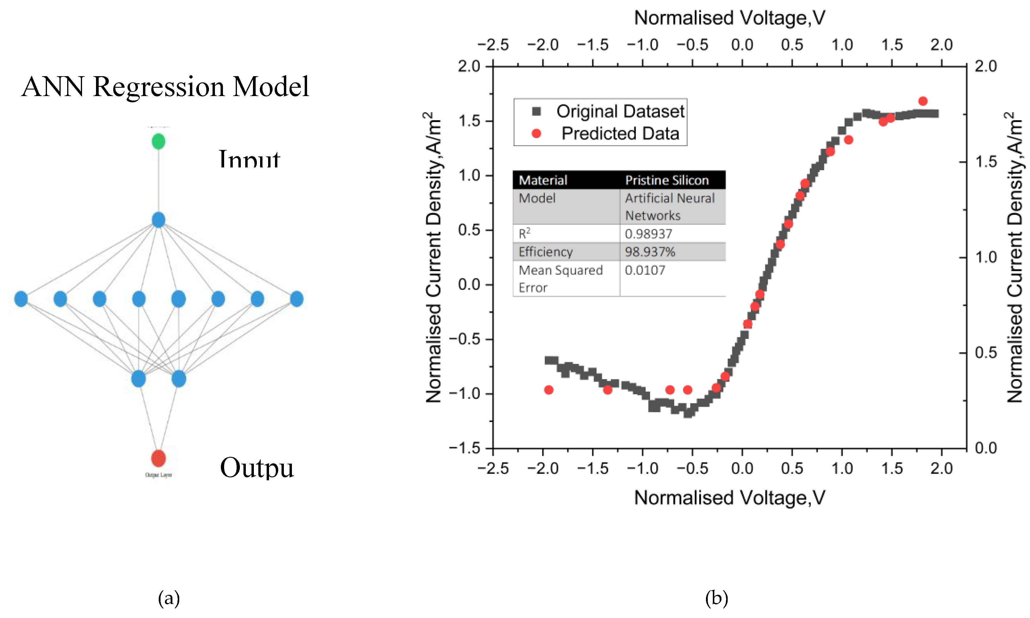
The ANN model used for this research contains 2 hidden layers with 8 and 2 nodes in the first and second hidden layers, respectively. Random uniform, the kernel initializer used for the model in this research ensures that the weights are initialized with a uniform range of values, which prevents vanishing or exploding gradients during model training. If the neurons are initialized with weights having very small or large values, it makes it difficult for the network to learn and update the weights properly, thus yielding a poor performance. Every neuron works in cohesion with a weight initialized by the initializer, a bias value and the activation function. Rectified linear function (ReL) is used as the activation function for the ANN model. The ReL, is piecewise linear function that ensures the qualities of linear regression. A stochastic gradient descent model (Adam) based on the adaptive estimations of lower order moments is used [19]. It calculates the error between the predicted and the training data and adjusts the values of the bias and the weight in the neurons to increase the model’s efficiency. The regressor is used to predict the output features based on the training dataset and the efficiency of the model is calculated. Mean squared error is the metric used for error estimation and model validation.

3. Results and Discussions

3.1. PC-V Model

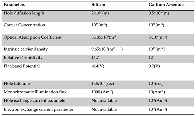
Although PC-V experimental plots for several semiconductor material is widely recorded, quantifying the voltage loss contributed by the oxidation half-reaction on metal oxide surfaces poses challenges to predict current-voltage characteristics for the cathodic and anodic reactions. Empirical model requires I p o to compute the PC-V simulation. The datapoints from experimental characteristics and the yielding-photocurrent density are used to calculate the value of I p o for all materials assessed in this study. Since isolating the values of hole current density is not straight-forward, the mean of all I p o values calculated from the total current density is taken. Table 1 lists the values for the parameters used in the model [4,16,17,18]. Solving Equations 5 and 13 provides the magnitude of the photocurrent generated due to migration of holes across the interface, and the electron migration, respectively. The total photocurrent across the SEI is computed by summing the individual photocurrent densities evaluated from the equations. The hole current density across the SEI is compared with the experimental performance curve of pristine silicon to identify and validate trends between them.
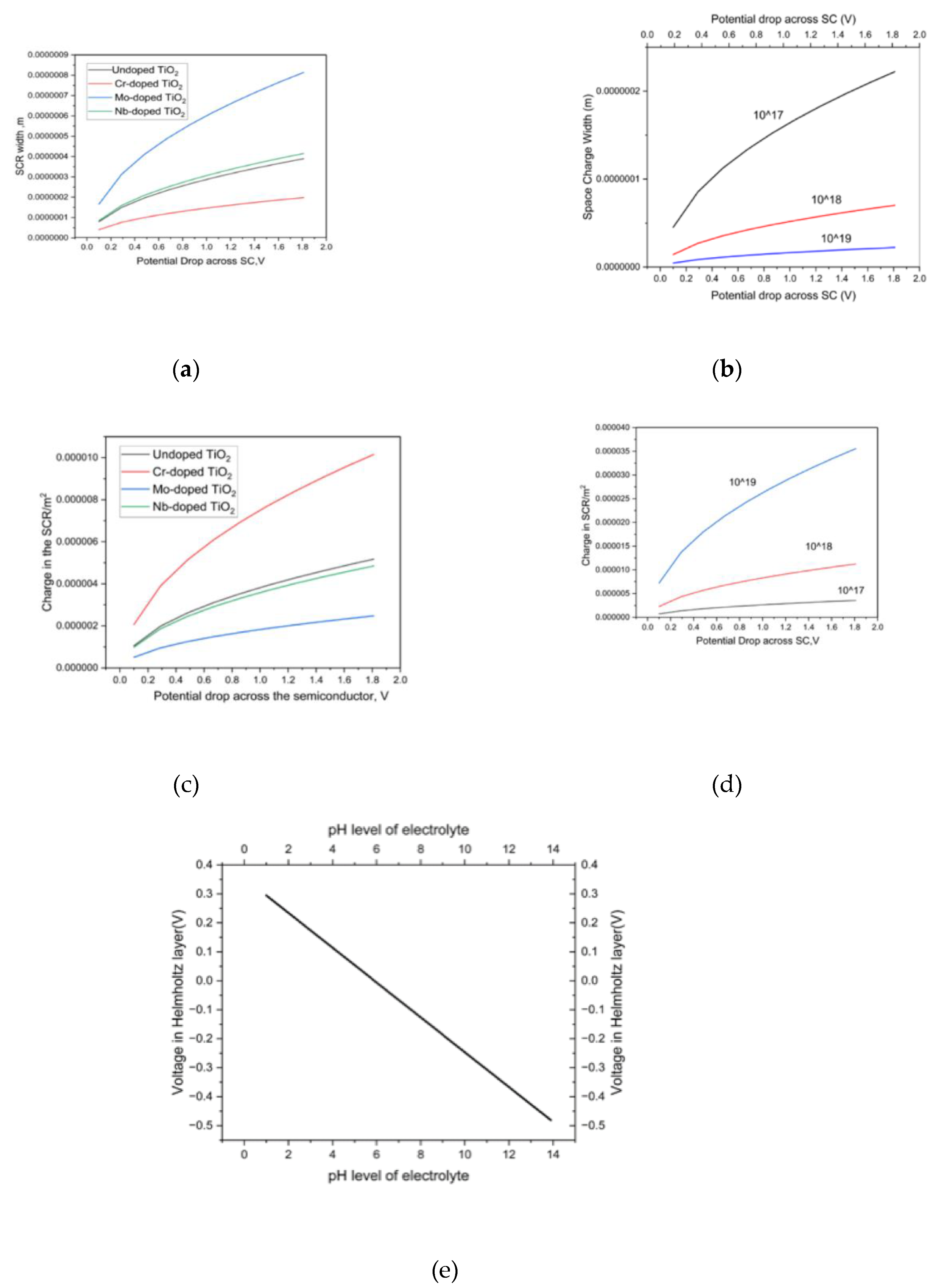
The variation of SCR width against the potential drop across the SEI between TiO2 with different dopants is plotted in Figure 3a. The SCR width of Mo-doped TiO2 is widest among the dopants while Cr-doped TiO2 has the lowest SCR width. The availability of excess valence electrons in the case of Cr-doped TiO2 increases the carrier density, leading to an increase in charge and width of the SCR. The reduced electron availability in the case of Mo-doped TiO2, leads to a weaker electric field, thus provides larger SCR width. Figure 3b shows the variation in space charge width of hematite with changes in carrier concentration. The carrier density depends on the dopant and the amount of doping performed. Therefore, doping level is a deciding parameter in determining the SCR width. Transfer of free electrons from the bulk is the other factor that determines the formation of the SCR. Any increase in the carrier density results a dramatic increase in the charge in the SCR (Figure 3c-d). The charges in the SCR and the width of the SCR show an inverse relation with each other. The changes in voltage across the Helmholtz layer as a function of the pH-value of the electrolyte for anatase TiO2 is analyzed in Figure 3e. A positive to negative shift in voltage is observed when the pH reaches 5.9. The shift in Helmholtz layer voltage occurs due to the decreasing number of protons (or increasing amounts of hydroxide ions) with increasing pH and the number of electrons available at the surface states of the semiconductor. An increase in pH leads to a subsequent increase in hydroxide ion concentration (or reduction in proton concentration) in the electrolyte. The increased concentration causes more adsorption of hydroxide ions than protons, causing a reversal of Helmholtz voltage.
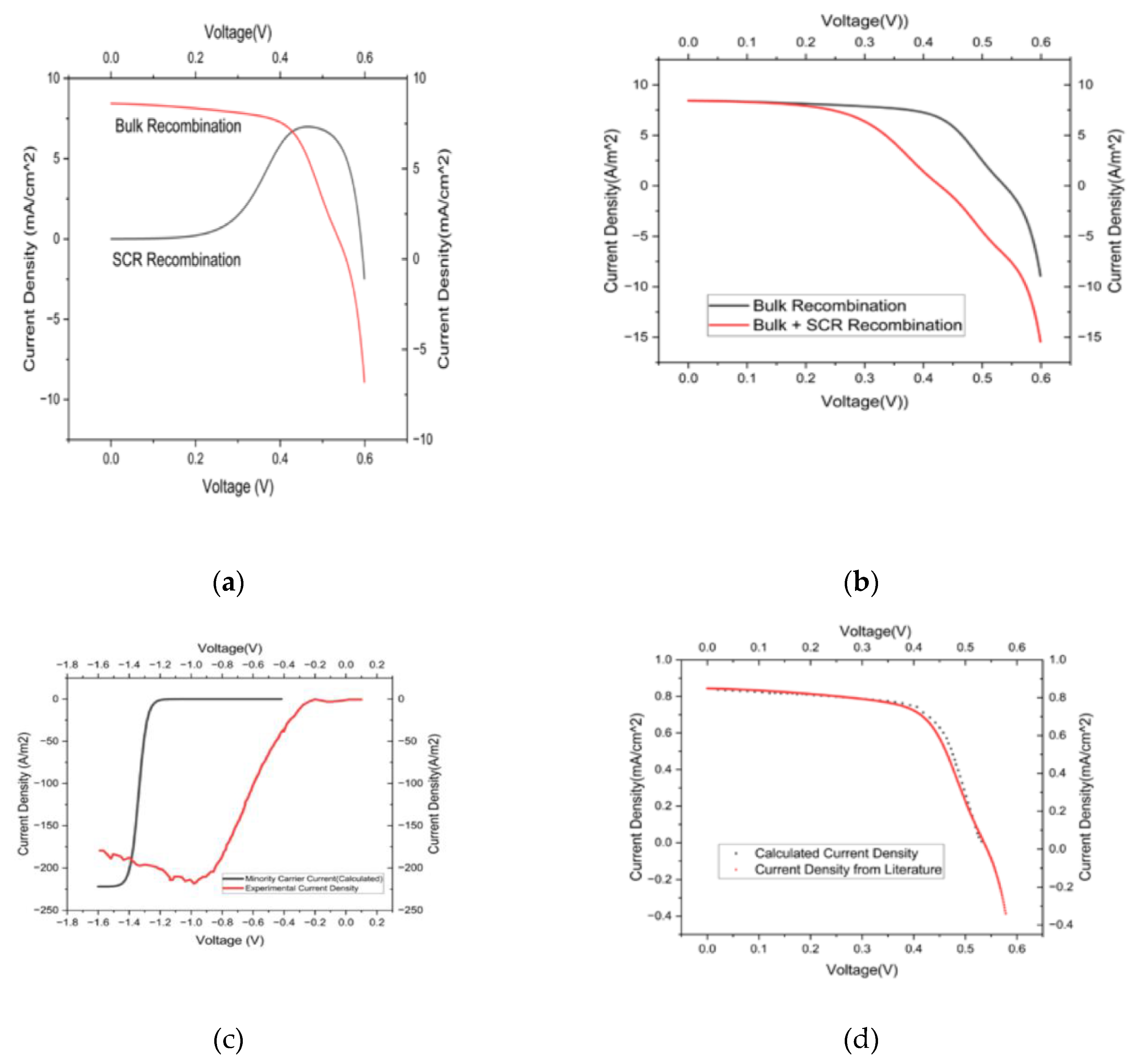
The performance of the cell is given in Figure 4. The details related to the energy conversion efficiency as a function of applied potential, sign of the photocurrent (anodic or cathodic), onset potential, the limitation related to the electron/hole-transport, and the transient effects can be inferred using the cell performance data. The changes observed in photo-current density, after accounting for bulk recombination and the recombination current, is plotted against voltage in Figure 4a. The model prediction is validated with the data collected from the literature.[4]. Reichman equation does not emphasize the recombination current separately but the 0-D model proposed in this study can provide the loss contributed by the recombination effect. We observe that the current density is decreasing due to increase in bulk recombination, it is inferred by following the decreasing voltage trend in the characteristic curve. The onset of bulk recombination is observed at 0.4V. SCR recombination current starts rising from 0.3V and reaches maximum near 0.45V. The values of low diffusion coefficient and the defects in the semiconductor lead to bulk recombination. It hinders the flow of carriers between the electrodes and SEI. The minority carrier is building upat the SEI due to the rate limiting effect and affects interface charge at higher voltage regions [2]. The total current density across the SEI obtained by summing the SCR and bulk recombination currents is given in Figure 4b. The effect of SCR recombination is more pronounced at higher voltage regions where the SCR recombination current opposes the generation of the photocurrent. The effect of SCR is consistent with the similar observations reported in Figure 4a. At 0.4V, we observe an 80.78% reduction in the photocurrent density between the effects of bulk and the combined effects of bulk and SCR recombination. It is caused by the reduction in SCR width, consequently causing the holes and electrons to come close together, leading to a higher probability of recombination in the SCR region.
The hole exchange current parameter values calculated for silicon and gallium arsenide using the analytical expression (Equation 19) are mentioned in Figure 4. Similar trend is observed between the experimental and modelled hole current density date for pristine silicon (Figure 4(c)). The hole current density flattens at -1.2V. The electron flow across the SEI after -1.2V influences the photocurrent generation. Addition of electron and hole current densities increases the photocurrent density across the SEI due to illumination. Furthermore, the model prediction in this region can be limited by varying real time input parameters such as the quantifying the solar spectrum at the semiconductor surface, dispersion of the catalyst particles at the photoelectrodes and the bandgaps of the materials used, these parameters determines the photogenerated holes. Transporting holes, electrons, and optimizing the SEI shall boost the overpotential of the cell. Capturing these phenomena using a 0-D model is not easy. Figure 4(d) compares the polarization curve across the SEI for gallium arsenide calculated using the hole exchange current parameter’s analytical expression with the polarization curve from the literature. The experimental data are in good agreement with the model polarization curve data (R2 = 0.997). The bias voltage applied to the n or p type semiconductor determines the solar-to-hydrogen efficiency and the difference in model prediction. Small overpotentials are adequate for hydrogen evolution in n-type photoelectrodes whereas the HER is effective when overpotentials are high at the p-type photoelectrodes. It is difficult to formulate these items in the 0-D model. Therefore, figure 4 c and 4d are not directly comparable.

3.2. DLS Model

A visual representation of the ANN model with the input, output and hidden layers is depicted in Figure 5a. It simplifies the visualization of the flow of the input feature through the network of neurons and helps understanding the complex network of neurons present in the ANN model. The efficiency and R2 value of the model is 98.937% and 0.98937, respectively. A mean squared error of 0.0107 is observed. Figure 5b shows a comparison between the actual and predicted data for a change in normalized photocurrent density with normalized voltage. The predicted data closely corresponds to the trend of the original dataset with a slight deviation at low voltage. The low mean squared error value is a clear indication that the model is able to capture the complex relationship between the parameters in the dataset and thus is an excellent fit for the data.

4. Limitations and Applicability of the Semi Empirical and ANN Models

The empirical model presented in this study adopts a common derivative methodology based on Gartner et al. A direct correlation between Space charge width, I p o and voltage for materials such as gallium arsenide and pristine silicon in a PEC system is established. This exercise is not a straight-forward approach as it was impossible to obtain a correlation between hole exchange current parameter and current in a mathematical model. The framework uses regression approach to solve the model and captures all experimental measured data points. However, the accuracy of the prediction of voltage or current drop relies on the extrapolation attempt and error minimization methods. The fundamentals transport mechanisms underlying the Solid electrolyte interface is considered for the first time and correlated to obtain specific parameters. Therefore, it is extremely useful to improvise Gartner’s model when a framework unable to identify or differentiate I p o to perform the analysis. The trend of the experimental data has accurately predicted the behavior of the PEC. However, the model derivation and approach are lengthy. Since the number of variables are more and data analysis methods presented here in cumbersome, the model could yield unpredictable results when the size of the experimental data file is large. To overcome this issue datamining is needed to make universal format to present the data obtained from the model and the experiments. Predictability of the empirical model predict is severely limited by the a particular operating range or initial designed of experiment carried out by the observer. However, the model can be directly used to calibrate and predict of preliminary experimental data in the PEC.
We have used the Artificial neural network (ANN) toolbox models to improve the prediction and assess the efficacy of the empirical model although this approach requires large experimental database at specific operating condition. Using the database, the polarization patterns are recognized in the big dataset. The ANN model consists of an interconnected collection of artificial neurons and connected input/output parameters where each of the connection has been associated with the weight. It involves long training times because we have several parameters involved in the hydrogen conversion process. Furthermore, these parameters are determined empirically in this study. The advantage of the proposed ANN model is (a)its ability to handle many tasks at the same time (b) its predictability improved by number of cells and networks (c) ability to function even if neural network gradually broken down (d) its functionality to learn from past events to make right decisions. However, solving the ANN model and performing datamining are computational expensive.

5. Conclusions

We report a semi-empirical and deep learning simulation model to assess the performance of a PEC. The PC-V model accurately computes the photocurrent density for n and p type semiconductor nano scaled materials using the modified equation provided in this study. Hence, the performance of the cell as a function of voltage that was difficult to assess so far, can be accurately computed. The polarization curves for two different nano materials, gallium arsenide and pristine silicon were calculated with a R2 value of 0.997(GaAs) between the calculated curve and the curve found in literature. The ANN model predicts the photocurrent values with voltage as the input feature with an efficiency of 98.937% and a mean squared error of 0.0107. The polarization analysis and performance prediction pave the way for model-assisted analysis and optimization of the SEI in PECs. The present model can be extended to the analytical approximation for the electron exchange current parameter and calculate the electron’s contribution to the current density across the SEI. Nevertheless, the model as presented here is a valuable tool in assessing the performance across the SEI, identifying loss channels and optimizing the interface parameters for the highest efficiency.

Author Contributions

Conceptualization, SRD., CRK. and N.S; methodology, N.S; SRD; software, C.R.K; validation, S.R.D; M.F., M.S., and B.W; and D.S.; formal analysis, N.S and C.R.K.; investigation, M.F., S.R.D, D.S;; resources, S.R.D,.; data curation, N.S.; writing—original draft preparation, S.R.D and N S.; writing—review and editing, B.W, S.R.D and M.S.; visualization, S.R.D and N.S.,; supervision, S.R.D.; project administration, M.W; S.R.D, and B.W;.; All authors have read and agreed to the published version of the manuscript.
Funding

No funding received for this work.

Data Availability Statement

Raw data is unavailable due to confidentiality.

Acknowledgments

The authors would like acknowledge the Crackow university of technology, Poland for paying the article processing charges.

Conflicts of Interest

No conflict of interest is reported.

Appendix A

The hole exchange current parameter is derived using the following equations. (Equations A.1-A.5)
A = I p o + J o e q V k T
p s p s 0 = K + K 2 + 4 A B 2 A 2
B = I p o + J g
K = Π k T n i W e q V 2 k T
J p = I p o p s p s o 1
Assuming I p o >>   J o e q V k T and J g >> I p o , the parameters A and B are reduced to simpler expressions. (Equation A.6)
A = I p o   and   B = J g
On Substituting p s p s 0 , A and B and from equations A.2 and A.6 respectively in Equation A.5, we obtain the following expression on simplification. (Equation A.7)
J p = 2 K 2 2 K K 2 + 4 I p o J g + 4 I p o J g 4 I p o 2 4 I p o
J p = K 2 2 I p o K K 2 + I p o J g 2 I p o + J g I p o
We can further simplify the expression by extracting K from the component under the square root of the expression. (Equation A.9)
J p = K 2 2 I p o K K 2 + I p o J g K + J g I p o
The terms J g and J p both represent current across the SEI and thus have been brought to the same side of the equation. (Equation A.10)
J p J g = K 2 I p o K J g K 2 J g + I p o I p o
K 2 J g is assumed to be equal to a new term z to simplify the expression. (Equation A.11)
J p J g = K 2 I p o K J g z + I p o I p o
2 ( J p J g ) is substituted with a new term m to obtain Equation 24.
m = K K J g z + I p o 2 I p o 2 I p o
I p o = K K J g z + I p o 2 I p o 2 m
Assuming I p o >>z, Equation A.13 is re-written as:( Equation A.14)
I p o = K 2 m K m J g I p o 2 K m I p o 2
m I p o = K 2 K J g I p o 2 K I p o 2
Assuming I p o as x,
2 K x 4 + m x 2 + K J g x K 2 = 0
Since I p o is a very small number, I p o 2 << I p o which implies that x4 << x2. Thus the fourth order term of the equation is neglected to obtain a quadratic equation.
m x 2 + K J g x K 2 = 0
The root of the quadratic equation has been calculated and the negative root has been neglected.
The final expression for the hole exchange current parameter is as follows. (Equation A.18)
I p o = K J g + J g K 2 + 8 ( J p J g ) K 2 4 J p J g
The above expression (Equation A.18) is the derived analytical equation for the hole exchange current parameter.

References

  1. IEA (2021), Global Energy Review 2, IEA, Paris https://www.iea.org/reports/global-energy-review-2021, (2021).
  2. de, K. R. van, & Grätzel Michael. Photoelectrochemical hydrogen production. Springer. (2014).
  3. W.W. Gartner, Phys. Rev. 116, 84 (1959).
  4. Reichman, J.: The current–voltage characteristics of semiconductor-electrolyte junction photo-voltaic cells. Appl. Phys. Lett. 36, 574–577 (1980).
  5. Wenger, S., Schmid, M., Rothenberger, G., Gentsch, A., Grätzel, M., & Schumacher, J. O. (2011). Coupled Optical and Electronic Modelling of Dye-Sensitized Solar Cells for Steady-State Parameter Extraction. The Journal of Physical Chemistry C, 115(20), 10218–10229. [CrossRef]
  6. Sharma, K., Sharma, V. & Sharma, S.S. Dye-Sensitized Solar Cells: Fundamentals and Current Status. Nanoscale Res Lett 13, 381 (2018). [CrossRef]
  7. Hernández, S., Barbero, G., Saracco, G., & Alexe-Ionescu, A. L. Considerations on Oxygen Bubble Formation and Evolution on BiVO4Porous Anodes Used in Water Splitting Photoelectrochemical Cells. In The Journal of Physical Chemistry C (Vol. 119, Issue 18, pp. 9916–9925). American Chemical Society (ACS), (2015). [CrossRef]
  8. Giacoppo, G.; Trocino, S.; Lo Vecchio, C.; Baglio, V.; Díez-García, M.I.; Aricò, A.S.; Barbera, O. Numerical 3D Model of a Novel Photoelectrolysis Tandem Cell with Solid Electrolyte for Green Hydrogen Production. Energies 2023, 16, (1953). [CrossRef]
  9. Wang, Z., Gu, Y., Zheng, L., Hou, J., Zheng, H., Sun, S., & Wang, L. Machine Learning Guided Dopant Selection for Metal Oxide-Based Photoelectrochemical Water Splitting: The Case Study of Fe 2 O 3 and CuO. In Advanced Materials (Vol. 34, Issue 10). Wiley, (2022).
  10. Oral, B., Can, E., & Yildirim, R. Analysis of photoelectrochemical water splitting using machine learning. In International Journal of Hydrogen Energy (Vol. 47, Issue 45, pp. 19633–19654). Elsevier BV, (2022). [CrossRef]
  11. Kharade, S. K., Kamat, R. K., & Kharade, K. G. Simulation of Dye Synthesized Solar Cell using Artificial Neural Network. In International Journal of Engineering and Advanced Technology (Vol. 9, Issue 2, pp. 1316–1322). Blue Eyes Intelligence Engineering and Sciences Engineering and Sciences Publication – BEIESP, (2019).
  12. Konorov, P. P., Yafyasov, A. M., & Bogevolnov, V. B. Field effect in semiconductor-electrolyte interfaces. Princeton, NJ: Princeton University Press, (2006).
  13. Sellers, M. C. K., & Seebauer, E. G. Measurement method for carrier concentration in TiO2 via the Mott–Schottky approach. In Thin Solid Films (Vol. 519, Issue 7, pp. 2103–2110), (2011). [CrossRef]
  14. Kosmulski M. The significance of the difference in the point of zero charge between rutile and anatase. Adv Colloid Interface Sci. Dec 2;99(3):255-64. PMID: 12509117, (2002). [CrossRef]
  15. C.T. Sah, R.N. Noyce, and W. Shockley, Proc. Carrier generation and recombination in pn junctions and pn junction characteristics, IRE 45,1228, (1957).
  16. Xing, Z., Ren, F., Wu, H. et al. Enhanced PEC performance of nano porous Si photoelectrodes by covering HfO2 and TiO2 passivation layers. Sci Rep 7, 43901 (2017).
  17. Geist, J., Schaefer, A. R., Song, J. F., Wang, Y. H., & Zalewski, E. F. An accurate value for the absorption coefficient of silicon at 633 nm. In Journal of Research of the National Institute of Standards and Technology (Vol. 95, Issue 5, p. 549). National Institute of Standards and Technology (NIST), (1990).
  18. Couderc, R., Amara, M., & Lemiti, M. Reassessment of the intrinsic carrier density temperature dependence in crystalline silicon. In Journal of Applied Physics (Vol. 115, Issue 9, p. 093705). AIP Publishing. (2014). [CrossRef]
  19. Kingma, D. P., & Ba, J. Adam: A Method for Stochastic Optimization (VersionarXiv)., (2014).
Figure 1. Schematic of a PEC with a n-type semiconductor, where SC-semiconductor, E-electrolyte, N-Separation Membrane (Nafion), CE-Counter electrode, hv- incident light.
Preprints 112787 g001
Figure 2. Schematic of the semiconductor-electrolyte interface, SCR: Space Charge Region, IHP: Inner Helmholtz Plane, OHP: Outer Helmholtz Plane.
Preprints 112787 g002
Figure 3. a) Variation in Space Charge Width between undoped and doped TiO2 based photoelectrodes. b) Variation of Space Charge Width in hematite with different carrier concentrations. c) Charge in the SCR region of hematite with different carrier concentrations. d) Charge in the SCR of undoped and doped TiO2 photoelectrodes. and 3e) Variation of Voltage across the Helmholtz layer vs pH.
Preprints 112787 g003
Figure 4. a) Calculated Current Density with bulk recombination vs Voltage and SCR recombination current density vs voltage across the interface for Gallium Arsenide. b) Photocurrent Density vs Voltage with bulk recombination and a combination of bulk and SCR recombination. c) Comparison of calculated current density and experimental current density of pristine silicon with Ip0 value as 1.2563e-20 Am-2. d) Comparison of calculated current density and current density for Gallium Arsenide with Ip0 value as 8.7321e-05 Am-2.
Preprints 112787 g004
Figure 5. a) Visualization of ANN model and b) Overlay of predicted data from testing dataset and actual trend of dataset with ANN model results.
Preprints 112787 g005
Table 1. Parameters used in the model (2-12).
Preprints 112787 i001
Disclaimer/Publisher’s Note: The statements, opinions and data contained in all publications are solely those of the individual author(s) and contributor(s) and not of MDPI and/or the editor(s). MDPI and/or the editor(s) disclaim responsibility for any injury to people or property resulting from any ideas, methods, instructions or products referred to in the content.
Copyright: This open access article is published under a Creative Commons CC BY 4.0 license, which permit the free download, distribution, and reuse, provided that the author and preprint are cited in any reuse.
Prerpints.org logo

Preprints.org is a free preprint server supported by MDPI in Basel, Switzerland.

Subscribe

© 2024 MDPI (Basel, Switzerland) unless otherwise stated