1. Introduction
Metamaterial antireflection coatings have emerged to become significant in facilitating the tuneability and absorptivity of multilayered thin-films and coatings for a variety of electrical applications due to their unique bulk exhibition of negative dielectric constants – a projection of their response to external optical excitation [
1]. Negative electrical permittivity is viewed in natural circumstances, particularly in some substrates resonating below the plasma frequency [
2]. A negative dielectric constant, defined by a negative permittivity for individual unit cells has been achieved in the context of metamaterial multilayers. On the contrary, their ability to disrupt an incident electromagnetic field is not observed in natural materials by virtue of their properties following the right-hand rule of electromagnetic absorption, indicating positive refractive indices [
2].
Metamaterial structures therefore provide insight into the potential re-tuning of solar photovoltaic cells to maximize their efficiency in terms of controlling/modulating electrical permittivity to influence amplitude and phase [
1] in sunlight-deficient regions, or low frequency applications pertaining to a broadband Terahertz (THz) spectrum, which is a region of convergence between microwave (MW) and infrared (IR) radiation defined as 150GHz-10THz. Radio-frequency (RF) circuits with metamaterial antireflection coatings also serving as a layer to the transmission line of a photovoltaic have seldom been tested due to the conflict of purpose between their respective frequency bands (and magnetic permeability has a massive negative effect on the output power of the circuit at high voltages) [
3]. For high-frequency applications, pushing the boundaries of metamaterial unit cells into the visible region of light has been achieved by optimizing the surface topology, proving to be more efficacious in constructing films with surfaces smaller than the wavelength of the incident light, [
2,
4,
5,
6,
7,
8,
9], but common S11 and S21 results for the reflectance of such surfaces have proven that the transmittivity and impedance matching for such frequency bands is significantly of higher quality than THz bands – a cause for some concern at face value. This investigation deals with THz frequency bands to check the ramifications and validity of such results for planar silicon solar cells, with specific focus on the reflectance of the film for certain plasmonic preconditions.
Past investigations, however, have proved the absolute success of different meta-surfaces in such frequency bands. Some common metamaterial structures that have been proven to minimize the dielectric loss of the coating through a graded negative refractive index for MW applications are split ring resonators or square/cross patches [9, 10]. A study by
Guozhang Wu et. al. [
9] involving vanadium dioxide periodic structures used the former method, which demonstrated an absorption bandwidth of more than 90% in a low-THz frequency band. A study by
Yue Jhun-Zheng et. al. [
10] used a coplanar loading philosophy to minimize radar cross section of a wideband MW antennae using thin-films arranged according to different polarization angles, in a chessboard-like meta-surface. The study demonstrated a phase shift where destructive interference was achieved in two locations by orienting the radiation patches by a 45° difference.
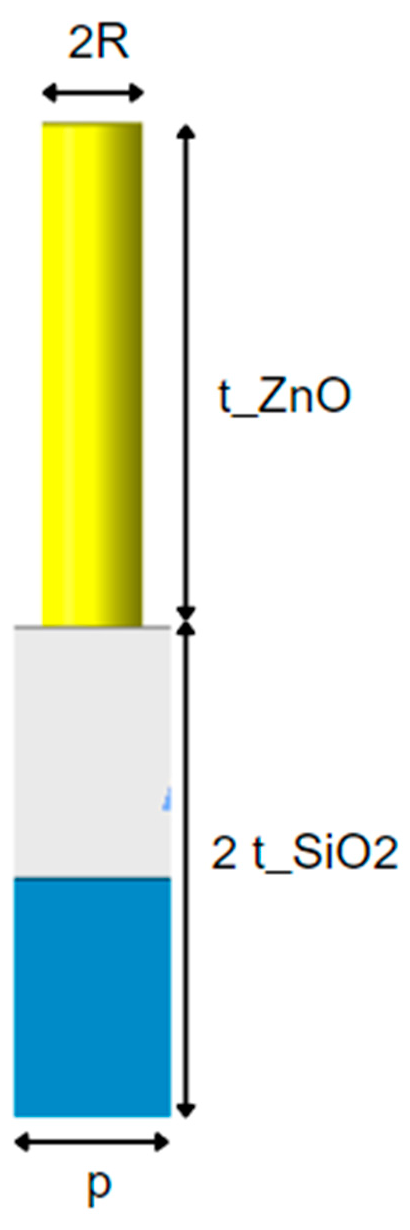
This gives tremendous hope for applications of metamaterials in any telecommunication frequency range, opening up a new domain of its usability to photovoltaic efficiency enhancement. The focus of this study, being a zinc-oxide nanorod mounted to a dual-layer SiO
2-Aluminium-ground is modelled off of the artificial periodic structure fabricated by low temperature hydrothermal methods by
Abhishek Kumar et. al. [
4] previously indicating a performance enhancement for high-frequency bands up to a 50% increase in absorption in the near-UV spectrum. Aside from this, ZnO nanorods have become popular periodic structures for instrumentation techniques for the evaluation of physical/chemical processes [
11]. Hence, this study carries the properties of ZnO into a unique intersection between RF and silicon photonics with emphasis on the Terahertz region, to gauge the rod’s multifunctional properties at the nanoscale.
3. Results and Discussion
Angularly resolved return loss and normalized impedance values were generated with a three-dimensional geometry of the unit cell, such that the nanorods were parallel (Transverse Magnetic (TM) mode) to the polarized incident light [0
2.2. Unit Cell Preconditions and Protocol] during interaction with a varying alternating current (AC) signal. The simulation was performed with a parameter sweep, where frequency interpolation happened at a preset limit of 1 convergent pass. The solution data is far from plasmonic behavior and can be judged accurately.
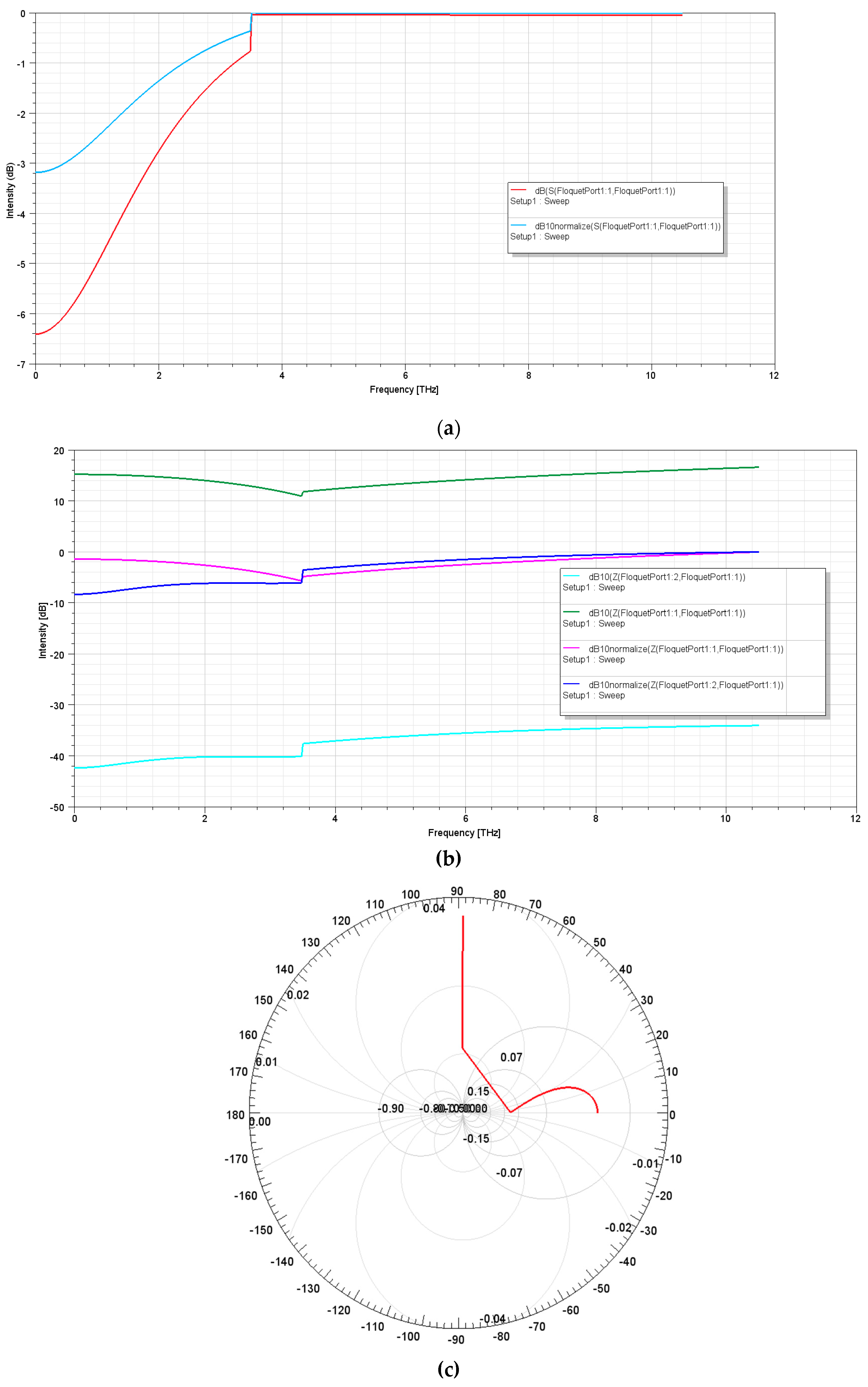
Figure 2.
(a) has been calibrated to display how much of incident energy has
not been reflected back to the source [Reflection Coefficient, Ґ].
Figure 2.
(a) demonstrates a significant phase shift at approximately 3.55THz for both dB and dB10 normalized scales, minimizing the Return Loss of the unit cell to less than -0.1dB up until near-infrared wavelengths of incident light, implying almost perfect matching of the surface in the middle-to-high THz frequency broadband.
We can see that by Impedance Matching Theory, the same balance between the source and the load is maintained in Z-parameter results;
Figure 2.
(b) indicates a similar shift in the magnitude-phase factor at 3.55THz. An exact magnitude-phase diagram has not been produced since the interest is in the reflectivity and transmittivity coefficients, but an S-parameter plot between THz frequency and the phase angle of the input and transfer wave-ports can be generated to further analyze the specific locations of the destructive interference. This would help understand the components of complex impedance shown in
Figure 2.
(c) although not entirely necessary to make informed conclusions about matching in Ґ. At 3.55THz in
Figure 2.
(b), the Ohmic scaling difference between the input and transfer impedances corresponding to |Z11| and |Z21| (i.e., Z-{Floquetport 1:1} and Z-{Floquetport 1:2}), is shown to be approximately -14.23Ω, corresponding to a magnitude difference of approximately 26.5dB. This shows relatively good impedance matching, and extremely good impedance matching for a normalization of 10Ω, therefore aligning with the principal antireflection observed in
Figure 2.
(a). The significant difference between |Z11| and |Z21| also shows that for the characteristic impedance demonstrated by the convergence between the pink and blue traces (evidently and correctly normalized at 0dB), significant power transmission from the source to the load is occurring, therefore resulting in high signal integrity and minimized reflection at the source S-{Floquetport 1:1}. Power transfer ideally tends to a maximum (difference < 20Ω). While the achievement of antireflection for a unit cylindrical ZnO surface is a tremendous step further in the evaluations of the reflective and transmissive properties of similar meta-surfaces dealing with THz propagation, significant power dissipation in the near-MW region is observed as shown by the complex (capacitive) impedance value (red trace on the imaginary axis, 90
° on Smith Chart) as shown in
Figure 2.
(c). The location of the central complex maximum corresponds to roughly 40
°, indicating an imaginary value of 6.59 Ω in polar form [
]. This is the magnitude of the reactance component that corresponds to the upper threshold for perfect impedance matching, the far left of which is purely imaginary (frequency band of approximately 1.4GHz-500GHz), indicating an extremely high loss tangent at significantly longer incident wavelengths. This can in part be due to the conductive properties exhibited by the nanorod in a low-frequency carrier mode, if not for only dielectric loss, but power transmission is still highly inefficient.
The inferences made about power dissipation suggesting the loss of the cylindrical structure occur
after absorption through the excitation of the waveguide, and are further supplemented by
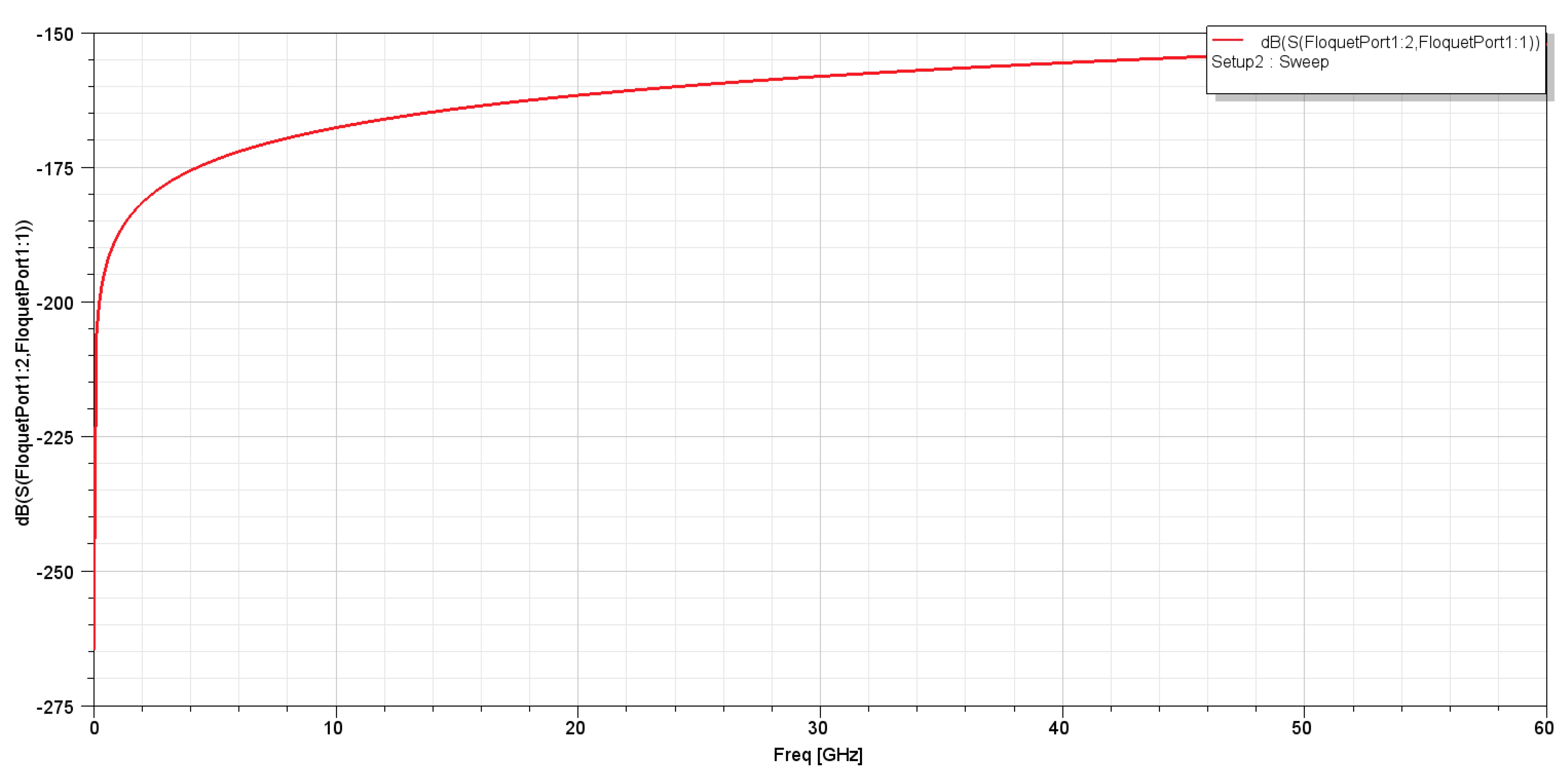
Figure 3., which shows an infinitesimal broadband transmission between ports. Across the broader Terahertz region, till 60THz, a second sweep was setup with 50 passes a sweep interpolation count of 501. The effective transmission coefficient of the film is now estimated to be extremely marginal. A transformation to slighter linearity is observed at the phase shift. While this shows all results are coherent, the Insertion Loss value of -175 dB (corresponding to an |S21| transmission coefficient value of 1.63e-9 [Transmission Coefficient, S21]) reflects a highly negative imaginary component of permittivity contributing to the surface’s dissipation factor. The metamaterial’s negative dielectric constant has been successfully achieved simultaneously with high dielectric loss and low real permittivity ε’.
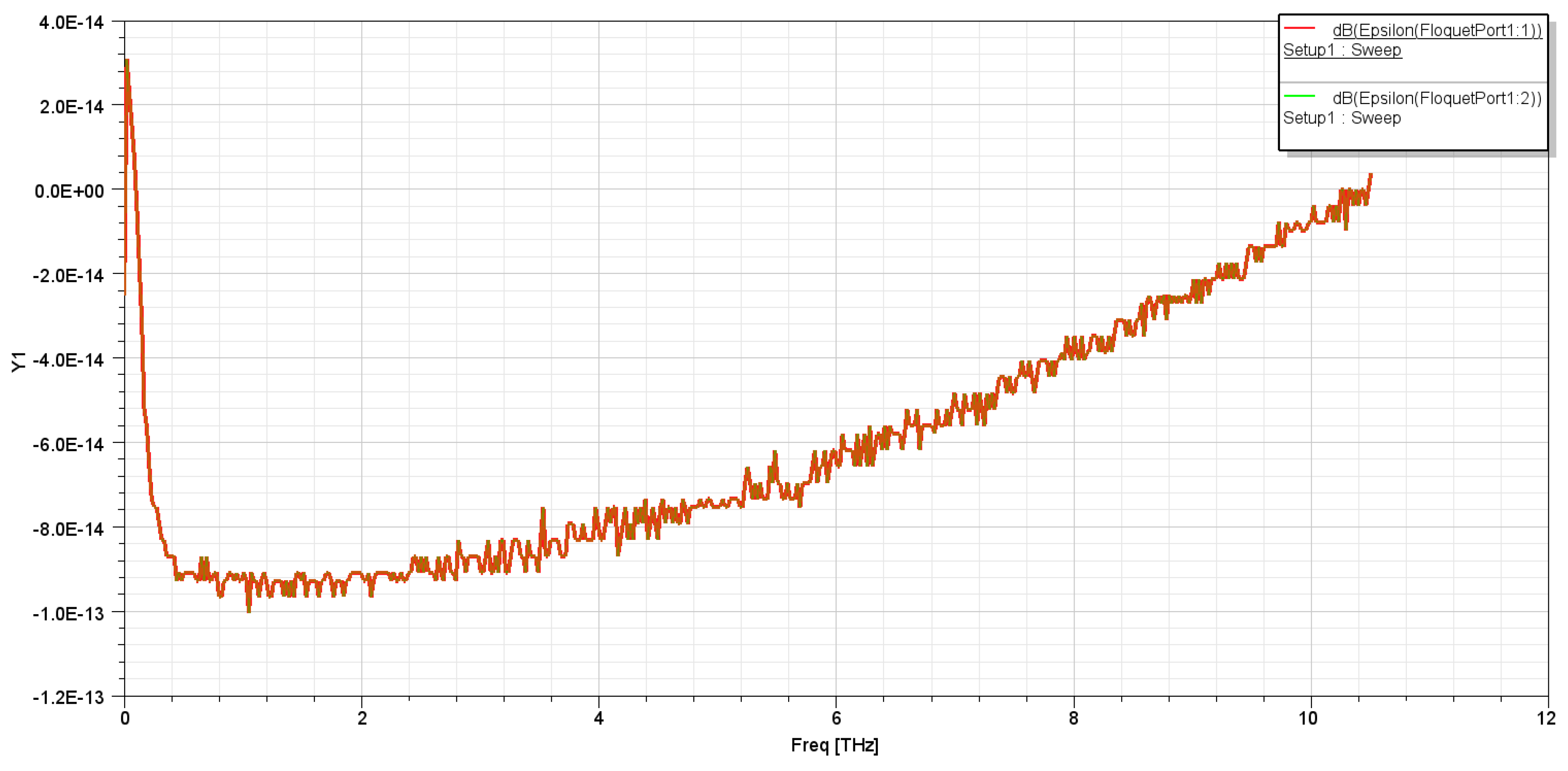
Figure 4. shows almost no transmission to the load, with magnitude of -272 F/m at 3.55THz. The Epsilon Chart also demonstrates there is no location, both in terms of frequency and location on the transmission line from Port 1 to 2, where the nanorod is purely non-dissipative, suggesting that the majority of dissipation observed could be due to heat. The axis values in
Figure 4. along with the correlation of |ε| to speed suggest the refractive index of the unit cell is very high in magnitude.
Connecting this back to
Figure 2.
(a), calculating Ґ for a range of frequencies [Reflection Coefficient, Ґ] demonstrates over 50% of reflectance at 400-600GHz, well within the far Terahertz frequency but still distant to the adjusted magnitude of the phase shift in antireflection. Such drastic changes in spite of good real n-impedance of the input port in the MW band might be due to internal reflections rather than a single interface reflection. This could also explain the observation of high reactance, and subsequently, high inefficiency in
Figure 2.
(c), where impedance matching is achieved at the source, but overall reflectance appears only to be minimized when the impedance matching network is adjusted specifically at 3.55THz. Internal reflectance would imply a unique case with ZnO acting as a conductor, since very high conductance observed in
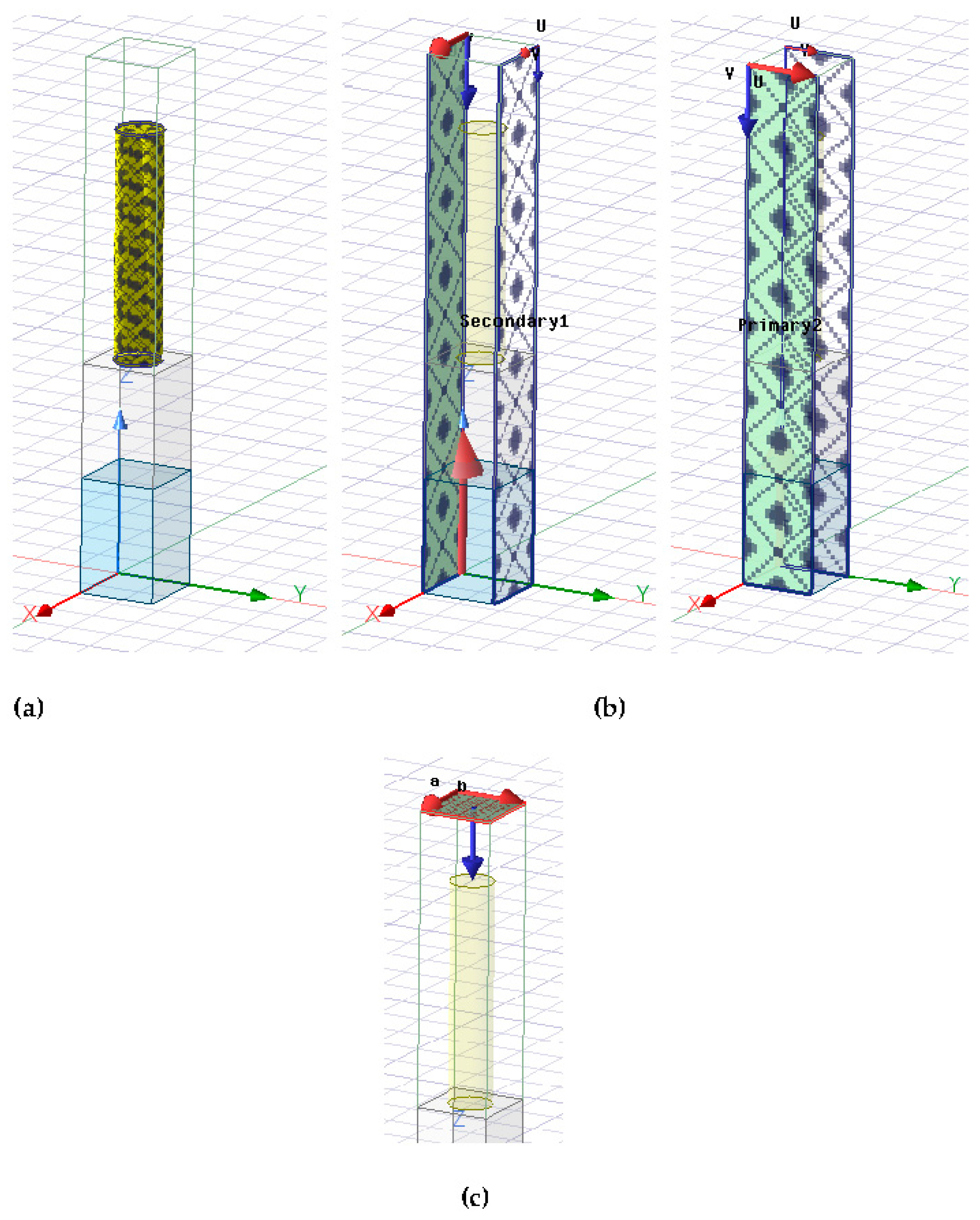
Figure 2. in its entirety is surely a contributory factor, but is most likely due to the geometry of the rod when treating the unit cell as a metamaterial film. That is, high dissipation could stem from the assignment of the “PerfE1” excitation boundary to the ZnO medium (
Appendix A) for graded irradiation through the structure’s primary waveguide being a curved surface, but heat loss from the meta-surface instead of storage in the transmission line, thereby explaining the nonlinearity of
Figure 3. when tending towards high-frequency limits. Assuming that P-type/N-type heterojunctions had constituted the multilayer as shown in [
4], i.e., the external influences of a photovoltaic circumstances were applied to the network, the capacitance shown for the low-THz region in
Figure 2.
(c) would be partially transmitted through the RF circuit’s capacitive element (which would agree with past literature deliberating ZnO’s electrical properties in RF applications [
12,
13,
15]), which would change the left regions of all figures substantially, but that would revert to conventional semiconduction. It is highly recommended that this computerized simulation is also replicated in a physical setting using aforementioned methods with artificial ZnO nanorods attached to SiO
2 fibres on a photovoltaic cell so see whether the results of
Figure 2,
Figure 3 and
Figure 4 are purely immutable for the THz broadband as well as broader MW and RF applications of the antireflection philosophy.
3.1. Calculation of Relevant Coefficients
- 2.
Transmission Coefficient, S21
- 3.
Electrical Permittivity and Dielectric Loss Tangent, ε’ and
is calculated using a phase-angle/THz plot (
Appendix B).
Table 3.
Sample approximate derivations (equal intervals) of relevant parameter calculations through [Reflection Coefficient, Ґ][Transmission Coefficient, S21][
] for tracing of functions representing return loss, insertion loss source and load impedance, and real/complex permittivity in
Figure 2,
Figure 3 and
Figure 4, with mathematical method taken from in-built simulation system tools in Ansys HFSS
1.
| Frequency/THz |
|
|
|
|
| 0.5 |
0.527 |
3.162e-10 |
14.543 |
0.056 |
| 1.0 |
0.438 |
5.623e-10 |
24.010 |
0.092 |
| 1.5 |
0.332 |
7.498e-10 |
25.180 |
0.096 |
| 2.0 |
0.259 |
9.441e-10 |
19.992 |
0.077 |
| 2.5 |
0.206 |
1.011e-9 |
14.115 |
0.054 |
| 3.0 |
0.149 |
1.334e-9 |
6.378 |
0.024 |
| 3.5 |
0.087 |
1.585e-9 |
9.116 |
0.035 |
| 3.55 |
0.014 |
1.631e-9 |
21.397 |
0.082 |
| 4.0 |
~0 |
1.778e-9 |
23.735 |
0.091 |
| 4.5 |
~0 |
1.799e-9 |
26.482 |
0.101 |
4. Conclusions
In conclusion, a computerized simulation analysis was performed using Ansys HFSS on the antireflective and transmissive properties of a cylindrical ZnO-SiO
2/ITO-Al metamaterial multilayered unit cell with Terahertz broadband specifications, as a prospective extension of the work done with ZnO nanorods for organic solar photovoltaic UV applications [
4,
6]. The measured S and Z parameters along with insights into dielectric loss and energy storage through an Epsilon chart modelling the dB20-logarithmic real permittivity suggest strong power transmission and extremely accurate impedance matching of the transmission line, but a high power dissipation factor contributing to an |S11| to |S21| dielectric loss. The normalized characteristic impedance in accordance with the sample calculations of
and
support the deductions made about a phase shift at 3.55THz, within the defined region of incoming Terahertz radiation, as well as the minimization of return loss shown by Input S-parameter calculations. The capacitance of ZnO was also applied to impedance matching calculations in brief, and evaluated in detail based on signals of high reactance in the MW band, shown by non-resistivity between the specified GHz range. A speculation was made about the origin of internal power discharge being attributed to the artificial geometry of the metamaterial causing internal reflections independent of the transmission of power through the input wave-port, and its preconditions for photoexcitation. A high negative refractive index was demonstrated throughout the frequency band, with supporting sample values for
.
Low negative dB in |Z11| suggested low impedance, prospectively useful in matching specific pump load conditions when layered onto a semiconductive substrate, although composed of high reactance attributing to the high conductance of the film. Simultaneously, an evaluation of |S21| showed highly negative dB values for insertion loss indicating poor transmission efficiency. data suggests phase angle being a significant contributor to parameter fluctuations, once again possibly due to the surface orientation given that it is not organic and therefore its oscillations are uniform about a non-uniform excitation boundary. The nanorod’s cylindrical structure seems to prove better results for return loss and can be considered for future low-frequency and high-power applications. Although unlikely, degradation beyond the plasmonic mode can warrant some form of high-temperature annealing to test for geometrical defects. However, some specific modifications are necessary for exploration since heat transmission has been demonstrated to significantly disaffect the efficiency of the film, which in the past has been mitigated by 2-dimensional radiation patches perpendicular to polarized light. These risks can be further investigated with the protocols provided.
Since the magnitudes and dielectric loss tangent values are calculated from metamaterial excitation boundaries alone (due to the elimination of P3HT:PCBM and PEDOT:PSS layers), results from this study can be extended in direct Radio-frequency (RF) applications to further understand ZnO’s conductive capacities as its own field, as moderate energy losses require some form of conductive use and the results are fairly acceptable for lower frequency bands such as the experimental broadband of 0.0014-10.5THz. The results overall show that for high-frequency applications like photovoltaics, such a structure is far from optimal and would likely contribute to intolerable energy efficiency or lack thereof, although further simulation in comparison to the past study on organic solar cells is encouraged.
