2.1. Principle of Full-Bridge LC Series Resonant Electromagnetic Induction Heating
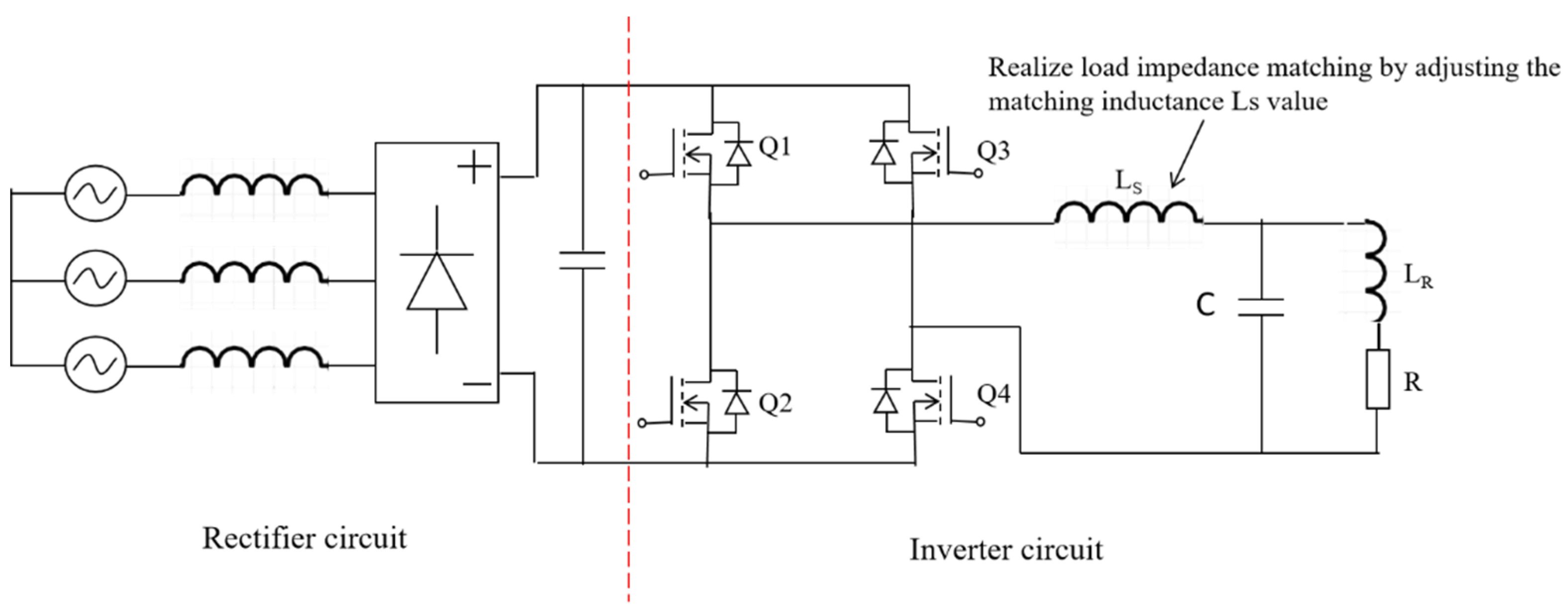
Figure 1 shows the electromagnetic induction heating control system commonly used in industry, which consists of a rectifier circuit and an inverter circuit. The rectifier circuit converts the industrial frequency alternating current (AC) into direct current (DC), and the inverter circuit adopts the circuit structure of full-bridge LLC series resonance, which realizes the inversion of voltage by controlling the two diagonal groups of NMOS to turn on and off alternately. The inversion process refers to the process of transforming a DC voltage into a certain frequency AC voltage. However, the high current with a high-frequency passed through LS usually needs a large size and not suitable for application in small induction heating devices powered by portable lithium batteries. In order to simplify the circuit, a simple full-bridge LC series resonant circuit structure is used in this paper, and the value of R in
Figure 1 can be adjusted via the inverter frequency, thus achieving the load impedance matching.
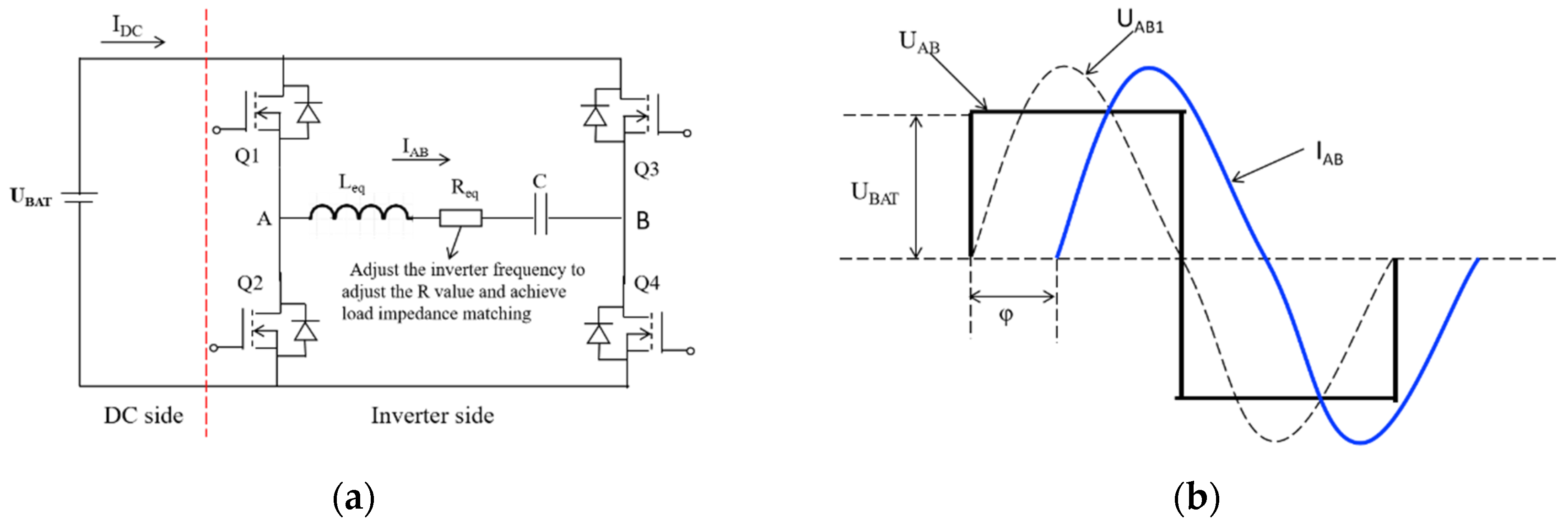
Figure 2(a) shows the structure of the miniaturized induction heating control system. Its structure is mainly divided into two parts: the DC side and the inverter side, where the DC side is the battery side, and the inverter side referring to the inverter circuit side with AC voltage output. U
BAT represents the 3.7V lithium battery supply voltage, and Q1 to Q4 are NMOSs controlled by four independent square wave pulse signals from MCU. L
eq denotes the equivalent inductance of the inverter circuit, R
eq represents the equivalent resistance of the inverter circuit, C is the resonant capacitor of the circuit. By controlling two diagonal groups of NMOS, named Q1,Q4 and Q2,Q3, respectively, alternately turn on and off the lithium battery output DC into AC. The inverter frequency can be adjusted via the frequency control of the NMOSs to achieve the load impedance matching.
Figure 2(b) shows a schematic diagram of the waveforms associated with the circuit. U
AB is the inverter voltage between points A and B. U
AB1 is the fundamental component of the inverter voltage, with a frequency equal to the inverter frequency, and determines the inverter current. I
DC is the direct current from the battery and serves as a monitor for the circuit’s status. I
AB is the sinusoidal current on the inverter side, and φ represents the phase difference, or power factor angle, between the inverter voltage and current.
In a full-bridge LC series resonant control system, the effective value of the fundamental component of the output voltage on the inverter side can be calculated:
where U
DC is the output voltage of the battery U
BAT.
The impedance of the inverter circuit is:
where
is the inverter angular frequency, φ is the power factor angle of the resonant circuit.
Effective value of the inverter side output current:
Inverter side output power:
When the inverter side frequency f equals the resonant frequency of the LC series circuit
At this frequency, the power factor angle of the resonant circuit is 0, meaning that the inductive reactance and capacitive reactance cancel each other out, resulting in a minimum total impedance equal to the equivalent resistance R
eq. The current in the resonant circuit reaches its maximum value I
AB0.
At this point, the voltage across the inductor coil and the resonant capacitor is
where Q is the quality factor of the resonant circuit, given by:
According to Equation (8), at the resonant frequency f0, the voltages across the inductor and capacitor terminals are equal in magnitude but opposite in direction, thus canceling each other out. This ensures that the voltage across UAB1 is effectively applied across the equivalent resistance Req. At this frequency, the voltage across the inductor and capacitor terminals is Q times the root mean square value of the fundamental inverter side voltage UAB1. The quality factor Q is an important parameter of the LC resonant circuit. A higher Q value indicates greater sensitivity of the circuit to frequency variations. In the design of heating systems, as the system transitions from the heating stage to the temperature holding stage, the frequency gradually increases. During this transition, a high Q value effectively suppresses the increase in frequency, thereby reducing the NMOS losses of the transistor.
2.2. Low-Voltage Powered Small-size Electromagnetic Induction Heating Control System Structure and Circuit Principles
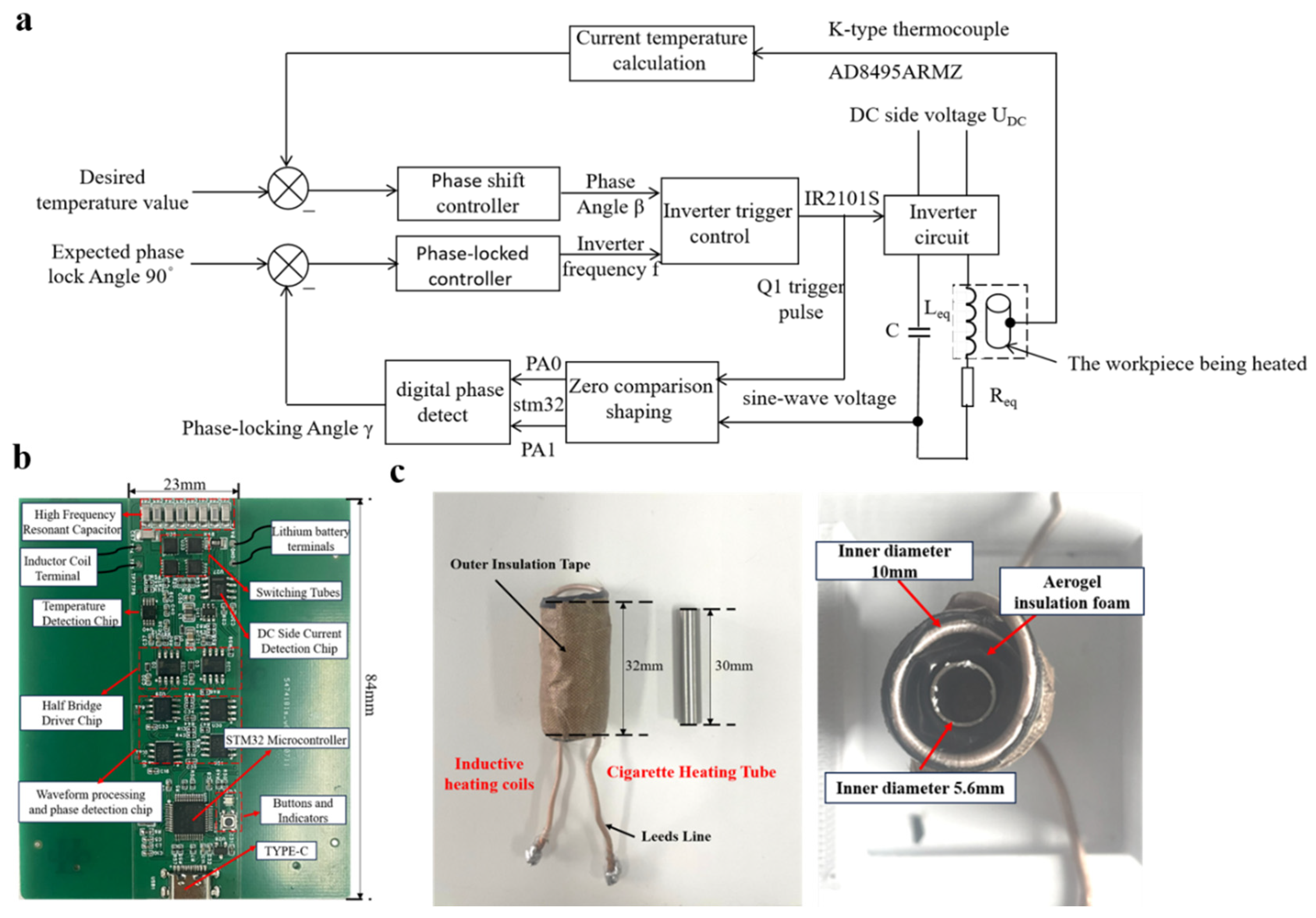
Figure 3(a) shows the overall structural framework of the small induction heating control system, and
Figure 3(b) shows the layout of the PCB circuit board for the specific application of this structure in the design of heating non-combustible smokers. The PCB circuit board has a length of 84 mm and a width of 23 mm, and it is mainly divided into two modules, temperature control and frequency modulation (FM) phase-locked control. The temperature control process requires power regulation, and power regulation requires FM phase-locked control. Therefore, during the system operation, the two modules coordinate with each other to control the duty cycle and frequency of the NMOS drive signal respectively. The NMOSs are controlled through the half-bridge driver chip IR2101S, where the MCU signal input into.
In the temperature control module, a K-type thermocouple and the AD8495ARMZ chip are used to collect temperature data from the heating tube. The difference between the collected current temperature and the target temperature is then inputted into a phase shift controller to update the phase shift angle β, for the purpose of regulating the heating power for temperature adjustment.
In the FM phase-locked loop module, to achieve zero-current conduction of NMOS, it is necessary to ensure that the rising edges of the drive pulses for Q1 and Q4 are aligned with the zero-crossing of the inverter current. Initially, square wave pulse voltages for Q1 drive and sinusoidal wave voltages from resonant capacitors are sampled and shaped through zero-crossing comparison. They are eventually converted into two square wave pulse signals with the same frequency but different phases. The MCU analyzes the phase difference between these two signals and adjusts the frequency through a phase-locked loop controller to achieve a phase difference of 90° between the two signals. This procedure eventually ensures zero-current conduction of NMOS.
In the temperature control process, the heating power is adjusted by the phase shift angle β change, which also will cause the variation of the phase difference between the Q1 drive pulse signal and the inner voltage of the resonant capacitor, and at this time, it is necessary to lock the phase difference by FM phase locking. Therefore, in the control system work, the temperature control module and the FM phase locking module can influence each other and must work in a coordination and balance state.
Figure 3(c) demonstrates the relative positions and dimensions of the inductor coil, heating tube, and temperature holding layer. The inductor heating coil has an inner diameter of 10 mm and a length of 32 mm, and the heating tube has an inner diameter of 5.6 mm and a length of 30 mm. The inductor heating coil and the heating tube are filled with an aerogel temperature holding to minimize the thermal conduction from the heating tube to the inductor coil.
Figure 4 illustrates the driving principles of the full-bridge NMOS configuration. The four NMOSs are controlled by two half-bridge driver chips, with Q1 and Q2 forming one pair and Q3 and Q4 forming another pair. The input to the driver chips consists of two complementary pulse-width modulation (PWM) signals with a dead-time interval, generated by MCU PWM function. During system operation, when Q1 and Q4 are conducting while Q2 and Q3 are off, channel Q3 to Q2 are conducting and channel Q1 to Q4 are off. This alternation of conduction between these two diagonal NMOS pairs then can achieve inversion at terminals A and B. And when the two diagonal NMOS drive pulses are the same, the duty cycle of the U
AB voltage is 50%. When the drive pulses for these pairs are phase-shifted, the duty cycle of voltage U
AB decreases, along with its RMS value. The heating power then can be adjusted.
Figure 5 shows the system FM phase-locked schematic diagram. The INA597 and LM311 are used to process the Q1 drive voltage and the voltage signal on the inside of the resonant capacitor. The INA597 is used to derate the signals to bring the voltage down to within the allowable range of the LM311 input voltage, and the LM311 compares the signals over zero and finally transforms the waveform into a 3.3v square wave voltage. Then two transformed pulse signals are input to the MCU for phase difference calculation, and according to which the frequency is then adjusted and locked. Finally, Q1,Q4 driving pulse is located at the zero crossing point of inverter current to realize the soft turn-on of NMOS.
2.3. Electromagnetic Induction Heating Control System Work Process
This system employs a combined phase-shifting and frequency-locking power adjustment method. By adjusting the duty cycle of the driving pulse signals for Q1~Q4 to increase the phase shift angle β, the value of U
AB1 is changed. Simultaneously, the frequency-locking phase controller ensures that the rising edge of the driving pulse signals for Q1 and Q3 aligns with the zero-crossing point of the inverter circuit, thereby achieving soft switching. The STM32 timer can count cyclically between 0 and the auto-reload value (ARR). CCR is the value of the timer output comparison register. When the timer count value (INT) is greater than CCR, the timer outputs a low level, and vice versa outputs a high level. Therefore, the duty cycle of Q1,Q2 and Q3,Q4 can be adjusted by adjusting the value of CCR, and Q1,Q2 and Q3,Q4 are complementary pulses with complementary duty cycles. The variable X is set within its range of 0~1, and the CCR is adjusted by the variable X. Its relationship with the CCR of the two sets of pulse signals is as follows
where CCR1 controls Q1,Q2 to drive the pulse duty cycle.CCR2 controls Q3,Q4 to drive the pulse duty cycle
.
Figure 6 shows the driving pulses for Q1~Q4 during the system’s power adjustment process, as well as some important waveforms. U
AB represents the square wave voltage on the inverter side, with an amplitude equal to the lithium battery’s output voltage. When Q1 and Q4 are turned on while Q2 and Q3 are turned off, U
AB is positive. Conversely, when Q2 and Q3 are turned on while Q1 and Q4 are turned off, is negative. Thus, the inversion of voltage is achieved by controlling the on/off states of the diagonal pairs of NMOSs. The phase shift angle β is the interval angle between the driving pulses for Q1 and Q3. When the phase shift angle is β, the following applies:
When the phase shift is β, by adjusting the frequency, the zero-crossing point of I
AB is kept lagging behind the rising edge of the drive pulses for Q1 and Q3 by a very small phase shift angle α. The purpose of this adjustment is to provide sufficient time for the NMOS commutation and to approximately achieve zero-current switching. Considering that the voltage across the capacitor always lags the current I
AB by 90°in phase, this paper uses the voltage across the capacitor to phase-lock I
AB, with a phase-lock angle of 90°. By frequency modulation and phase-locking, Q1 and Q3 can be maintained in a soft turn-on and high current turn-off state during the power adjustment process, as shown in the right side of
Figure 6.
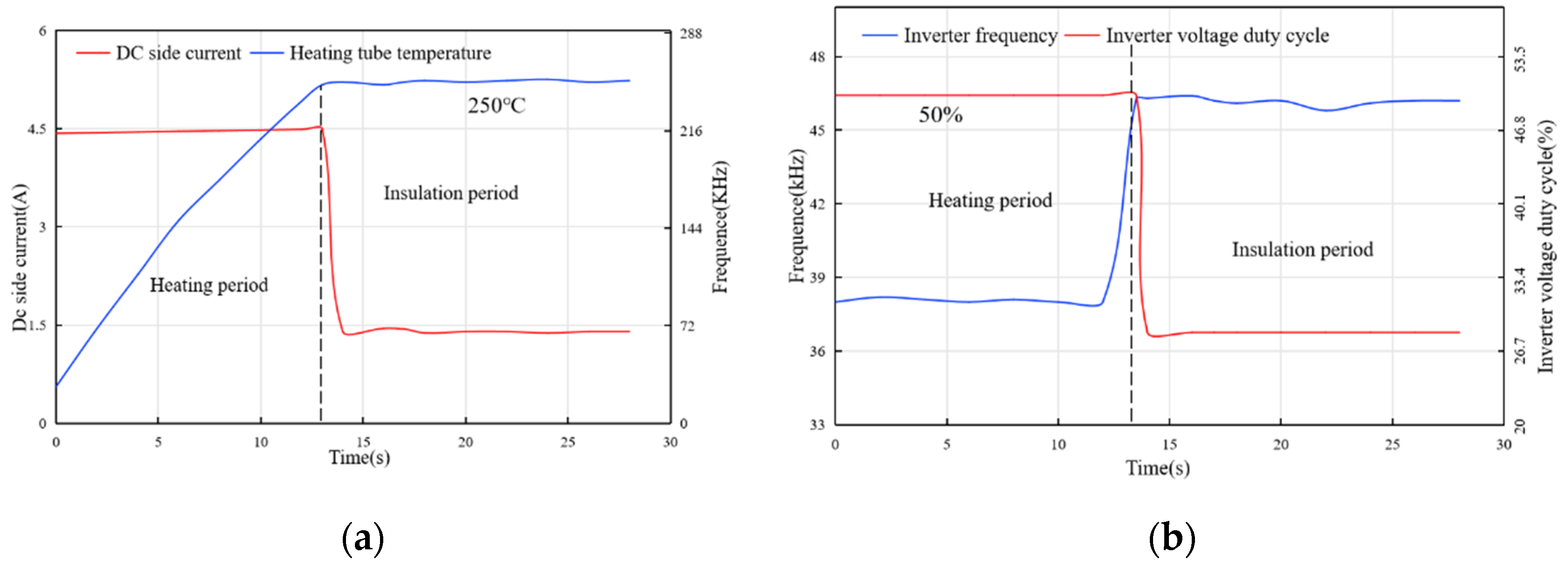
Figure 7 describes the operation process of the heating non-combustion smoking device control system. It shows that the process can be divided into two periods: the heating and the temperature holding period. During the heating period, when the inverter frequency equals the resonant frequency, the duty cycle of the drive pulses for Q1 to Q4 is 50%, at which point X=0, β=0, U
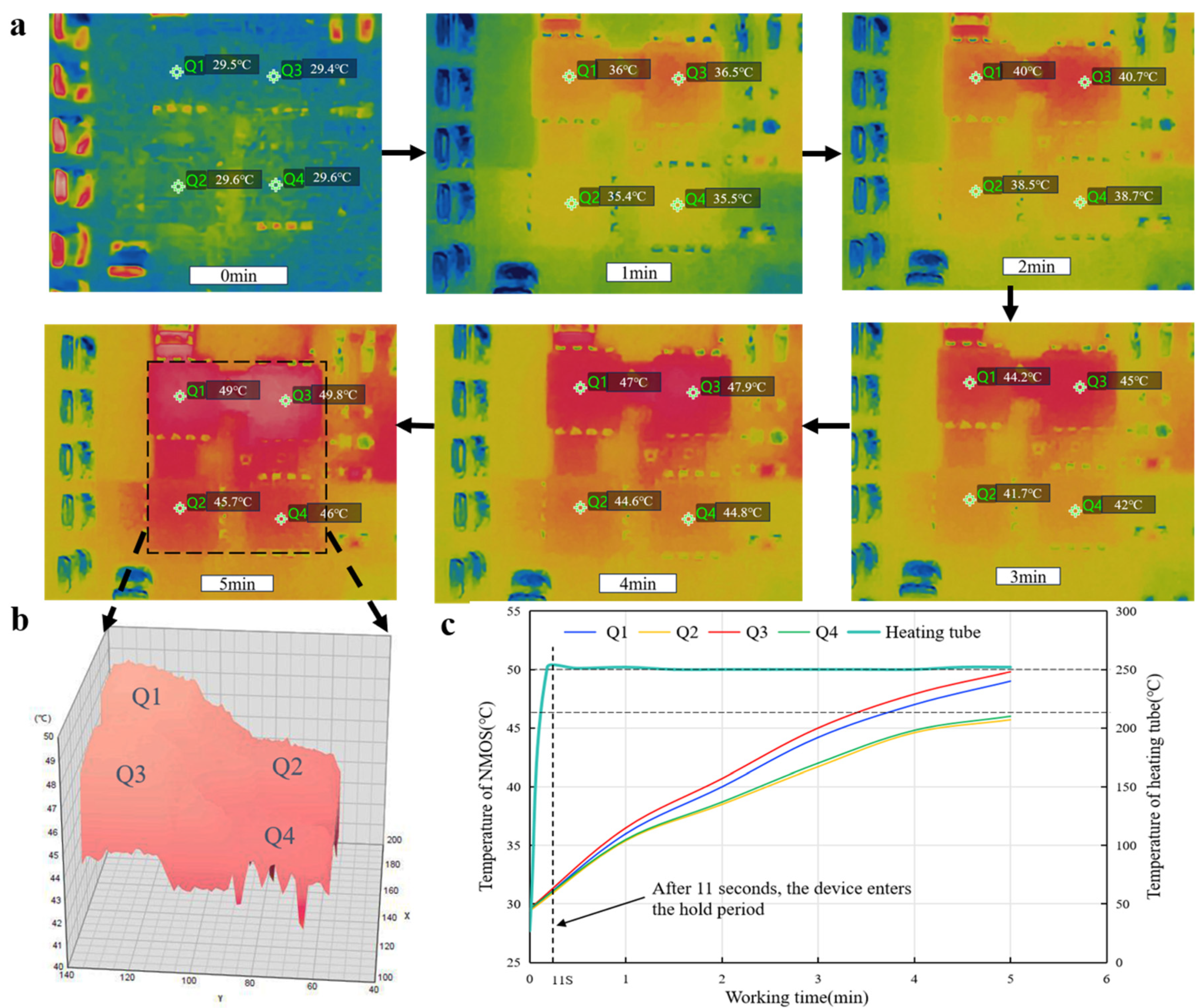
AB1 is at its maximum, and the inverter current is also at its maximum. This state is used to heat the heating element, rapidly raising its temperature to 250°C. At this time, all four NMOSs are in a soft-switching state, effectively avoiding large losses caused by high currents. When the system enters the temperature holding period, the value of X increases, the phase shift angle β increases, and the duty cycles of Q1 and Q3 decrease, while the duty cycles of Q2 and Q4 increase. With the frequency modulation and phase-locked control, the inverter frequency continuously increases from the resonant frequency, causing the duty cycle of the inverter voltage to drop from 50% to about 28%. During this process, the DC side current IDC gradually decreases until it stabilizes, and the temperature of the heating element ultimately stabilizes around 250°C. In the heating period, both the turn-on and turn-off of Q1 to Q4 are in a soft-switching state. In the temperature holding period, Q1 and Q3 are in a soft turn-on and high current turn-off state. The NMOS losses also change in different periods.
2.4. Impact Factors Analysis of NMOS Losses
The total loss of NMOS in the small electromagnetic induction heating control system mainly consists of three parts: the conduction loss and driving loss of all NMOSs in the heating and temperature holding period, and the turn-off loss of NMOS Q1, Q3 in the temperature holding period. In order to optimize the NMOS loss, the above three losses are calculated and influencing factors are analyzed.
In the full-bridge LC series resonant circuit structure of
Figure 2(a), the output power on the DC side is approximately equal to the output power on the inverter side, so the following equation can be obtained:
The inverter current is:
where:
From the waveform relationship in
Figure 8, we obtain:
where β is the phase shift angle and D is the duty cycle of the drive pulses for Q1 and Q3.
Substituting into Equation (13):
At this time, the off-state current in the circuit is:
where θ is the angle corresponding to the high level of the Q1 pulse.
From the circuit state relationship:
Substitute into Equation (20):
From the analysis of the
Figure 8, it can be seen that the switching states of the diagonally opposite switches directly determine the direction and duty cycle of the inverter-side output voltage. Therefore, the diagonally opposite switches are grouped into pairs: Q1 and Q4 form one group, while Q2 and Q3 form another group. Since these two groups are symmetrical, only the loss analysis of Q1 and Q4 is required, where Q1 is the upper bridge arm and Q4 is the lower bridge arm.
The conduction loss calculation formula for Q1 and Q4 is approximately:
Substitute I
AB from Equation (14) to obtain:
where D is the duty cycle of the Q1 driving pulse. During the heating period, D=0.5, at which time:
The calculation formula for the driving loss of Q1 and Q4:
where V
DR is the NMOS’s driving voltage, f is the inverter-side frequency, and Q
g is the total gate charge of the NMOS. During the heating and temperature holding periods, the driving losses of Q1 and Q4 are the same.
From the above analysis, during the heating period, there are no turn-off losses for Q1 and Q4, while during the temperature holding period, only Q1 introduces turn-off losses.
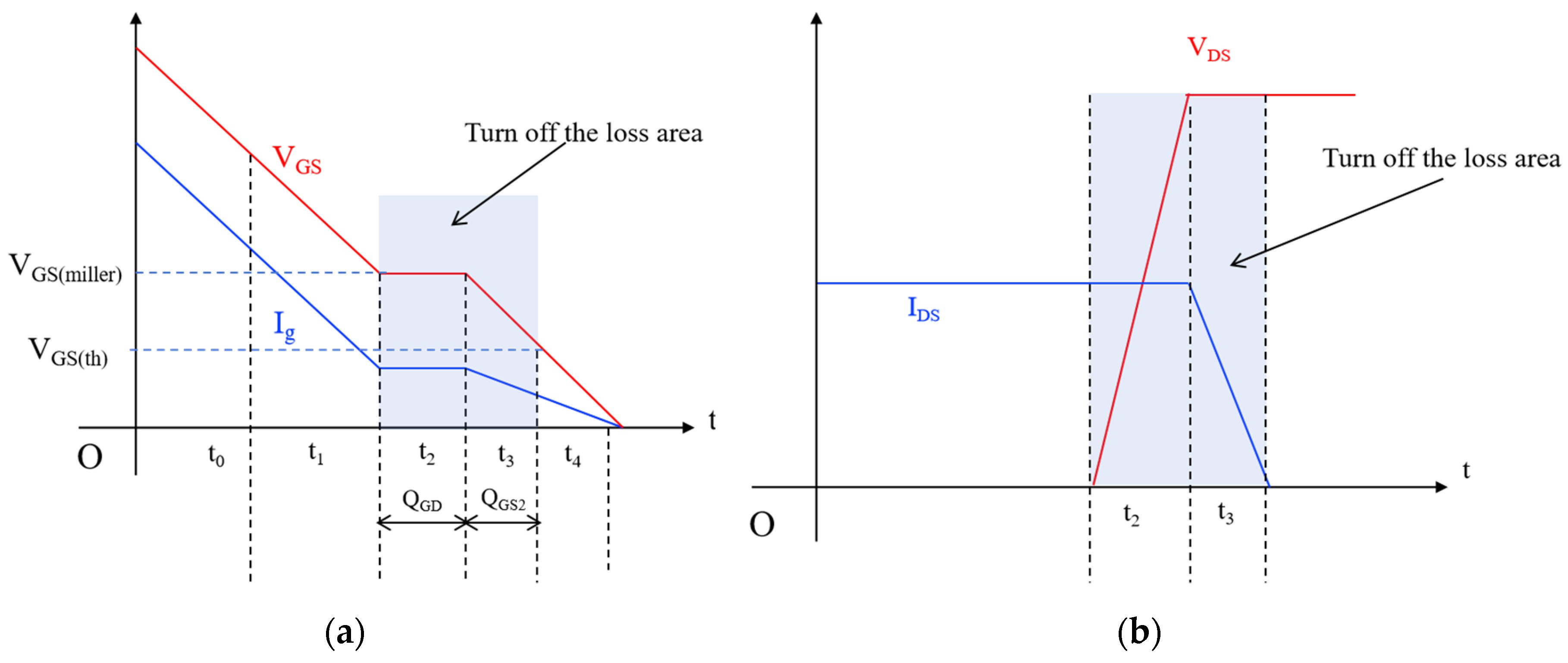
Figure 8 shows the variation of parameters during the turn-off process. V
DS is the NMOS drain-source voltage, I
DS is the NMOS drain-source current, V
GS is the NMOS gate-source voltage, V
BAT is the battery supply voltage, and I
g is the NMOS gate drive current.
It is observed that the turn-off process mainly consists of two stages: t2 and t3. In stage t2, IDS remains constant, and VDS rises rapidly to the VBAT. During this stage, the VDS and gate driving current remain unchanged, and the VDS is at the Miller plateau(A time period in which VGS is held constant and the VDS voltage gradually rises or falls under the action of Ig); the charge discharged in this stage is denoted as QGD. In stage t3, the VDS remains constant while the current drops quickly to zero. During this stage, the VDS drops to VGS(th), and the gate driving current decreases; the charge discharged in this stage is denoted as QGS2.
Based on the geometric relationship in
Figure 8(b), the Q1 turn-off loss during this stage is approximately:
where f is the inverter-side frequency, U
off is the turn-off voltage, which is equal to the lithium battery supply voltage. I
off is the turn-off current, which is calculated using Equation (21). t
off is the turn-off loss time, consisting of two parts: t
2 and t
3. where
The total loss of Q1,Q4 during the heating period is
And at this time Q1,Q2,Q3,Q4 have the same loss of power
During the holding time, the total loss of Q1,Q4 is
At this time, the losses of the upper bridge arm NMOS Q1,Q3 are the same, and the losses of Q2 and Q4 are the same.
Figure 9(a) shows the trend of Q1’s conduction loss with varying inverter-side duty cycle under different DC-side currents I
DC and its own on-resistance R
DS(on). It is clear that the conduction loss decreases with the increase of the inverter voltage duty cycle, regardless of the conditions. Additionally, for a constant R
DS(on), the loss increases with increasing I
DC. For a constant I
DC, the loss increases with increasing R
DS(on), and Q4 exhibits the same variation pattern as Q1.
Figure 9(b) illustrates the trend of the driving loss of the NMOS with increasing inverter frequency f under different gate total charges Q
g. It is found that its loss increases with increase in inverter frequency and increases with increase in its own Q
g.
Figure 9(c) shows the trend of Q1’s turn-off current as the inverter-side duty cycle changes under different DC-side currents I
DC. It shows that for the same IDC, the higher the duty cycle, the lower the shutdown current. At the same duty cycle, a larger I
DC corresponds to a larger turn-off current.
Figure 9(d) demonstrates the trend of Q1’s turn-off loss with varying turn-off current under different turn-off times t
off and inverter frequencies f. It can be seen that the turn-off loss increases as the turn-off current increases in any case. Furthermore, for a constant t
off, the loss increases with increasing f. For a constant f, the turn-off loss increases with increasing t
off.
The above analysis reveals that the conduction loss of the NMOS is mainly related to its own on-resistance RDS(on), the DC-side current IDC, and the inverter-side duty cycle D. The driving loss is primarily influenced by the inverter frequency f, the NMOS’s own parameters Qg, and the driving voltage VDRV. The turn-off loss is mainly associated with the turn-off time toff, the turn-off current Ioff, and the inverter frequency f, where the turn-off current is primarily determined by the DC-side current IDC and the inverter-side duty cycle D.
2.5. Experiment Setup
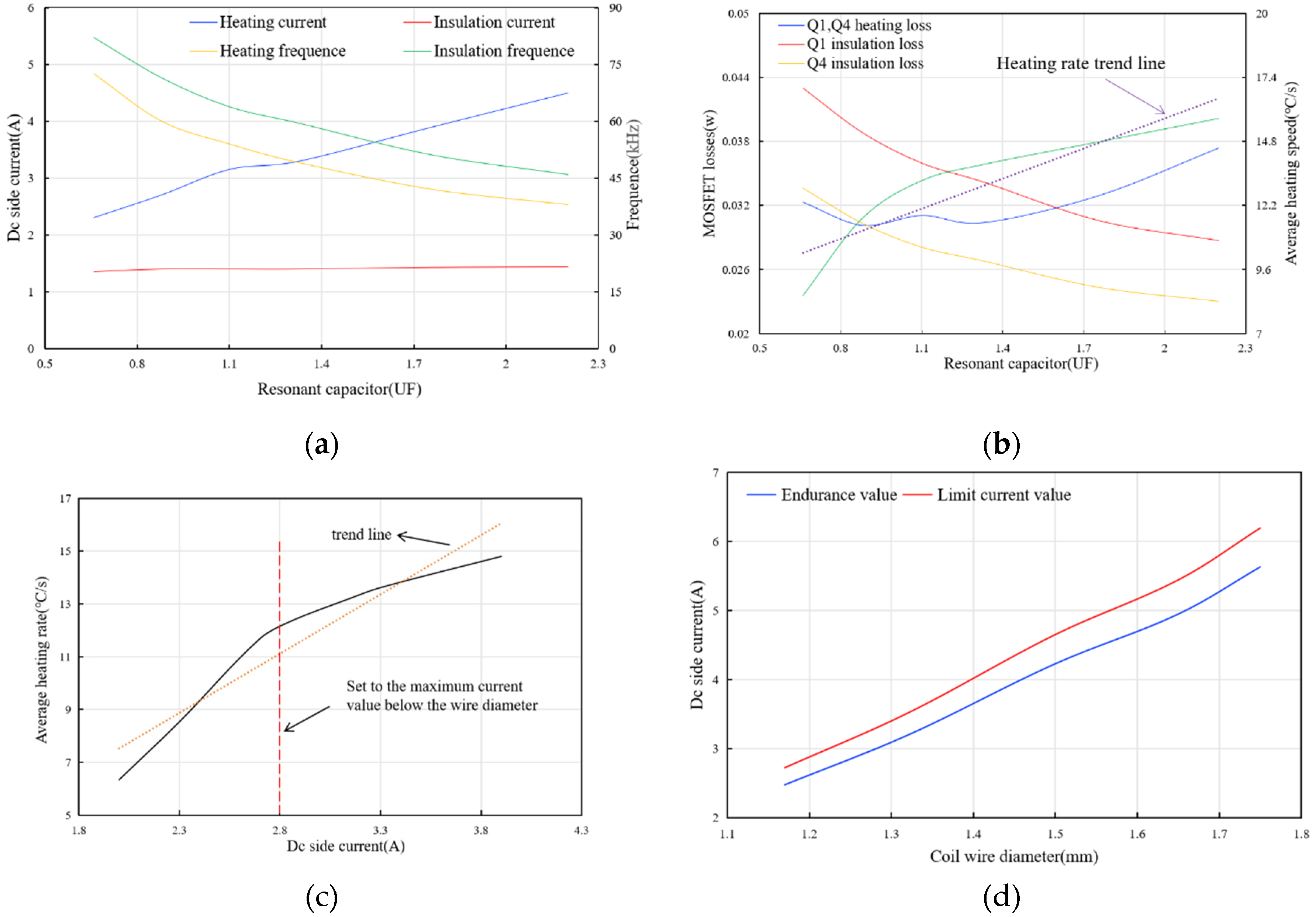
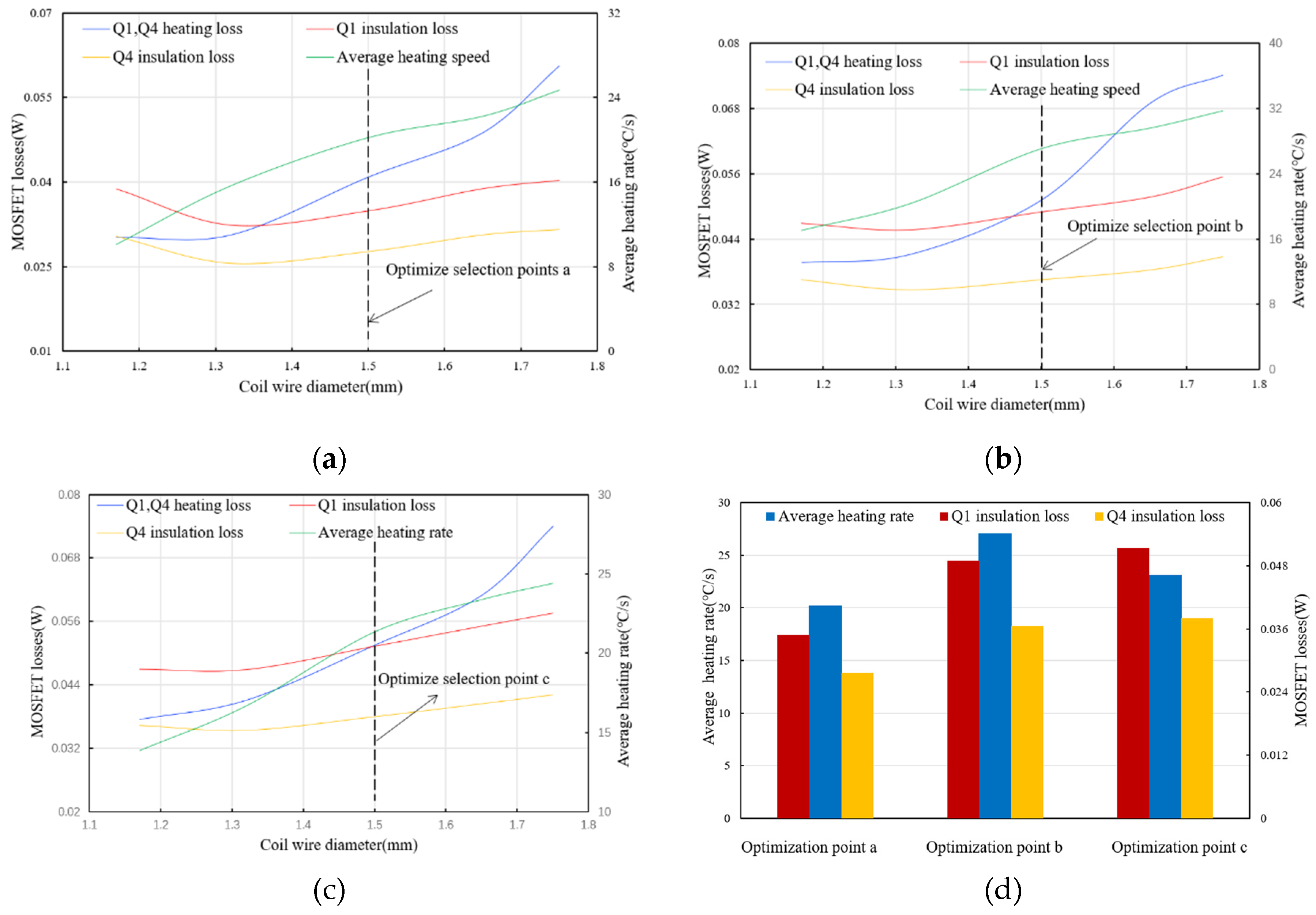
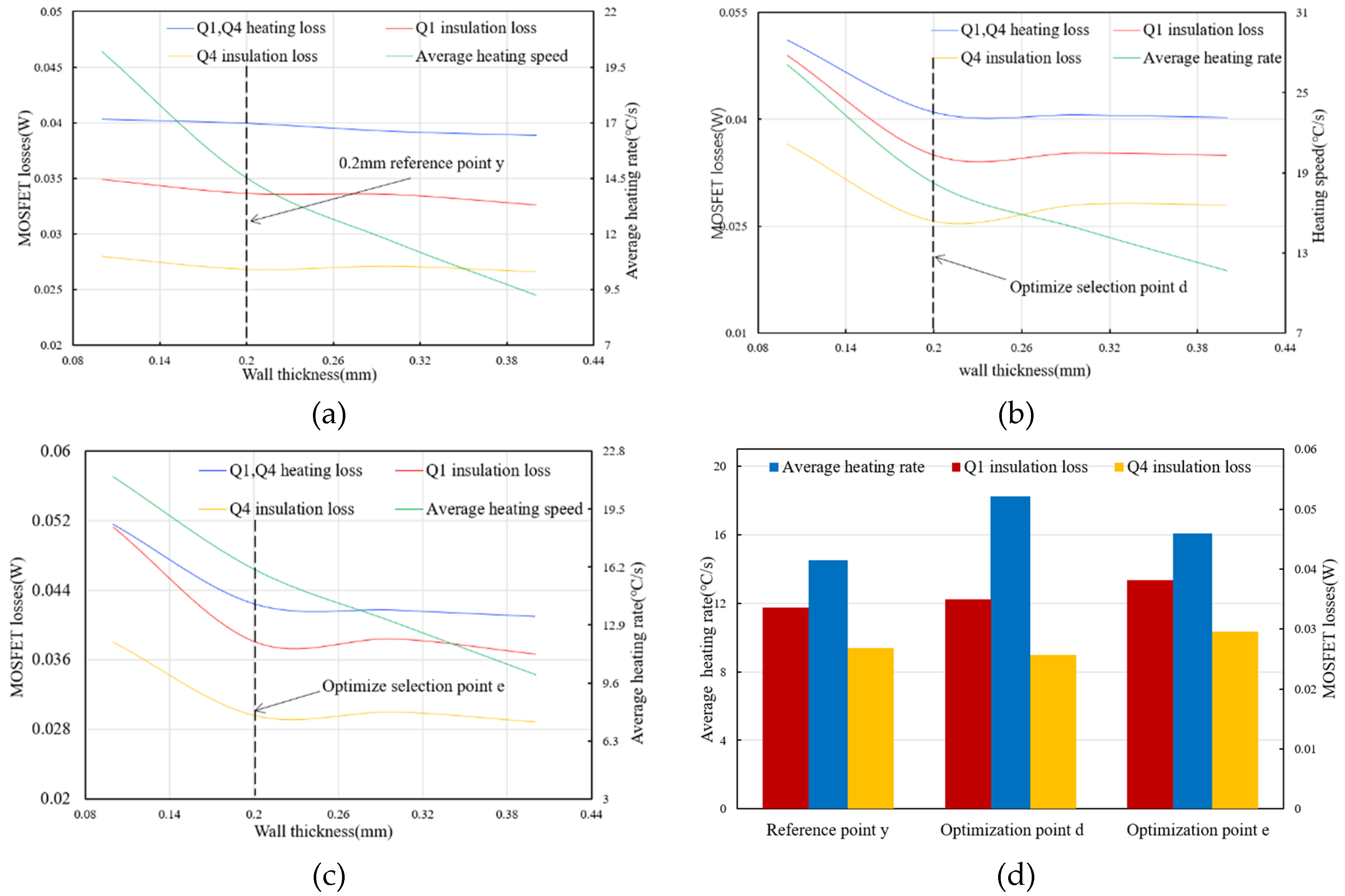
To improve the performance of the control system, the influence of circuit parameters including resonant capacitance value, the wire diameter of the induction heating coil, the material and wall thickness of the heating tube on the performance of the heating system was studied through experiments.
Experiments were conducted using a 1.17mm induction coil wire diameter to explore the impact of capacitance changes on the heating rate of the tube and to calculate the NMOS total loss value at each stage simultaneously for the control system’s performance. To investigate the effect of different induction coil wire diameter, experimental tests are carried out on coils with five wire diameters of 1.17, 1.32, 1.5, 1.65 and 1.75 mm. The heating rate of the heating tube is recorded at different capacitance values, and the NMOS total loss value are calculated at each stage. Three commonly used representative materials in induction heating, Iron, 430 stainless steel, and 1J50 soft magnetic alloy, were selected for experimentation.
Table 1 shows the physical parameters of the three materials. At the same time, in order to investigate the effect of wall thickness on the performance of the control system, heating tubes with different wall thicknesses of 0.1, 0.2, 0.3, and 0.4 mm were employed to investigate the effect of wall thickness on the heating rate and the NMOS total loss.
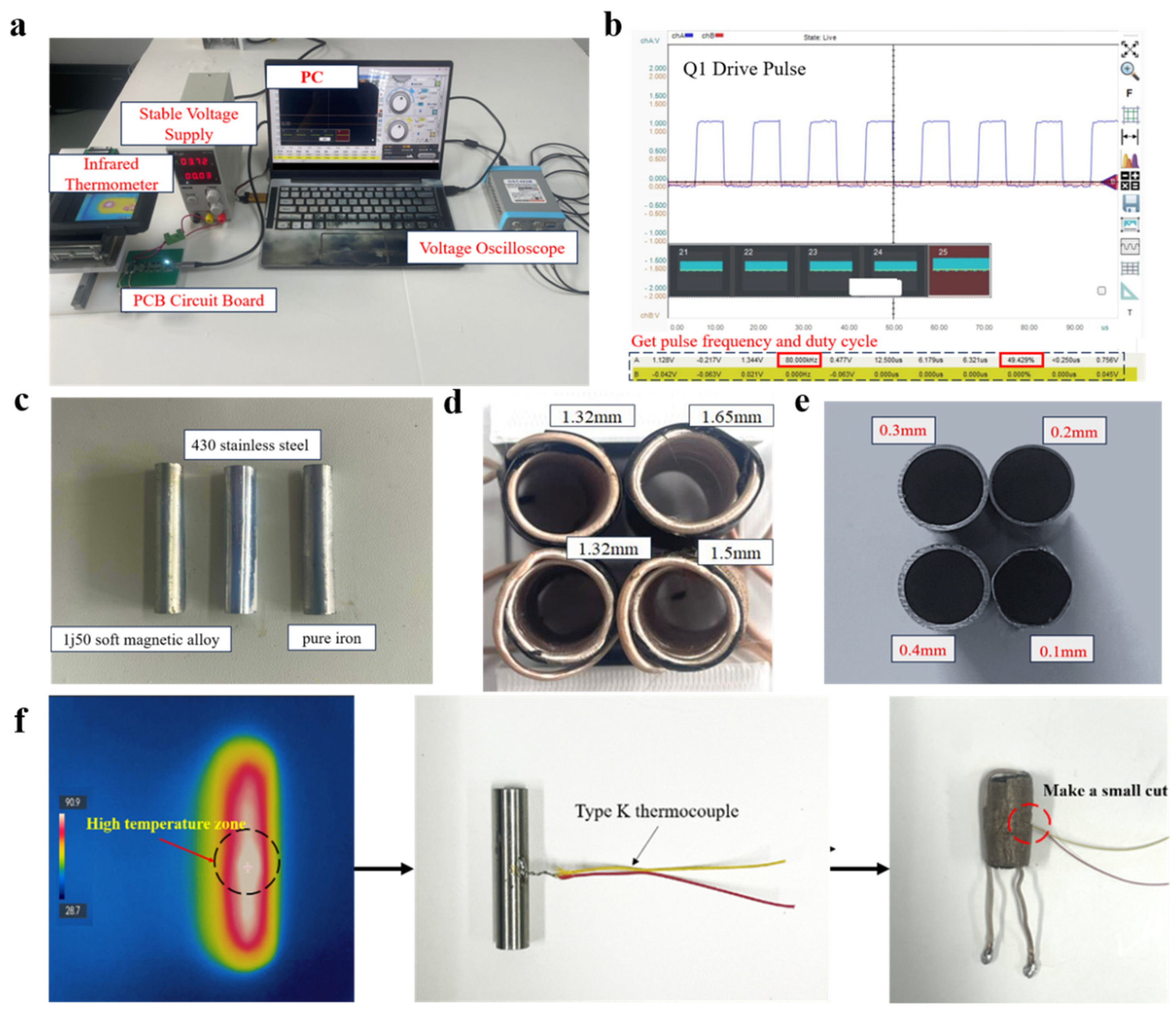
Figure 10(a) displays the experimental setup for evaluating the performance of a small electromagnetic induction heating control system. A regulated power supply replaces a 3.7V lithium battery to enable easier monitoring of output current. Program commands were sent from PC to the control system MCU and monitors the frequency and duty cycle of the oscilloscope’s output waveforms during the experiment. An infrared temperature meter measures the actual temperature rise of the NMOS.
Figure 10(c), (d), and (e) compare the appearance of materials used, the wire diameter of the induction heating coil, and the wall thickness of the heating tube, respectively.
Figure 10(f) illustrates the method used to measure the heating rate of the tube: an infrared temperature measuring instrument observes the temperature distribution, revealing a ladder-like pattern with the highest temperature in the middle. To precisely control this peak temperature, a K-type thermocouple is positioned at the center of the heating tube. A small opening is cut in the middle of the induction heating coil to guide the thermocouple, preventing temperature drift caused by the coil’s high-frequency magnetic
