1. Introduction
Ultrasonic testing technology utilizes the propagation characteristics of ultrasound in materials for non-destructive testing (NDT) of defects, foreign bodies, and cracks [
1,
2,
3,
4]. This method offers high sensitivity, strong non-destructiveness, broad applicability, real-time analysis, quantifiability, and safety, making it highly efficient and valuable in the NDT field. It is also widely employed in industries of iron and steel, petrochemicals, aerospace, and nuclear power [
5,
6,
7,
8,
9].
Ultrasonic transducers are crucial to the ultrasonic testing system, as they transmit and receive ultrasonic waves, comprising either single-element or multi-element designs [
10,
11,
12,
13]. Capacitive micromechanical ultrasonic transducers (CMUT) are emerging as a novel and promising alternative to conventional bulk PZT (lead zirconate titanate) transducers, offering advantages in miniaturization, integration, and performance [
14,
15,
16]. While CMUTs have been primarily explored for medical ultrasound imaging [
17,
18,
19], their application in NDT is less developed.
This study presents the design, fabrication, and characterization of a CMUT transducer for NDT, consisting of two elements. The ultrasonic transducers function as actuators to generate ultrasonic waves and as sensors to detect these waves. This study also includes the development of a custom ultrasonic imaging transceiver system for transmitting pulses and receiving echo signals. We detect defects using sensors and determine the severity of defects to validate the potential of CMUT transducers in NDT applications.
2. Materials and Methods
2.1. Transducer Structure
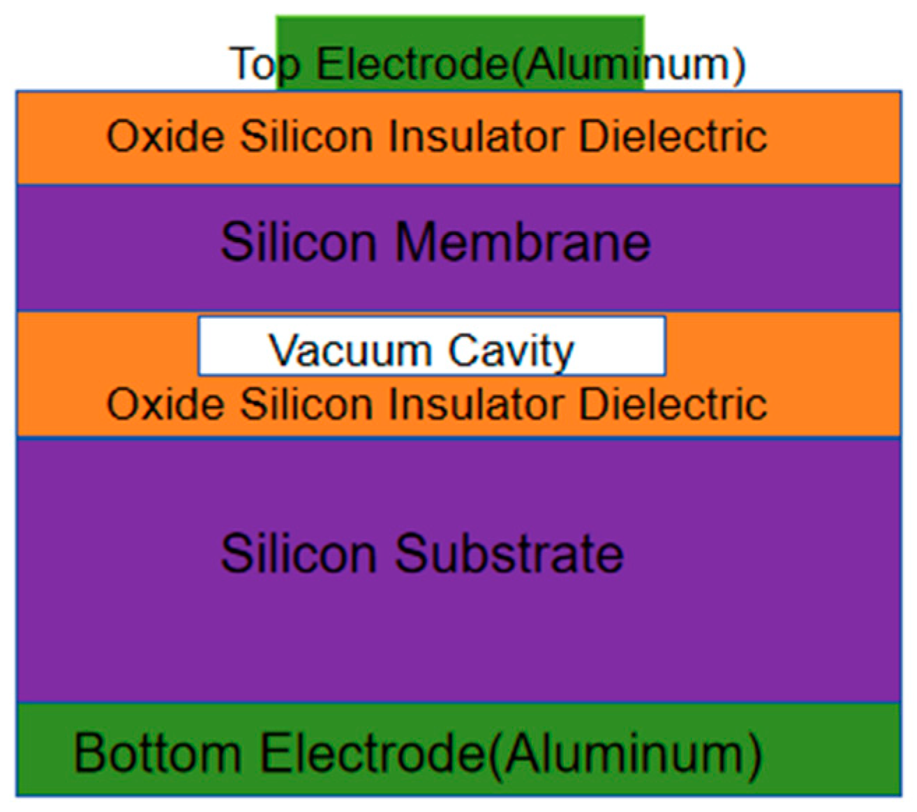
The CMUT transducer comprises multiple sensitive capacitor units, each including a metal top electrode, a vibrating film, an isolating layer, a vacuum chamber, an insulating layer, a silicon substrate, and a metal bottom electrode. The sensitive unit structure of the CMUT transducer designed in this study is illustrated in
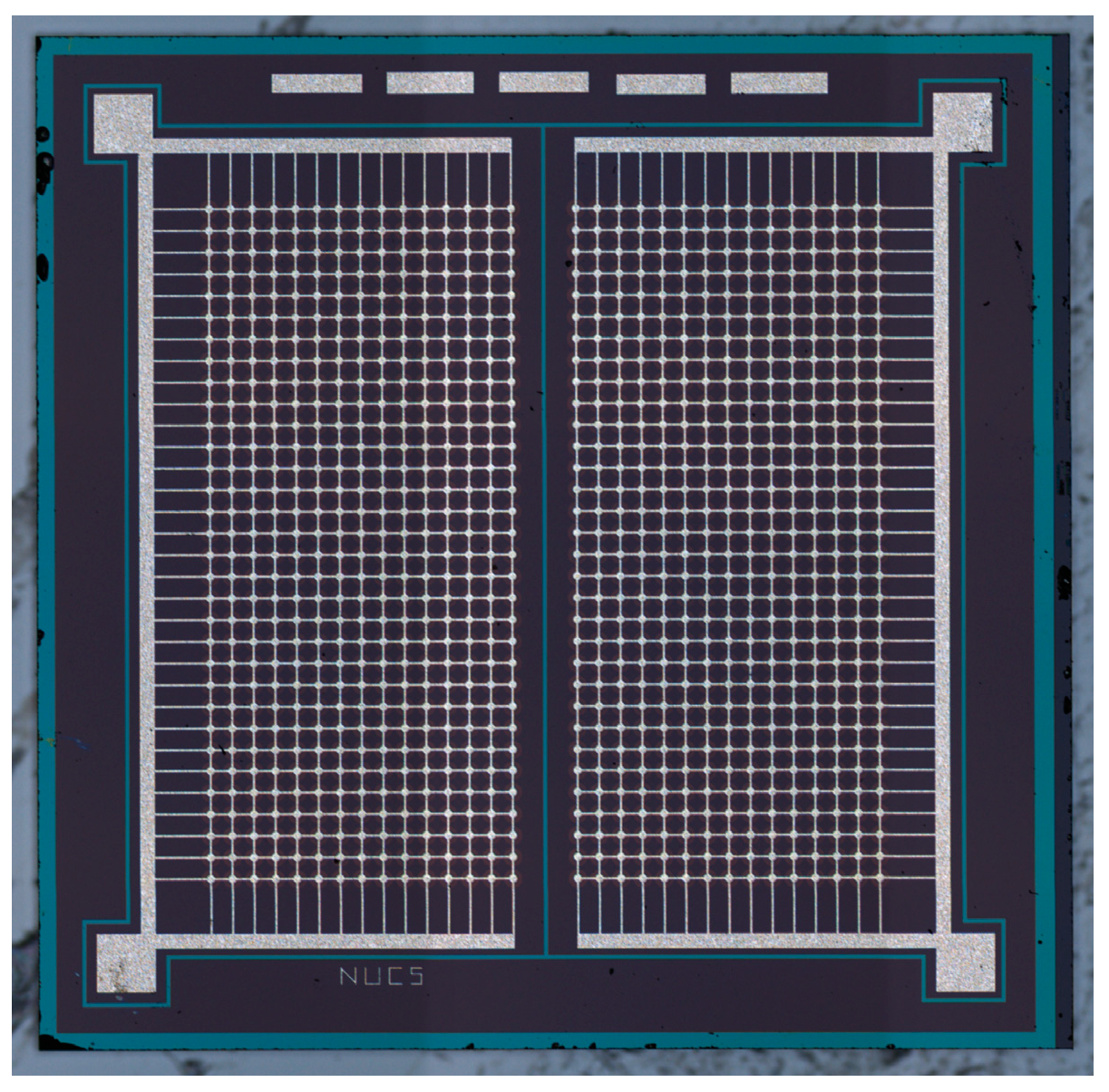
Figure 1. The top and bottom electrodes are created by sputtering aluminum, while the vibrating film consists of the top layer silicon of silicon-on-insulator (SOI), offering excellent uniformity and consistency. The vacuum cavity and the insulating layer provide good insulation to prevent short circuits between the highly doped conductive silicon sheet and the silicon substrate during operation, even in collapse mode. The silicon oxide isolation layer between the top electrode and the vibrating film reduces the parasitic capacitance of the sensor. The silicon substrate supports the insulation layer and the vibrating film, and forms an ohmic contact with the metal electrode, constituting the fixed plate of the CMUT transducer. The CMUT transducer includes 900 capacitor units arranged in parallel and divided into two arrays (
Figure 2). During fabrication, the silicon film is 2-μmthick, and a silica insulation layer with a thickness of 150 nm is retained between the vacuum chamber and silicon substrate. The parameters of the CMUT transducer are detailed in
Table 1.
2.2. Capacitive Micromachined Ultrasound Transducer Fabrication
The CMUT device was fabricated using silicon fusion wafer-bonding technology, which involved directly bonding two silicon surfaces at high temperatures, resulting in high bond strength and extreme hermeticity [
20]. This wafer-bonding approach was chosen because it facilitates easier fabrication of membrane structures from silicon wafers.
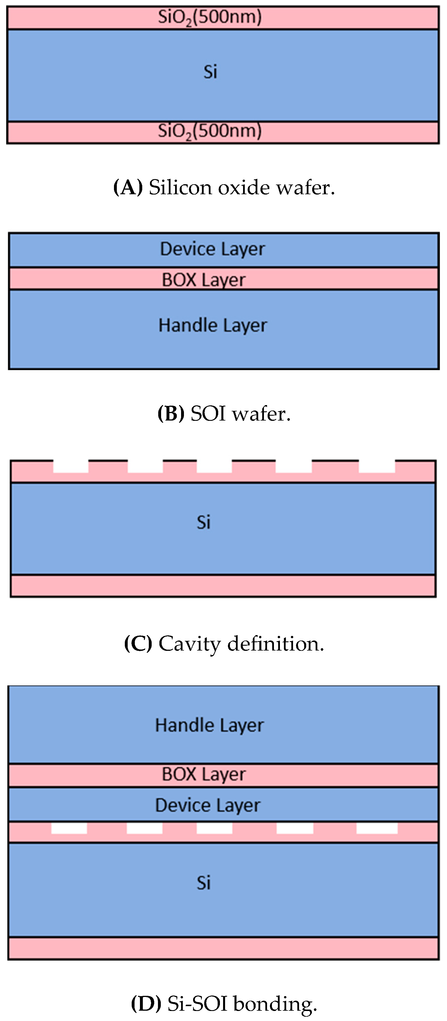
The process began with two wafers: a prime-quality oxide silicon wafer (
Figure 3a) and an SOI wafer (
Figure 3b). First, a reactive ion etching (RIE) machine was used to etch a 300 nm of silicon dioxide layer, forming a cavity while retaining a 200 nm-thick oxide layer to provide electrical insulation between the thin film and the substrate (
Figure 3c). Second, the SOI wafer and the oxide silicon wafer patterned with cavities were pre-bonded in a vacuum at room temperature and followed by annealing at high temperatures up to 1150°C, completing the fusion bonding process (
Figure 3d). The handle layer and the buried oxide (BOX) layer of the SOI wafer were subsequently removed to release the thin membranes of the device layer using chemical mechanical polish (CMP) and wet etching (
Figure 3e,f). Deep reactive ion etching (DRIE) was employed to front etch the silicon and form isolation channels and grooves (
Figure 3g). A 100-nm thick oxide silicon layer was deposited on the device layer of the SOI wafer with cavities (
Figure 3h). Finally, an aluminum metal layer was sputtered onto the device layer side and patterned to form the top electrode of the CMUT device. Another aluminum metal layer was sputtered on the side of the handle layer of the cavity SOI, unpatterned, to form the bottom electrode of the CMUT device (
Figure 3i). Annealing was performed to establish ohmic contact between the bottom electrode and the highly doped silicon substrate.
3. Results
The CMUT transducer chip's metal bottom electrode was bonded to the metal welding pad of the printed circuit board using an epoxy resin conductive adhesive. A lead wire connected the metal top electrode welding pad of the chip to the metal welding pad on the printed circuit board, allowing the test connection for both electrodes to be made from the board. Due to the similar acoustic impedance characteristics of silicone oil and water, and the requirement for electrical insulation during testing, the CMUT transducers were tested in silicone oil. This study examined the receiving sensitivity, bandwidth, and pulse-echo response performance of the fabricated CMUT transducer.
3.1. Bandwidth Testing
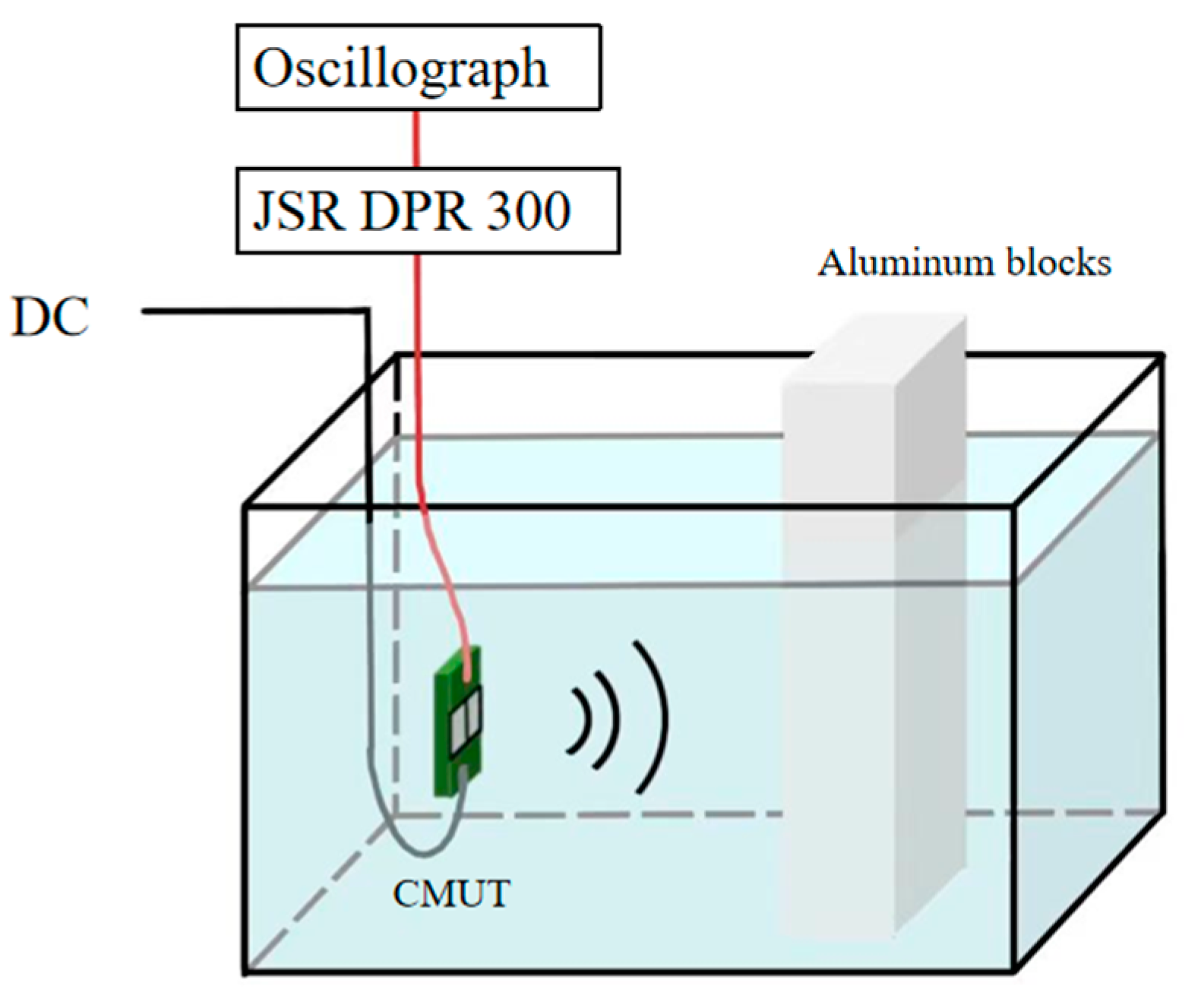
The CMUT array element was immersed in silicone oil, and its bandwidth was measured using the pulse-echo method (
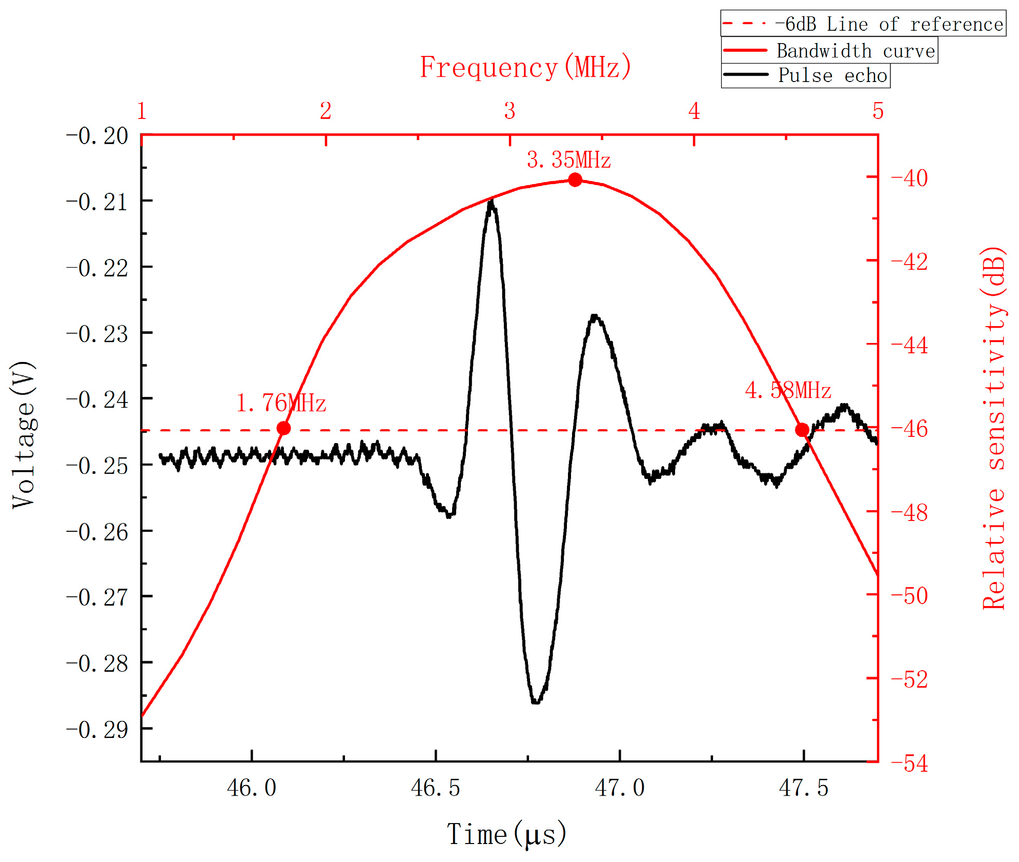
Figure 4). The JSR DPR300 ultrasonic pulse generator/receiver generated a high-voltage pulse excitation to drive the CMUT array element, which emitted ultrasonic waves. When these waves encountered the aluminum block, they were reflected to the CMUT array. The received signals were read by an oscilloscope. The Fourier transform of the received signal was used to obtain the relative sensitivity bandwidth curve of the CMUT array (
Figure 5). The packaged CMUT array exhibited a center frequency of 3.35 MHz, and a relative sensitivity fraction bandwidth of –6dB at 86%, meeting the design requirements of NDT.
3.2. Capacitance-Voltage Characteristics
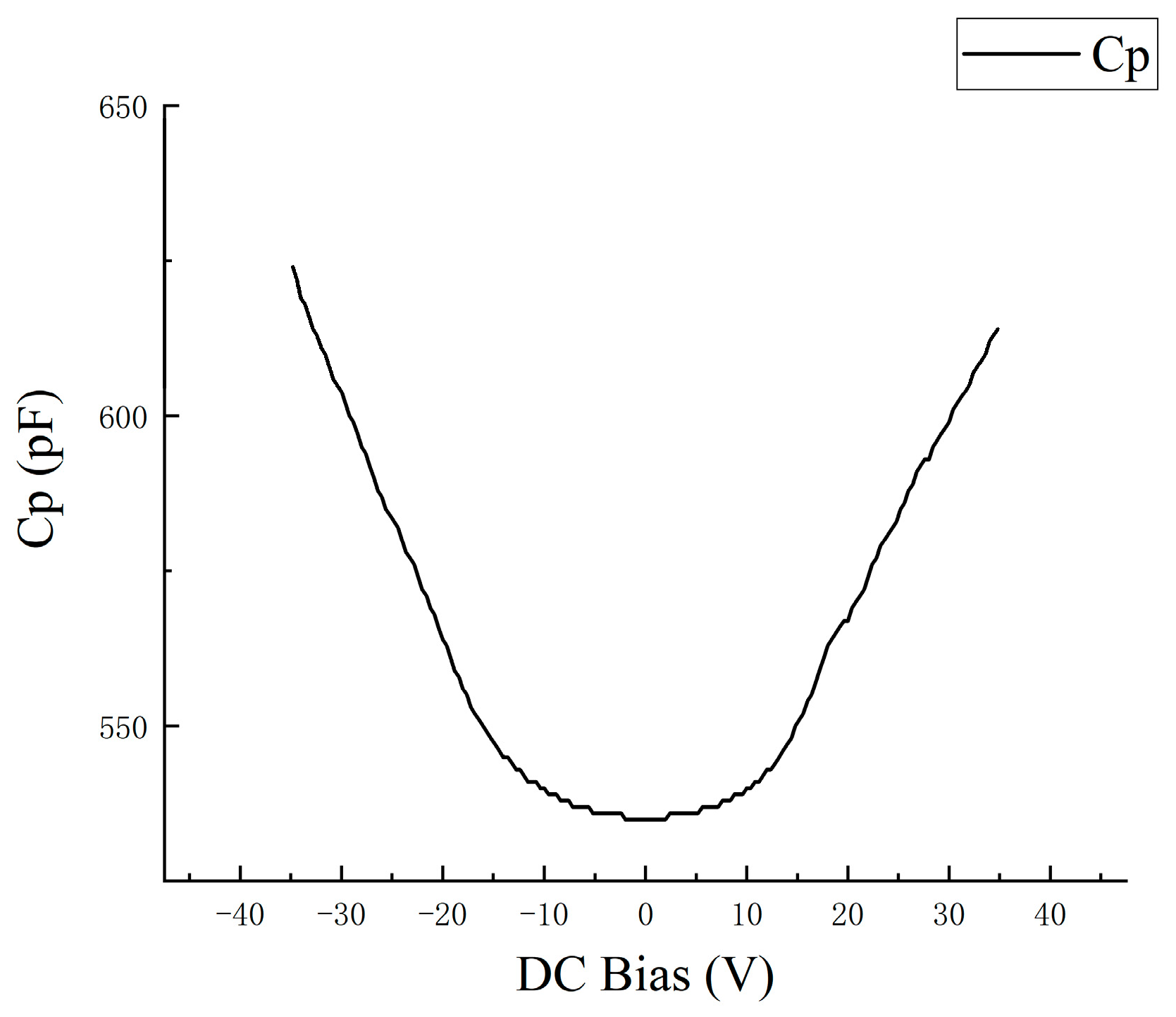
The CMUT operates based on the elastic deformation of thin capacitor plates under electrostatic force or acoustic waves. When a DC bias voltage is applied, the vibrating film of the CMUT moves towards the CMUT substrate due to electrostatic force, reducing the actual cavity thickness of CMUT and altering the CMUT’s capacitance. As the bias voltage changes, the capacitance of the CMUT also varies. The capacitance-voltage (CV) characteristics of the CMUT device illustrate the quantitative relationship between structural deformation and bias voltage. This study tested the capacitance-DC bias voltage characteristics of two CMUT arrays, as depicted in
Figure 6. The results indicate that the CMUT capacitance increased with the absolute value of DC bias voltage, which is consistent with theoretical predictions.
3.3. Reception Sensitivity Test
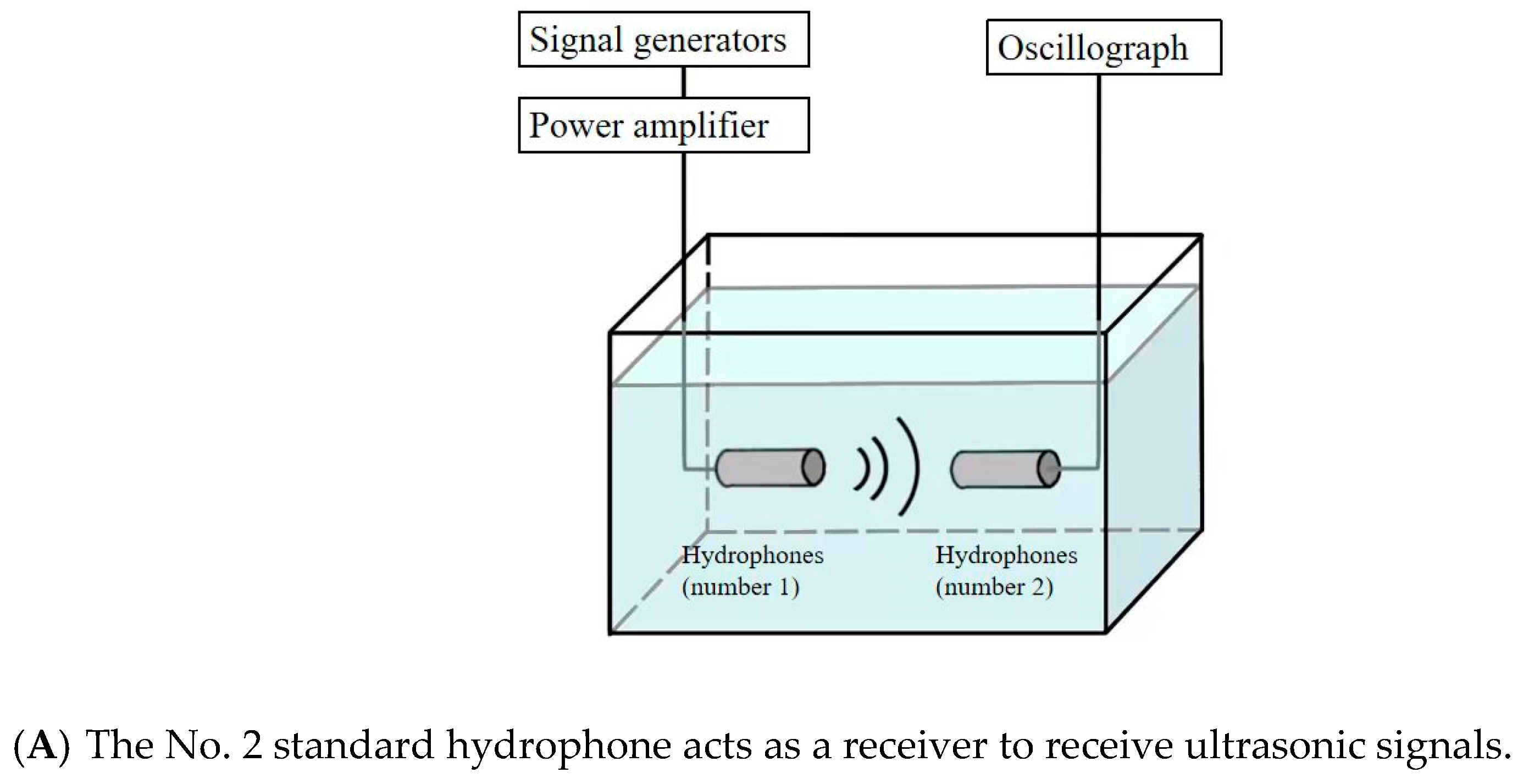
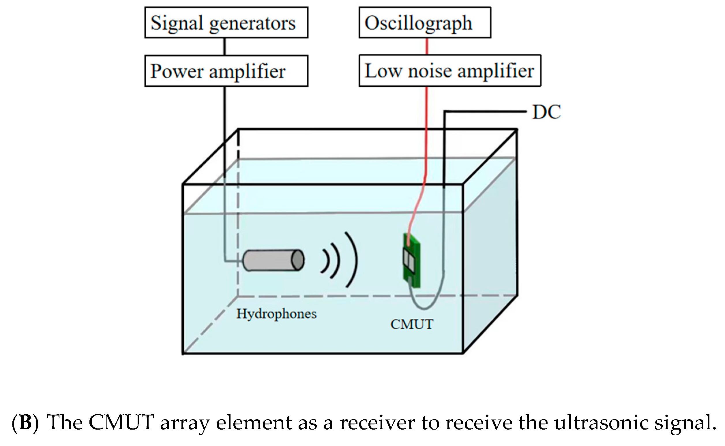
This study employed the reciprocal calibration method to assess acceptance sensitivity, as illustrated in
Figure 7. In the previous bandwidth test, the center frequency of the CMUT’s No. 1 array element was determined to be 3.35 MHz. A signal generator applied three sinusoidal pulses with a frequency of 3.4 MHz and a peak-to-peak value of 10 V to the No. 1 standard hydrophone. The No. 2 standard hydrophone, designated HPCTN-3-10-1-A-40#, served as the receiver for ultrasonic signals and was connected to an oscilloscope. The two hydrophones were spaced 10 cm apart, and the accepted voltage signal of the No. 2 standard hydrophone was recorded under these conditions. The No. 2 standard hydrophone was then substituted by two CMUT elements, each subjected to a DC voltage and an AC voltage of 20 V in turn. A low-noise amplifier with a 10x amplification was connected to the receiver, and the receiving voltage of the two CMUT elements was recorded.
Table 2 presents the peak-to-peak and acceptance sensitivity (M1/dB) of the received voltage signal at 3.4 MHz for the No. 2 standard hydrophone, along with the peak-to-peak amplitude of the received voltage signal for the two CMUT arrays. The received sensitivity (M2/dB and M3/dB) in decibels for the two CMUT elements were computed. The test results indicate that the maximum acceptance sensitivities of the two elements of CMUT in silicone oil were –197.434 dB and –197.413 dB, respectively. These demonstrate that the two elements exhibited good performance, highlighting their advantages in ultrasonic testing technology.
3.4. Metal Penetration Test
The CMUT and the aluminum block being tested were submerged in silicone oil. The CMUT emitted an ultrasonic signal under pulse excitation, and the reflected signal from the aluminum block was received by the transducer, demonstrating the CMUT’s ability to excite the signal to penetrate the aluminum block.
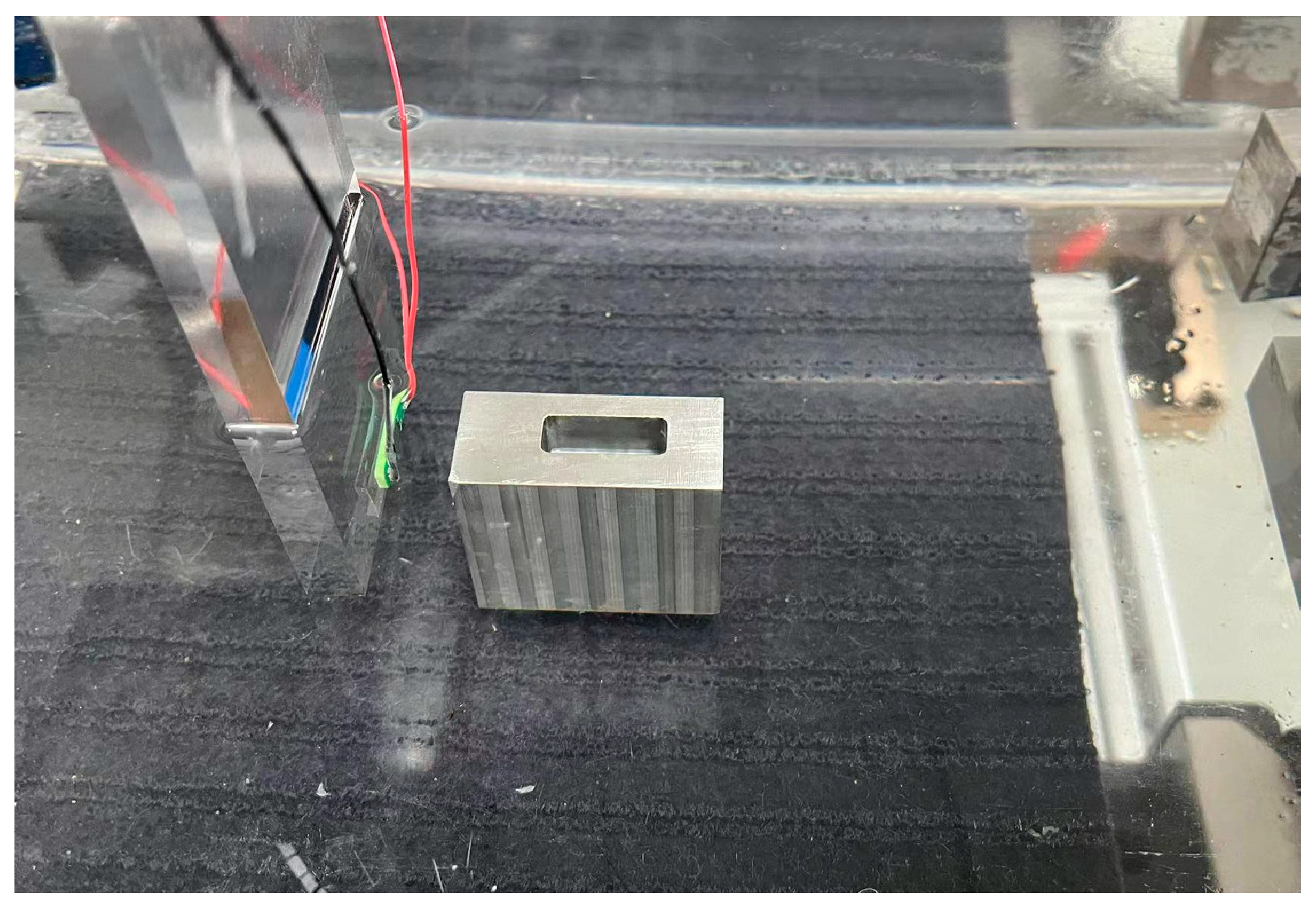
Figure 8 illustrates the actual test setup. The pulse-echo response test device comprised a pulse generation circuit, JSR DPR300, CMUT, and aluminum block. The pulse generation circuit, designed and manufactured in the laboratory, is a bipolar high-voltage pulse generator based on the MAX14808 chip, allowing for the customization of the pulse waveform, number, frequency, and duty cycle. To evaluate the CMUT's ability to detect metal defects, two aluminum blocks of identical size and material were designed, one containing a defect at a depth of 2 cm and the other intact.
In the metal penetration test, a 30 V DC bias was applied to the bottom electrode of the CMUT, while a bipolar square wave of 3.4 MHz and 40 Vpp was applied to the top electrode for five cycles using a pulse generation circuit. The square wave had a 50% duty cycle for both positive and negative polarities. The echo signal received by the CMUT was routed through a TR switch to the JSR DPR300 device, where it was filtered and amplified before being displayed on an oscilloscope. During the test, the JSR DPR300’s gain was set to 30 dB, with the cut-off frequencies of the low-pass and high-pass filters at 4.5 MHz and 1.5 MHz, respectively.
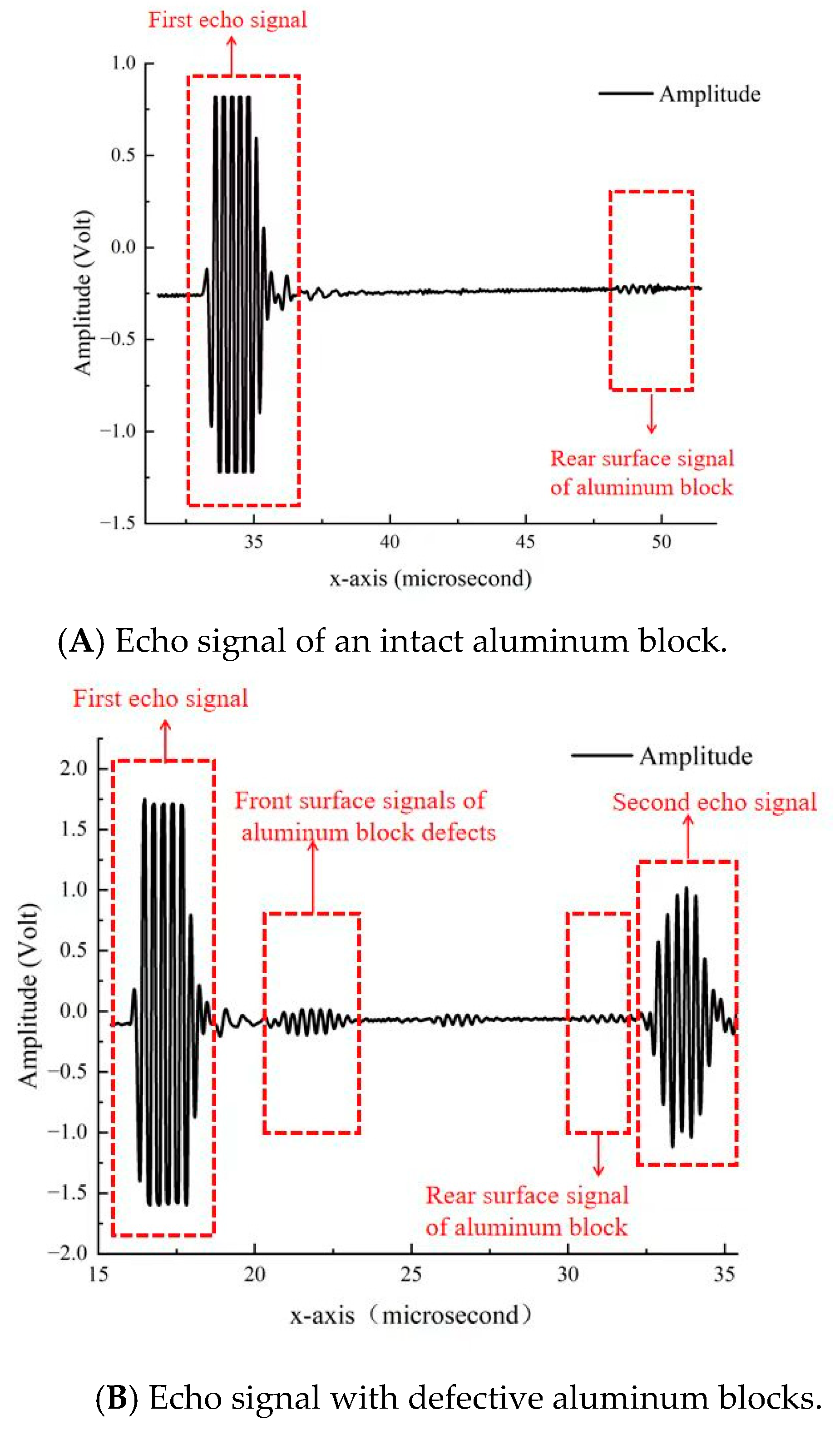
Figure 9 illustrates the experimental results of the CMUT test for metal penetration.
Figure 9a depicts the echo signals of the front and rear surfaces of the aluminum block, with no other signal in the middle. The two signals were 14.50 µs apart, and the thickness of the aluminum block was computed to be 4.57 cm, consistent with the block’s actual thickness of 4.6 cm.
Figure 9b showcases the echo signals on the front and rear surfaces of the defective aluminum block. It is observed that the signal contained defect information, and the defect depth was 1.499 cm based on the distance between the defect and echo signals on the front surface of the block. This finding is consistent with the actual 1.5 cm depth of the actual aluminum block defect.
4. Discussion
CMUTs offer advantages over PZT transducers in terms of miniaturization, high integration, and superior performance. Currently, CMUT research primarily focuses on medical imaging, with limited exploration in NDT. This study explored the potential application of the proposed CMUT device in NDT, assessing its feasibility through structural design, fabrication, and test data analysis. A CMUT device operating at 3.35 MHz was developed to meet NDT requirements. The proposed device identified defect locations by detecting ultrasonic echo signals reflected from the defective surface of an aluminum block. This study also evaluated the CV characteristics, receiving sensitivity, and bandwidth performance of the designed CMUT.
The CMUT was fabricated using silicon wafer bonding, known for its good electrical properties and high packaging density, which is advantageous for applications requiring miniaturization and integration. This process is cost-effective compared to other bonding technologies, aligning with our manufacturing needs. Future work will involve testing aluminum blocks with different defect types.
5. Conclusions
This study proposed a novel CMUT device employing silicon fusion wafer bonding technology, designed for ultrasonic transducer applications in NDT. The device’s transmit and receive sensitivities were evaluated using the reciprocity calibration approach, yielding a receiving sensitivity of –197.4 dB. The CMUT operated at a center frequency of 3.35MHz with a bandwidth of –6 dB at 86%. In metal defect testing, the sensor successfully detected and measured echo signals from metal defects, allowing for depth assessment. The performance evaluation of the proposed CMUT chip and the metal defect tests demonstrate its suitability for NDT applications.
Author Contributions
Conceptualization—Changde He, Chenyang Xue, and Wendong Zhang; methodology—Changde He, Mengke Luo, Shuaiwen Sun, Shuaiqi We, and Hanchi Chai; validation—Mengke Luo, Shuaiwen Sun, Shuaiqi We, and Hanchi Chai; formal analysis—Guojun Zhang, Renxin Wang, Jiangong Cui, Yuhua Yang, and Licheng Jia; data curation—Changde He, Mengke Luo, Shuaiwen Sun, Shuaiqi We, and Hanchi Chai; original draft preparation—Changde He, and Mengke Luo; review and editing—Guojun Zhang, Renxin Wang, Jiangong Cui, Yuhua Yang, and Licheng Jia; funding acquisition—Changde He, Chenyang Xue, and Wendong Zhang. All authors have read and agreed to the published version of the manuscript.
Funding
This research was funded by the National Key R&D Program of China (Grant number 2022YFB3205400) and the National Natural Science Foundation of China (Grant number 61927807).
Acknowledgments
We thank LetPub (
www.letpub.com.cn) for its linguistic assistance during the preparation of this manuscript.
Conflicts of Interest
The authors declare no conflicts of interest.
References
- F. Tiefensee, P. Weber, S. Kunz, M. Pamplona, and S. Simon, “Ultrasonic phased array technology for the non-destructive testing of marble sculptures,” Studies in Conservation, vol. 62, no. 1, pp. 55-60, 2017/01/02, 2017. [CrossRef]
- Y. Li, K. Yao, and X. Li, “An ultrasonic signal reconstruction algorithm of multilayer composites in non-destructive testing,” Applied Acoustics, vol. 186, pp. 108461, 2022/01/15/, 2022. [CrossRef]
- H. Nie, K. Mu, Z. Zhang, Y. Ding, S. Zhao, K. Wang, W. Dang, J. Ren, X. Liang, and W. Ma, “Preliminary study on terahertz non-destructive testing for defect detection in hot melt joints of polyethylene pipes,” Infrared Physics & Technology, vol. 139, pp. 105300, 2024/06/01/, 2024. [CrossRef]
- L. Xie, Y. Lian, F. Du, Y. Wang, and Z. Lu, “Optical methods of laser ultrasonic testing technology in the industrial and engineering applications: A review,” Optics & Laser Technology, vol. 176, pp. 110876, 2024/09/01/, 2024. [CrossRef]
- M. A. Guvenc, H. Kapusuz, and S. Mistikoglu, “Experimental study on accelerometer-based ladle slag detection in continuous casting process,” The International Journal of Advanced Manufacturing Technology, vol. 106, no. 7, pp. 2983-2993, 2020/02/01, 2020. [CrossRef]
- M. Sgarbi, V. Colla, S. Cateni, and S. Higson, “Pre-processing of data coming from a laser-EMAT system for non-destructive testing of steel slabs,” ISA Transactions, vol. 51, no. 1, pp. 181-188, 2012/01/01/, 2012. [CrossRef]
- S. Wang, F. Gan, H. Gou, and Y. Du, “An Online Monitoring Method for High- Temperature Environments Combining Eddy Current Testing and Electromagnetic Acoustic Transducer Techniques,” IEEE Sensors Journal, vol. 24, no. 6, pp. 8682-8693, 2024. [CrossRef]
- P. Ma, C. Xu, and D. Xiao, “Robotic Ultrasonic Testing Technology for Aero-Engine Blades,” Sensors, vol. 23, no. 7, pp. 3729, 2023. [CrossRef]
- F. Rubio, E. D. Blandford, and L. J. Bond, “Survey of advanced nuclear technologies for potential applications of sonoprocessing,” ULTRASONICS, vol. 71, pp. 211-222, SEP, 2016. [CrossRef]
- K. Brenner, A. S. Ergun, K. Firouzi, M. F. Rasmussen, Q. Stedman, and B. Khuri–Yakub, "Advances in Capacitive Micromachined Ultrasonic Transducers," Micromachines, 10, 2019]. [CrossRef]
- C. Goel, P.-V. Cicek, and A. Robichaud, "Design and Implementation of Low-Voltage Tunable Capacitive Micro-Machined Transducers (CMUT) for Portable Applications," Micromachines, 13, 2022]. [CrossRef]
- B. Bayram, G. G. Yaralioglu, M. Kupnik, A. S. Ergun, O. Oralkan, A. Nikoozadeh, and B. T. Khuri-Yakub, “Dynamic analysis of capacitive micromachined ultrasonic transducers,” IEEE Transactions on Ultrasonics, Ferroelectrics, and Frequency Control, vol. 52, no. 12, pp. 2270-2275, 2005. [CrossRef]
- M. Ghavami, M. R. Sobhani, and R. Zemp, “Transparent Dual-Frequency CMUT Arrays for Photoacoustic Imaging,” IEEE Transactions on Ultrasonics, Ferroelectrics, and Frequency Control, vol. 70, no. 12, pp. 1621-1630, 2023. [CrossRef]
- H. Y. Chen, Y. S. Chan, T. H. Hsu, M. H. Li, and S. S. Li, "A Single-Chip CMOS-MEMS CMUT Array Transceiver With Low Bias." pp. 136-139.
- E. F. Arkan, and F. L. Degertekin, “Analysis and Design of High-Frequency 1-D CMUT Imaging Arrays in Noncollapsed Mode,” IEEE Transactions on Ultrasonics, Ferroelectrics, and Frequency Control, vol. 66, no. 2, pp. 382-393, 2019. [CrossRef]
- M. Saccher, S. Kawasaki, J. H. Klootwijk, R. V. Schaijk, and R. Dekker, “Modeling and Characterization of Pre-Charged Collapse-Mode CMUTs,” IEEE Open Journal of Ultrasonics, Ferroelectrics, and Frequency Control, vol. 3, pp. 14-28, 2023. [CrossRef]
- J. Chen, “Capacitive micromachined ultrasonic transducer arrays for minimally invasive medical ultrasound,” Journal of Micromechanics and Microengineering, vol. 20, no. 2, pp. 023001, 2010/01/29, 2010. [CrossRef]
- S. H.-L. Tu, and P.-Y. Tsai, “A Class-E high-voltage pulse generator for ultrasound medical imaging applications,” Microelectronics Journal, vol. 100, pp. 104776, 2020/06/01/, 2020. [CrossRef]
- M. Annayev, T. I. Minhaj, O. J. Adelegan, F. Y. Yamaner, P. A. Dayton, and O. Ö, “Design and Fabrication of 1-D CMUT Arrays for Dual-Mode Dual-Frequency Acoustic Angiography Applications,” IEEE Transactions on Ultrasonics, Ferroelectrics, and Frequency Control, vol. 71, no. 1, pp. 191-201, 2024. [CrossRef]
- P. Ramm, J. J.-Q. Lu, and M. M. V. Taklo, Handbook of Wafer Bonding: Wiley-VCH, 2012.
|
Disclaimer/Publisher’s Note: The statements, opinions and data contained in all publications are solely those of the individual author(s) and contributor(s) and not of MDPI and/or the editor(s). MDPI and/or the editor(s) disclaim responsibility for any injury to people or property resulting from any ideas, methods, instructions or products referred to in the content. |
© 2024 by the authors. Licensee MDPI, Basel, Switzerland. This article is an open access article distributed under the terms and conditions of the Creative Commons Attribution (CC BY) license (http://creativecommons.org/licenses/by/4.0/).
