1. Introduction
Yttrium ferrite (YFeO
3, YFO) thin films have garnered significant attention in the scientific community due to their unique and valuable properties. Yttrium ferrite thin films exhibit excellent magnetic properties, including high coercivity and remanence, making them suitable for various magnetic applications [
1]. These films can be engineered to have specific magnetic characteristics, useful in magnetic storage devices, spintronics, and magnetic sensors [
2]. Yttrium ferrite belongs to the class of multiferroic materials, which exhibit more than one ferroic order parameter (ferromagnetism, ferroelectricity, or ferroelasticity) simultaneously [
3]. This dual functionality is highly beneficial for advanced electronic devices, allowing for the development of components that can be controlled by both electric and magnetic fields [
4]. In microelectronics, yttrium ferrite thin films are used for their dielectric properties. Their high dielectric constant and low loss tangent make them suitable for capacitors and other electronic components where minimizing energy loss is crucial [
5]. Yttrium ferrite thin films are also explored for energy storage and conversion applications [
6]. Their ability to maintain stable performance under varying environmental conditions is advantageous for batteries, supercapacitors, and fuel cells [
7]. The chemical stability of yttrium ferrite thin films is another important characteristic, making them suitable for harsh environments where other materials might degrade [
8]. This stability is beneficial for coatings, sensors, and other applications requiring long-term reliability [
9].
The optical properties of yttrium ferrite thin films, such as their band gap and refractive index, can be tailored through thin film fabrication techniques. This tunability makes them suitable for optoelectronic applications, including photodetectors, photovoltaics, and light-emitting devices [
10,
11]. One of the primary optical properties of yttrium ferrite thin films is their band gap. The band gap of YFO is a critical parameter that defines its electronic and optical behavior. Typically, the band gap of yttrium ferrite thin films is in the range of 2.0 to 2.2 eV . This makes them suitable for applications in visible light photodetection and photovoltaic devices. The direct band gap nature facilitates efficient electron transition from the valence band to the conduction band upon light absorption, making YFO thin films efficient light absorbers.
The refractive index (n) of yttrium ferrite thin films is another crucial optical parameter. It typically ranges from 2.2 to 2.6 at visible wavelengths. This high refractive index indicates strong interaction with visible light, which is advantageous for applications in optical coatings and waveguides. The dielectric function, which encompasses both the real (ε1) and imaginary (ε2) parts of the dielectric constant, provides further insights into the material’s optical response. The real part of the dielectric function relates to the material’s ability to store electrical energy, while the imaginary part corresponds to energy dissipation. For yttrium ferrite, ε1 generally shows a value around 5-6 in the visible range, while ε2 can vary depending on the specific wavelength and film processing conditions [
12].
Yttrium ferrite thin films also exhibit notable optical conductivity. Optical conductivity is a measure of a material’s ability to conduct electric current under the influence of an optical field. For YFO thin films, the optical conductivity can be significant in the visible region, contributing to their potential use in optoelectronic devices [
13]. Despite their ability to absorb and conduct light, these films maintain a degree of transparency, particularly in the near-infrared region, which is beneficial for applications requiring both conductivity and transparency, such as in transparent electrodes for display technologies [
14].
Photoluminescence (PL) is another critical optical property of yttrium ferrite thin films. Under excitation, these films can exhibit strong photoluminescence, typically peaking in the visible spectrum. The PL intensity and peak position can be influenced by factors such as film thickness, crystallinity, and the presence of defects or impurities. This property is particularly valuable for applications in light-emitting devices and sensors. Additionally, yttrium ferrite thin films possess nonlinear optical properties, which are essential for applications in advanced photonic devices [
15]. Nonlinear optical behavior such as second-harmonic generation has been observed in these films, indicating their potential in frequency doubling applications and in the development of photonic circuits [
16].
The optical properties of yttrium ferrite thin films can be finely tuned through various doping strategies and fabrication techniques [
17]. For instance, doping with elements such as titanium (Ti) or cobalt (Co) can modify the band gap, refractive index, and photoluminescence characteristics. Advanced fabrication techniques such as pulsed laser deposition (PLD), sputtering, and sol-gel methods allow precise control over film thickness, crystallinity, and surface morphology, further influencing the optical properties [
12]. For example, PLD can produce highly crystalline films with smooth surfaces, which are crucial for minimizing scattering losses in optical applications [
18].
While the current literature YFO thin films has provided significant insights into their optical properties and potential applications in spintronics and photonics, several critical gaps remain that hinder a comprehensive understanding and broader application of these materials. Existing studies often lack a detailed characterization of the full spectrum of optical properties. Specific measurements of the band gap, absorption coefficients, refractive index, and dielectric constants across a range of wavelengths are not consistently reported. This incomplete data hampers the ability to tailor these materials for precise optoelectronic applications. The literature frequently mentions the fabrication of Yttrium Orthoferrite thin films using various deposition techniques such as plasma laser deposition, sputtering, and sol-gel methods. However, systematic studies on how different deposition parameters—such as substrate temperature, ambient pressure, and laser energy—affect the structural and optical properties of the films are scarce. Understanding these relationships is crucial for optimizing the fabrication process.
This paper systematically examines the influence of deposition time on the quality and optical properties of the thin films. This aspect is particularly novel as it provides detailed insights into how varying the deposition duration can affect the topography, composition and optical performance of the films. Such a systematic study helps in optimizing deposition parameters to achieve the desired film characteristics, which is critical for both fundamental research and practical applications. The pioneering data and interdisciplinary approach presented in this study make it a significant addition to the field of coating technology and materials science. The paper suggests that the optimized deposition conditions can lead to YFO thin films with superior optical properties. This potential for enhanced material performance opens new avenues for the practical use of these films in advanced optoelectronic devices, offering significant improvements over existing materials.
2. Materials and Methods
Yttrium orthoferrite thin films with different thicknesses were deposited on cleaned silicon (Si) substrates (525 ± 25 μm thick). The deposition process was carried out at a temperature of 723.15 °K using a pulsed laser deposition system (TSST, Strasbourg, France), with a sintered ceramic pellet of the orthorhombic YFO serving as the PLD target. Prior to deposition, the Si substrates underwent a thorough cleaning procedure. They were initially immersed in a hydrofluoric acid (HF) solution for a duration of 10 minutes. Subsequently, the substrates were sequentially immersed in high-purity ethanol and distilled water for 10 minutes each. These meticulously cleaned substrates were then rinsed extensively with distilled water and stored until further use. Just before the film deposition, the Si substrates were thoroughly dried under nitrogen gas. Afterwards, for the depositions, the fabrication of YFO thin films on Si substrates was carried out using a KrF excimer laser with a wavelength of 248 nm. The deposition was performed at a laser energy density of 2 J/cm
2 and a repetition rate of 5 Hz. Throughout the deposition process, the substrate temperature was held at 723.15 °K in an oxygen ambience of 1.3e
-2 mbar. A series of three separate deposition processes were executed, with all deposition parameters held constant. The control of film thickness was achieved by adjusting the number of laser pulses employed for ablating YFO nanoparticles from the bulk YFO target. Specifically, three different film thicknesses were fabricated, corresponding to 7000, 9000, and 12000 laser pulses. A detailed summary of the deposition parameters for the YFO thin films can be found in
Table 1.
Atomic force microscopy (AFM) was used to investigate the surface topography in contact mode using an NTegra Prima system (Spectrum Instruments, Russia) and a CSG01 probe with a tip diameter of 6 nm. In contact mode, the AFM probe maintains continuous contact with the sample surface as it scans, allowing for high-resolution imaging. The interactions between the probe tip and the surface cause deflections in the flexible cantilever, which are detected by a laser beam reflected onto a position-sensitive photodetector. These deflections are converted into detailed topographical data, providing precise surface characterization at the nanoscale.
Ellipsometric measurements were carried out using a spectroscopic ellipsometer (J.A. Woollam Co., Inc., VASE - Variable Angle Spectroscopic Ellipsometer). The instrument was equipped with a monochromatic light source capable of producing a broad spectrum of wavelengths (e.g., 190 nm to 1000 nm) and a rotating analyzer configuration. Measurements were taken at 60° and 80° angles of incidence. The angle range was chosen to ensure sufficient sensitivity to both the film thickness and optical properties. For each angle of incidence, the ellipsometric parameters Ψ (Psi) and Δ (Delta) were recorded across the selected wavelength range. Ψ represents the amplitude ratio, and Δ represents the phase difference between the p- and s-polarized light components upon reflection. The optical constants (refractive index, n and extinction coefficient, k were extracted by fitting the experimental data to the theoretical model using regression analysis. The fitting process was performed using the software provided with the ellipsometer (WVASE32).
X-ray photoelectron spectroscopy (XPS) measurements were conducted using an AXIS Supra XPS system (Kratos Analytical Ltd., Manchester, UK). This system is equipped with a monochromatic Al Kα X-ray source (1486.6 eV) and a hemispherical energy analyzer, providing high-resolution and high-sensitivity surface chemical analysis. Samples were mounted on the sample holder using conductive copper tape to ensure good electrical contact and minimize charging effects during measurement. The measurement were carried out in ultra-high vacuum conditions (< 10-9 mbar). The XPS spectra were acquired using the Al Kα X-ray source, operated at 150 W power (15 kV, 10 mA). Survey scans were performed over the binding energy range of 0 to 1200 eV to identify the elemental composition of the YFeO3 films. High-resolution scans were acquired for the core-level regions of Y 3d, Fe 2p, and O 1s to obtain detailed chemical state information. The pass energy for survey and high-resolution scans was set to 80 eV and 20 eV, respectively. The acquired spectra were processed using the CasaXPS software (version 2.3.23, Kratos Analytical Ltd., Manchester, UK) using Gaussian-Lorentzian. Background subtraction was performed using the Shirley method to remove inelastic scattering contributions.
Raman spectroscopy measurements were performed using a WITec alpha300 R Raman microscope (WITec, Ulm, Germany). The system was equipped with a high-resolution CCD detector and a monochromatic laser source with an excitation wavelength of 532 nm. The laser power was set to 20 mW to ensure optimal signal intensity while avoiding sample damage. The Raman microscope was calibrated using a silicon standard to ensure the accuracy of the Raman shift measurements. The characteristic Si peak at 520.7 cm⁻¹ was used for this calibration. The obtained Raman spectra were processed using WITec Project software. PL spectra were recorded using the same 355 nm laser excitation at 4 mW power. The spectral range for PL measurements was typically from 400 nm to 800 nm, depending on the expected emission wavelengths of the YFeO3 films. Number of accumulations for Raman spectra were 50 and integration time 10s. Similar to the Raman measurements, the PL signal was accumulated over 5 scans with an integration time of 25 seconds per scan to improve the signal-to-noise ratio and ensure reliable data.
Reflectance measurements and band gap determination were performed using a JASCO V-670 UV-Vis-NIR spectrophotometer (JASCO International Co., Ltd., Tokyo, Japan). The instrument is equipped with a dual-grating monochromator, allowing high-resolution measurements across a broad spectral range from 190 nm to 2700 nm. The spectrophotometer was also configured with an integrating sphere attachment to accurately measure diffuse and specular reflectance. The spectrophotometer was calibrated using a certified reflectance standard (calibrated white standard). This step ensured the accuracy and reproducibility of the reflectance measurements. The reflectance data were processed using the JASCO Spectra Manager software. Baseline correction (using spectralon material) was applied to account for any instrumental background.
3. Results
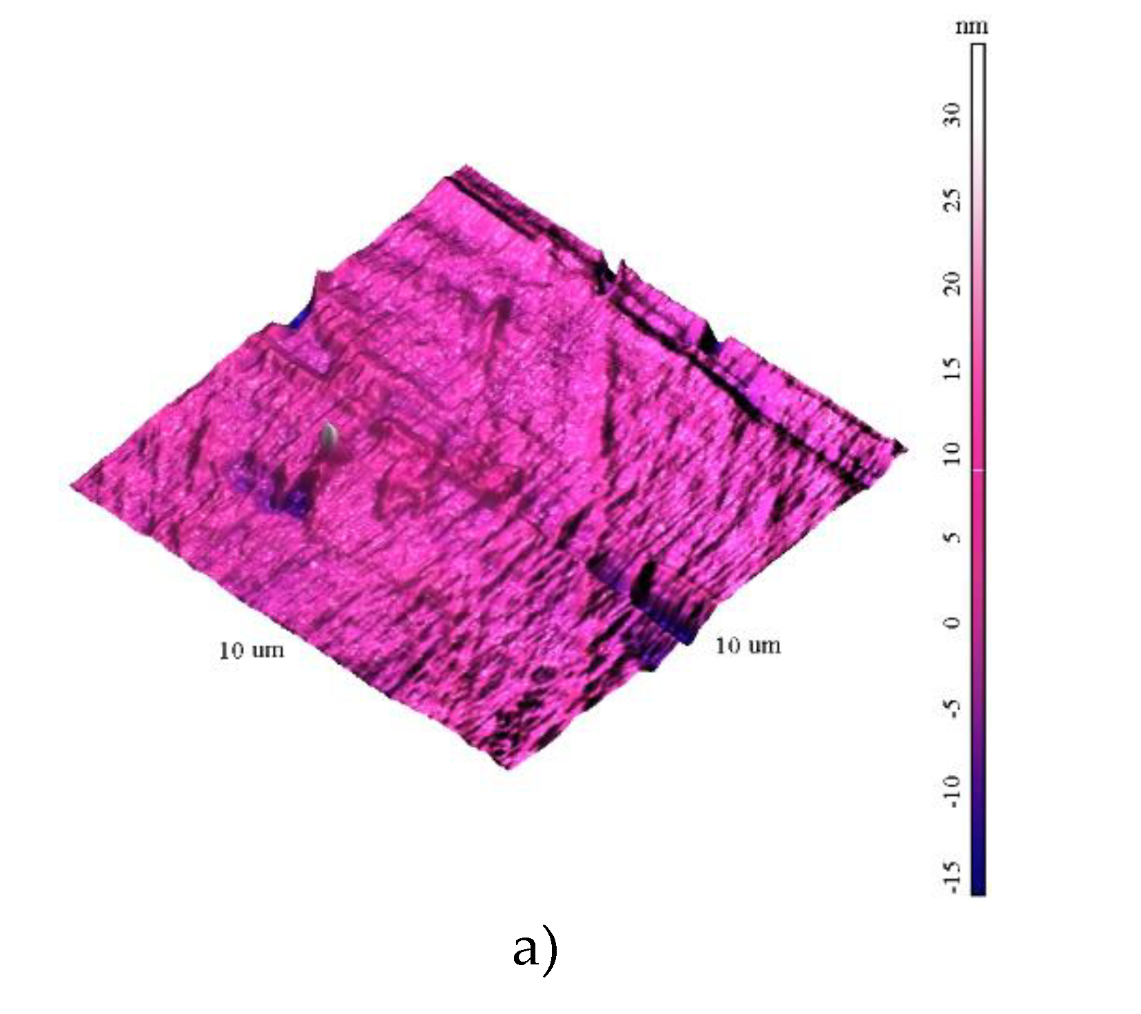
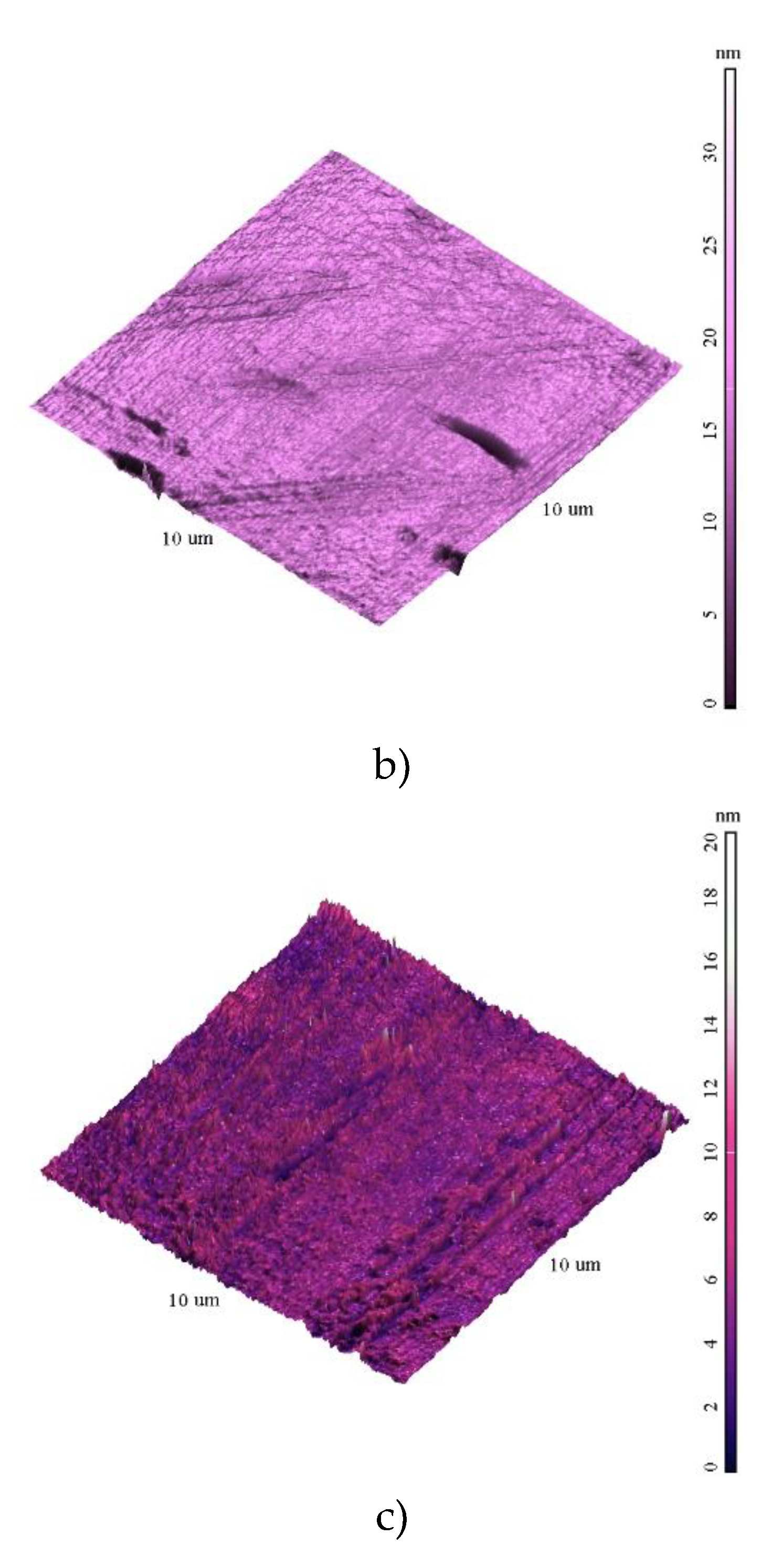
The surface exhibited non-uniform topography, with variations in height up to 35 nm. The data are presented in supplementary file S1 in common format of scanning probe microscopy files. The presence of surface defects such as pits, cracks, or inclusions was identified. Comparisons with of the samples shows that the roughness decreases with the growth of film, which covers the defects of the silicon substrates (the source of the surface inhomogeneities).
Figure 1.
AFM images of the films surfaces 10x10 µm a) S1; b) S2; c) S3.
Figure 1.
AFM images of the films surfaces 10x10 µm a) S1; b) S2; c) S3.
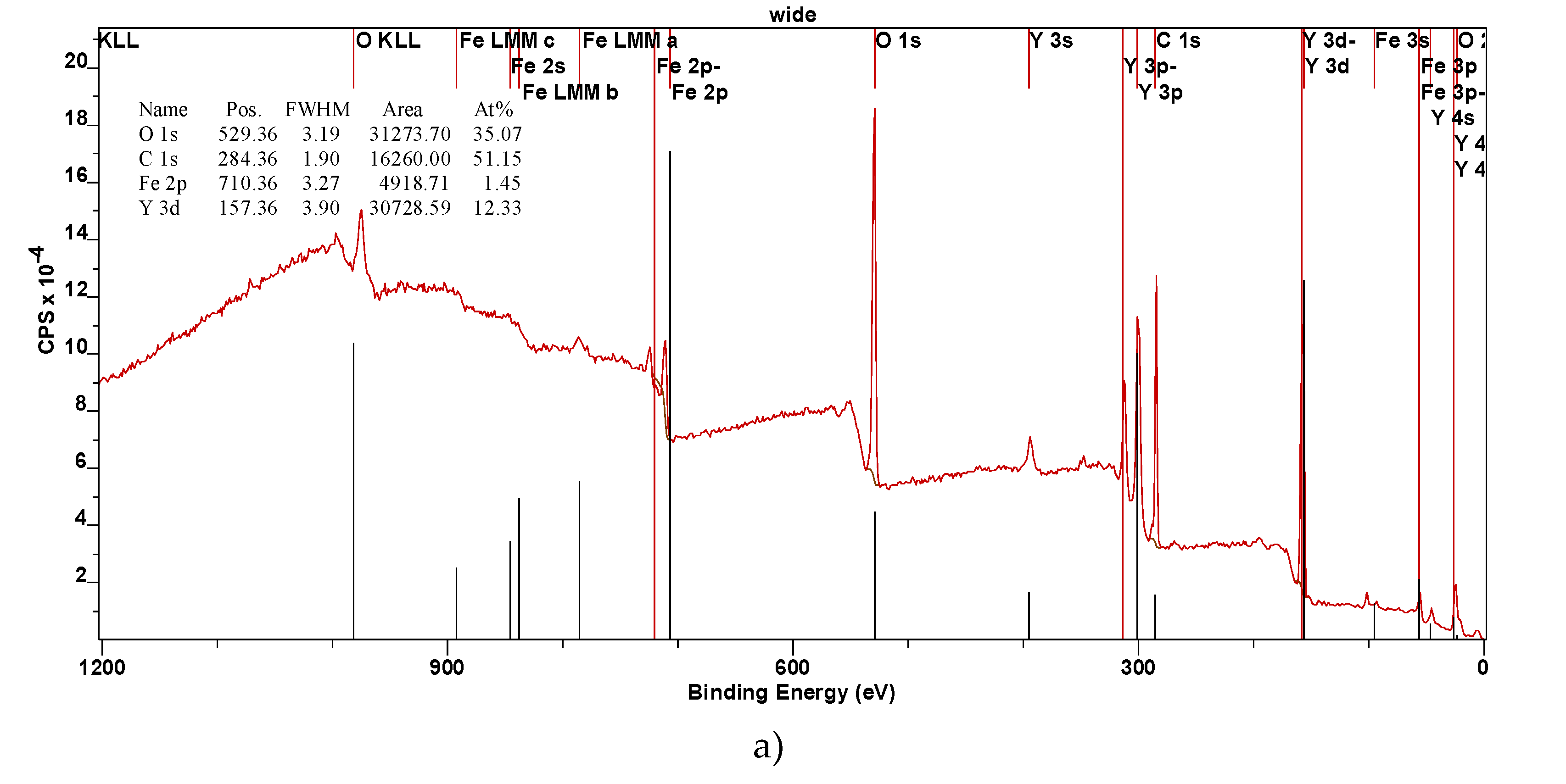
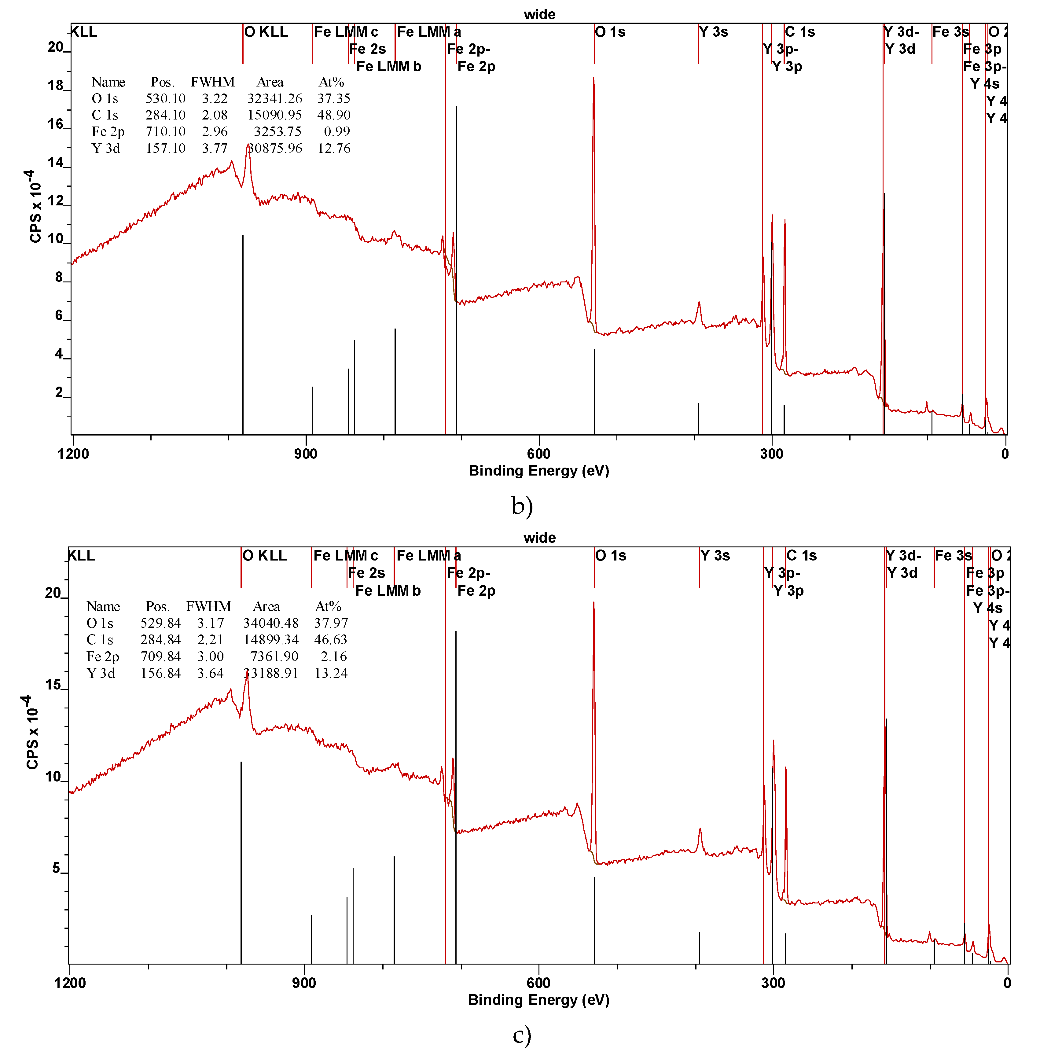
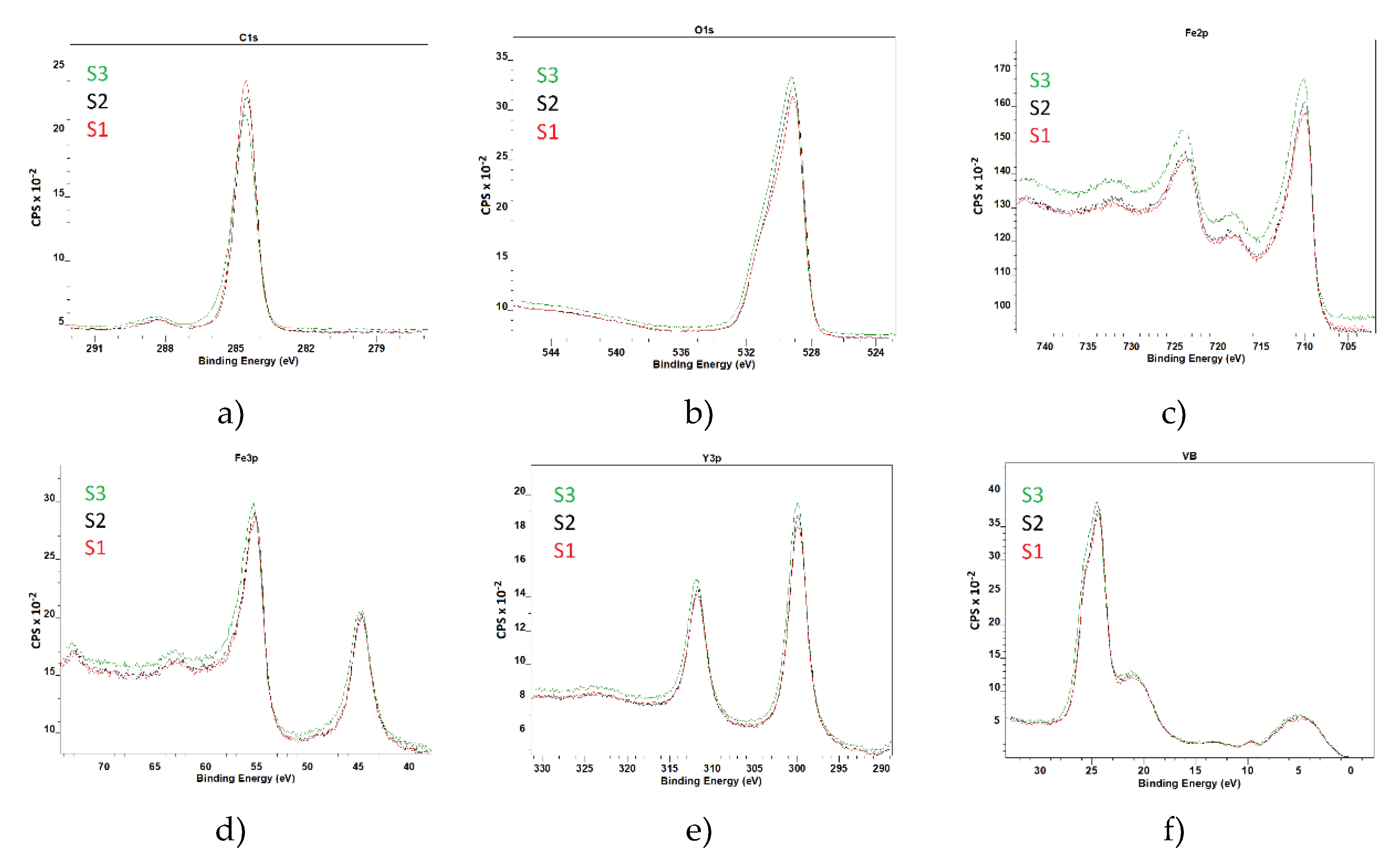
The XPS spectra were calibrated using the C 1s peak at 284.6 eV as a reference to ensure accurate binding energy measurements. This contamination is commonly observed in XPS measurements due to exposure to air. If necessary, the carbon contamination can be reduced or eliminated by annealing the samples in a high vacuum environment. The survey spectra, as shown in
Figure 2, confirm the presence of iron (Fe), yttrium (Y), and oxygen (O) in the YFeO
3 films. The identification of these elements is consistent with the expected stoichiometry of the YFeO
3 compound. The detailed spectra of each element are presented in
Figure 3.
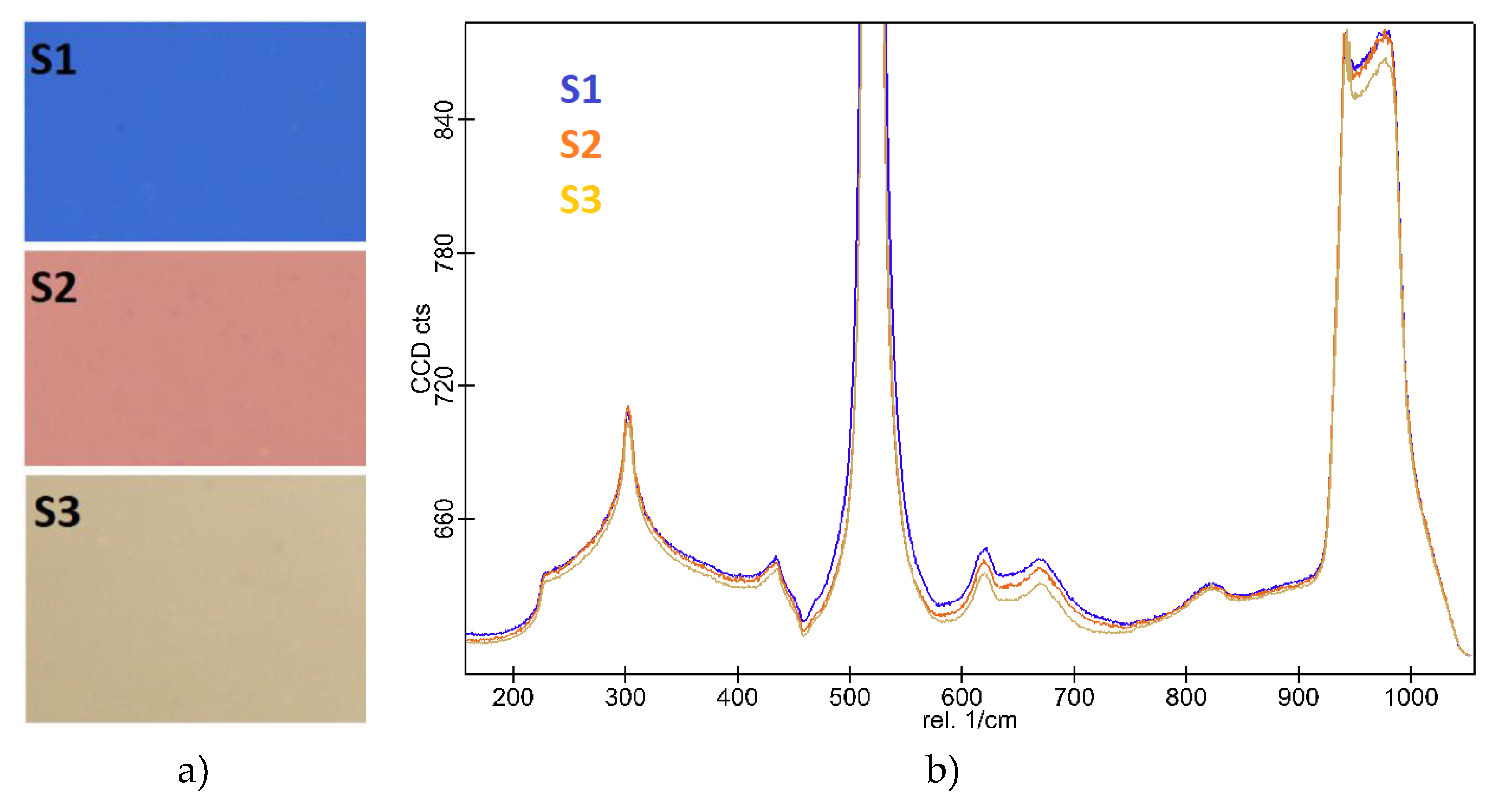
The high magnification (100x) objective enabled precise focusing and collection of Raman signals from specific areas of the film, enhancing the detection of subtle structural features (
Figure 4b). To visually assess the homogeneity of the YFeO3 films, an optical image of the sample was taken using a lower magnification objective lens, as shown in
Figure 4a. This image provides an overview of a larger area of the film, highlighting its uniformity and consistency in real colors. The lower magnification image ensures that any macroscopic inhomogeneities or defects are clearly visible, thus supporting the comprehensive analysis of film quality.
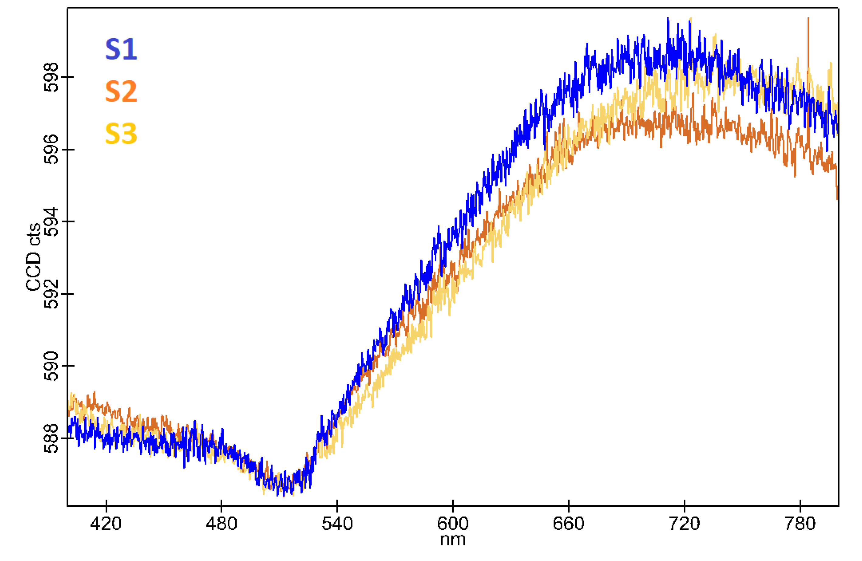
The PL spectra were acquired using a UV laser with a magnification 40x objective lens, which provided a balance between spatial resolution and area coverage, ensuring detailed yet comprehensive analysis of the film’s luminescent properties. To enhance the clarity and readability of the PL spectra, the raw data were processed using an averaging filter. This smoothing process helped to reduce noise and improve the signal-to-noise ratio, resulting in clearer and more interpretable spectral features (
Figure 5).
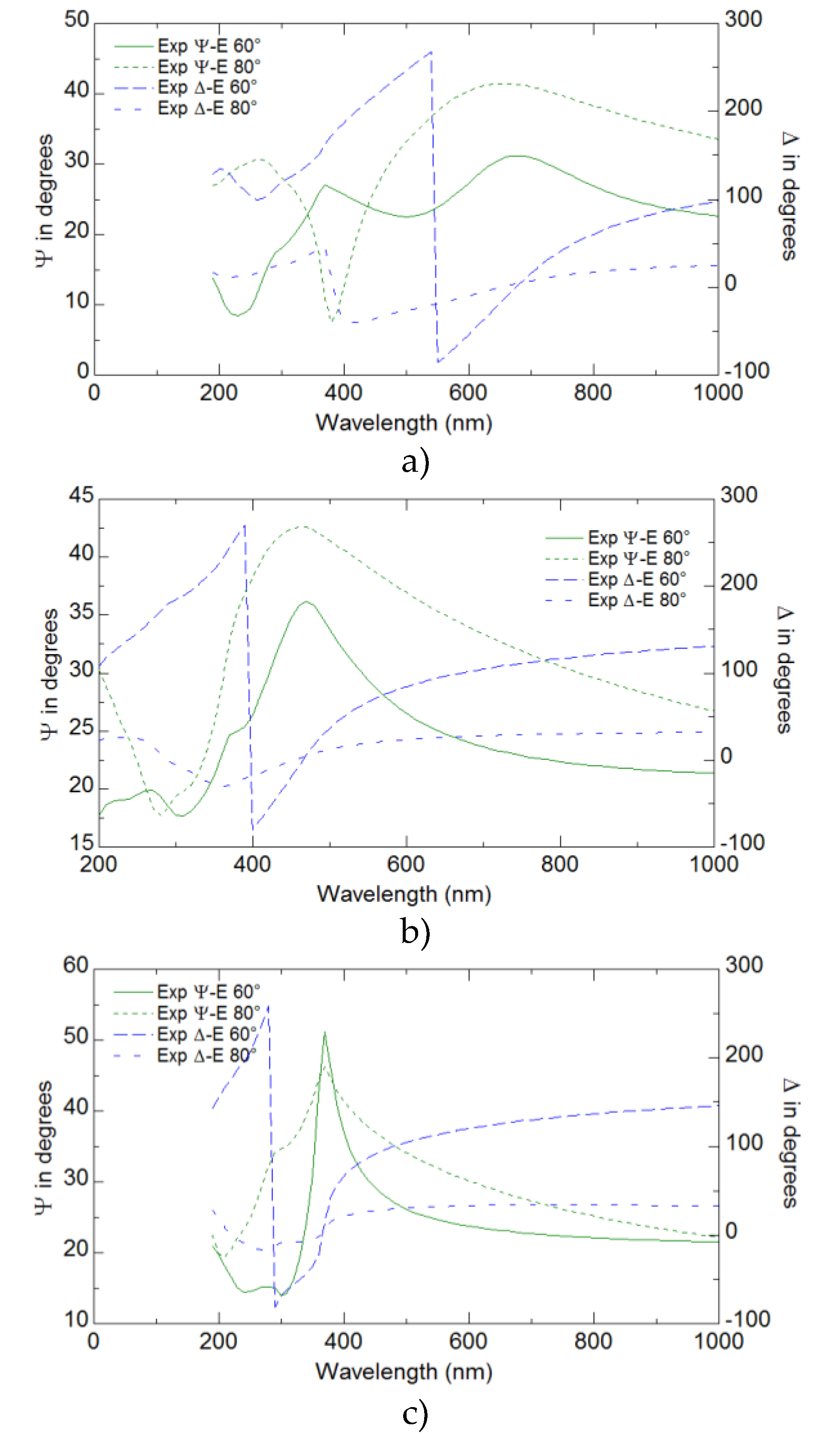
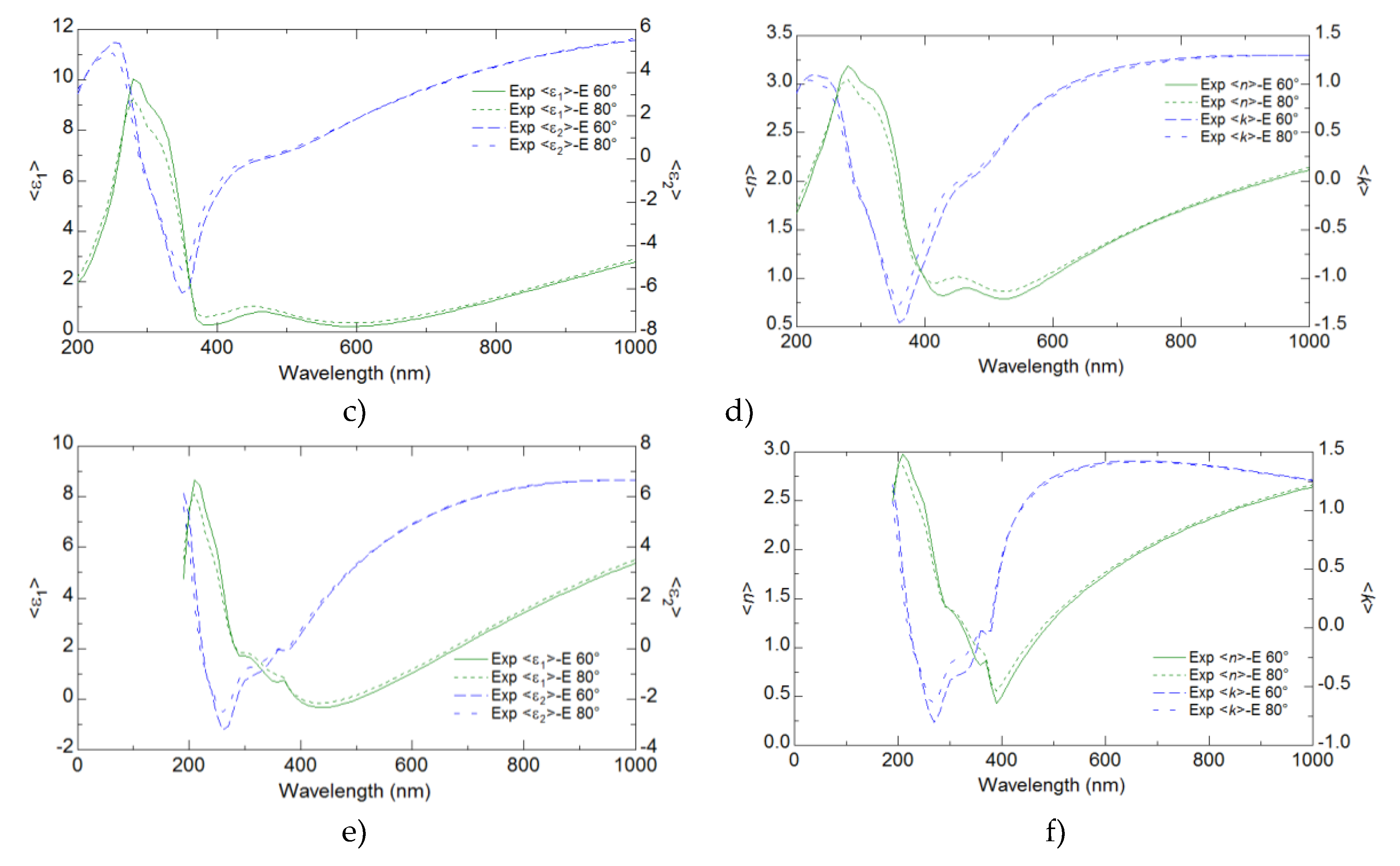
Ellipsometry provided detailed insights into the optical properties of the YFeO
3 films, revealing key parameters such as the refractive index, extinction coefficient, and dielectric functions. These optical properties were found to have a significant correlation with the electrical performance of the films. The analysis demonstrated that regions with higher refractive indices and dielectric functions corresponded to improved electrical conductivity and mobility (
Figure 6 and
Figure 7).
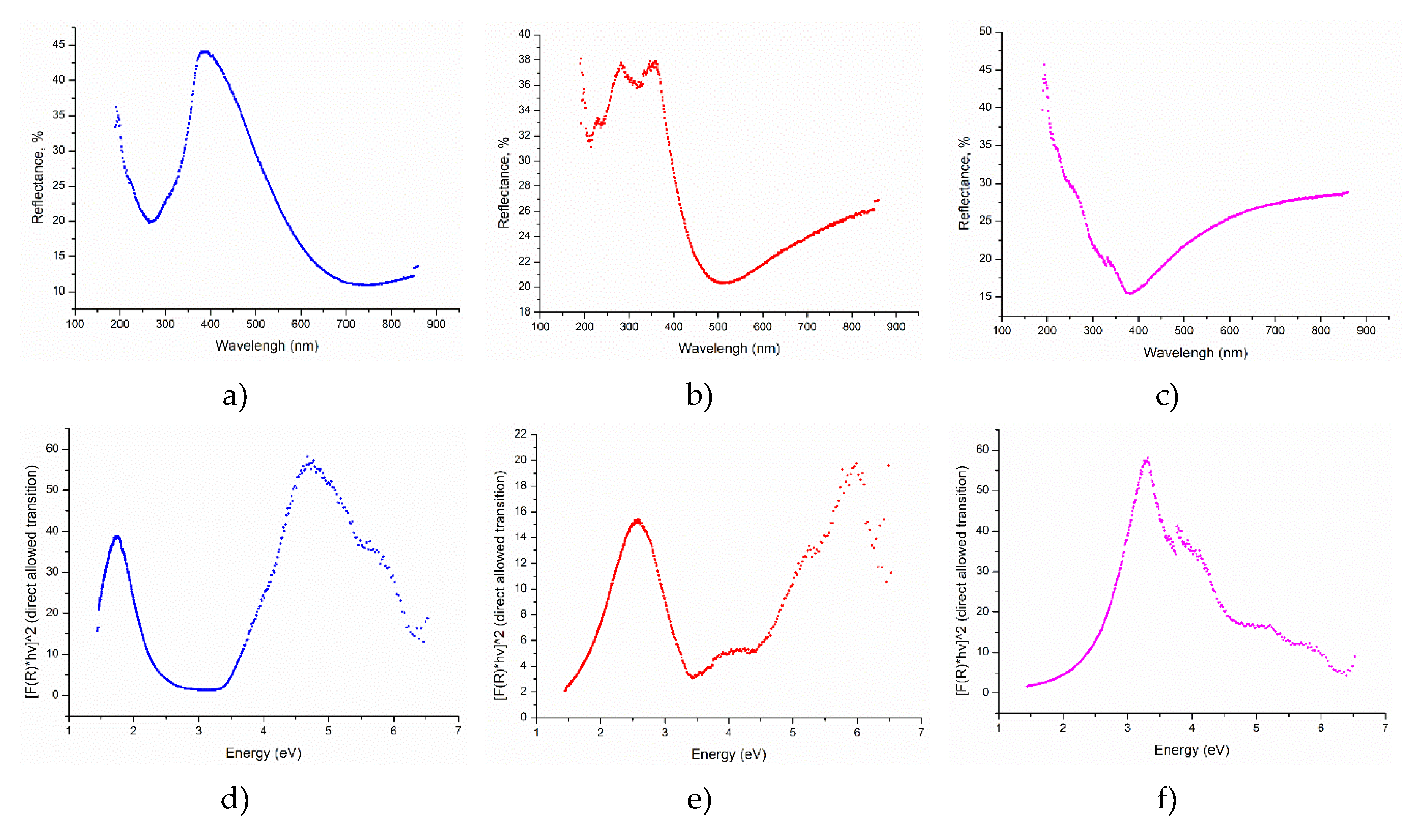
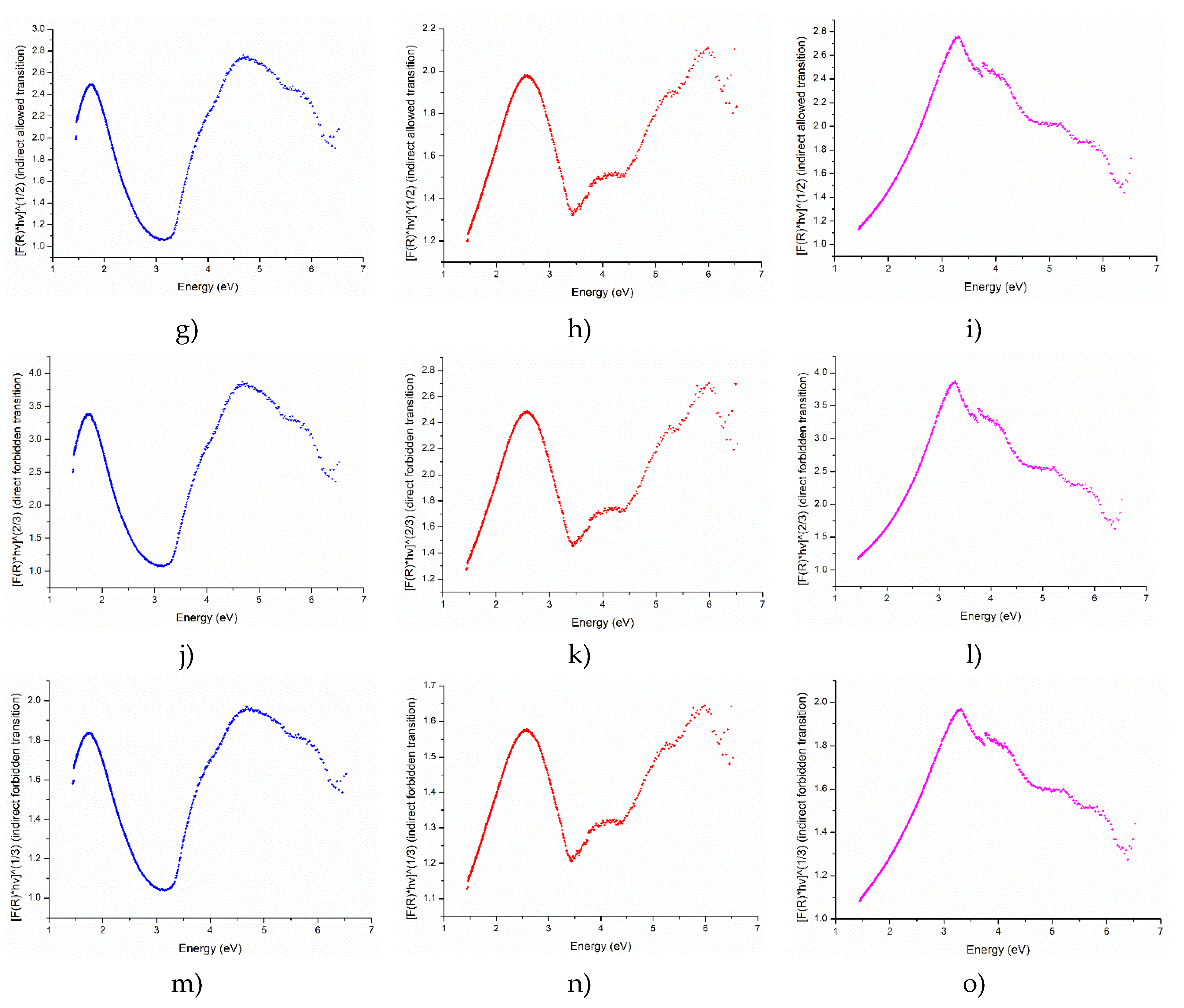
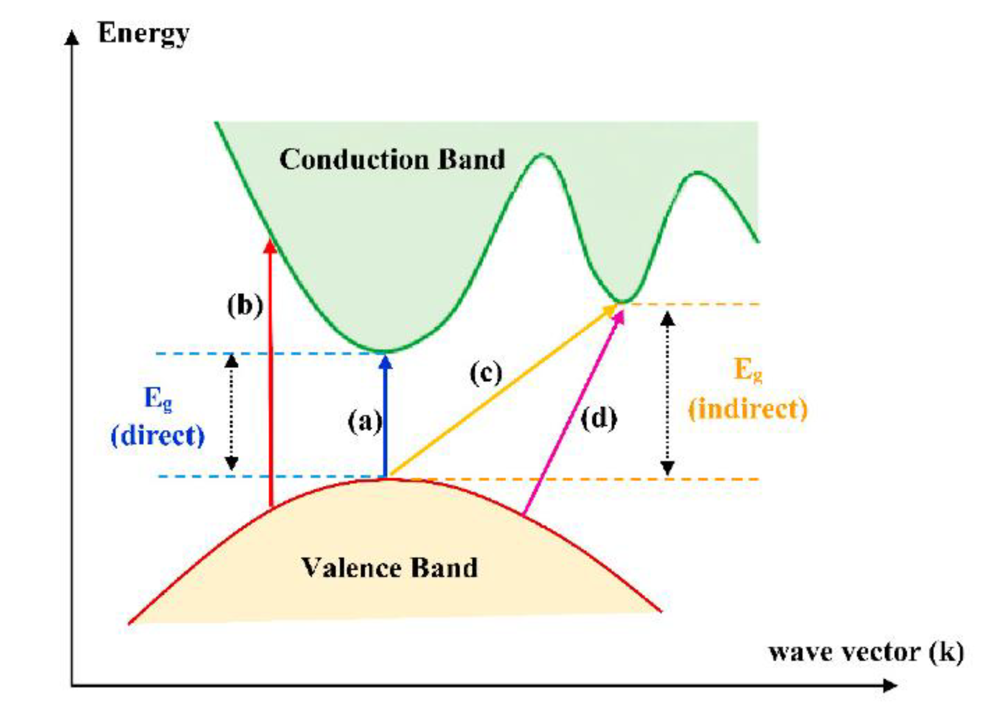
Reflectance measurements were conducted to determine the optical band gap, Urbach energy, and the nature of electronic transitions (direct/indirect and allowed/forbidden) in the YFO films. These optical parameters provide crucial insights into the electronic structure and optical properties of the material. The optical band gap is determined using Tauc plots derived from the reflectance data. The absorption coefficient was calculated using the Kubelka-Munk function. Detailed calculation is given in the supplementary material S5 (
Figure 8).
4. Discussion
The analysis of the YFO films revealed several key insights regarding their morphology, elemental composition, and electronic structure. The smoothest morphology was observed for the film labeled S3, which effectively covered the defects present on the silicon substrates. This indicates that the deposition process for S3 resulted in a more uniform and defect-free film surface, enhancing its overall quality and potential performance in applications requiring smooth, continuous films (
Figure 1 and ). The XPS wide spectra provided valuable information about the elemental composition of the films. The data showed that the amount of yttrium increased with the number of deposition pulses, indicating successful incorporation of yttrium into the film structure as deposition progressed. A slight increase in the oxygen O1s peak was also observed, consistent with the formation of YFO, which requires oxygen for its stoichiometric balance. Given the surface sensitivity of XPS, a significant C1s peak was detected (
Figure 2). However, this peak is attributed to adventitious carbon contamination from the environment and is not part of the intrinsic film structure. Notably, the S3 sample exhibited a lower carbon content, likely due to its smoother and less developed morphology, which reduces surface area available for contamination. The Fe 2p peak intensity was higher for the S3 film, and this was corroborated by additional Fe 3p scans. The Y 3p signal was also more pronounced, further confirming the increased presence of these elements in the S3 film (
Figure 3). The observation that the valence band position is unchanged implies that the differences in the electronic structure among the samples are due to variations in the conduction band position and defect states within the band gap. These findings are crucial for understanding the electronic behavior of the films and for optimizing their properties for specific applications, such as optoelectronics or photovoltaics (Supplementary 2).
The optical photographs of the films reveal their real colors, indicating that the optical properties of the films are indeed influenced by the number of deposition pulses, which in turn correlates with film thickness. As the number of pulses increases, the films become thicker, leading to changes in their color and optical behavior. This relationship highlights the importance of controlling deposition parameters to tailor the optical properties of the films for specific applications. The Raman spectroscopy results did not prominently show the presence of the YFO films due to the laser’s penetration depth being greater than the film thickness. Consequently, the spectra were dominated by a very intense peak from the silicon substrate, which matched perfectly with the characteristic Raman signal of silicon. The YFO Raman fingerprints were very weak and not clearly observable. However, for the S3 sample, which is supposed to be thicker, there was a slight shading of the silicon signal, suggesting that the thicker film partially attenuated the substrate’s Raman signal. This observation confirms that the film thickness affects the detectability of the film’s Raman signal, with thicker films offering better coverage and potentially more pronounced signals (
Figure 4). The PL spectra provided additional insights into the optical properties of the films. The S1 sample exhibited higher PL intensity, which can be attributed to unresolved mechanical stress within the film. This stress can lead to an increase in PL emission, indicating that the mechanical properties of the films significantly influence their optical behavior. The higher PL intensity in the S1 sample suggests that the thinner films are more prone to stress, which can enhance luminescence (
Figure 5, Supplementary 3).
The results from the ellipsometry measurements indicated that the maxima of both ε′ (real part of the dielectric function) and ε′′ (imaginary part of the dielectric function) shifted to lower wavelengths as the number of pulses used for film preparation increased. This trend suggests that the optical properties of the films are strongly influenced by their thickness, with thicker films showing a blue shift in the dielectric function peaks. Interestingly, the highest value of ε ′ was observed for the sample S1. This indicates that the S1 sample has a higher ability to store electrical energy, despite being thinner than the other samples. The refractive index and the extinction coefficient also showed similar trends to those observed for ε′ and ε′′. The maxima of n and k moved to lower wavelengths with an increasing number of deposition pulses. This behavior suggests a systematic change in the optical density and absorption characteristics of the films as they become thicker. he highest values of nand k were observed for the S1 sample, similar to the dielectric function, which highlights the unique optical properties of the S1 sample compared to thicker films. Ellipsometry measurements were conducted at two different angles of incidence, 60° and 80°, to ensure the reliability of the data. The trends observed for ε′, ε′′′, n, and k at both angles were consistent, confirming the robustness and reliability of the ellipsometric analysis (
Figure 6 and
Figure 7, Supplementary 4).
The
Figure 7 demonstrate the reflectance of the samples (Supplementary 5), where minimum moves to the shorter wavelength with growth of the pulses for the film’s preparation. The reflectance data were used to show the spectra which helps to describe the conduction band. The theory behind this was previously reported by a number of works and could be summarized in
Figure 8.
The direct and indirect allowed transitions calculated from reflectance are observed to shift to higher energies with the growth of the film thickness, it typically indicates changes in the electronic and optical properties of the material as the film becomes thicker. The growth of the film can introduce strain and stress within the material. Thin films often experience different stress states compared to bulk materials. The change in strain with increasing thickness can affect the electronic band structure of the material, leading to shifts in transition energies. Forbidden transitions in materials are electronic transitions that are theoretically disallowed by certain selection rules in quantum mechanics. However, these transitions can still occur, albeit with lower probability compared to allowed transitions.
5. Conclusions
In conclusion, the film deposited with the highest amount of pulses demonstrated the smoothest morphology, improved elemental incorporation, and consistent valence band positioning, making it the most promising candidate among the samples studied. The higher PL intensity in the S1 sample points to the impact of mechanical stress on luminescence properties. This stress-induced PL enhancement implies that stress management during film deposition is crucial for achieving desired optical characteristics. The ellipsometry analysis reveals that the optical properties of the YFO films, including the dielectric function, refractive index, and extinction coefficient, are significantly influenced by the film thickness, which is controlled by the number of deposition pulses. The shift of the maxima to lower wavelengths with increasing film thickness and the highest values observed for the S1 sample indicate distinct optical characteristics for thinner films. The consistency of the results across different angles of incidence further supports the reliability of the data. The shift of direct allowed transitions to higher energies with increasing film thickness suggests that the optical and electronic properties of the material are evolving with thickness. This can be due to a combination of quantum confinement, strain effects, surface and interface influences, changes in material quality, and optical interference. Similar to allowed transitions, forbidden transitions also shift in energy with changes in film thickness. This happen due to alterations in the electronic band structure, strain effects, quantum confinement, and other factors. These findings provide valuable insights into the optical behavior of YFO films and their potential applications in optoelectronic devices.
Supplementary Materials
The following supporting information can be downloaded at the website of this paper posted on Preprints.org, raw data of all measurements.
Author Contributions
Conceptualization, D.S., H.F.S. and T.T.; methodology, H.F. and P.K.; software, P.K. and R.S..; validation, P.K., R.S. and R.D.; formal analysis, D.S. and H.F.S.; investigation, R.D. and T.T.; resources, D.S.; data curation, H.FS..; writing—original draft preparation, H.F.S., D.S. and R.D..; writing—review and editing, T.T.; visualization, P.K.; supervision, D.S.; project administration, T.T.; funding acquisition, R.D. All authors have read and agreed to the published version of the manuscript.
Data Availability Statement
All data are available in supplementary materials and could be used by anyone using the reference to this manuscript.
Acknowledgments
Research described in the paper was supported by the Internal Grant Agency of Brno University of Technology, grant No. FEKT-S-23-8228.
Conflicts of Interest
The authors declare no conflicts of interest.
References
- Stoeffler, D.; Chaker, Z. First Principles Study of the Electronic Structure and Magnetic Properties of YFeO3 Oxide. J Magn Magn Mater 2017, 442, 255–264. [Google Scholar] [CrossRef]
- Dedov, G.S.; Shorikov, A.O. Theoretical Study of the Epitaxial Strain Effect on the Structural and Magnetic Properties of a YFeO3 Thin Film on a SrTiO3 Substrate. JETP Lett 2024, 119, 696–702. [Google Scholar] [CrossRef]
- Shang, M.; Zhang, C.; Zhang, T.; Yuan, L.; Ge, L.; Yuan, H.; Feng, S. The Multiferroic Perovskite YFeO3. Appl Phys Lett 2013, 102, 62903. [Google Scholar] [CrossRef]
- Wang, Z.; Zhao, W.; Li, Z.; Peng, Y.; Gao, C.; Shi, L.; Hua, W.; Fei, W.; Zhao, Y. Multiferroic Properties of Ba2+-Ti4+ Co-Doped YFeO3 Ceramics. J Alloys Compd 2023, 960, 170718. [Google Scholar] [CrossRef]
- Sharon, M.; Prasad, B.M. Preparation and Photocharacterization of YFeO3 Semiconductor. Electrochim Acta 1985, 30, 331–334. [Google Scholar] [CrossRef]
- Ismael, M.; Elhaddad, E.; Taffa, D.H.; Wark, M. Synthesis of Phase Pure Hexagonal YFeO3 Perovskite as Efficient Visible Light Active Photocatalyst. Catalysts 2017, 7, 326. [Google Scholar] [CrossRef]
- Sasmal, A.; Sen, S.; Chelvane, J.A.; Arockiarajan, A. PVDF Based Flexible Magnetoelectric Composites for Capacitive Energy Storage, Hybrid Mechanical Energy Harvesting and Self-Powered Magnetic Field Detection. Polymer (Guildf) 2023, 281, 126141. [Google Scholar] [CrossRef]
- Wang, M.; Wang, T.; Song, S.; Tan, M. Structure-Controllable Synthesis of Multiferroic YFeO3 Nanopowders and Their Optical and Magnetic Properties. Materials 2017, 10, 626. [Google Scholar] [CrossRef] [PubMed]
- Sui, Y.; Lu, F.; Liu, X.; Zhang, Y.; Sun, X.; Liu, C. A Novel Hexagonal YFeO3 3D Nanomaterial with Room Temperature Ferromagnetic Properties Prepared by Self-Assembling Method. Results in Materials 2021, 10, 100186. [Google Scholar] [CrossRef]
- Chung, N.T.K.; Tien, N.A.; Vuong, B.X. Optical and Magnetic Properties of YFeO3 Nanoparticles Synthesized by a Co-Precipitation Method at High Temperature. Chemical Papers 2022, 76, 923–930. [Google Scholar] [CrossRef]
- Suthar, L.; Bhadala, F.; Roy, M. Structural, Electrical, Thermal and Optical Properties of YFeO3, Prepared by SSR and Sol–Gel Route: A Comparative Study. Appl Phys A Mater Sci Process 2019, 125, 1–8. [Google Scholar] [CrossRef]
- Jiang, J.; Dai, Y.; Shang, J.; Zhang, Z.; Su, L.; Cheng, M.; Sun, D.; Stupakiewicz, A.; Wu, A. Perpendicular Magnetic Anisotropy and Magneto-Optical Properties of Bi,Mn:YIG Epitaxial Films. CrystEngComm 2023, 26, 32–39. [Google Scholar] [CrossRef]
- Rosales-González, O.; Sánchez-De Jesús, F.; Cortés-Escobedo, C.A.; Bolarín-Miró, A.M. Crystal Structure and Multiferroic Behavior of Perovskite YFeO3. Ceram Int 2018, 44, 15298–15303. [Google Scholar] [CrossRef]
- Vázquez-Olmos, A.R.; Sánchez-Vergara, M.E.; Fernández-Osorio, A.L.; Hernández-García, A.; Sato-Berrú, R.Y.; Alvarez-Bada, J.R. Mechanochemical Synthesis of YFeO3 Nanoparticles: Optical and Electrical Properties of Thin Films. J Clust Sci 2018, 29, 225–233. [Google Scholar] [CrossRef]
- Baqiah, H.; Awang Kechik, M.M.; Al-Gaashani, R.; Al-Zahrani, A.A.; Al-Hada, N.M.; Zhang, N.; Liu, J.; Xu, S. Effects of Annealing Temperature on the Phase Formation, Optical, Photoluminescence and Magnetic Properties of Sol-Gel YFeO3 Films. Ceram Int 2023, 49, 600–606. [Google Scholar] [CrossRef]
- Phan Vu, T. Van; Nguyen, M.T.; Nguyen, D.T.T.; Vu, T.D.; Nguyen, D.L.; An, N.M.; Nguyen, M.H.; Sai, C.D.; Bui, V.D.; Hoang, C.H.; et al. Three-Photon Absorption Induced Photoluminescence in Organo-Lead Mixed Halide Perovskites. J Electron Mater 2017, 46, 3622–3626. [Google Scholar] [CrossRef]
- Chung, N.T.K.; Tien, N.A.; Vuong, B.X. Optical and Magnetic Properties of YFeO3 Nanoparticles Synthesized by a Co-Precipitation Method at High Temperature. Chemical Papers 2022, 76, 923–930. [Google Scholar] [CrossRef]
- Apostolov, A.; Apostolova, I.; Wesselinowa, J. Multiferroic, Phonon and Optical Properties of Pure and Ion-Doped YFeO3 Nanoparticles. Nanomaterials 2021, 11, 2731. [Google Scholar] [CrossRef] [PubMed]
- Muheddin, D.Q.; Aziz, S.B.; Mohammed, P.A. Variation in the Optical Properties of PEO-Based Composites via a Green Metal Complex: Macroscopic Measurements to Explain Microscopic Quantum Transport from the Valence Band to the Conduction Band. Polymers 2023, 15, 771. [Google Scholar] [CrossRef] [PubMed]
- Aziz, S.B.; Brza, M.A.; Nofal, M.M.; Abdulwahid, R.T.; Hussen, S.A.; Hussein, A.M.; Karim, W.O. A Comprehensive Review on Optical Properties of Polymer Electrolytes and Composites. Materials 2020, 13, 3675. [Google Scholar] [CrossRef] [PubMed]
|
Disclaimer/Publisher’s Note: The statements, opinions and data contained in all publications are solely those of the individual author(s) and contributor(s) and not of MDPI and/or the editor(s). MDPI and/or the editor(s) disclaim responsibility for any injury to people or property resulting from any ideas, methods, instructions or products referred to in the content. |
© 2024 by the authors. Licensee MDPI, Basel, Switzerland. This article is an open access article distributed under the terms and conditions of the Creative Commons Attribution (CC BY) license (http://creativecommons.org/licenses/by/4.0/).
