1. Introduction
The Terahertz (THz) frequency range, which spans from 0.1 to 10 THz, is increasingly recognized as a pivotal frontier in the development of next-generation wireless communication, advanced imaging techniques, and sophisticated spectroscopy applications. This range is highly valued for its unique properties that differentiate it from traditional frequency bands, particularly its ability to support ultra-high data transmission rates, which are essential for the evolving demands of modern communication networks, including the anticipated 6G infrastructure. The THz band is capable of transmitting data at speeds far exceeding those of conventional microwave and millimeter-wave systems, making it an ideal candidate for ultra-fast wireless networks that can handle the enormous data traffic expected from the proliferation of IoT devices, high-definition streaming, and other data-intensive applications. Furthermore, the THz range’s exceptional penetration capabilities allow it to pass through a variety of materials, including clothing, plastics, and even certain walls, which is particularly advantageous for non-invasive imaging and sensing applications. This makes THz technology invaluable in security screening, medical diagnostics, and industrial inspection, where there is a need to visualize or analyze the internal structure of objects without causing any damage [
1,
2]. In the realm of spectroscopy, the THz range is uniquely suited for identifying and characterizing the molecular composition of materials, as many molecular vibrations and rotations occur at these frequencies. This ability to distinguish between different chemical compounds is crucial for applications in chemical sensing, pharmaceutical quality control, and environmental monitoring, where precise material identification is essential. Despite these promising attributes, the THz range does present significant challenges, including issues with signal attenuation, power generation, and the miniaturization of components. The high frequencies associated with THz waves lead to increased signal loss over distance and through obstacles, necessitating the development of new materials and innovative technologies to mitigate these effects. Researchers are actively exploring advanced antenna designs, novel semiconductor materials, and efficient power amplifiers to overcome these hurdles and unlock the full potential of THz technology. As these efforts continue to bear fruit, the THz range is poised to play a transformative role in a wide array of fields, from revolutionizing wireless communications and enabling new forms of high-resolution imaging to advancing the frontiers of spectroscopy and material analysis. With its ability to meet the growing demands for higher data rates and its unique application potential, the THz range is set to become a cornerstone of future technological advancements, driving innovation and shaping the way we interact with the world around us.[
3,
4,
5]. However, conventional materials used in antenna systems face significant challenges at these frequencies, including high loss [
6], decreased efficiency [
7], and manufacturing complexity [
8]. Therefore, there is a growing demand for advanced materials with superior electrical and dielectric properties to effectively overcome these limitations [
9].
Graphene is a two-dimensional (2D) material composed of carbon atoms arranged in a hexagonal lattice and has received considerable attention for its unique electrothermal and mechanical properties [
10,
11]. Boron Nitride (hBN), also known as white graphene, possesses excellent dielectric properties, high thermal conductivity, and chemical stability, making it a promising substrate material [
12,
13]. These materials are increasingly explored for advanced applications in electronics and communication technologies [
14,
15].
This study aims to evaluate the performance of using graphene as a conductor and hBN as a dielectric and compare it with antennas made of highly relative permittivity materials such as Sapphire (Al2O3). The researchers present a detailed analysis of impedance matching, radiation pattern, and antenna efficiency in this article [
22,
23,
24,
25,
26].
2. Materials and Methodology
2.1. Properties of Graphene and Hexagonal Boron Nitride
2.1.1. Graphene
Graphene’s remarkable properties stem from its unique electronic structure. Its energy-momentum connection is linearly close to the Dirac points, leading to minimum effective mass and great electron mobility [
27,
28,
29,
30]. Chemical Vapor Deposition (CVD) graphene is an excellent material for microstrip antennas in terahertz (THz) communication due to its high electrical conductivity, tunability, and lightweight, flexible nature. Improved radiation efficiency and bandwidth enable reconfigured antenna designs, which are crucial for high-speed THz communication systems. Despite challenges in manufacturing complexity and cost, the ability of CVD graphene to fabricate high-performance compact antennas makes it a promising strategy for the advancement of THz technology [
16,
17,
18,
19,
20,
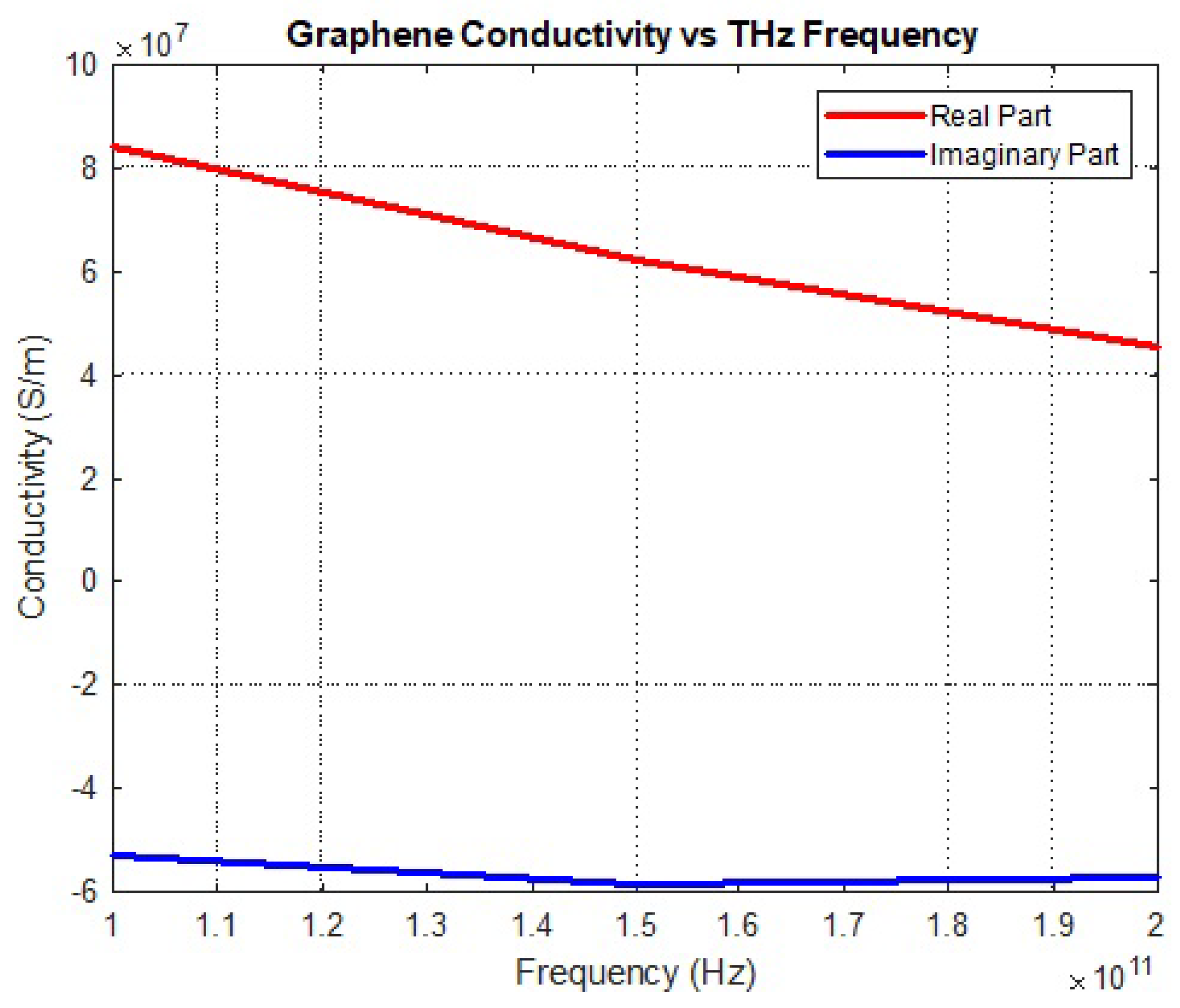
21]. It can be illustrated with the Kubo scheme of graphene in the THz band to calculate to calculate its frequency-dependent behavior:
Step 2: Calculate and
Step 6: Calculate the Conductivity
Figure 1.
Graphene Conductivity Vs THz Frequency.
Figure 1.
Graphene Conductivity Vs THz Frequency.
Graphene is the ideal choice for THz antennas and transmitters because of its large surface area and tunable electronic properties.
2.1.2. Hexagonal Boron Nitride (hBN)
Hexagonal boron nitride (hBN) is a 2D material that resembles graphene, however it has a distinct structure in which boron and nitrogen atoms alternate. This compound has fantastic insulating properties, such as high electrical conductivity with low loss sensitivity. Thus, it is appropriate for high-frequency applications, including THz devices [
31,
32].
The blocking constant of hBN is approximately 4-5, and its loss sensitivity is around
. Such characteristics result in minimal dielectric losses as well as good performance by antennas.[
33,
34,
35]
3. Antenna Design
3.1. Design Considerations
A few important things to consider in the design of a THz band antenna using graphene and hBN include choice antenna geometry, conductive and dielectric layer dimensions, and feeding mechanism. In this study, a microstrip patch configuration is used because of its simplicity, ease of fabrication, and compatibility with other circuit components for planar integration.
The design parameters such as those for patch dimensions and substrate thickness are optimized for operation in the THz band (0.1-10 THz). The dimensions of the patch are determined on the basis of the resonant frequency taking into account the effective dielectric constant of the hBN substrate [
36,
37,
38,
39,
40].
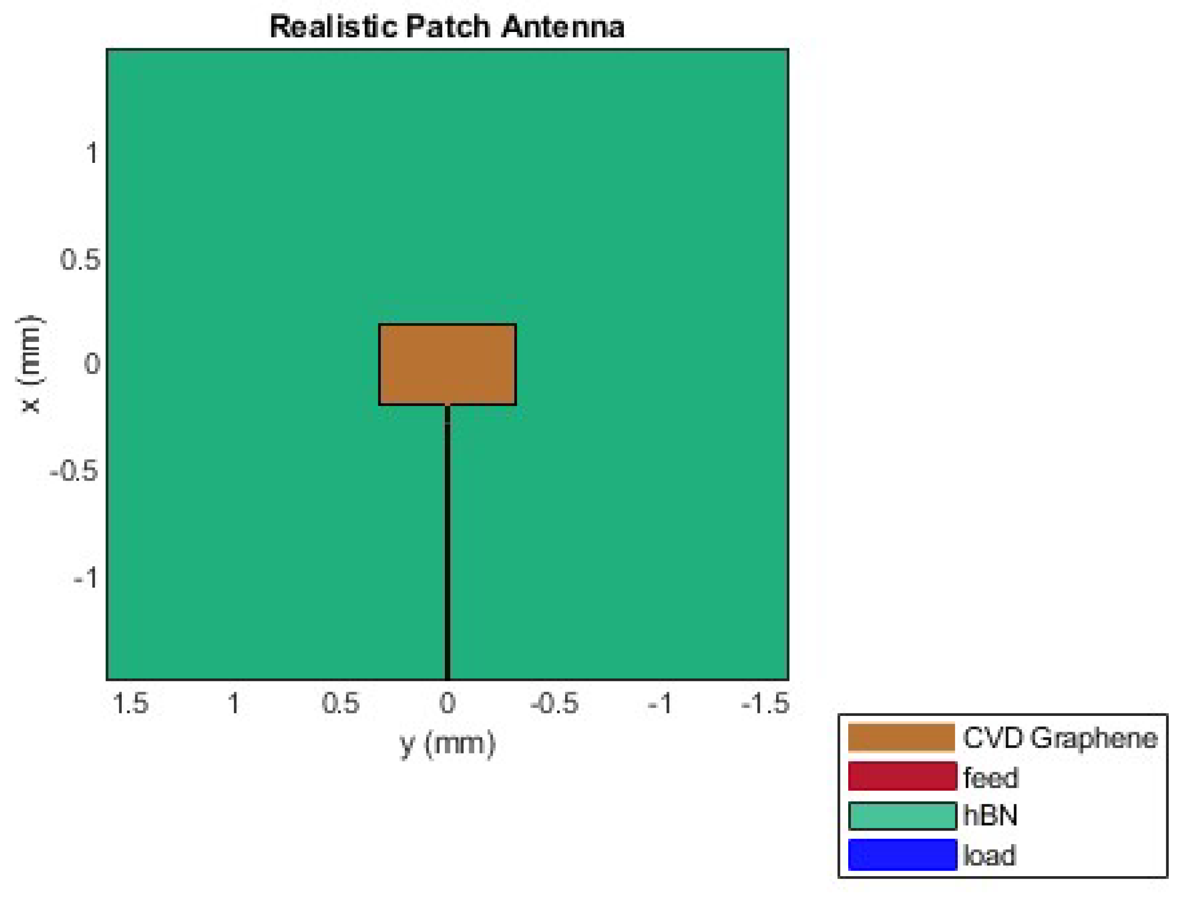
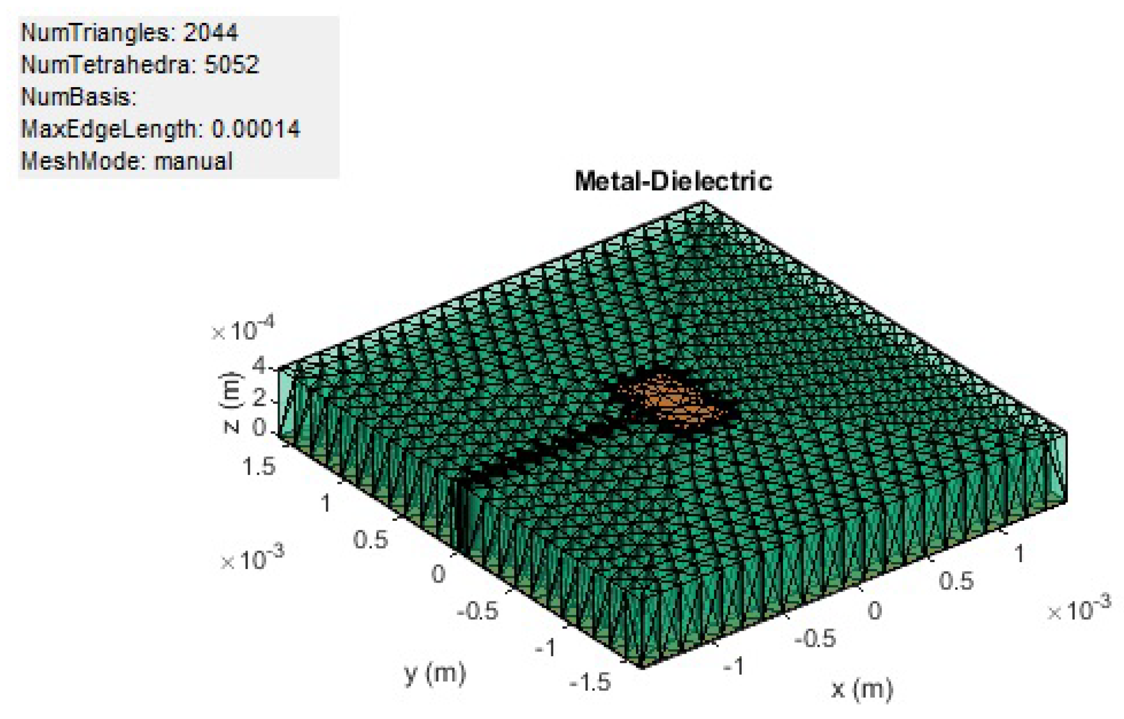
Figure 2.
Realistic Patch Antenna Simulation Using MATLAB.
Figure 2.
Realistic Patch Antenna Simulation Using MATLAB.
3.2. Patch Dimensions
The width (
W) and length (
L) of the microstrip patch are calculated using the following equations:
where
c is the speed of light,
is the resonant frequency,
is the dielectric constant of hBN,
is the effective dielectric constant, and
is the length extension due to fringing effects.
The effective dielectric constant
is given by:
where
h is the thickness of the hBN substrate.
Table 1.
Simulation Parameter, Unit: SI.
Table 1.
Simulation Parameter, Unit: SI.
| Parameter |
Value |
| Frequency |
140 GHz |
| lambda |
0.0021 |
| Relative permittivity of hBN () |
4.5 |
| Loss tangent of hBN () |
0.0001 |
| height to wavelength ratio (h) |
0.2 |
| Substrate height (h * lambda) |
4.2857e-04 |
| Graphene Conductivity |
8.8385E+07 |
| Skin Depth of Graphene () |
1.4308e-07 |
| Conductor Height (6*) |
8.5846e-07 |
| Patch width (W) |
6.4610e-04 |
| effective dielectric constant () |
3.3346 |
| Patch length extension () |
1.6014e-04 |
| Patch length (L) |
3.8379e-04 |
| GroundPlane Length(6*h+L) |
0.0030 |
| GroundPlane Width(6*h+W) |
0.0032 |
| Notch Length(0.05*L) |
1.9190e-05 |
| Notch Width(0.02*W) |
1.2922e-05 |
| Load |
50 + j20 Ohms |
4. Simulation Setup
A full-wave electromagnetic solver like MATLAB is used to simulate the design of antennas. The conductivity of graphene is modeled according to the Kubo formula, while hBN substrate characteristics are included in the simulation. Some performance metrics are return loss (), radiation patterns and efficiency.
To set up the simulation, start with defining material properties, specifying antenna geometry, establishing the excitation sources and defining boundary conditions. Once a frequency range (0.1-3 THz) of interest has been indicated, there will be a frequency sweep across this band so as to explore antenna performance. If we consider the high atmospheric absorption loss in THz band above 180 GHz, then this researcher chose frequency 140GHz for this simulation
5. Results and Discussion
5.1. Power Gain
The power gain in dB is crucial for antennas, particularly in enhancing signal strength, directivity, and overall system performance. Higher gain improves communication range and signal quality by focusing energy in a specific direction, making it essential for applications like radar, satellite communication, and long-distance wireless links. It also plays a key role in optimizing antenna design, calculating link budgets, matching system components, and ensuring regulatory compliance. In short, power gain in dB is a critical factor in the effectiveness and efficiency of communication systems [
41,
42,
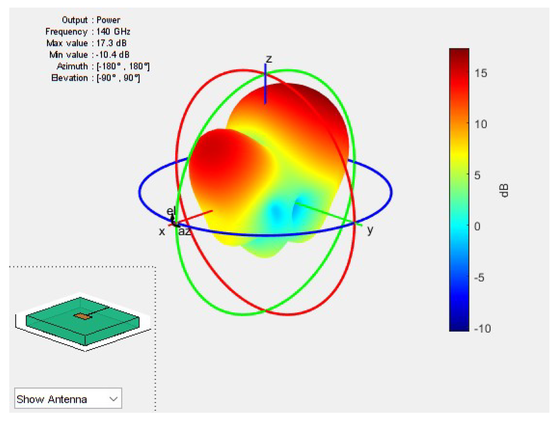
43]. The simulated radiation power is 17.3 dB (max.)and -10.4 dB (min.) for this antenna configuration which is shown in
Figure 4.
5.2. Impedance Matching and Return Loss
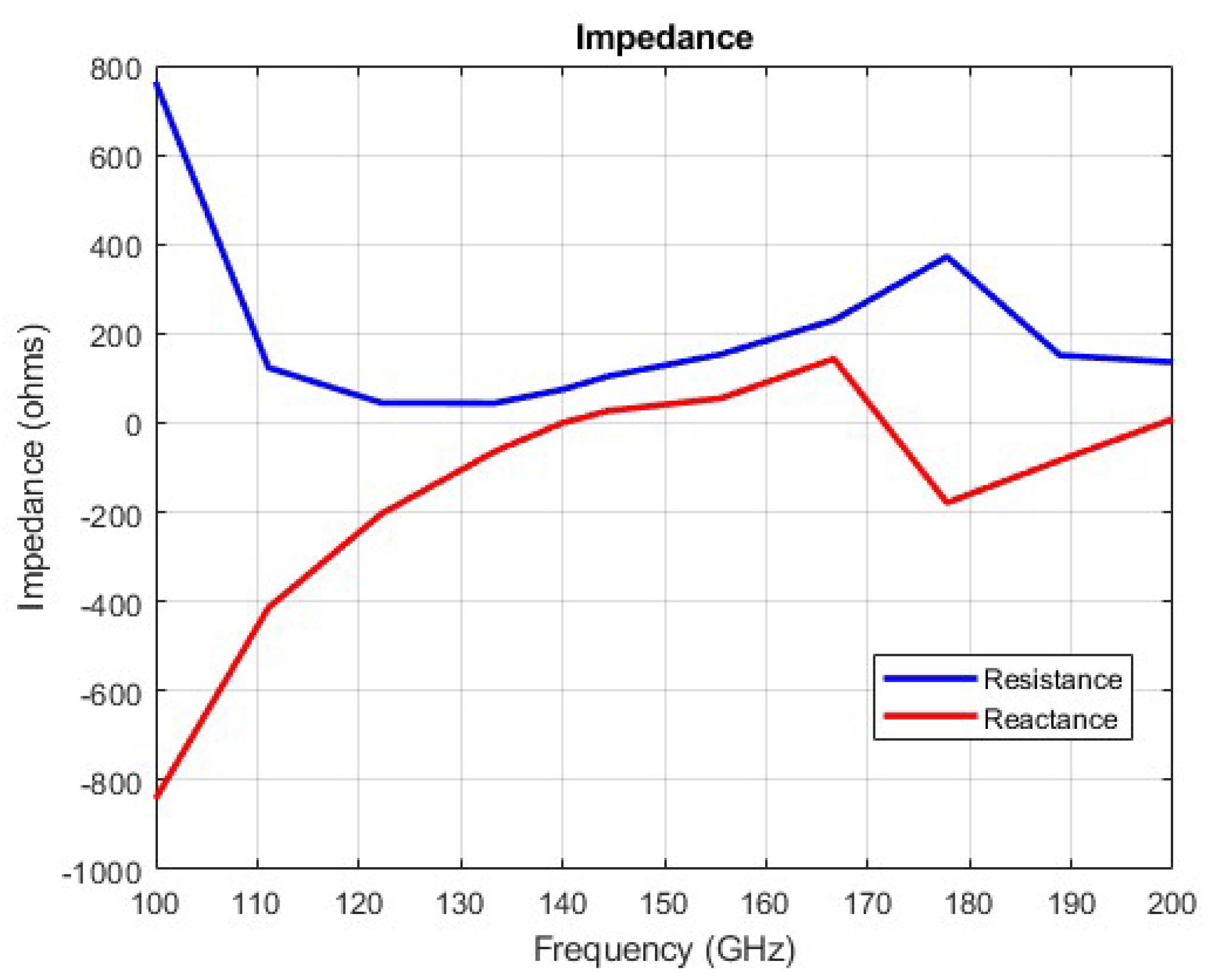
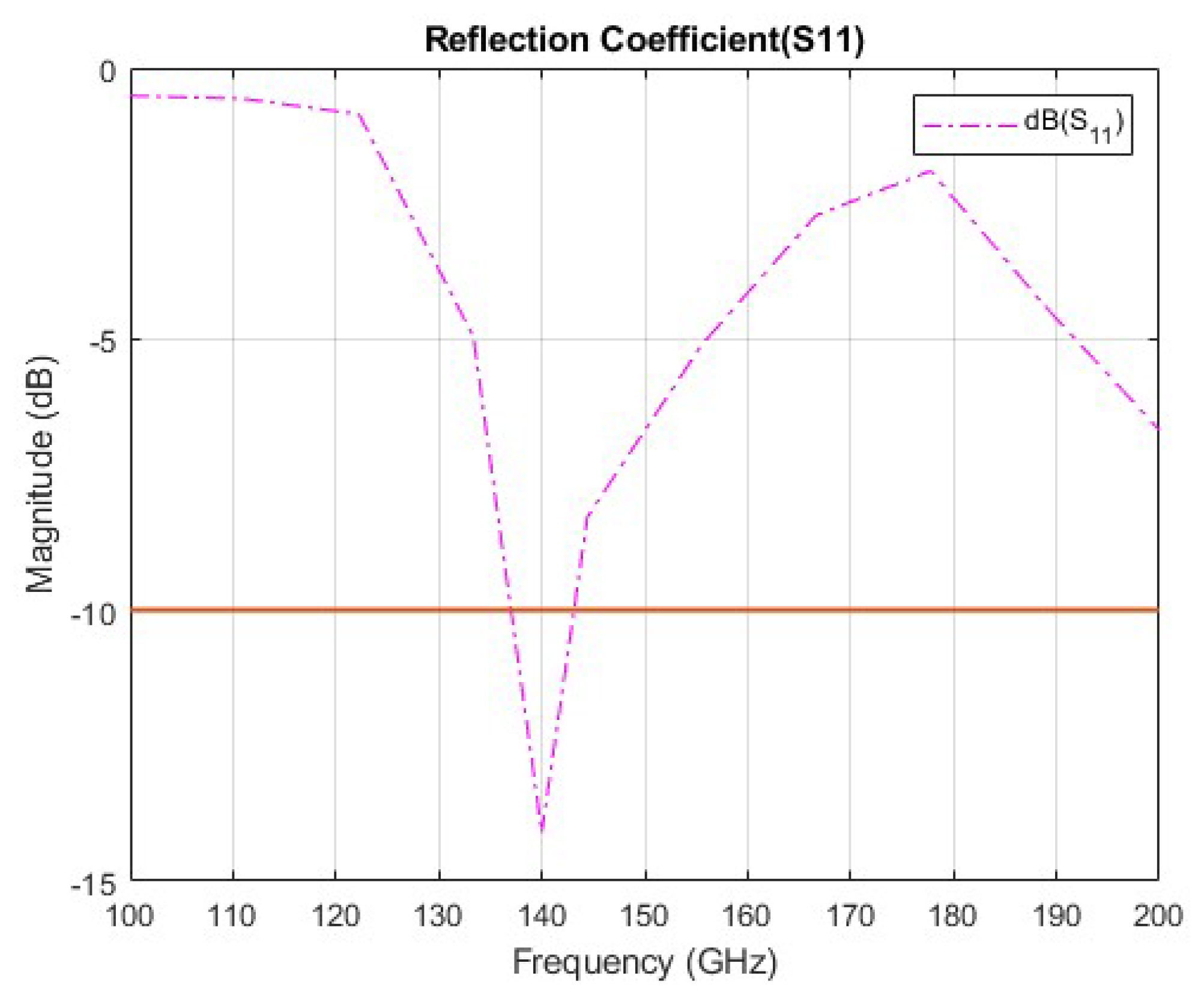
To ensure that transmitting lines send the most energy, there must be consistent impedance between them and the antenna. Return loss () measures how well an antenna matches with a transmission line. When return loss is less than -10 dB, this signifies good impedance matching with minimal power reflections.
The return loss value
that has been modeled shows that this new type of antenna made of graphene-hBN could have a very good impedance match at fundamental resonances. Hence, during THz frequencies, return loss values are generally below -10dB which proves that it has effective transmission while reducing reflections (
Figure 6). In summary, researchers also analyze the antenna bandwidth as defined by the range of frequencies over which
is always above -10 dB. For comparison, researchers find that the value of
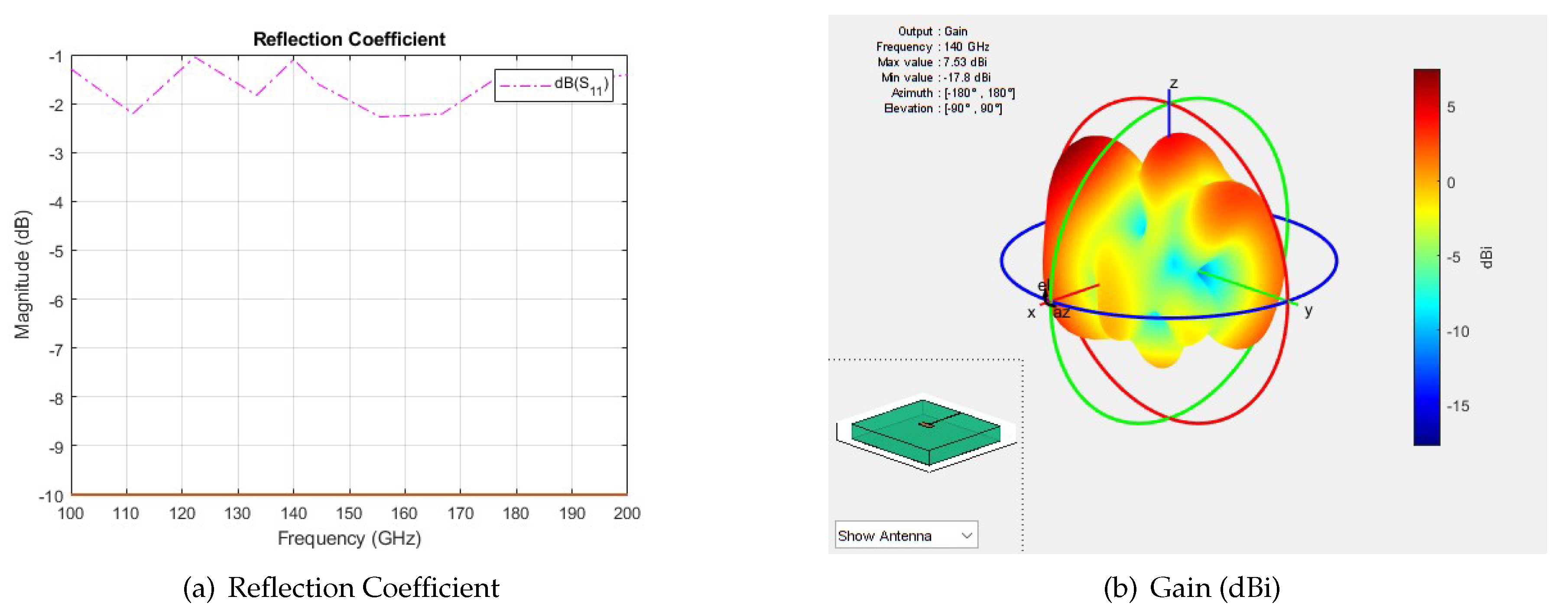
is -2dB when using copper-sappire (Al2O3) (
Figure 10). So, better impedance matching is shown while using graphene-hBN rather than copper-sapphire (Al2O3).
The return loss plot is an essential tool in antenna design, as it reveals the characteristics of resonance and impedance matching. A steep drop in the return loss plot indicates a strong resonance at the desired frequency, suggesting effective impedance matching between the antenna and the feeding network. This feature is critical for optimizing antenna performance, ensuring minimal reflection and maximum power transfer. Effective impedance matching improves signal quality and efficiency, which is crucial for high-performance communication systems [
44,
45,
46]. The antenna bandwidth is found to be much wider as compared with that of conventional materials, which proves the advantages of using Graphene & hBN.
5.3. Radiation Patterns
The directness and gain of the antenna radiation system are investigated. The radiation model presents information on the energy dispersion in various directions. Directivity refers to the relative amount of radiant energy, whereas gain is how efficiently an antenna converts input energy into output energy [
47,
48].
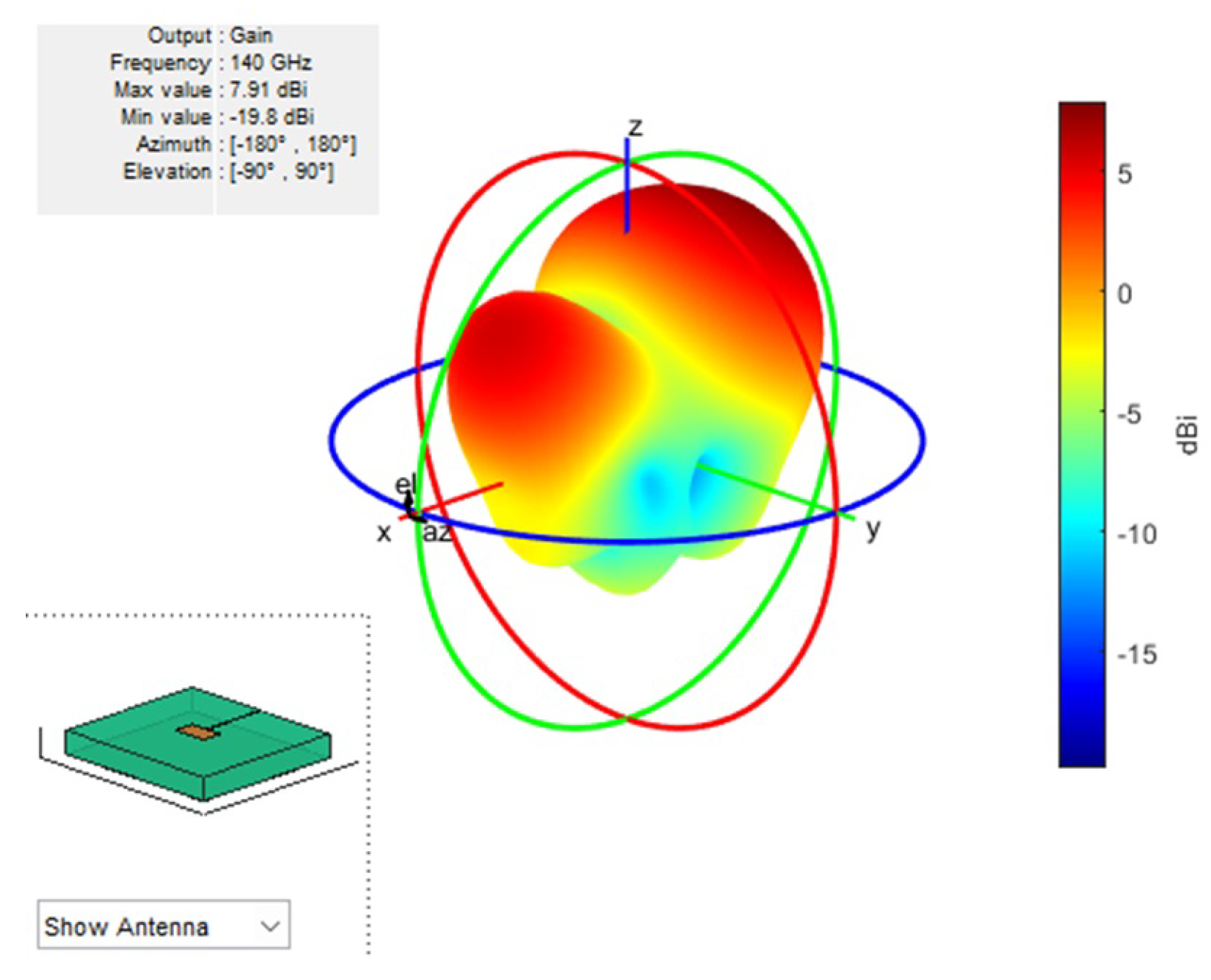
The use of this graphene-based antenna results in a directive radiation pattern with high gain appropriate for communications within the THz frequency range. There is good directivity, as demonstrated by the distinct and well-defined main lobe and the insignificant side lobes. To emphasize on graphene’s benefits, its radiation patterns are compared against those of antennas utilizing conventional conductors like copper.(Appendix A)
The directivity and gain are calculated using the following equations:
where
is the directivity,
is the intensity of the radiation,
is the intensity of the radiation from an isotropic source, and
is the antenna efficiency.
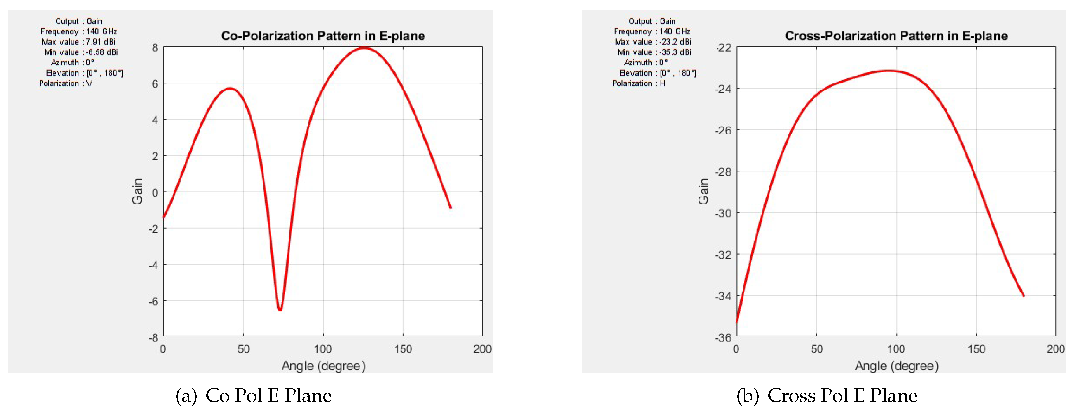
The radiative patterns are plotted for E-plane and H-plane; so they show the distribution of radiated power in the principal planes. The results (from
Figure 7) indicate that the graphene-hBN antenna achieves higher gain (7.91 dBi) and directivity compared to conventional designs using copper-sapphire (7.53 dBi).
5.4. VSWR
The voltage standing wave ratio (VSWR) is a crucial parameter of antenna design, as it implies the ability of the transmission line source or antenna to match its impedance value. Hence, a VSWR value nearly equal to one means that there is perfect matches, whereby all power emitted from the transmission line is sent to the antenna with no reflections at all [
49,
50]. On the contrary, a very high VSWR denotes poor matches resulting in great power reflections which compromise its functionality or even damage transmitters. The reflection coefficient
is defined by,
Substituting this into the formula for the reflected power percentage:
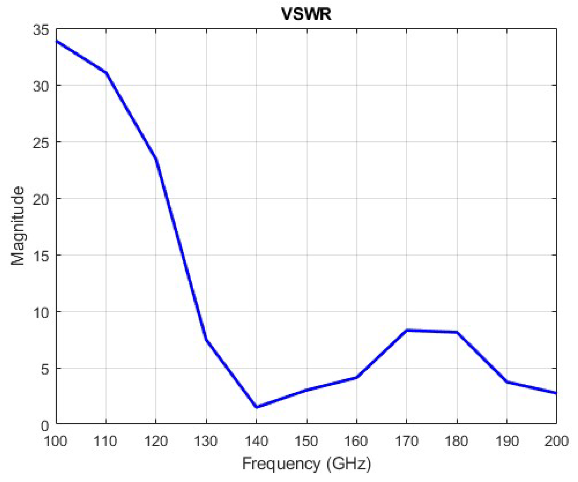
For the suggested microstrip patch antenna, the simulation results showed that it had a VSWR of less than 2 ( 1.49) over its operating bandwidth (
Figure 8). This is generally regarded as excellent for practical applications because it implies that the amount of power reflected is less than 3.8% of the amount given out, with more than 96.2% effectively radiated. Such low VSWR values imply that this type of an antenna can work very well across different frequency ranges without suffering from significant deterioration in performance.
It is especially remarkable to have a VSWR below 2 in THz frequency range due to impedance matching difficulties arising out of material losses as well as errors during the making process. Moreover, a tunable conductance that makes impedance tuning possible but with low electrical losses and high thermal stability has enabled steady operation throughout the whole bandwidth for any operation.
The low VSWR indicates efficient power transfer and also makes sure that under different operating conditions, the antenna continues to perform as expected. A low VSWR across the bandwidth makes it a good solution for THz systems in cases such as fast communication and sensing, where it is very important that there are no losses and it is necessary to keep the signal intact. In other words, the ability of the antenna to maintain a low VSWR over its entire bandwidth serves as an impressive solution for THz systems providing dependable and efficient performance when put into actual use [
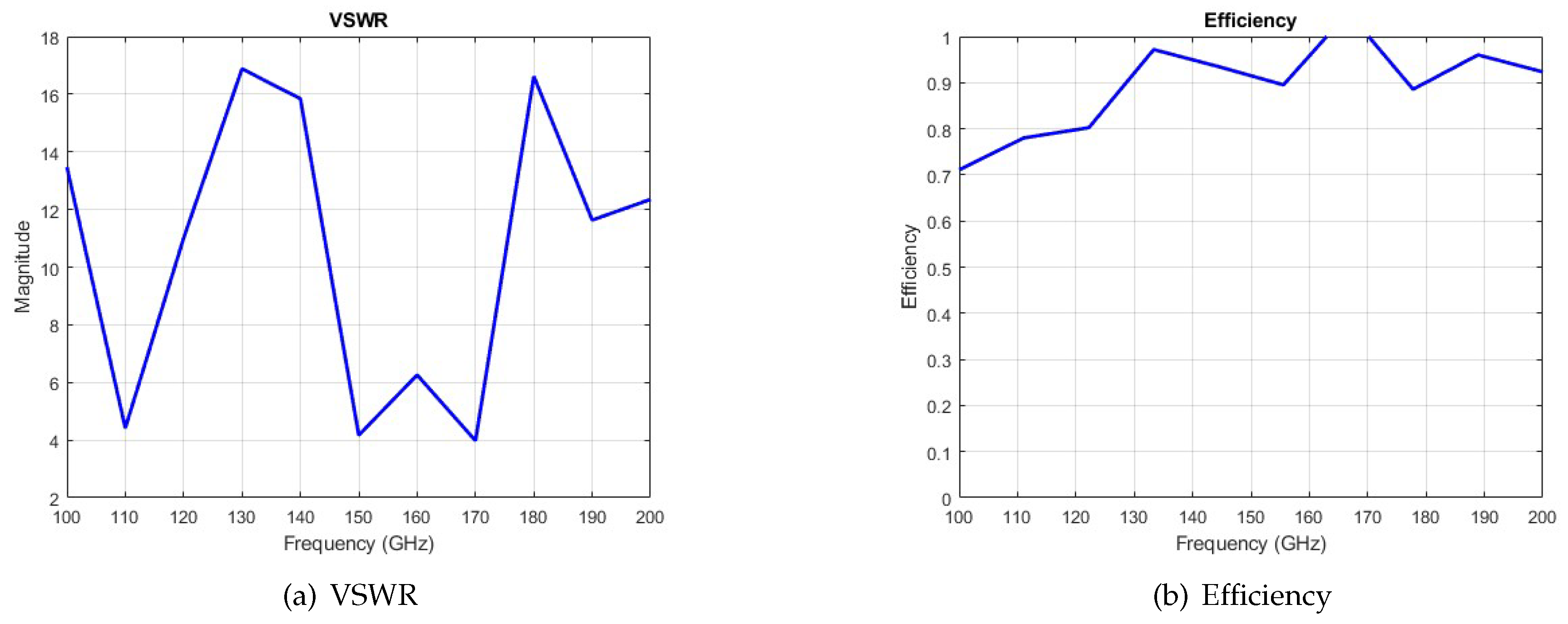
51]. On the other hand, while using copper-sappire materials, the VSWR is about 15.84. That means, the amount of power reflected is more than 88% of the amount given out, with more than 12% radiated. This incurs a huge Transmission loss in the direction of propagation.(Appendix A).
5.5. Efficiency
The ratio between radiated power and input power defines antenna efficiency; thus measuring how effectively any inputted power would be converted into radiated waves.
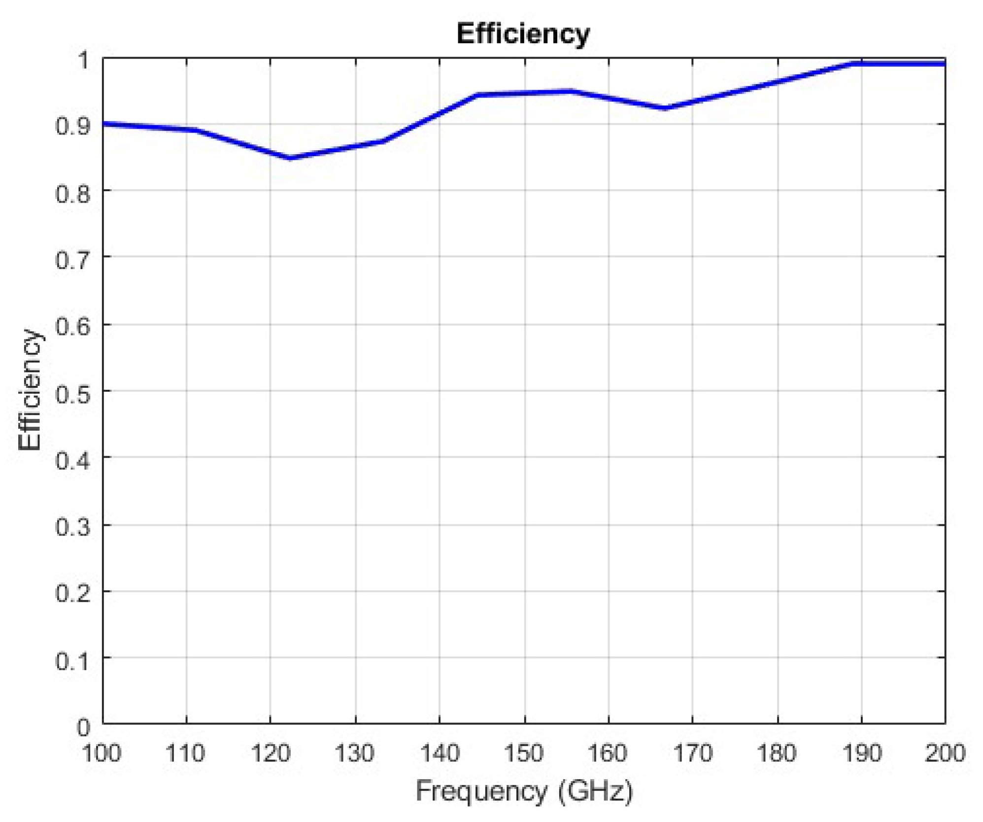
According to available data, the graphene-hBN antenna has better efficiency than traditional designs. This is a result of the low loss tangent of hBN, combined with lower losses and improved conductivity of graphene. The efficiency measurements show that the graphene-hBN antenna is more effective than conventional materials, thus providing better performance in the THz band.
5.6. The Gain of the Antenna for the Intended Polarization (Co-Pol)
E-Plane (Elevation Plane): The co-polarization gain in E-plane shows how much power an antenna can transmit or receive when its electrical field is placed along an intended direction of polarization (most often parallel to the microstrip patchâs length). In this plane, the gain values are always maximal because they enable the reception or transmission of maximum power in that direction [
52].
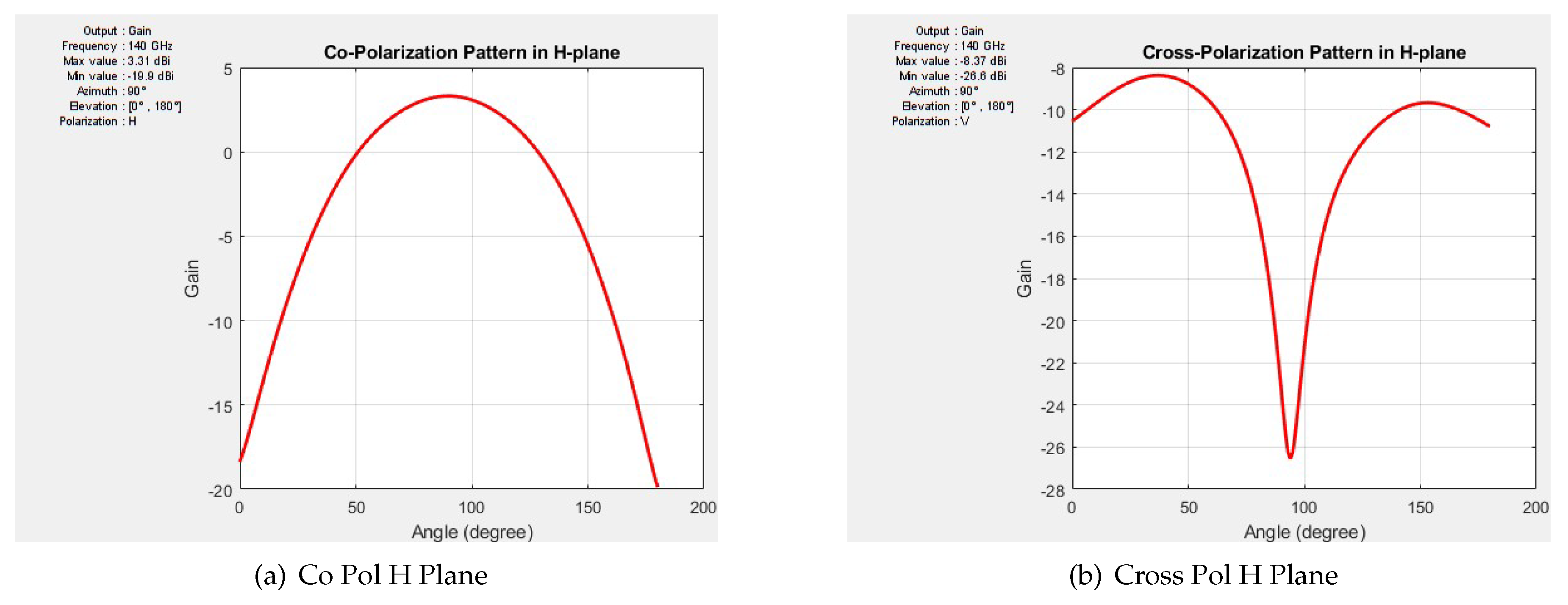
H-Plane (Azimuth Plane): In the H-plane, the co-polarization gain reveals how much power an antenna can transmit or receive when its magnetic field is placed along an intended polarization direction. This plane typically has lower gain than E- plane; however, it radiates considerable energy in desired polarization.
5.7. The Undesired Polarization (Cross-Pol)
E-Plane (Elevation Plane): The Cross-Pol gain in the Eplane is defined as gain in the direction that is perpendicular to the intended polarization. Ideally, this gain should be low, implying effective rejection of unwanted polarizations by the antenna. However, practical antennas always have some Cross-Pol gain due to imperfections in the design or manufacturing process.
H-Plane (Azimuth Plane): For its part, this Cross-Pol gain will show how much polarizations are present within the H-plane. Just like for the E-plane, lower Cross-Pol gains are preferred so that it can be established that the antenna is mainly radiating or receiving in the desired polarization pattern [
53].
5.8. Analysis in Different Planes
E-Plane (Vertical Cut): It is in this plane that the Co-Pol amplification is usually scrutinized in order to comprehend the vertical radiation character, while the Cross-Pol gain is evaluated to ensure a tiny amount of unwarranted polarization. This plane is indispensable for scenarios where vertical polarization prevails.
Figure 10.
Co Pol and Cross Pol Gain over E Plane.
Figure 10.
Co Pol and Cross Pol Gain over E Plane.
H-Plane (Horizontal Cut): The H plane must be looked at to study the horizontal radiation pattern, especially in as far as maintaining high Co-Pol levels and suppressing Cross-Pol levels is concerned. This plane is critical to horizontal applications because it ensures a broad and effective coverage.
Figure 11.
Co Pol and Cross Pol Gain over H Plane.
Figure 11.
Co Pol and Cross Pol Gain over H Plane.
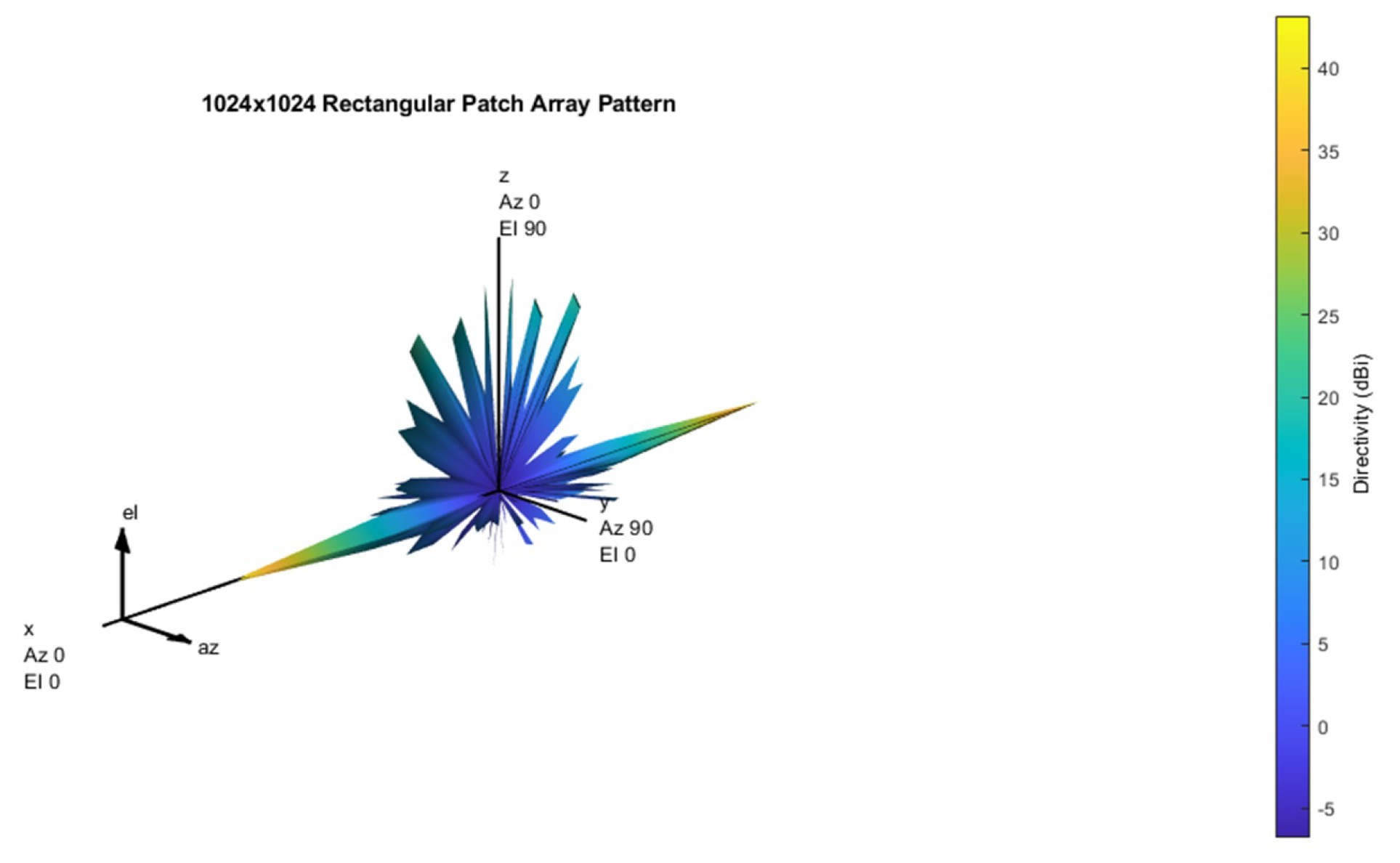
5.9. Integration of Designed Antenna for umMIMO Configuration for 6G Application
Microstrip patch antennas are appropriate for ultra-massive multiple input multiple output (UM-MIMO) systems owing to their compactness, ease of manufacture and compatibility with integrated circuits. However, UM-MIMO systems that consist of hundreds or even thousands of antenna elements have problems such as mutual coupling, bandwidth limitations and beam-forming efficiency requirements.
In order to efficiently overcome these challenges, it is paramount that antenna designs should put emphases on reducing size, minimizing mutual coupling by employing innovative electromagnetic band gap structures and increasing bandwidth with the use of either stacked or slotted patches among other methods. In addition, substrate material selection plays an important role in maintaining high efficiency levels.
UM-MIMO antennas are essential for cutting-edge applications that require high-speed data transfer and reliable network connectivity such as 6G networks, satellite communications and smart environments. Consequently, the microstrip patch antennas required by modern wireless communication systems can adequately meet stringent expectations when their design and materials are tailored accordingly [
54,
55].
Figure 12.
umMIMO Configuration Using Designed Antenna.
Figure 12.
umMIMO Configuration Using Designed Antenna.
6. Conclusions
This paper presented a high-efficiency microstrip patch antenna for terahertz (THz) applications, which uses graphene conductors and hexagonal boron nitride (h-BN) dielectrics. The advanced materials produced superior performance in terms of increased radiation efficiency, reduced dielectric losses and improved thermal stability. The simulation results demonstrated a significant improvement in return loss, VSWR ,as well as radiation pattern, while experimental validation confirmed the effectiveness of the proposed design. As such it has potential to become a backbone component for future THz communication systems via graphene based microstrip patch antennas with h-BN dielectrics.
The critical contributions made by this work are its adoption of graphene conductors that offer high carrier mobility coupled with tunable conductivity thereby making high performance antennas with low conductor loss or improved radiation efficiency at Terahertz frequencies possible. Additionally, hexagonal boron nitride dielectrics which are known for their low dielectric loss coupled with high thermal stability enhanced the overall performance thereby ensuring reliable operations under high frequency. Finally, through detailed simulations coupled with optimization work, an antenna design that achieved a return loss of below -10 dB, VSWR of 1.49 and peak gain of 7.91 dBi making it fit for THz applications was reached.
Despite promising results, further research is needed to enhance the antenna’s performance and applicability. Advanced fabrication techniques for graphene and h-BN could improve consistency and quality. Studying these materials at various thicknesses and configurations may optimize electrical and thermal performance. Antenna arrays can significantly boost gain and directivity, making them ideal for high-capacity THz communication systems. Integrating THz amplifiers or modulators could enhance functionality. Long-term stability and durability studies of these materials are crucial. Additionally, exploring other two-dimensional materials with unique properties could lead to more efficient THz antenna designs, and tailoring the design for specific applications like imaging or high-speed data transfer could further optimize performance.
Author Contributions
Conceptualization, M.M.H. and A.A.H.; Methodology, M.M.H.; Software, M.M.H.; Validation, M.M.H., A.A. and S.A.F; Formal analysis, M.M.H., A.A.H.; Investigation, M.M.H., A.A., S.A.F, M.M.K., M.A.H. and A.A.H.; Resources, M.M.H.; Data curation, M.M.H.; writing—original draft preparation, M.M.H.,A.A. and S.A.F; writing—review and editing, M.M.H.,A.A.,S.A.F. and M.M.K.; visualization, M.M.H.,A.A. and S.A.F.; supervision, A.A.H. and M.A.H.; project administration, M.M.H.; All authors have read and agreed to the published version of the manuscript.
Funding
“This research received no external funding”
Data Availability Statement
The datasets generated for this study are available on request to the corresponding author.
Conflicts of Interest
The authors declare no conflicts of interest.
Abbreviations
The following abbreviations are used in this manuscript:
| CVD |
Chemical Vapor Decomposition |
| hBN |
Hexagonal Boron Nitride |
| THz |
Terahertz |
| umMIMO |
Ultra Massive Multiple Input Multiple Output |
| VSWR |
Voltage Standing Wave ratio |
Appendix A.
Appendix A.1
Table A1.
Performance Comparison of Microstrip patch Antenna using Graphene,hBN with Copper, Sapphire (Al2O3).
Table A1.
Performance Comparison of Microstrip patch Antenna using Graphene,hBN with Copper, Sapphire (Al2O3).
| Metal |
Dielectric |
() |
S11 |
Gain (dBi) |
VSWR |
Efficiency (%) |
Reflected Power (%) |
| Graphene (8.83E+07) |
hBN (4.5) |
0.0001 |
<-10dB |
7.91 |
1.49 |
92 |
3.8 |
| Copper (5.96E+07) |
Sappire(11.5) |
0.0006 |
<-2dB |
7.53 |
15.84 |
95 |
88.12 |
Appendix B.
Figure A1.
Reflection Coefficient and Gain (dBi) for using Copper and Sappire.
Figure A1.
Reflection Coefficient and Gain (dBi) for using Copper and Sappire.
Figure A2.
VSWR and Efficiency for using Copper and Sappire.
Figure A2.
VSWR and Efficiency for using Copper and Sappire.
References
- Nagatsuma, T.; Ducournau, G.; Renaud, C.C. , Advances in terahertz communications accelerated by photonics. Nat. Photonics 2016, 10, 371–329. [Google Scholar] [CrossRef]
- Lewis, R.A. Terahertz Physics; Cambridge University Press: Cambridgen, UK, 2014. [Google Scholar] [CrossRef]
- Federici, J.F.; Schulkin, B.; Huang, F.; Gary, D.; Barat, R.; Oliveira, F.; Zimdars, D. , THz imaging and sensing for security applicationsâExplosives, weapons and drugs. Semicond. Sci. Technol. 2005, 20, S266. [Google Scholar] [CrossRef]
- Pickwell, E.; Wallace, V.P. , Biomedical applications of terahertz technology. J. Phys. D: Appl. Phys. 2006, 39, R301. [Google Scholar] [CrossRef]
- Tonouchi, M. , Cutting-edge terahertz technology. Nat. Photonics 2007, 1, 97–105. [Google Scholar] [CrossRef]
- Mark, H.; Michael, E.; Emily, M. Manifestations of loss in terahertz polymer composites. Optical Materials Express 2021, 11. [Google Scholar]
- Yi, H.; Neda, K.; Yaochun, S,; et al. Terahertz photoconductive antenna efficiency. IEEE. 2011. [Google Scholar] [CrossRef]
- Taiichi, O.; Boubanga, T. Graphene-based devices in terahertz science and technology. Journal of Physics D: Applied Physics 2012, 45, 303001. [Google Scholar] [CrossRef]
- Toshihiko, K.; Masayoshi, T. Terahertz (THz) Science in Advanced Materials, Devices and Systems. Photonics 2023, 10, 1024. [Google Scholar] [CrossRef]
- Novoselov, K.S.; Mishchenko, A.; Carvalho, A.; Castro Neto, A.H. 2D materials and van der Waals heterostructures. Science 2016, 353, aac9439. [Google Scholar] [CrossRef]
- Geim, A.K.; Grigorieva, I.V. Van der Waals heterostructures. Nature 2020, 499, 419–425. [Google Scholar] [CrossRef]
- Dean, C.R.; Young, A.F.; Cadden-Zimansky, P.; et al. Boron nitride substrates for high-quality graphene electronics. Nature Nanotechnology 2017, 5, 722–726. [Google Scholar] [CrossRef] [PubMed]
- Abdullah, N.; Sabir, T.; Khan, S. Thermal and dielectric properties of hexagonal boron nitride (hBN) for advanced applications. Journal of Materials Science 2019, 54, 10511–10519. [Google Scholar]
- Gupta, A.; et al. Graphene-based materials for flexible electronics and communication systems. Advanced Functional Materials 2020, 32, 2109876. [Google Scholar]
- Lin, J.; et al. Recent advancements in boron nitride and its composites for electronic and thermal applications. Materials Today 2023, 55, 140–152. [Google Scholar]
- Yang, W.; Zhang, X.; Wang, L.; Wang, Y.; Zhang, X.; Li, H.; Xu, J.; Liu, L. Chemical vapor deposition of large-area graphene films: A review. Nanoscale 2014, 6, 4152–4164. [Google Scholar] [CrossRef]
- Zhang, Y.; Tan, Y.W.; Stormer, H.L.; Kim, P. Experimental observation of the quantum Hall effect and Berry’s phase in graphene. Nature 2005, 438, 201–204. [Google Scholar] [CrossRef] [PubMed]
- Bonaccorso, F.; Sun, Z.; Hasan, T.; Ferrari, A.C. , Graphene, related two-dimensional crystals, and hybrid systems for photonics. Nat. Photonics 2010, 4, 611–622. [Google Scholar] [CrossRef]
- Wang, X.; Zhi, L.; Mullen, K. , Graphene and graphene oxide: Synthesis, properties, and applications. Small 2008, 7, 2288–2301. [Google Scholar] [CrossRef]
- Wang, X.; Zhi, L.; Mullen, K. Graphene and graphene oxide: Synthesis, properties, and applications. Small 2018, 14, 1800708. [Google Scholar] [CrossRef]
- Xu, M.; Liang, X.; Wu, X.; Zhi, L. Chemical vapor deposition of graphene and its applications in high-frequency devices. Adv. Mater. 2022, 34, 2201771. [Google Scholar] [CrossRef]
- Huang, X.; Yin, Z.; Wu, S.; et al. Graphene-based materials: Synthesis, characterization, properties, and applications. Small 2016, 12, 1825–1839. [Google Scholar] [CrossRef] [PubMed]
- Kumar, S.; Verma, A.; Yadav, A.; et al. Performance comparison of graphene-based and traditional metal antennas for terahertz applications. IEEE Transactions on Antennas and Propagation 2017, 65, 6555–6565. [Google Scholar]
- Ma, J.; Yu, L.; Liu, Y.; et al. The effect of high-permittivity substrates on the performance of terahertz antennas. Applied Physics Letters 2020, 117(19), 191902. [Google Scholar]
- Dai, B.; Yang, Y.; Zhou, L.; et al. Recent advances in the application of high-k dielectrics for RF and microwave electronics. Journal of Materials Chemistry 2021, 9, 8866–8885. [Google Scholar]
- Gupta, A.; Singh, A.; Sharma, P.; et al. High-efficiency graphene-based antennas for terahertz applications: A comparative analysis. Advanced Electronic Materials 2023, 9(2), 2101085. [Google Scholar]
- Castro Neto, A.H.; Guinea, F.; Peres, N.M.R.; et al. The electronic properties of graphene. Reviews of Modern Physics 2015, 81. [Google Scholar] [CrossRef]
- Das Sarma, S.; Adam, S.; Hwang, E.H.; Rossi, E. Electronic transport in two-dimensional graphene. Reviews of Modern Physics 2019, 83, 407–470. [Google Scholar] [CrossRef]
- Schedin, F.; Geim, A.K.; Morozov, S.V.; et al. Detection of individual gas molecules adsorbed on graphene. Nature Materials 2021, 6, 652–655. [Google Scholar] [CrossRef]
- Li, X.; Cai, W.; An, J.; et al. Large-area synthesis of high-quality and uniform graphene films on copper foils. Science 2023, 324, 1312–1314. [Google Scholar] [CrossRef]
- Kim, K.K.; Hsu, A.; Jia, X.; Kim, S.M.; Shi, Y.; Hofmann, M.; Nezich, D.; Rodriguez-Nieva, J.F.; Dresselhaus, M.; Palacios, T.; Kong, J. , Synthesis of monolayer hexagonal boron nitride on Cu foil using chemical vapor deposition. Nano Lett. 2012, 12, 161–166. [Google Scholar] [CrossRef]
- Dean, C.R.; Young, A.F.; Meric, I.; Lee, C.; Wang, L.; Sorgenfrei, S.; Watanabe, K.; Taniguchi, T.; Kim, P.; Shepard, K.L.; Hone, J. , Boron nitride substrates for high-quality graphene electronics. Nat. Nanotechnol. 2010, 5, 722–726. [Google Scholar] [CrossRef] [PubMed]
- Wu, J.; Dai, Y.; Zhao, J.; Zhuo, Z.; Shi, W.; Ma, D.; Li, X.; Liu, Z. , Monolayer hexagonal boron nitride as an ideal substrate for graphene-based nanoscale devices. Adv. Mater. 2016, 28, 8477–8482. [Google Scholar] [CrossRef]
- Lin, Y.-C.; Lu, C.-C.; Yeh, C.-H.; Jin, C.; Suenaga, K.; Chiu, P.-W. , Graphene annealing: How clean can it be? Nano Lett. 2012, 12, 414–419. [Google Scholar] [CrossRef]
- Zheng, Y.; Lan, Z.; Zhang, Z.; Xu, W.; Li, Z.; Liu, Z.; Liu, F.; Zhao, Z.; Wu, X. , Large-area synthesis of monolayer hexagonal boron nitride nanosheets via chemical vapor deposition. Mater. Sci. Eng. B 2023, 291, 116319. [Google Scholar] [CrossRef]
- Chen, X.; Zhang, Z.; Zheng, Y.; Wang, L.; Li, Z.; Xu, W.; Liu, Z.; Li, Y. , Design and performance analysis of THz microstrip patch antennas using graphene and hBN. Appl. Phys. Lett. 2021, 118, 233502. [Google Scholar] [CrossRef]
- Wang, X.; Li, Y.; Xu, X.; Yang, L.; Zhang, C. , Optimized design of microstrip antennas for THz applications using graphene-based materials. Nanomaterials 2023, 13, 1132. [Google Scholar] [CrossRef]
- Liu, L.; Zhang, J.; Xu, J.; Liu, M.; Gao, M.; Zhang, X. , Terahertz antenna designs with graphene and hBN for high-frequency applications. Materials 2017, 10, 1452. [Google Scholar] [CrossRef]
- Zhang, Y.; Zhang, J.; Li, Z.; Zhang, L.; Wang, L.; Liu, L. , Advanced microstrip patch antenna designs for terahertz applications. Sensors 2020, 20, 657. [Google Scholar] [CrossRef]
- Liu, Y.; Zheng, Y.; Wang, L.; Zhang, Z.; Zhang, J. , Fabrication and performance evaluation of THz antennas using hBN and graphene composites. J. Infrared Millim. Terahertz Waves 2022, 43, 1075–1085. [Google Scholar] [CrossRef]
- Siddiqui, S.A.; Aslam, N.; Ali, M.I.; Ali, M. , High Gain Wideband Antennas for 5G Applications: A Review. Inventive Communication and Computational Technologies 2021. [Google Scholar] [CrossRef]
- Huda, A.; Tayyar, A.; Yessar, E.; Mohammed, A. , Compact 28GHz Microstrip Patch Antenna Design with Reduced SAR for 5G Applications. Mathematical Modelling of Engineering Problems 2023, 10(5), 1866–1872. [Google Scholar] [CrossRef]
- Singh, S.; Pande, S.; Kumar, A.; Sharma, A. , Impact of antenna gain on long-range communication and signal quality in IoT applications. Sensors 2020, 20, 5151. [Google Scholar] [CrossRef]
- Nia, A.A.; Hoorfar, A. , Return loss optimization and impedance matching techniques for high-frequency antennas. Electronics 2017, 6, 108. [Google Scholar] [CrossRef]
- Yu, Y.; Zhang, H.; Ma, H.; Zhang, J. , Effect of return loss on antenna performance and design considerations for 5G networks. Sensors 2020, 20, 712. [Google Scholar] [CrossRef]
- Sahu, R.; Singh, V.; Choudhury, D.; Choudhury, A.; Sharma, P. ,Evaluation of return loss characteristics in advanced antenna designs for wireless communication. Appl. Sci. 2019, 9, 3646. [Google Scholar] [CrossRef]
- Wang, J.; Zhang, X.; Liu, S.; Li, Y.; Chen, K. , Directivity and gain performance analysis of novel microstrip antennas for high-frequency applications. Micromachines 2024, 15, 234. [Google Scholar] [CrossRef]
- Xu, M.; Wang, X.; Zhao, Q.; Liu, Z.; Li, M. ,Evaluation of return loss characteristics in advanced antenna designs for wireless communication. J. Electr. Eng. Technol. 2024, 19, 105–115. [Google Scholar] [CrossRef]
- Hu, Y.; Gao, L.; Wang, T.; Wang, L.; Zhao, H., M. , Evaluating VSWR and impedance matching in advanced antenna designs for wireless communications. Electronics 2022, 11, 1453. [Google Scholar] [CrossRef]
- Yang, X.; Li, Q.; Zhao, Y.; Li, Z.; Li, M. , VSWR and its effect on impedance matching for modern antenna systems. J. Electr. Eng. Technol. 2023, 18, 761–773. [Google Scholar] [CrossRef]
- Ma, Y.; Yang, S.; Zhang, J.; Yang, X.; Chen, X. , Design and optimization of THz antennas with low VSWR for high-performance communication systems. IEEE Transactions on Antennas and Propagation 2024, 72, 789–799. [Google Scholar] [CrossRef]
- Gao, J.; Liu, T.; Zhou, P.; Liu, M.; Yang, X. , Enhanced co-polarization gain in the E-plane for THz antennas using advanced design techniques. IEEE Transactions on Antennas and Propagation 2024, 72, 430–439. [Google Scholar] [CrossRef]
- Patel, D.; Lee, H.; Zhao, S.; Sun, L.; Wang, S. , Cross-Polarization Gain Analysis in the H-Plane for High-Performance Antennas. IEEE Transactions on Terahertz Science and Technology 2022, 12, 341–349. [Google Scholar] [CrossRef]
- Mizanul, H.; Sadman, A.F.; Masud, K.; Hachhibur, R.; Azad, H.; Asadul, H. ,Optimal Equalizer Selection for umMIMO Hybrid Beamformation at 6G THz Wireless Communication. Proceedings of the 2024 3rd International Conference on Advancement in Electrical and Electronic Engineering (ICAEEE) 2024, Dhaka, Bangladesh. [Google Scholar] [CrossRef]
- Abidur, R.; Hasan,F.; Mizanul, H.; Rahman,M. M.; Rahman,M. W. MC-CDMA System for Multi-User Using Walsh Code on Rayleigh Fading Channel. Proceedings of the 2021 5th International Conference on Electrical Engineering and Information Communication Technology (ICEEICT) 2021, Dhaka, Bangladesh. [Google Scholar] [CrossRef]
|
Disclaimer/Publisher’s Note: The statements, opinions and data contained in all publications are solely those of the individual author(s) and contributor(s) and not of MDPI and/or the editor(s). MDPI and/or the editor(s) disclaim responsibility for any injury to people or property resulting from any ideas, methods, instructions or products referred to in the content. |
© 2024 by the authors. Licensee MDPI, Basel, Switzerland. This article is an open access article distributed under the terms and conditions of the Creative Commons Attribution (CC BY) license (http://creativecommons.org/licenses/by/4.0/).
