1. Introduction
Plasmonics and its applications is based on the optical processes that occur in metallic nanostructures involving the coupling of light and collective oscillations of conduction band electrons (known as plasmons) at the metal–dielectric interface. The size, shape, and composition of the nanostructures can be engineered to manipulate the properties of the plasmons, such as their resonance frequency and localization, which, in turn, can enable a wide range of applications in various fields [
1,
2,
3,
4,
5].
In addition, the application of plasmonics represents a good opportunity for nano-optomechanics to explore the interaction between light and mechanical motion at the nanoscale, enabling ultra-sensitive mass detection, precision measurement of forces, and advancements in quantum information processing [
6,
7,
8,
9]. These systems typically utilize nanoscale resonators where light controls and measures mechanical vibrations. Achieving strong optomechanical coupling relies on the ability to localize and enhance electromagnetic fields at the nanoscale. Metallic nanostructures possess the ability to confine light below the diffraction limit via the excitation of localized surface plasmons (LSPs), the oscillations of free electrons at the surface of metallic nanostructures, offering a powerful means of confining light to sub-wavelength dimensions [
10,
11]. LSPs can interact with mechanical vibrations, making them ideal for studying nanoscale mechanical oscillations and enhancing optomechanical interactions [
12,
13,
14]. Investigating systems with high LSP confinement is crucial for advancing nano-optomechanical applications.
Among the nanostructures supporting highly confined LSPs, one can cite nanoparticles-on-mirror (NPsOM) (or film-coupled nanoparticles) [
15,
16], where a metal nanoparticle is separated from a metal film by a thin dielectric layer acting as a spacer; these structures have attracted significant attention due to their ease of fabrication [
17] and the ability to trap plasmon modes in ultrasmall volumes [
18,
19,
20]. The response of NPsOM can be significantly influenced by the thickness of the metal film [
21,
22], as thinner metal films tend to result in stronger coupling between the nanoparticle and the film, leading to more pronounced plasmonic effects, while thicker films may reduce this interaction and broaden the resonance linewidths. Similarly, the interspacing between the gold film and the nanoparticle [
23] and the shape of the nanoparticles plays a crucial role in determining the plasmonic properties [
24]. Also, NPsOM with dimers or trimers atop the metal film, as opposed to monomers, are expected to exhibit more interesting and/or improved features such as narrower plasmon linewidths and more pronounced scattered intensity [
13,
25].
This study focuses on investigating numerically based on the finite element method (FEM), LSPs in a structure design in the category of NPsOM devices, consisting of nano-ridges deposited on a gold layer, with a polymer layer acting as a spacer. It is worth mentioning that such a design could be readily fabricated experimentally given the state-of-the-art technology [
26]. We first investigate the LSPs modes of a single ridge by examining its scattering cross section in the visible and near-infrared range. To introduce additional LSPs modes, we insert a thin polymer layer at the middle of the ridge, which results in new LSPs confined within such a layer. Then, we explore the dimer configuration, which has been proven to show more interesting characteristics [
13,
25]. Our findings indicate that dimerization, achieved by positioning two ridges in close proximity, enhances the interaction between the modes, leading to LSPs resonances with significantly improved quality factors—approximately a threefold enhancement compared to a single monomer. Additionally, the polymer layer at the middle of the ridges plays an important role in enhancing the localization of the plasmon field and the quality factor of the different modes as compared to previous reports [
13]. In a recent paper [
27], we have studied localized phonons in a similar monomer and dimer structures. Here, we show prospectively based on the dimer LSPs modes effective volumes, how such modes would couple with the localized phonons in the dimer, thereby enabling their classification in terms of optomechanical coupling intensity.
This paper is organized as follows: In Section II, we present a detailed investigation of the LSPs of a single gold nano-ridge positioned atop a multilayer structure. In Sec. III, we extend this analysis to a coupled gold nanoridges, examining how the dimer configuration influences the localization and enhancement of the plasmonic modes. In Sec. IV, we provide an analysis of the mode volume for each LSP mode, enabling the classification of the different LSP modes and discussing their potential applications in acousto-plasmonic interactions.
2. Localized Surface Plasmons of a Single Gold Nano-Ridge
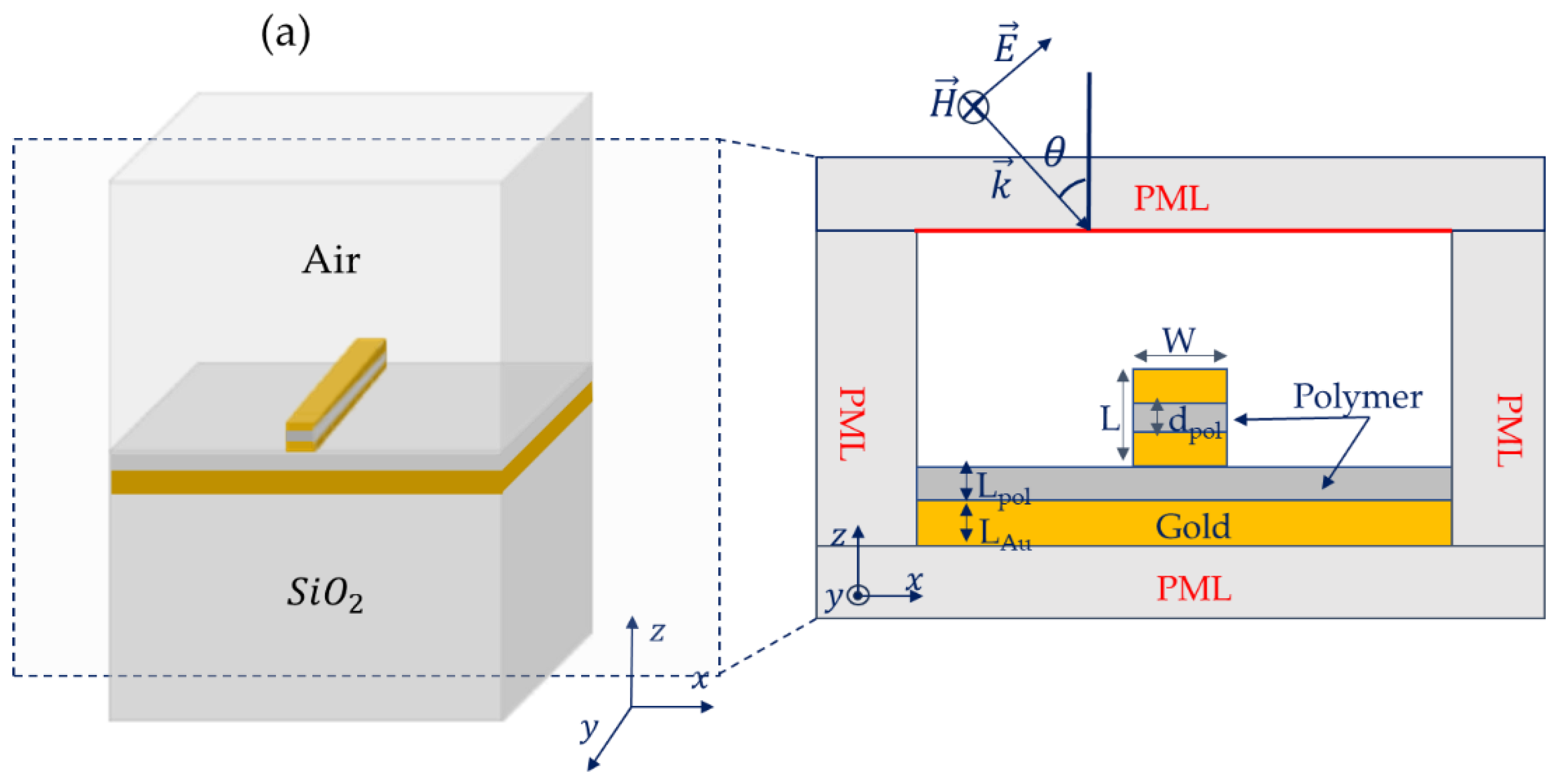
The proposed design is shown in
Figure 1a. It consists of a gold nano-ridge with a thin polymer layer lying in the middle, deposited above a polymer thin spacer layer made of the same material, that covers a gold thick film beneath. Experimentally speaking, the whole design could be grown on a silicon dioxide substrate (SiO
2), but in terms of simulations the thick gold film absorbs and reflects all incident light before reaching SiO
2. Hence, the latter medium is excluded from simulations. Due to the system’s symmetry along the y-axis, all calculations were performed in the x-z plane.
The modeled cross-section of the system is depicted in
Figure 1a. The parameters of the studied system are as follows: W is the nano-ridge width while L is its height, d
pol is the thickness of the polymer layer inserted in the middle of the ridge, L
pol is the thickness of the polymer spacer layer and L
Au is the thickness of the gold layer beneath. The simulation results presented in this work were obtained using electromagnetic frequency domain analysis based on the FEM, using COMSOL Multiphysics software. In order to excite the system, a plane light-wave with TM polarization is launched from the incidence medium at the top, at oblique incidence onto the latter, as shown in
Figure 1a. To eliminate undesirable reflections at the edges of the system, perfectly matched layers (PMLs) were placed on all boundaries. The materials used include a polymer with the refractive index,
, while for dispersive materials namely, the gold metal, a frequency-dependent complex-valued relative permittivity based on the Lorentz-Drude model was adopted [
28]:
where the sum over m corresponds to different oscillators,
is the high-frequency contribution to the relative permittivity,
is the plasma frequency of free electrons,
is the oscillator strength,
is the resonance frequency, and
is the damping coefficient. We use M = 6 damped harmonic oscillators in order to take the inter-band transitions of gold. The values of the different parameters were taken from [
29] and are listed in
Table 1. Throughout the paper, unless stated otherwise, the geometrical parameters are taken as follows:
,
,
,
,
.
Figure 1.
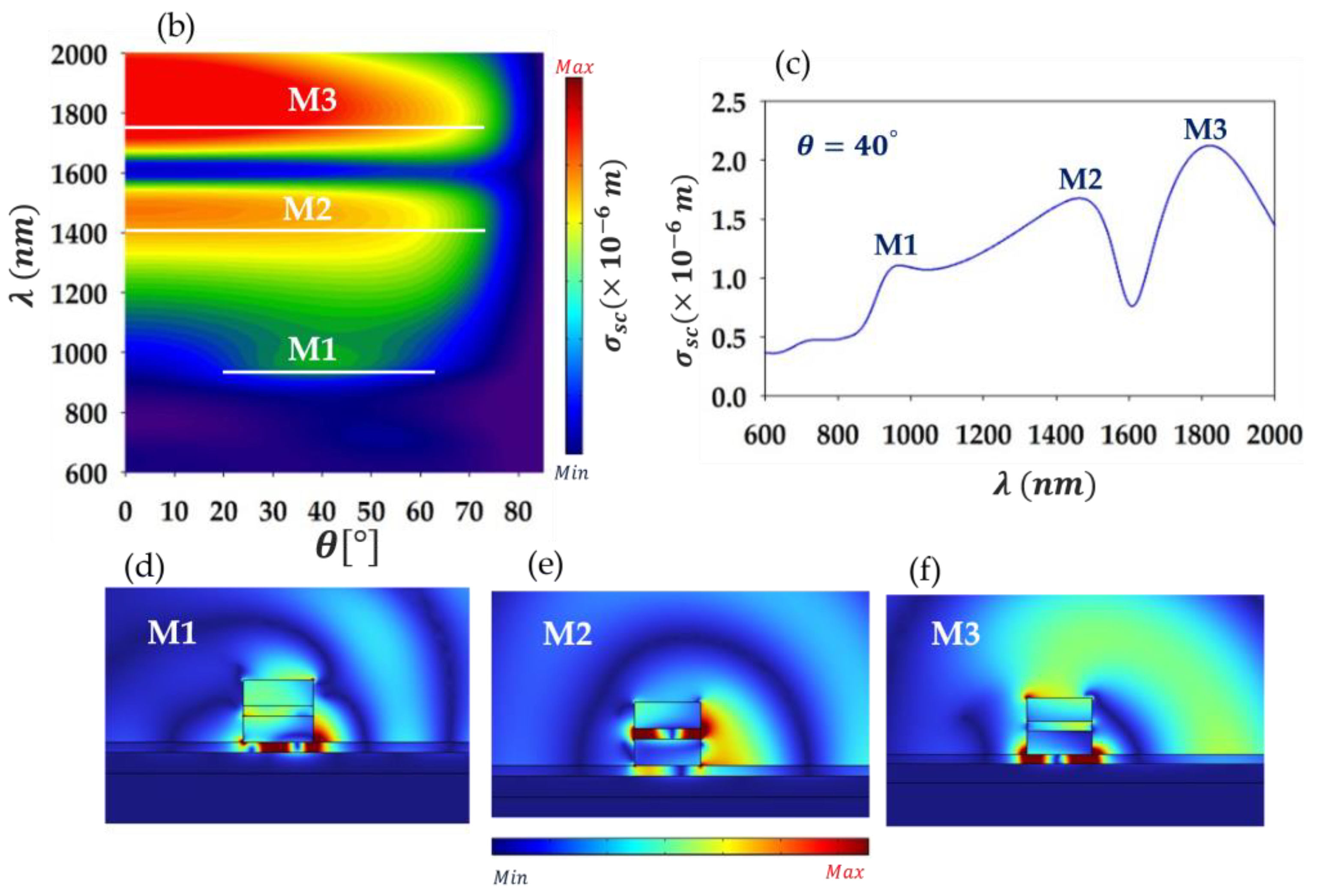
(a) Design of the 3D studied system composed of a gold nano-ridge with a thin polymer layer of thickness in the middle, placed above a gold layer with a polymer layer acting as a spacer in between. A zoom of the structure studied in 2D space is shown at the right side. (b) Simulated scattering cross section of the system in (a), as a function of wavelength λ and the angle of incidence . (c) Same as in (b), but for the fixed incidence angle, .. (d)-(f) Field maps of the scattered electric field within and around the nano-ridge corresponding to modes M1, M2, and M3 shown in (c) at wavelengths ~975 nm, ~1493 nm, and ~1689 nm, respectively.
To obtain the dispersion relation of the system, we have simulated the scattering cross-section
as a function of both the angle of incidence in the range [
], and the wavelength in the range of interest [
], that covers the visible and near-infrared domains. The corresponding results are shown in
Figure 1b in color scale. Let us indicate that red color indicates maximum scattering intensity while blue indicates minimum (scattering) intensity. Three distinctive modes are observed, highlighted with horizontal white lines, as a guide for the eye. We refer to these modes as M1 for the lower wavelength (or higher frequency) mode, M2 for the middle wavelength mode and M3 for the higher wavelength mode. It is worth noting that modes M2 and M3 are excited for nearly all values of
, while mode M1 is only excited in the range of
θ between approximately
and
. To give an idea about the behavior of these modes in the scattering spectra,
Figure 1c shows
as a function of wavelength at
, indicating three peaks corresponding to LSPs resonances at wavelengths 975 nm (mode M1), 1493 nm (mode M2), and 1689 nm (mode M3).
Figure 1d–f display the maps of the scattered electric field at these wavelengths, respectively. The field localization shows the presence of two types of modes: one confined underneath the ridges (modes M1 and M3) and one at the middle of the ridge (mode M2). A common characteristic between the modes is the fact that they are trapped in between two metal materials within a dielectric, which suggests that they correspond to metal-insulator-metal (MIM) type modes. To explore in more details this aspect of the modes and their general behavior versus the key geometrical parameters, we analyzed the effect of the nano-ridge width in
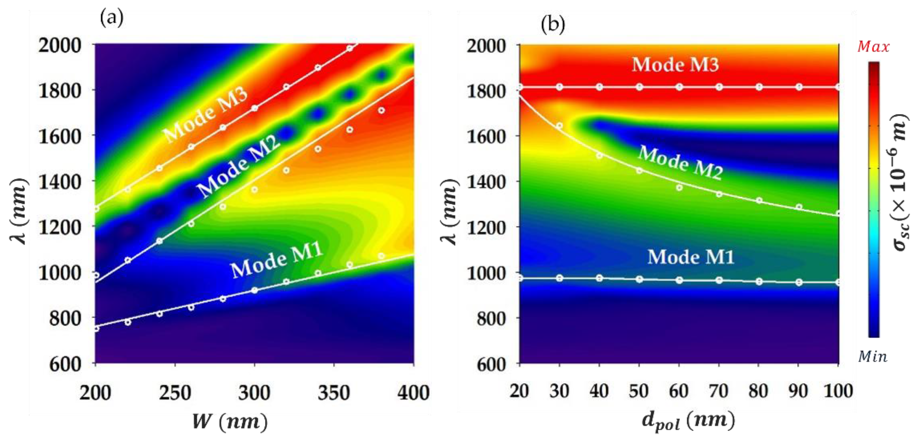
Figure 2a, where
is plotted as a function of both the wavelength and the nano-ridge width,
. The remaining parameters are kept as in
Figure 1, while the incidence angle is set to,
, ensuring the excitation of the three modes. One notes that the resonance wavelengths of the three modes (corresponding to the scattering maximum/peaks) increase linearly with the increase of W. This trend is typical in an effective plasmonic cavity acting as a Fabry- Pérot cavity, where MIM-type resonances correspond to confined plasmonic standing waves [
13,
30]. Accordingly, the thin dielectric layers either underneath or at the middle of the nano-ridge, where the modes are localized, acts as an effective plasmonic Fabry-Pérot cavity (PFPC) of nominal length
.
In particular, the plasmonic-MIM standing waves build-up due to reflections off the PFPC edges on each side. The resonance wavelength of the (plasmonic) modes can be expressed as [
30]:
where,
is the effective refractive index of the of the propagating MIM-like plasmon in the cavity,
is its wave vector,
is the wavevector in the vacuum, and
, 2, 3, … is an integer representing the mode number. This equation is derived from the resonance condition corresponding to a round-trip of the wave in the cavity, namely,
, where
is the phase-shift due to the reflection off the edges of the nano-ridge, whose value can be approximated as
[
30], where
is the effective length extension of the mode off the nano-ridge edges. Therefore,
is actually replaced by the length,
. By fitting the LSP resonance wavelengths (shown with open white circles in
Figure 2a), we estimated
to be approximately
for mode M1,
for mode M2, and
for mode M3. As for the values of
for each mode, these can be determined from the plot of the localized field inside the PFPC along the
axis. From
Figure 1d–f, we can deduce that m = 2 for mode M1, while for modes M2 and M3 m = 1. The solid white lines in
Figure 2a represents the fits of the numerical data (white open circles) using Eq. (3). We observe using the PFPC model based on the latter equation, that we have successfully fitted the numerical results (
Figure 2a), which confirms the mechanism behind the LSPs modes, M1, M2 and M3 formation.
In order to better understand the physics behind these modes, we have examined in
Figure 2b the effect of the polymer layer thickness
in the middle of the nano-ridge, for
. The rest of the parameters are set similar to
Figure 1. Let us recall that the field is essentially confined inside the polymer layer for mode M2, whereas for modes M1 and M3 the field is localized underneath the ridge. This, means that only mode M2 should be sensitive to
, which is evident in
Figure 2b as only mode M2 is affected by changes in
. In particular, one remarks that the resonance wavelength of mode M2,
, drops nearly hyperbolically as
increases. This trend reminds us that of the effective refractive index (
) of a metal-insulator-metal type waveguide versus its width, whereby
changes as the inverse of the guide width
i.e.,
[
31]. This relationship can be exploited to explain the behavior of
versus
considering what we mentioned above namely, mode M2 (or M1/M3) arises out of the trapping of a MIM-type mode in an effective plasmonic cavity (in the form of a MIM-standing wave). Hence, the effective refractive index of such MIM-plasmonic modes should changes as
, which enables to estimate the resonance wavelength as:
where, C is a fitting parameter. Applying equation (3), we have fitted the numerically calculated (FEM) resonance wavelength of mode M2 in
Figure 2b. Note that modes M1 or M3 are not fitted given their insensitivity to
. The curve based on equation (3) is depicted in a white solid line while the FEM results are shown in white open circles; we can notice the very good agreement achieved. The fitting provided in
Figure 2 using equations (2) and (3), enables us to definitely validate the physical mechanism behind the formation of modes M1, M2 and M3, mentioned above.
3. Localized Surface Plasmons of Coupled Gold Nano-ridges (Dimer)
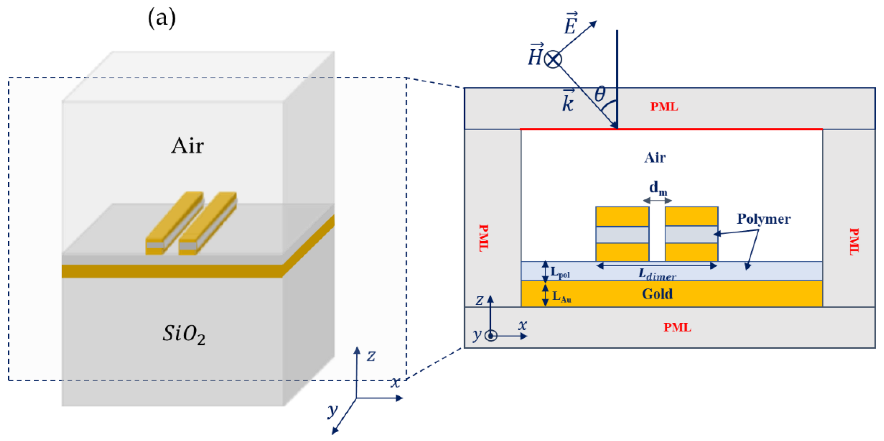
In this section, we investigate the effect of two identical coupled nano-ridges that form a dimer. This configuration is expected to enhance the localization of the plasmonic field and the quality factors of the modes, leading to stronger light-matter interaction [
13]. The two nano-ridges are set to be separated by a distance
, as shown in the 2D (x-z) plane of the simulated system in
Figure 3a. Note that
is a key parameter as it enables to control the coupling magnitude in-between the nano-ridges (forming the dimer).
Figure 3b, shows the simulated scattering cross section as a function of wavelength and incidence angle, with
, while the other parameters are set as earlier (
Figure 1). The plot reveals that for
, the modes are indistinguishable and not excited, but rather correspond to large scattering bands. However, for
, four modes labelled D1, D2, D3 and D4, show up. To examine these modes more closely,
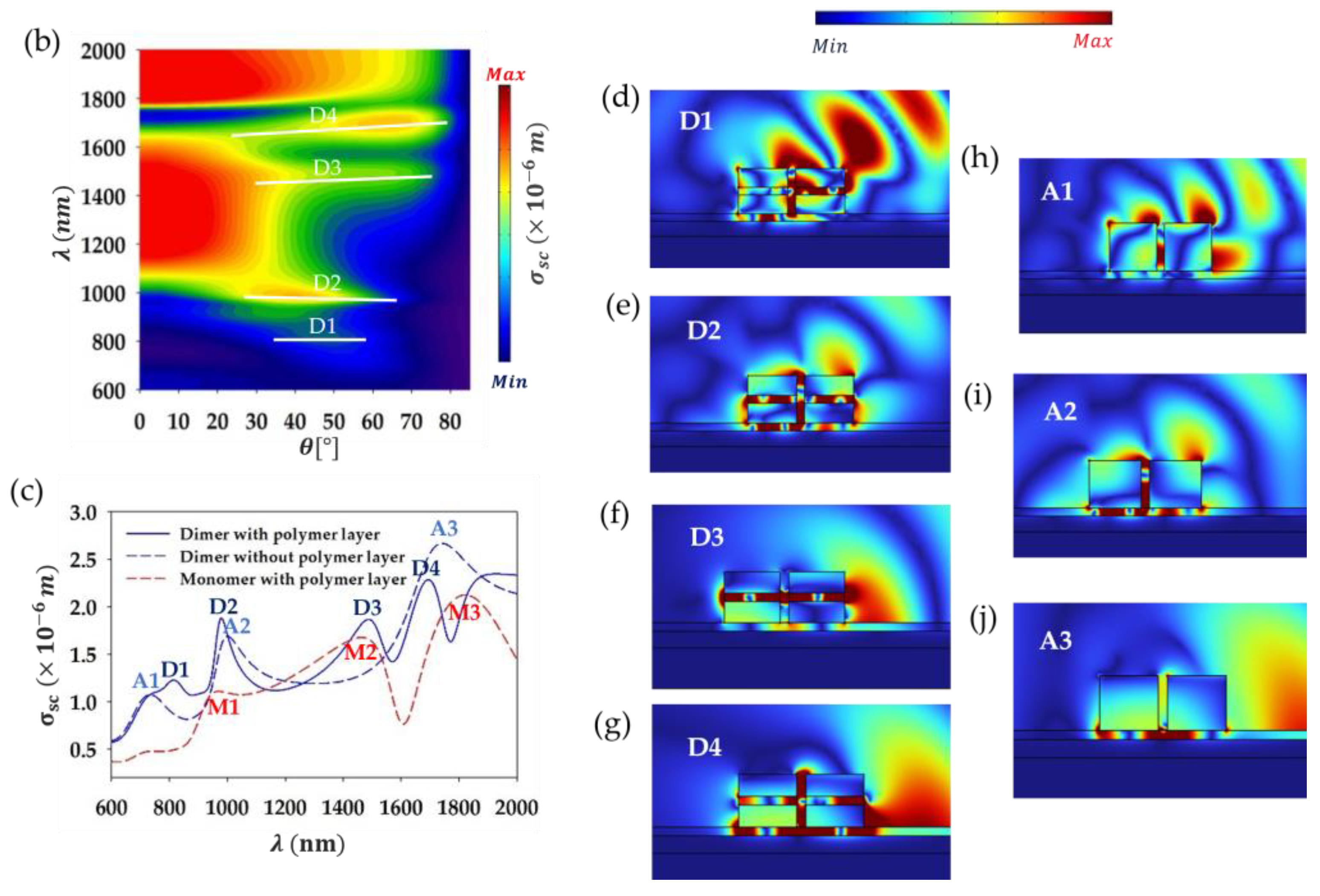
Figure 3c shows the scattering cross section at θ = 55° as a function of wavelength (blue line), where four peaks are clearly identified at roughly 816 nm (D1), 975 nm (D2), 1483 nm (D3), and 1690 nm (D4). A significant observation is that the quality factor of the modes in the dimer case is improved by approximately a factor of 3 compared to the single monomer case (red dashed line). For instance, if we focus on modes D3 and D4 which are the most strongly confined within the dimer, their quality factors are estimated as
and
, respectively. In comparison, mode M3 (of the monomer), which is the closest in terms of wavelength, has a quality factor of
. This improvement is attributed to the coupling between the ridges, which enhances the localization of the electric field as it is evident from the field maps of the scattered field shown in
Figure 4d–g. This enhanced localization is particularly evident for modes D2 and D4, where the field is strongly confined underneath and between the ridges, as well as inside the polymer layers in the middle of the ridges. For mode D2, the field is primarily localized in the polymer layers at the middle, but also in-between the ridges. In contrast, mode D1 exhibits weaker localization, having antenna-like components associated with multipolar localizations at the edges, that causes the field to radiate. Let us mention that the enhanced quality factor of the dimer modes comparing with the monomer case has been reported elsewhere [
13,
25]. As a matter of comparison, we have simulated the scattering cross section as a function of wavelength for θ=55°, for the dimer-structure without the polymer layer inserted in the middle of the ridges (blue dashed line). The curve is overlaid with that of a dimer (blue solid line) and monomer (red dashed line) structures with the polymer layer set in the middle as shown in
Figure 3c. We can observe that the insertion of the thin polymer layers within the dimer ridges results in improved quality factor of the modes. In addition, the spectrum is quite richer in the latter case as additional localized surface plasmons (with four modes) show up as compared to the case of no layers in the ridges (three modes). Furthermore, the localization of the field is significantly better with the polymer layer as seen in
Figure 3d–g, compared to the field maps in the case where no layer is inserted (
Figure 3h–j).
To analyze the impact of geometrical parameters on the dimer modes and the physical origin of the latters, we examine how variations in the width of the dimer
, and the thickness of the polymer layer in the middle of the ridges,
, affect the modes. The dimer width is defined as,
where
represents the single ridge width and
is the separation distance between the ridges. For the sake of simplicity, we alter
by changing only
and keeping
, that controls coupling intensity within the dimer, fixed. Also, all remaining parameters of the system are set equivalent to
Figure 1a (as mentioned above).
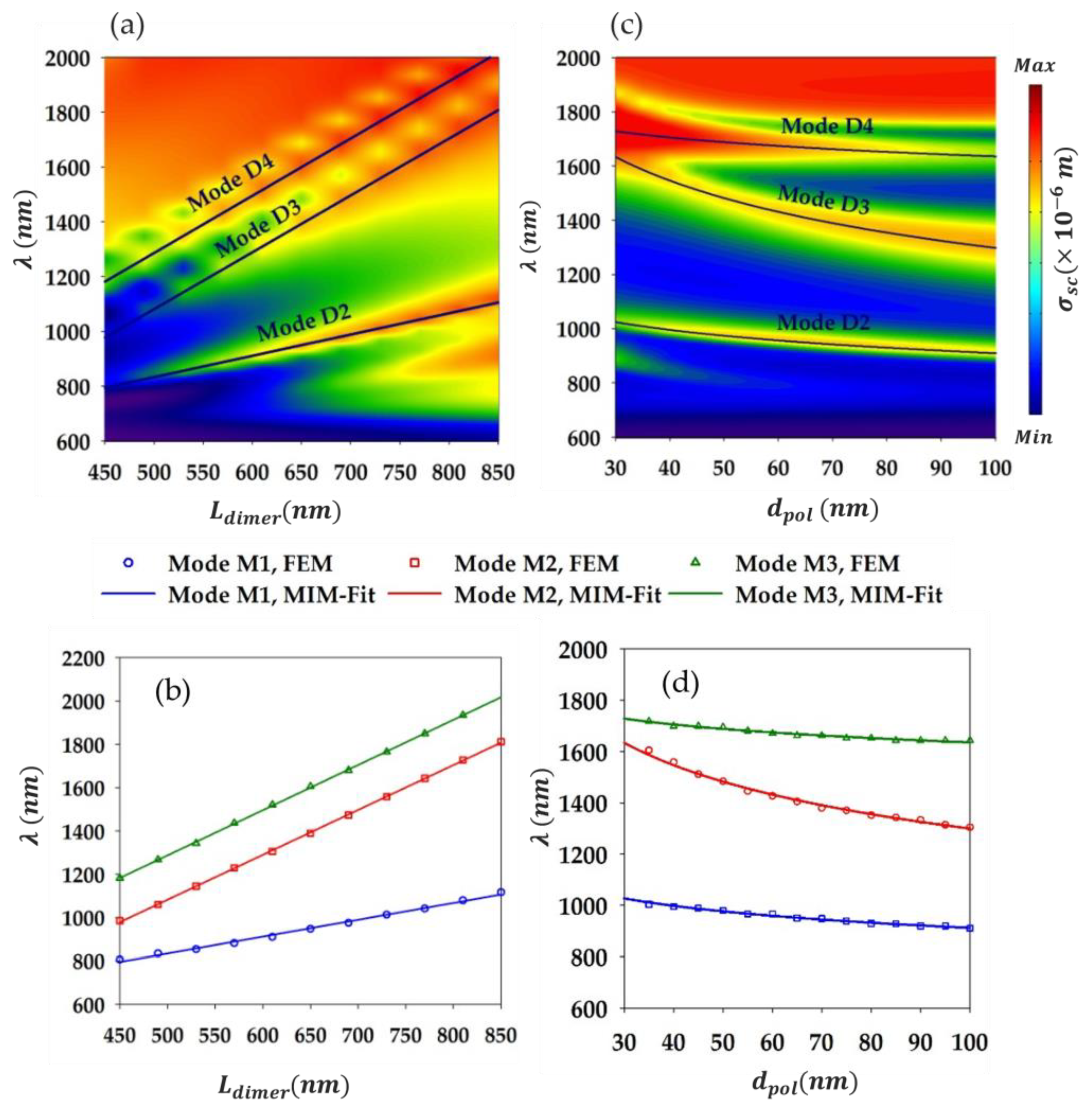
Figure 4a, presents the scattering cross section as a function of wavelength and
. We note a near linear redshift in the resonance wavelengths as
is increased, which is similar to what we observed above in case of the monomer (
Figure 2a) width increasing effect. This hints at the fact that modes, D1-D4, of the dimer could be considered as plasmonic MIM-type standing waves confined in an effective plasmonic cavity. The latter is either made of the thin layers in the middle of the ridges plus the small space in between (like for mode D3) or of the gap layer underneath the dimer, where mode D4 for instance is primarily localized. Let us call the latter cavity as the lower cavity, and the former as the upper cavity. Note that some modes (D1, D2 and D4) are confined in both the lower and upper cavities (with a different rate) as well as in-between the dimer. To confirm this, we consider that the MIM-type plasmonic standing waves corresponding to the modes are localized in either the lower or upper cavities (or both) of nominal length,
, and hence, the resonance wavelength is given by:
where all the parameters are defined in an equivalent manner as in Eq. (3) for the monomer. It should be stressed that the nominal length is replaced by,
, where the latter parameter is a fitting parameter. Such a parameter is meant to account for the mode extension off the dimer outer edges as already explained.
As for the modes order, m, it is determined based on the localized field in the effective plasmonic cavity (lower or upper). From
Figure 3d–g, we estimate m = 4 for the mode D2, m = 2 for both modes D3 and D4. We should mention that because mode D1 has complex features like antenna-like components, with no neat/simple localization features either in the lower or upper cavity, we do not consider fitting its resonance wavelength.
Figure 4b shows the fitting provided by Eq. (4) (solid lines) to the position of the modes D2, D3 and D4, resonance wavelengths (indicated by symbols) as a function of
. The fitting parameter
has been determined for each mode as: 58.35 nm for mode D2, 11 nm for mode D3, and 286.76 nm for mode D4. We note that the fitting agrees perfectly with the FEM results for all the three modes which clearly underscores the MIM-character of such modes, and that they correspond to MIM-type plasmon standing waves trapped in the effective lower/upper cavities.
We also explored the effect of varying the thickness of the polymer layers inserted in the middle of the ridges
.
Figure 4c shows the scattering cross section as a function of wavelength and
. This plot indicates that all modes are affected by changes in
, but the impact is significantly more pronounced for mode D3, which is understandable since mode D3 is primarily localized within such layers. Following mode D3, we see that mode D2 is the most affected as compared to mode D4, which is consistent with their field localization as the latter is more confined beneath the ridges than in their middle while for the former it is the opposite. Note that for mode D1 due to its complex features, it is difficult to analyze its behaviour versus changes in
, however, it can be remarked that for
, the mode is nearly cut-off as its scattering section becomes quite weak. For
, nevertheless, the mode shows a sensitivity with the increase of
as its wavelength drops with a non-negligeable magnitude, reflecting its localization in the (middle) layers. Using a similar equation to Eq. (4) and the same reasoning as in the case of the monomer, one can capture the modes, D3, D2 and D4 behaviour as
is changed. Equation (4) can be written in case of the dimer as,
, where the ridge width
is simply replaced by the dimer effective width,
, and
is a fitting parameter. Based on such equation, we provide the fitting of the three modes resonance wavelengths as a function of
in
Figure 4d, where we can observe the excellent agreement with the FEM results. Hence, we can be quite confident that modes D3, D2 and D4 arise out of the trapping of MIM-type surface plasmon guided mode in the lower/upper effective cavity, giving rise to resonating MIM plasmonic standing waves.
4. Effective Volume of the Dimer Localized Plasmon Modes and Prospective Optomechanical Coupling
Here, we focus on the analysis of the effective mode volume of the localized surface plasmon modes of the dimer, aiming to classify these modes for an optimal enhanced optomechanical coupling with localized phonons supported by the dimer. As a matter of fact, the present study which is about a thorough analysis of the plasmonic properties of the dimer-based device, comes after a previous study about phononic characteristics of the system [
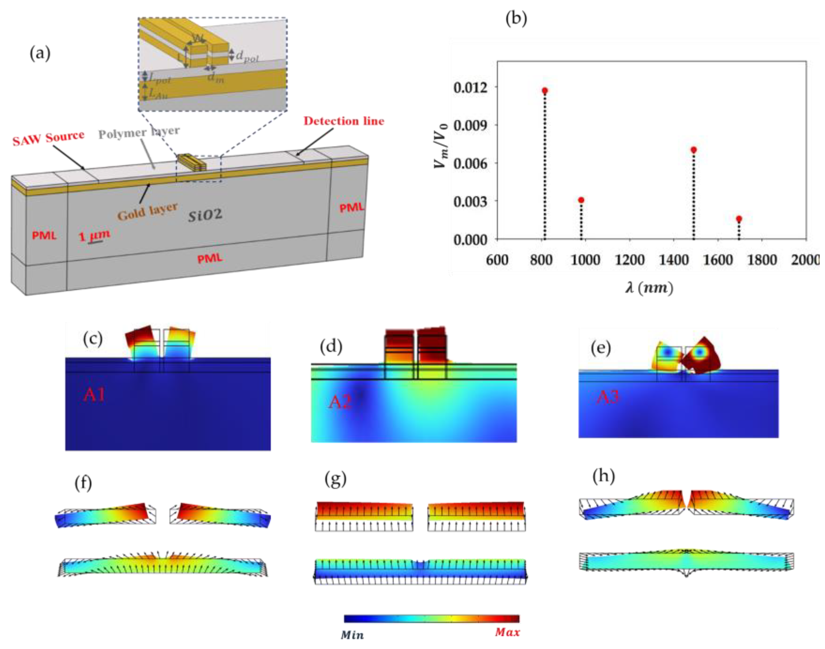
27]. The general realm being to achieve enhanced plasmon-phonon coupling using surface acoustic waves (
Figure 5a). In that framework, we would like to provide in this last paragraph a prospective qualitative analysis of enhanced optomechanical coupling harnessing the dimer plasmonic modes effective volume. Note that the optical mode volume is one of the key parameters that govern light-matter interactions in general, as it is related to field enhancement and spatial localization [
32,
33]. Having an estimation of the effective mode volume can help quantify the spatial extent of the electromagnetic energy confinement, directly impacting the interaction strength between light and matter. To get an estimate of the effective mode volumes
, we use the quasi-static approximation to calculate the mode-volume integral for a leaky plasmonic cavity given [
34,
35,
36]:
where, the integral is performed over of the volume (surface times unit length) of both nano-ridges,
is the electromagnetic energy density and max
is its maximum value in the simulation domain. For a dielectric medium, the energy density takes the simple form,
, while in the case of a dispersive and lossy medium like a metal, an appropriate relation is as follows [
31]:
where,
is the complex dielectric function of the metal. In our case, the latter is given by the Lorentz-Drude model (Eq. 1).
on the other hand, is the mode damping taken as the linewidth of the respective LSP mode. As already mentioned, the simulation is performed in 2D due to symmetry along y-axis, so to calculate the mode volume one should perform surface integrals in the 2D-cross section system, and then multiply the result by a unit length along the y-direction.
Figure 5b, shows the normalized effective mode volume
calculated for each mode of the dimer (D1, D2, D3 and D4), where
(
), is the volume occupied by the associated resonance wavelength of the mode in the polymer layer. As can be seen, the effective volumes of modes are well below
, reflecting the strong confinement of the dimer plasmonic modes far below diffraction limit of light. From the values of the mode volumes, we observe that mode D1 has the largest value of
, indicating relatively lower field localization rate compared to the other modes. This relates to such mode localization features like its tendency to radiate energy, due to its antenna-like components associated with multipolar localizations at the edges. In contrast, mode D4 with the lowest value of
, is relatively the most strongly confined mode. Mode D2 and D3 fall in-between with values
and
respectively. This result shows that for enhanced light-matter coupling purposes, mode D4 should offer the highest interaction rate as the coherent coupling rate between light and matter scales as
[
36].
Regarding the optomechanical coupling specifically, we can affirm that the plasmon-phonon interaction is qualitatively related to the overlap degree between the plasmon and the phonon in a given cavity. This is estimated quantitively via the so-called optomechanical coefficient whose expression is determined based on the photoelastic volume and the surface moving-boundary effects [
13,
37]. Given that the dimer plasmonic modes with the lowest volume magnitude
are the most highly trapped plasmons, they should manifest the higher overlap rate with a given phonon localized in the dimer. As a result, such modes should lead to an optimal optomechanical coupling intensity. In
Figure 5c–h, we recall the localized phonons of the dimer that we deemed to be optomechanically active based on symmetry arguments in a previous work [
27], and the design enabling to use surface acoustic waves to excite such phonons. Considering for instance the in-phase compression mode A2 (
Figure 5d), that deforms the polymer layers both under and in the middle of the ridges (see
Figure 5g), where modes D2, D3 and D4 are localized, we can roughly classify such modes (based on their volume) in terms of optomechanical coupling rate
as:
The same reasoning approximately applies if we consider another phonon of the dimer, to classify the LSPs modes in terms of acousto-plasmonic coupling magnitude. Obviously, a thorough study based on the rigorous simulations of the optomechanical coefficient is needed to determine the best localized phonons and plasmons that yield the highest coupling magnitude. However, this qualitative argument based on the modes volume gives already a good hint regarding the most promising plasmonic mode for the enhanced optomechanical purpose namely, mode D4 that shows the lowest volume or equivalently the highest confinement rate.
