1. Introduction
Wide bandgap (WBG) power semiconductor devices based on silicon carbide (SiC) and Gallium nitride (GaN) are very attractive in high-power applications because of the significantly reduced losses compared with their Si counterparts. They are now being commercially introduced at various voltage and current ratings, enabling power conversion applications from kilowatts to megawatts in solar and wind, battery energy storage systems, smart grids, electric vehicles, data centers, consumer electronics, and so on [C1-C3].
Due to the superior capability of these devices, researchers with limited resources or experience can also develop very high-power converter prototypes. However, once the high-power converter is designed and assembled, evaluating the hardware design becomes challenging because it requires many lab resources such as high-power DC and AC power supplies, heavy-duty resistive loads, and facility electric grid capacity. Also, if tested using resistive load, the test could result in substantial energy waste. For example, the power consumed running a 100kW resistive load test for one hour may be enough to supply a typical US household for 3-4 days. So, there is a need to validate the WBG high-power converters with higher energy efficiency and with limited lab resources.
The Power Electronics Power Stage (PEPS) is the most critical part of a high-power converter, which generally incorporates power semiconductor devices, the busbar, gate driving circuits, and thermal management components.
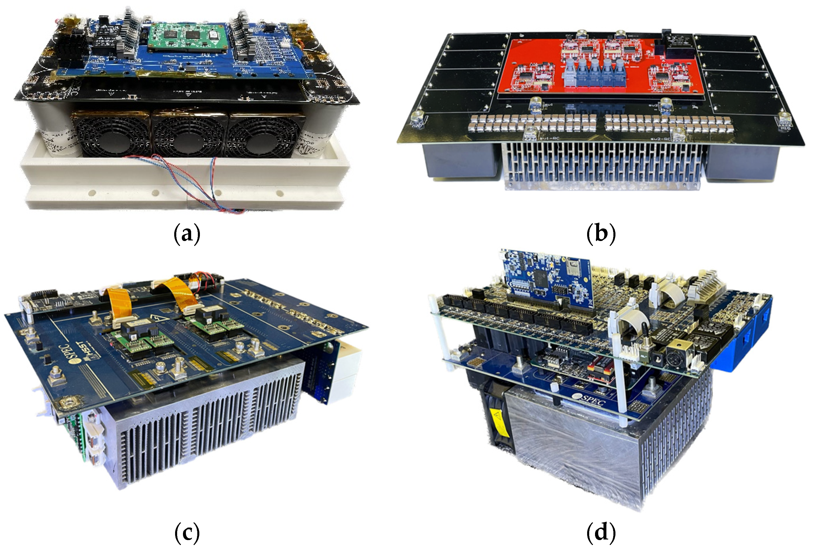
Figure 1 illustrates a few examples of SiC high-power WBG PEPS developed. These PEPSs are fundamental units for high-power WBG converters deployed across diverse applications, including grid-forming PV systems, intelligent grid-tied converters, and electric vehicle DC fast chargers [C4-C6].
This paper outlines the testing methodology employed by the authors to evaluate the high power WBG PEPS hardware. The proposed evaluation methods are summarized in
Figure 2. The comprehensive testing approach assesses critical aspects, including switching characteristics, driving circuit functionality, thermal management performance, insulation levels, and continuous operation at full power capacity. We utilize the double pulse test (DPT) to characterize the power semiconductor switching behavior, extract parasitic parameters, and validate the magnetics. Furthermore, the DPT serves to optimize gate driving circuits, validate overcurrent protection mechanisms, and measure device on-resistance. In addition to the DPT, we introduce multicycle tests designed to evaluate steady-state performance and estimate efficiency swiftly. Our testing methods extend to experimental verification of key thermal parameters, recognizing the critical importance of thermal management in high-power/high-voltage converters. This verification includes junction-to-ambient thermal resistance and thermal capacitance extraction through heat loss injection. A correlation method between temperature sensor measurements and junction temperature is presented to enhance the accuracy of device temperature monitoring during tests.
To ensure the insulation reliability of the converters, our methodology incorporates dielectric withstand tests and partial discharge measurements. These tests serve to verify insulation integrity at both component and system levels. Finally, we underscore the significance of testing converters under full voltage, current, and thermal conditions in power circulation tests. These testing methodologies enable a comprehensive evaluation of the converter’s thermal management, testing it to its maximum voltage/current/thermal rating and estimating its efficiency while placing minimal requirements on the power supply, load, passive components, and facility electric grid capacity. These testing methodologies are universally applicable to all high-power converters except where the semiconductor and packaging difference between Si and SiC devices stands out.
2. Switching Characteristics Evaluation
2.1. Double Pulse Test Using the Two-Level Phase Leg Switching Cell
The Double Pulse Test (DPT) is widely used to evaluate the device’s switching performance, extract parasitic inductance, validate the gate signal integrity, tune the gate driving circuits, and verify the over-current protection function. A typical DPT test setup is shown in
Figure 3. One of the two semiconductors is the device under test (DUT); it can be the top switch or the bottom switch. Since the top switch typically has a much worse common mode noise problem, it is recommended to test the top switch to ensure the integrity of the converter and the gate drive circuit’s ability to suppress the noise and false trigger. The other switch in the DPT is parallel to an inductor and acts as the freewheeling switch. Compared with using a freewheeling diode, the freewheeling switch can use the same device as the DUT and works in the third quadrant as a synchronous rectifier, mimicking the operation condition of a real converter. An accurate positive/negative gate driving voltage is also necessary since it changes the device’s properties. The DPT is suggested to be tested at least 1.5X current rating at designed bus voltage in case of corner case in system operation. The inductor’s saturation current needs to be higher than the maximum current in the DPT, so using an air-core inductor is a good practice for the DPT. The turn-to-turn capacitance of the inductor can bring an undesired oscillation hence needs to be minimized. The DPT can also operate with the real magnetics to be used in the system, such as the boost inductor, or short the secondary side of transformer and work as an inductor; however, the current will be limited by saturation. Once the inductor is constructed and characterized, changing the DUT conduction time T
s can tune the switching current at a certain bus voltage. The pulse energy is mainly from the DC link capacitor C
DC. Thus, the power supply can set a less than 1A current limitation, or an additional contactor, S
1, can be added to disconnect the setup from the power supply after the capacitor bank is charged. Adding energy release resistor RB and contactor S
2 is optional for safety purposes.
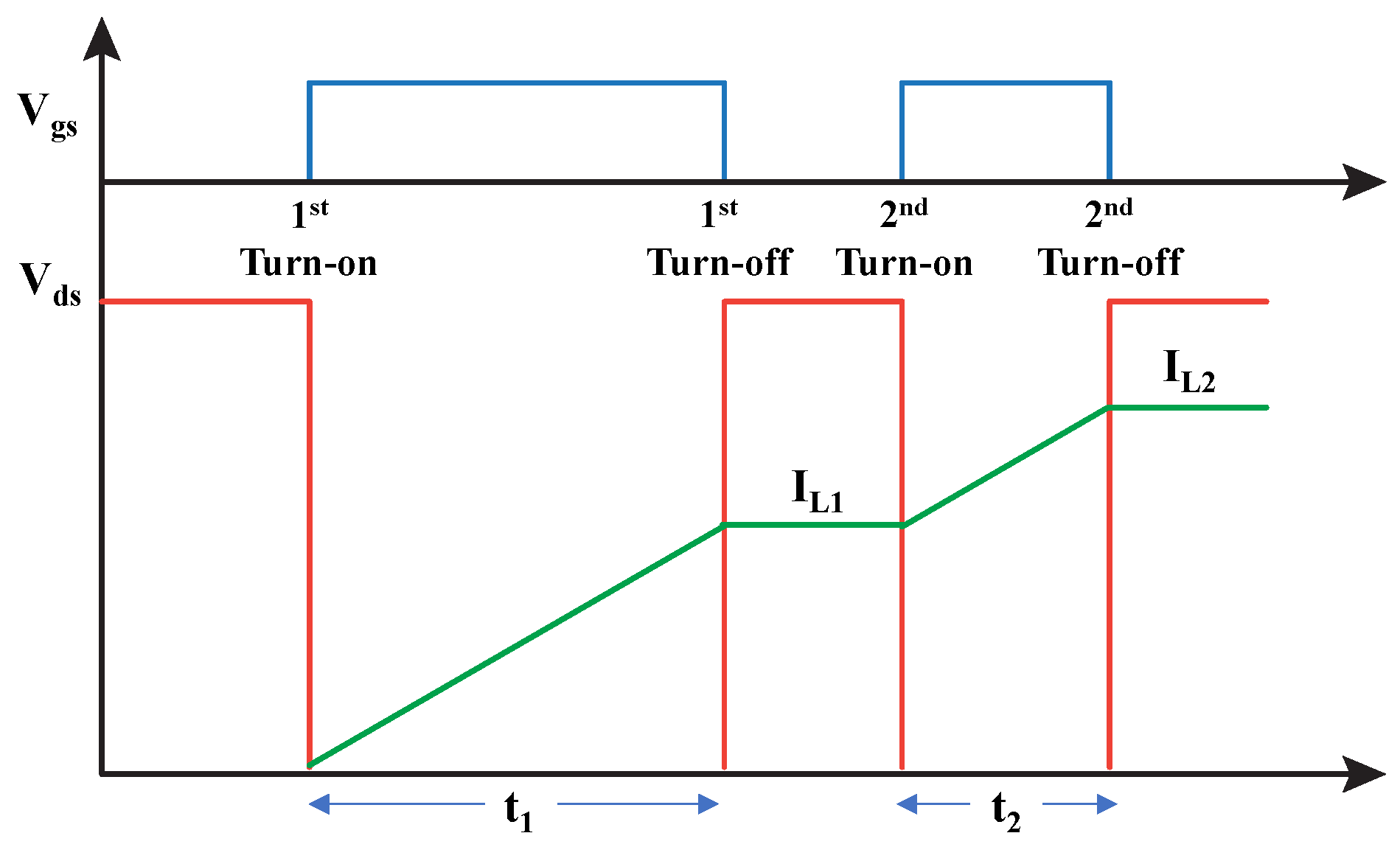
A typical double pulse test waveform is presented in
Figure 4. The desired switching current can be set by adjusting the pulse width t
1 and t
2. The inductor current after each pulse can be calculated by Equations (1) and (2). Four switching points can be captured, which are turning on at zero load current; turning off at I
L1; turning on at I
L1; and turning off at I
L2. In most cases, turning on/off at I
L1 is the test objective, so the second pulse t
2 should be as short as possible to avoid the undesired high turn-off current I
L2. This characterization therefore mimics the switching performance of a hard switching converter.
In the DPT, the first turn-on happens at zero load current. Since the load current is zero, the measured DUT current represents the freewheeling switch’s reverse current when it is charged from zero volts to the full voltage. This feature can be used to estimate the freewheeling switch’s capacitance Coss and stored charge Qoss. The accuracy of this measurement is affected by the parasitic capacitance of the PCB board and the load inductor. So having the load inductor capacitance characterized separately is needed in order to improve the accuracy of the Qoss measurement.
Since WBG power devices are much faster, a decoupling DC capacitor placed very close to the device is desirable to minimize the device voltage overshoot during the turn-off switching. The decoupling capacitor is recommended to be larger than 250 times the device’s internal C
oss in [C7]; a lower ESL is also desired for better performance. The main DC-link capacitor C
DC also needs enough capacitance to ensure each switching dynamic happens at the same voltage; otherwise, the bus voltage will drop, and the second pulse is not characterized at a lower voltage, especially when a current is very high. The parasitic inductance in the entire power commutation loop greatly influences the switching waveform; a higher loop inductance will contribute to a higher voltage overshoot during the turn-off transients. The power loop inductance L
p can also be quickly calculated by Equation (3); the C
PCB and C
probe are the parasitics induced by the PCB and probes. The
is the resonance frequency after turn-off.
The measurement equipment and correct probe connection points are also critical in the DPT test. The voltage and current measurement equipment must have sufficient bandwidth to capture the high-resolution waveform that can then be used to calculate the switching losses. The equivalent bandwidth of the rising edge and falling edge can be estimated by the rising time (tr) and falling time (tf) as , and the measurement system bandwidth should be at least 3-5 times higher than the maximum equivalent bandwidth of the switching events [C8]. A coaxial shunt resistor is claimed to be a high bandwidth solution [C9-C10]; still, it will increase the loop inductance by at least 2.2nH, nearly 10% of the total loop inductance for optimized TO-247 based SiC converters, or even 100% for surface mount GaN device based converters. A non-invasive current measurement, such as a Rogowski coil probe is desired. The lower bandwidth of an off-the-shelf Rogowski coil is the downside for very fast switching cases. Some high-bandwidth Rogowski coils have been researched but not commercialized [C11-C12]. Rogowski coil can be used in a converter hardware setup where the footprint for the coaxial shunt resistor does not exist. However, the measurement result might be compromised if a high-current conductor (such as the inductor terminal) is placed nearby. Additionally, the bandwidth and size of Rogowski coils are often limited by the availability of commercial options on the market.
Alignment for V/I measurement is essential in loss calculation since a slight difference in probes’ propagation delay can cause a significant switching loss calculation error. For example, a 1ns delay can generate over 80% measurement error with a fast-switching WBG device [C8]. Many of the V-I misalignment methods require additional calibration fixtures or components, thus directly de-skewed by using the DPT waveform is very attractive [C13]. The fast-rising device current will cause a voltage dip on V
ds during the turn-on, where ΔV=L
p*(dI/dt). The V
ds and Id can be aligned using two points, the starting point of the V
ds decay should match with the current rise, and the maximum I
d matching with the maximum voltage dip. A detailed example of V/I alignment is given in the next section with experimental waveforms in
Figure 6.
2.2. Understanding Double Pulse Test Waveform
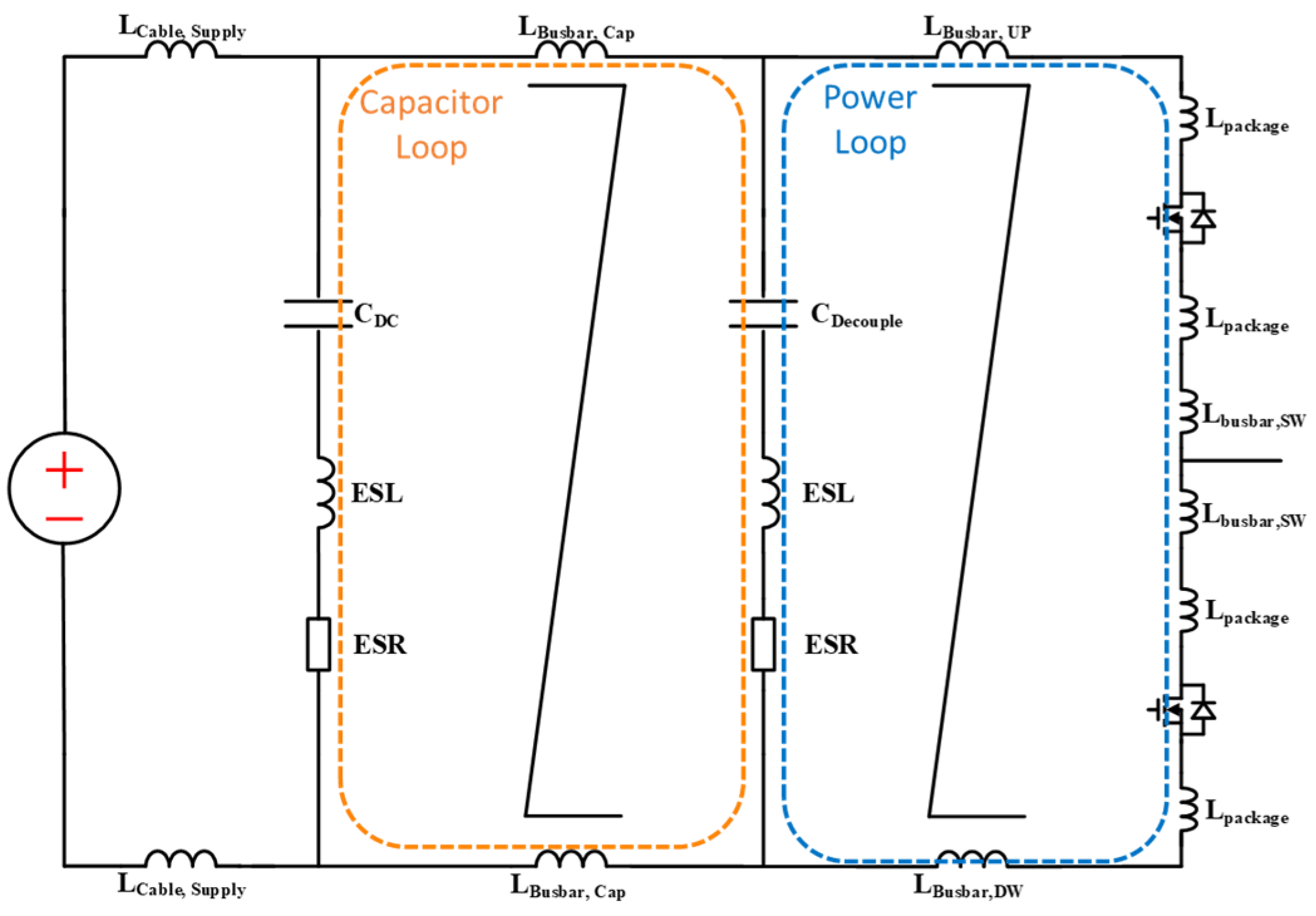
In a complete converter with a large DC link capacitor, two loops are actually formed as shown in
Figure 5. One is the inner power loop that defines the overshoot voltage and switching loss; the other is the capacitor loop between the low-value decoupling capacitor and the bulky DC link capacitor. The power loop inductance includes the device’s internal inductance, mainly determined by the lead and bond wire, and the external inductance, the loop inductance on the busbar. As shown in
Figure 5, the power loop introduces a high-frequency oscillation during device switching, and the capacitor loop brings in a lower-frequency oscillation between the decoupling capacitor and the DC link capacitor.
Figure 5.
Commutation loop inductance.
Figure 5.
Commutation loop inductance.
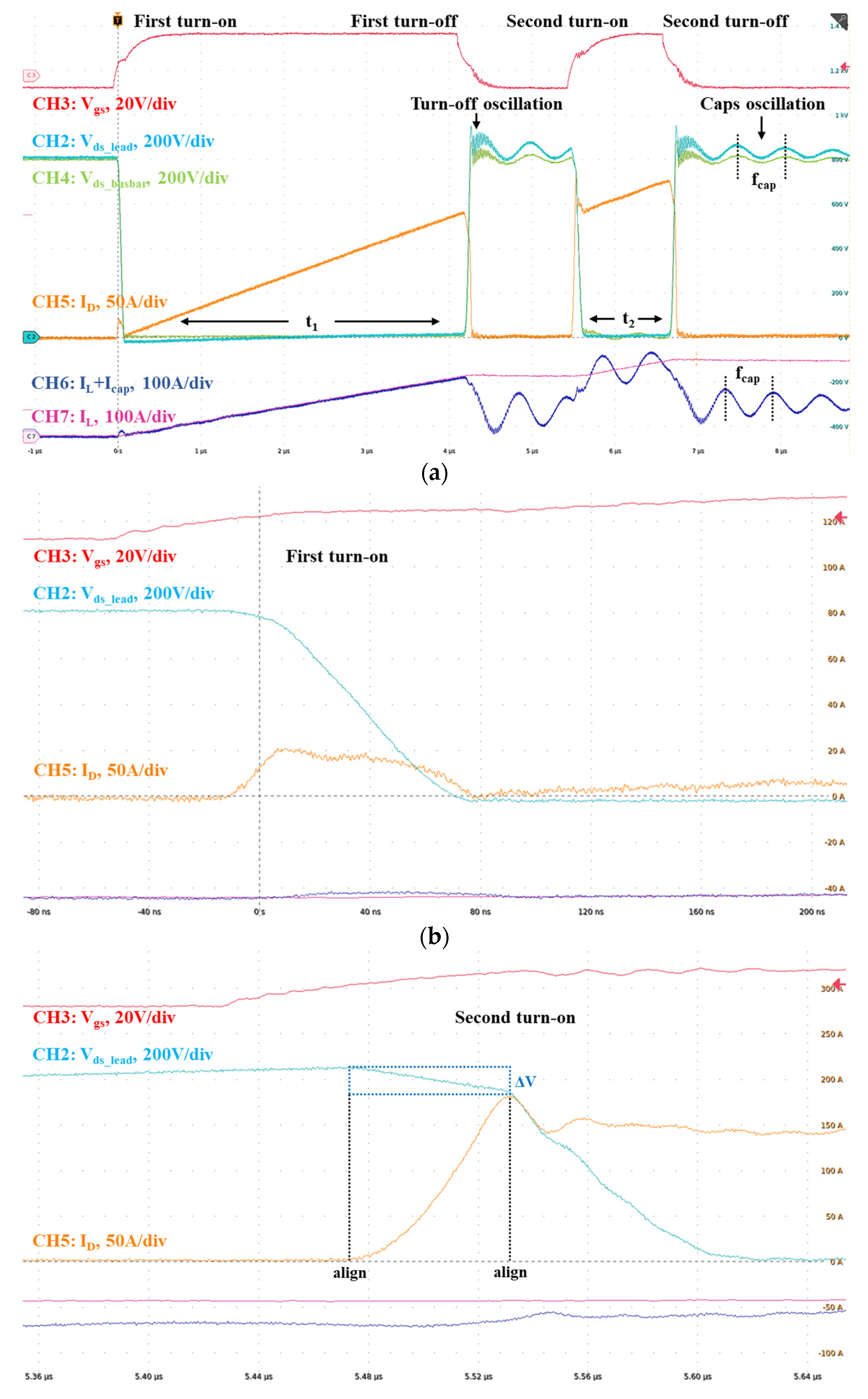
A typical bottom-side DUT DPT waveform is given in
Figure 6, where a TO-247 packaged SiC MOSFET (Infineon IMZA120R007M1H) is tested at 800V and up to 175A. CH3 is the V
gs of the DUT. CH2 shows the drain-source voltage for the DUT directly measured on the lead (closest point to the die in the MOSFET package); CH2 is measured by 800MHz passive probe TPP0850. CH4 also shows the drain-source voltage for the DUT but is measured on the power terminals on the busbar, which is relatively far away from the die; CH4 is measured by 200MHz differential probe THDP0200. CH5 is the drain current where a 30MHz Rogowski current probe TRCP0300 is placed around the drain lead of the MOSFET. CH7 presents the current on the inductor, measured by TCP0150. CH6 measures the current in the capacitor loop, which is the sum of the MOSFET drain current and the current goes into the decoupling capacitors; CH6 is measured by the Rogowski current probe.
Figure 6a clearly shows the measured V
ds during turn-off is significantly lower if the measurement point is far from the die in the MOSFET package. This result also suggests that measuring the V
ds of a SiC power module is less accurate since the power module’s drain terminal is far from the die inside the module. Actual device stress is higher.
Figure 6.
Typical switching waveform for double pulse test. (a) Double pulse test with 800V bus voltage. (b) Zoom-in waveform for the first turn-on at 0A. (c) Zoom-in waveform for the second turn-on at 138A. (d) Zoom-in waveform for the second turn-off at 175A.
Figure 6.
Typical switching waveform for double pulse test. (a) Double pulse test with 800V bus voltage. (b) Zoom-in waveform for the first turn-on at 0A. (c) Zoom-in waveform for the second turn-on at 138A. (d) Zoom-in waveform for the second turn-off at 175A.
Figure 6b illustrates the waveform for the first turn-on; it can validate the switching characteristics for soft switching topologies and measure the real Q
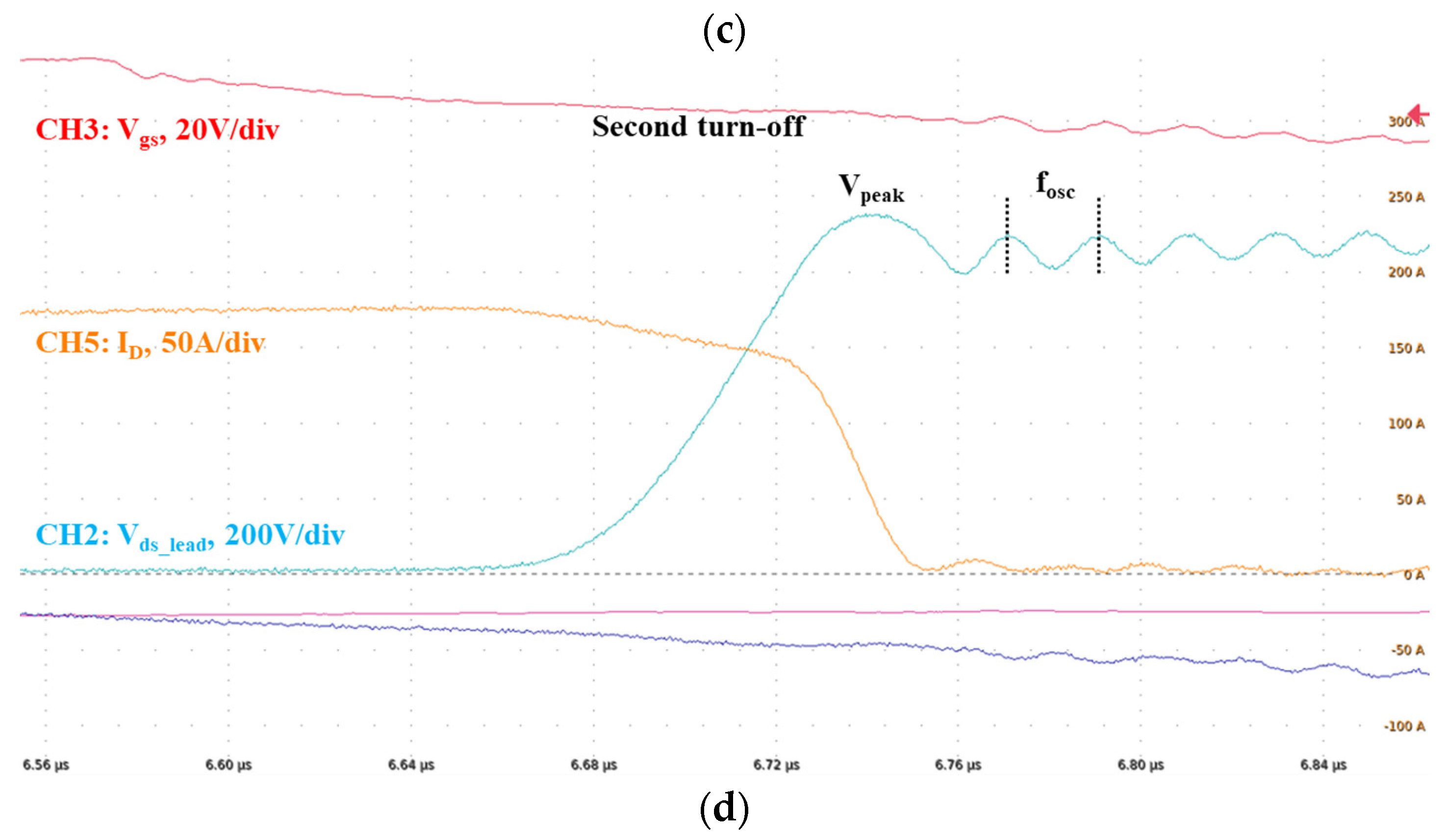
oss by integrating the measured current. The V-I measurements can be deskewed using the second turn-on waveform under a heavier load condition, as is shown in
Figure 6c.
Figure 6d shows the second turn-off where the highest overshoot voltage is present. The switching loss during the turn-on and turn-off can be calculated by integrating the V-I overlap during the switching transient. The gate resistance can also be optimized using the double pulse test, trading off between the switching speed, loss, overshoot voltage, gate loop stability, and EMI.
Numerous research studied the power loop inductance extraction methodologies,
The loop inductance can be accurately extracted by Q3D simulation, measured by equipment, or experimentally tested [C14-C17]. Extracting power loop inductance and capacitor loop inductance can be extracted through the DPT waveform is very attractive because of its easy implementation. Using the DPT waveform in
Figure 6 as an example, the turn-off resonant frequency f
osc is measured to be 51.4 MHz, the SiC MOSFET C
oss is 420pF from the datasheet, ignore all other parasitic and using Equation (3), the power loop inductance is estimated to be 22.8 nH. It can be revalidated using the V
ds voltage dip during the second turn-on or overshoot voltage at the second turn-off. As shown in
Figure 6d, the maximum dI/dt is measured to be 6.9A/ns, the overshoot voltage is 154V, L
p is calculated to be 22.3nH by ΔV=L
p*(dI/dt). Similar results are shown in
Figure 6c, where the maximum dI/dt is measured to be 4.6A/ns while the V
ds dip is 102.8V, and the L
p is calculated to be 22.3nH. These three methods get similar results despite measurement error, ignored parasitic capacitance, and inaccurate C
oss. The capacitor loop inductance can also be extracted using the decoupling capacitor value and oscillation frequency f
cap. For example, in
Figure 6a the capacitor loop inductance is estimated to be 22.2nH with 408nF decoupling capacitor and 1.69MHz resonant frequency.
2.3. Multicycle Test
The Multicycle Test (MCT) is an essential step for powering up the converter after evaluating the switching performance in the DPT. In the MCT, the complete converter is connected to a resistive load and runs at the rated voltage and current for several line cycles (60Hz for grid-connected or a few kHz for motor drives). Limiting the number of cycles to small, such as 5-100 line cycles, means no need to worry about heating the load or the converter (using thermal capacitance). The converter may not need to be attached to a fully functioning cooling system. The number of cycles needs to be small, so device heating is not a concern. The MCT can provide validation of the auxiliary voltage power supply unit and driving circuit reliability since the switching pulse number is significantly increased over the DPT (e.g., ten 60Hz line cycles contain 10k pulses at a 60kHz switching frequency). False turn-on/off of the switch and shoot-through should be checked during this stage.
An MCT test example is in [C18-C19]: a 500kW inverter is tested to full voltage/current rating while connected to a kW level resistive load and running 5 line cycles. The converter’s efficiency can be estimated by integrating the data from the oscilloscope. However, this efficiency is the upper limit of the converter’s real efficiency because the operating temperature is close to the room temperature. Once the converter runs continuously and heats up in the steady state, the semiconductor conduction loss and switching loss will increase, and many other passive components and traces will also all become lossy, reducing the steady state efficiency.
2.4. Functionality Validation
Smart functionalities integrated into a PEPS have been extensively researched and are suggested to be a necessary feature for high-power WBG converters [C20-C21]. These functions include protection circuits, temperature sensing, current sensing, voltage sensing, and online health monitoring. Validating these functions can also take advantage of the DPT’s flexible voltage and current control.
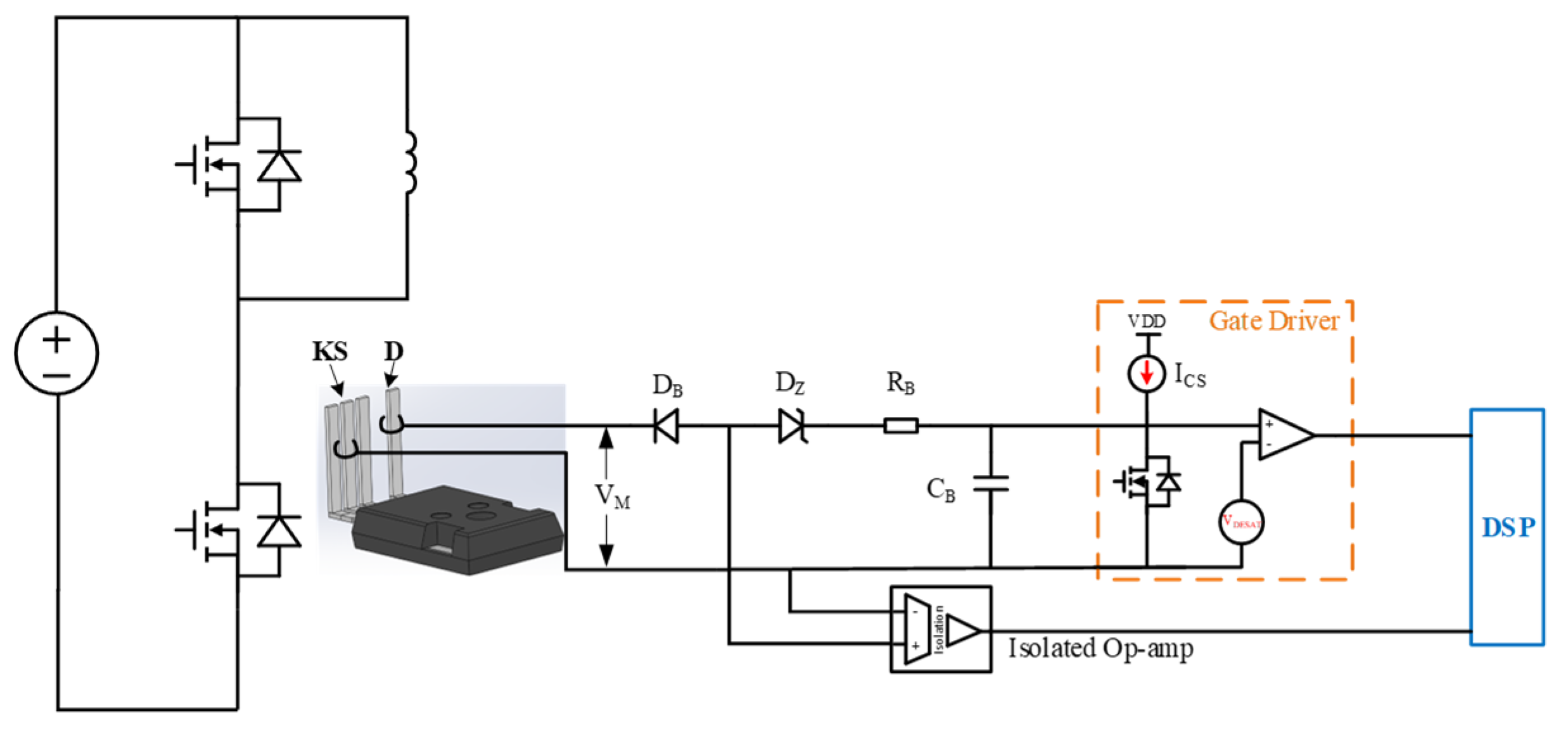
Figure 7 presents an online voltage measurement and over-current (OC) protection circuit [C22]; the circuit consists of a gate driver internal current source, a low-voltage Zener diode D
Z, and a high-voltage Schottky diode D
B.
The protection current threshold can be calculated by Equation (4), where V
DESAT is the comparator voltage inside the gate driver, and I
CS is the current source current. The measurement voltage V
M can be represented by Equation (5), where V
DB is the diode D
B voltage.
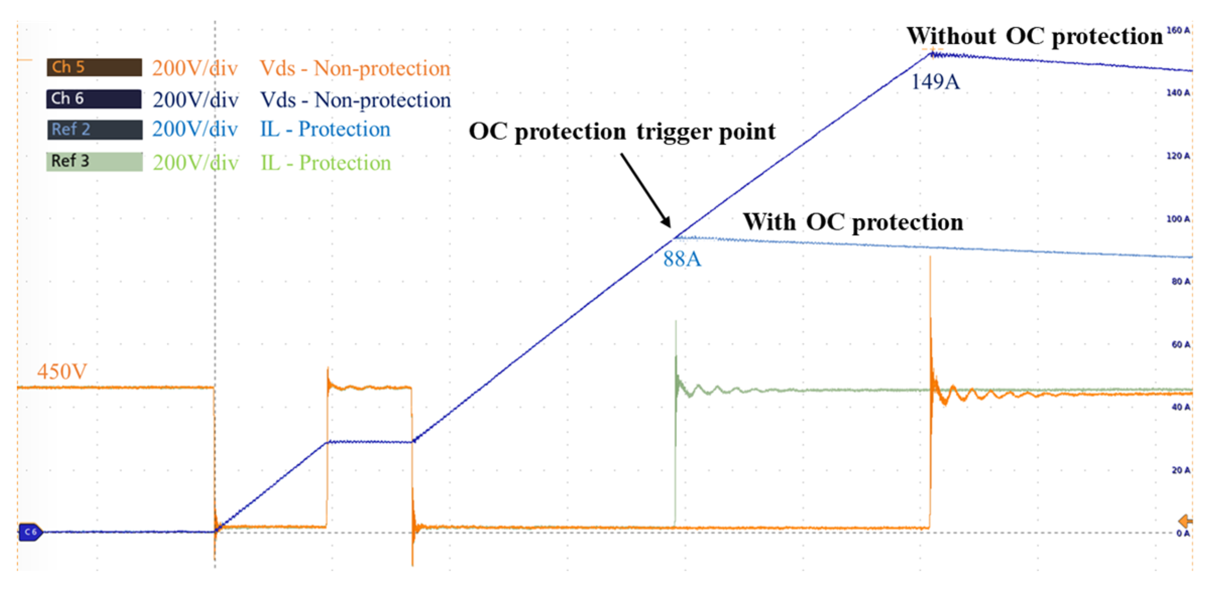
Figure 8 presents verifying the overcurrent protection function in a DPT. The overcurrent protection is triggered at 88A, while the current goes to 149A (determined by t
2 as shown in
Figure 4) if the overcurrent protection is disabled.
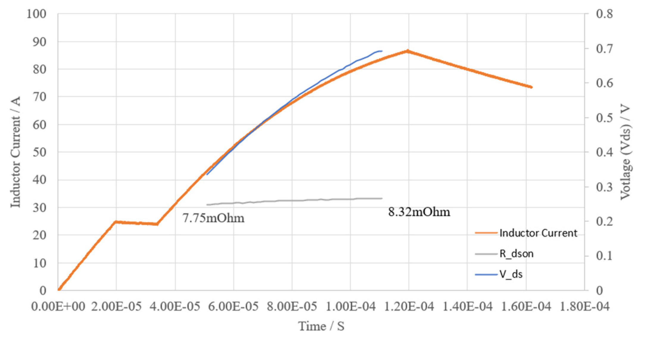
The device’s on-resistance can also be extracted during the DPT by using the circuits shown in
Figure 7. The Digital Signal Processor (DSP) reads 50 VM samples in a DPT. The results are plotted with the device current measured by the TCP0150 current probe, as shown in
Figure 9. The on-resistance can then be calculated as 7.8mΩ to 8.3mΩ at 24
oC room temperature, matching well with the datasheet (UnitedSiC UF3SC120009K4S).
3. Thermal Management Evaluation
3.1. Heat Injection for Thermal Management Evaluation
Thermal management defines a high-power converter’s current and power rating; evaluating the thermal performance is necessary before any high-power continuous test. The thermal impedance can be modeled by a thermal network equivalent circuit model, such as the Cauer model, also known as the Continued-fraction circuit (
Figure 10a), and the Foster model, also known as the Partial-fraction circuit (
Figure 10b). The Cauer model reflects the physical setup of the thermal resistance and thermal capacitances. In contrast, the Foster model is an analytical model for thermal parameters calculation; individual RC elements of the Foster model do not represent the layer sequence, and the network nodes do not have any physical correlation [C23-C24].
To evaluate the thermal performance, the easiest way to generate a fixed amount of heat is to inject current in the reverse conduction direction of the converter by swapping the connection with the DC busbar (
Figure 11a); all the phase legs across the same busbar will be paralleled in reverse conduction. This method works well with SiC and GaN devices since they all include an internal body diode. This method does not work for the Si IGBT or SiC module with antiparallel diodes since the current will flow in the antiparallel diode, and the actual switch die thermal performance is not tested. The reverse conduction method is also not suitable for a cascode SiC or GaN FET unless stacking die structure is used.
During reverse current conduction, the SiC or GaN junction is heated up, and the steady state junction to ambient thermal resistance (Rth = R1 + R2 + … Rn) can be extracted while applying the necessary thermal management condition (forced air or liquid cooled). The DC power supply can be a lower voltage DC source and only needs to provide the sum of the devices’ reverse conduction voltage drop. However, there are several limitations to the reverse conduction test. The first one is that if there are several phases-legs on the same busbar, the current required will be higher. So, this method needs a lower voltage but very high current power supply. Another problem is that the reverse conducting current may exceed the current rating of the busbar and power connector since most busbars have a lower DC link current capacity than the sum of phase legs. For example, the 1200V/4.3mΩ SiC six-phase power stage in [C6] is supposed to see less than 100A DC bus current; however, when injecting 1000W loss to the PEPS in reverse conduction, the total current from all six phases exceeds 400A, which will heat up the busbar, power connectors, and cables significantly. Power supply at this rating is rarely available in most labs.
The loss can also be injected into the converter by forward conduction of the power semiconductor. However, the WBG device often has relatively low on-resistance, requiring a substantially higher current to generate the same loss, and the gate driver circuits need to be functioning in the test. One alternative option is to short the gate and drain and let the device operate as a diode in the forward direction (
Figure 11b). This method is more effective for devices with low reverse conduction voltage drop, such as cascode SiC FETs and GaN. An example is given in
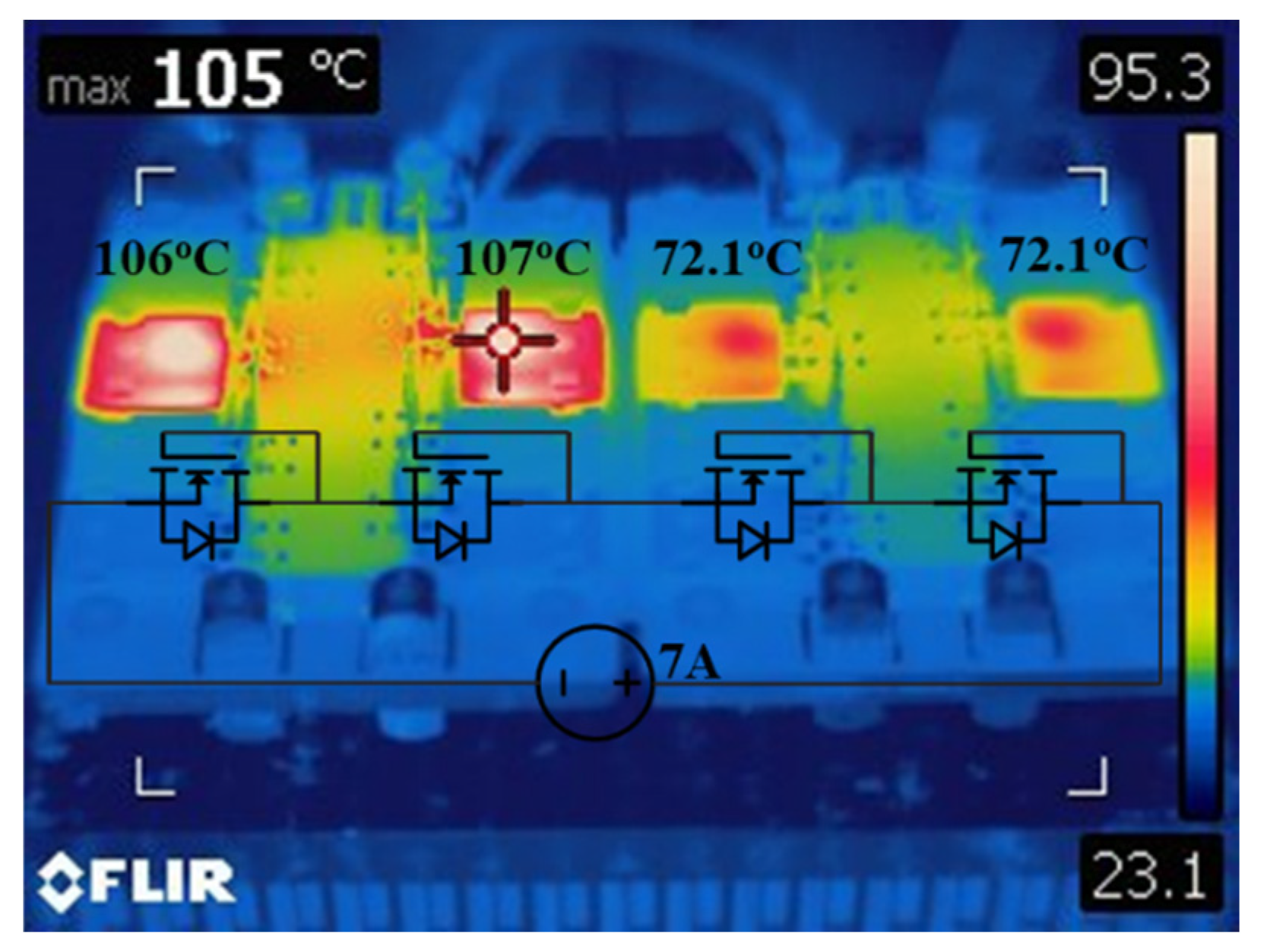
Figure 12, where four devices are connected in series and have different thermal resistance. The voltage drop on each device is around 5.2V when the drain and gate are shorted in forward conduction; the current is 7A when 36W loss is injected into the device. However, when it is in reverse conduction, the voltage drop is around 0.9V, which requires 5.8 times higher current to inject the same loss, bringing in higher current capacity requirements for both the power supply and the busbar.
3.2. Dynamic Thermal Impedance Extraction
It is also essential to extract thermal capacitance from the actual hardware, especially for junction temperature estimation when there is a load current surge. This test can utilize the temperature-sensitive electrical parameters (TSEP), such as the V
sd of the device. The V
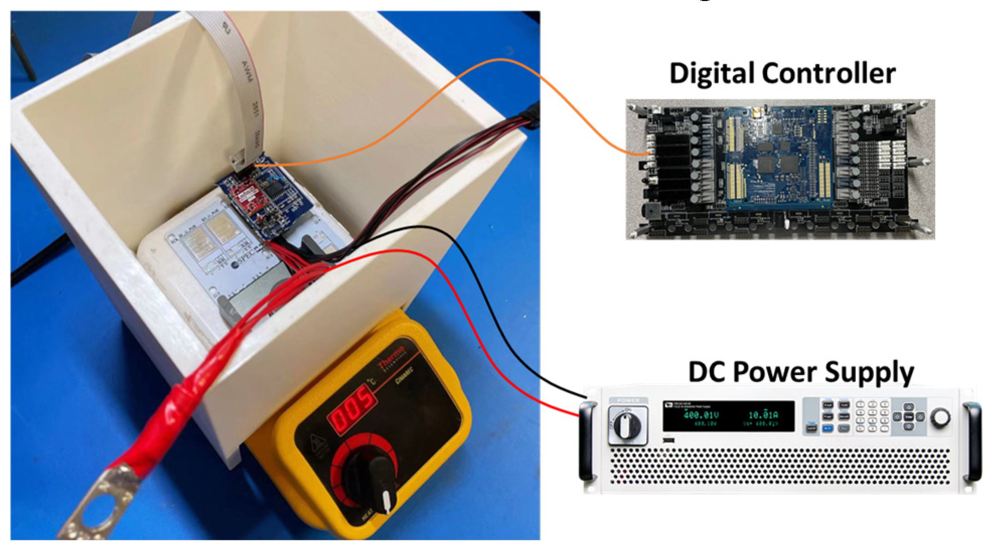
sd at a certain current can be correlated to the device’s junction temperature. The thermal capacitance can be extracted in the following steps as described in [C22]: first, correlation of the V
sd at 0.1A from 25
oC to 150
oC needs to be obtained using a thermal chamber or hot plate, as shown in
Figure 13; this can be done with a single device without attaching to the thermal management components, and the V
sd can be read by a digital controller or other voltage measurement methods. Typically, the V
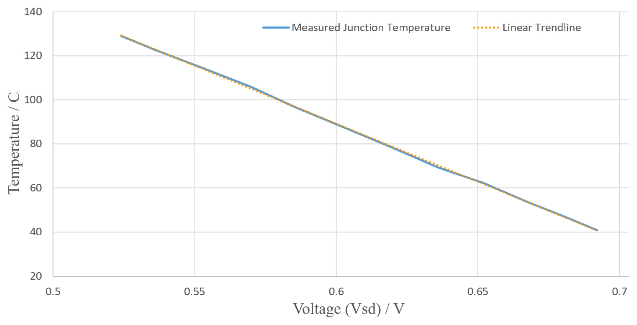
sd changes linearly with the temperature when the current is constant, as shown in
Figure 14.
After collecting the T-V
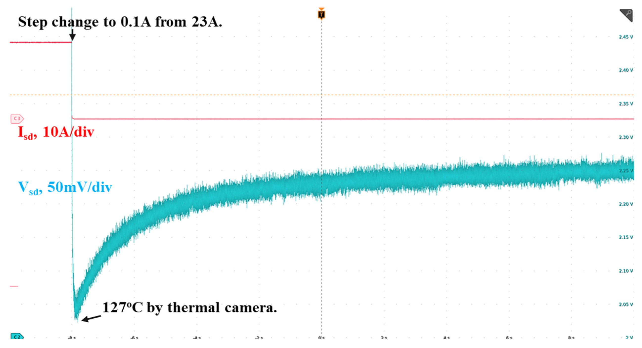
sd data, the MOSFET should be attached to its full thermal management system to extract its thermal impedance with the actual cooling condition. Heat the device to a higher temperature by reverse current conduction at a high current level, and then step down the power supply current to 0.1A quickly. Record the voltage V
sd change with the time. This represents the cooling down of the converter and each voltage point corresponding to a temperature vs. time data point. The thermal impedance can then be extracted by curve fitting to Equations (6) and (7) and extract the C
n and R
n in its Foster model in
Figure 10b. An example of a typical waveform for thermal impedance extraction is shown in
Figure 15. The device heats up in 23A reverse conduction; then step changes the current to 0.1A. The cooling curve is captured by an oscilloscope. Convert each voltage point to a temperature using the T-V
sd curve captured before.
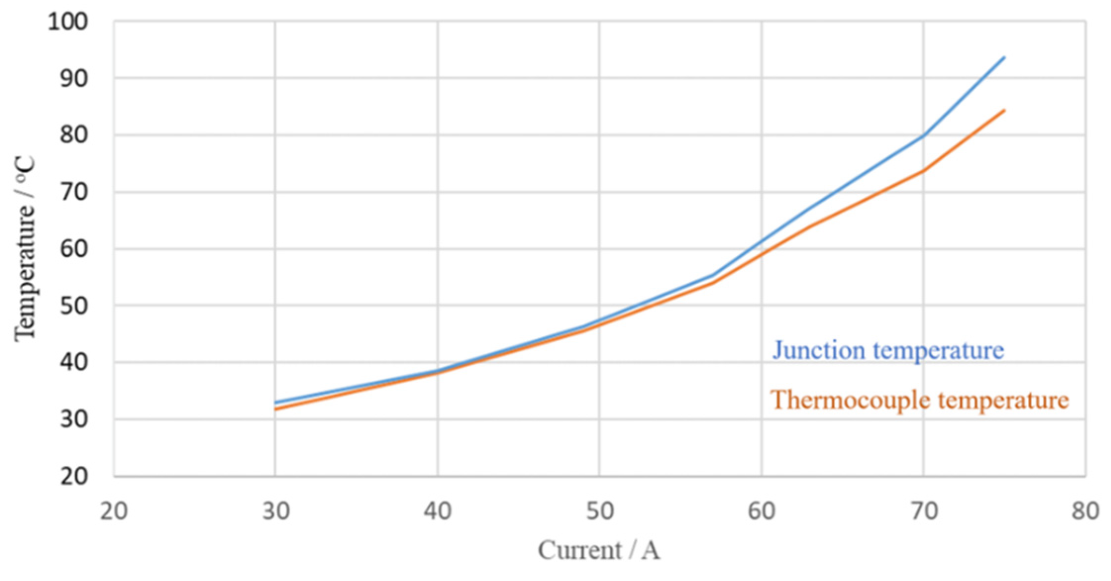
The dynamic thermal impedance extraction method can be extended to establish a correlation between the junction temperature and external temperature sensors located near the power semiconductors, such as built-in NTC thermistors, thermocouples, and thermal cameras used in the experiments. This correlation process mirrors the dynamic thermal impedance extraction approach. After obtaining the T-V
sd data, the devices are heated in reverse conduction to various temperatures, followed by step changes at each temperature level. This allows for plotting the temperature sensor versus junction temperature curve, as illustrated in
Figure 16.
4. Insulation Evaluation
4.1. DC Dielectric Withstand Test
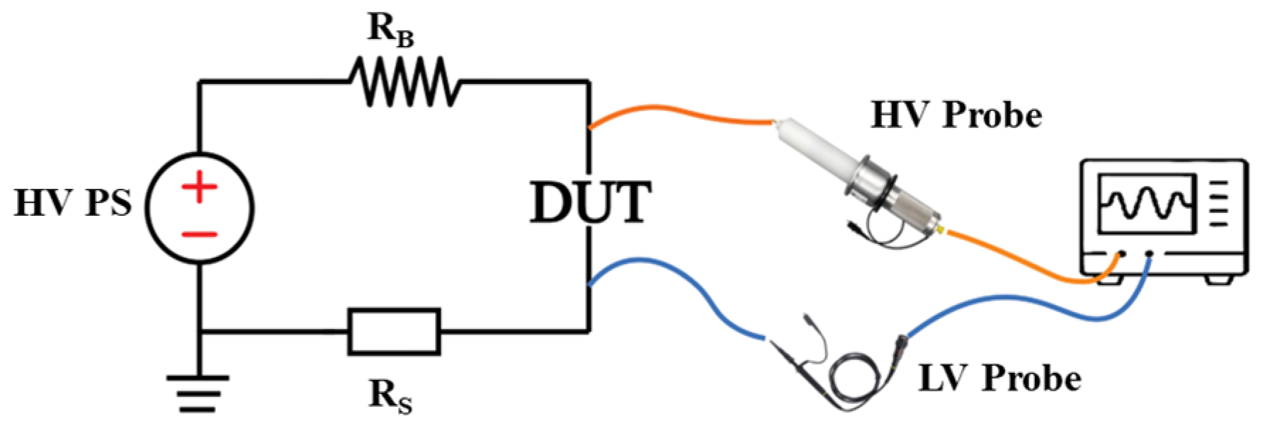
High-voltage converters must validate their insulation at both the component and system levels, including power semiconductor-to-heatsink insulation, busbar insulation, and transformer insulation. The dielectric withstand test, commonly known as the high potential (hi-pot) test, applies high voltage to assess insulation levels and must be conducted on all hardware to ensure safe operation before any high-voltage testing. While some commercial equipment is dedicated to the hi-pot test, it can also be quickly performed in the lab when a dedicated hi-pot machine is not available. A simplified approach involves using a high-voltage, low-current DC power supply with the Device Under Test (DUT) connected in series with a high-resistance blocking resistor (R
B) and a low-resistance sensing resistor (R
S) to observe the leakage current. An example of this dielectric withstand test for an Insulated Metal Substrate (IMS) of a SiC power module is shown in
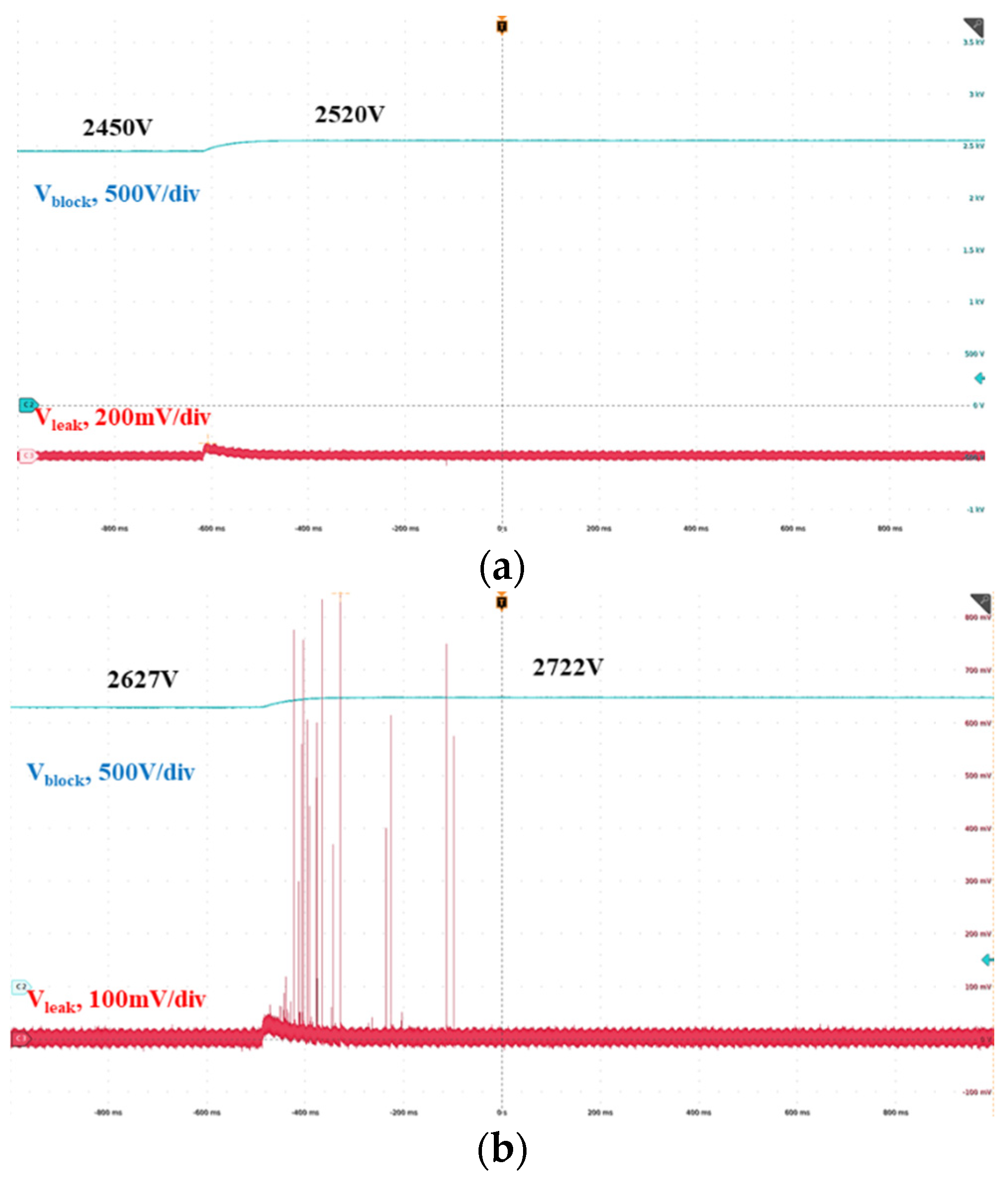
Figure 17, with the measurement results presented in
Figure 18. In the test setup, all copper plates on the single-layer IMS power module are connected to the same voltage potential, and the assembly is placed in series with the blocking resistor to the power supply. The power supply’s ground terminal is connected to the aluminum substrate of the IMS. The voltage is gradually increased in 100V increments, and the voltage across a 110kΩ sensing resistor is measured to extract the leakage current. The sample exhibits repetitive leakage current pulses as the voltage rises from 2627V to 2722V, with a dV/dt of approximately 1.2V/ms, indicating that the insulation capability is below 2.6kV. It remains adequate for a 1200V power module, typically operating at a bus voltage of 800V.
4.2. 60 Hz Sinusoidal Partial Discharge Measurement
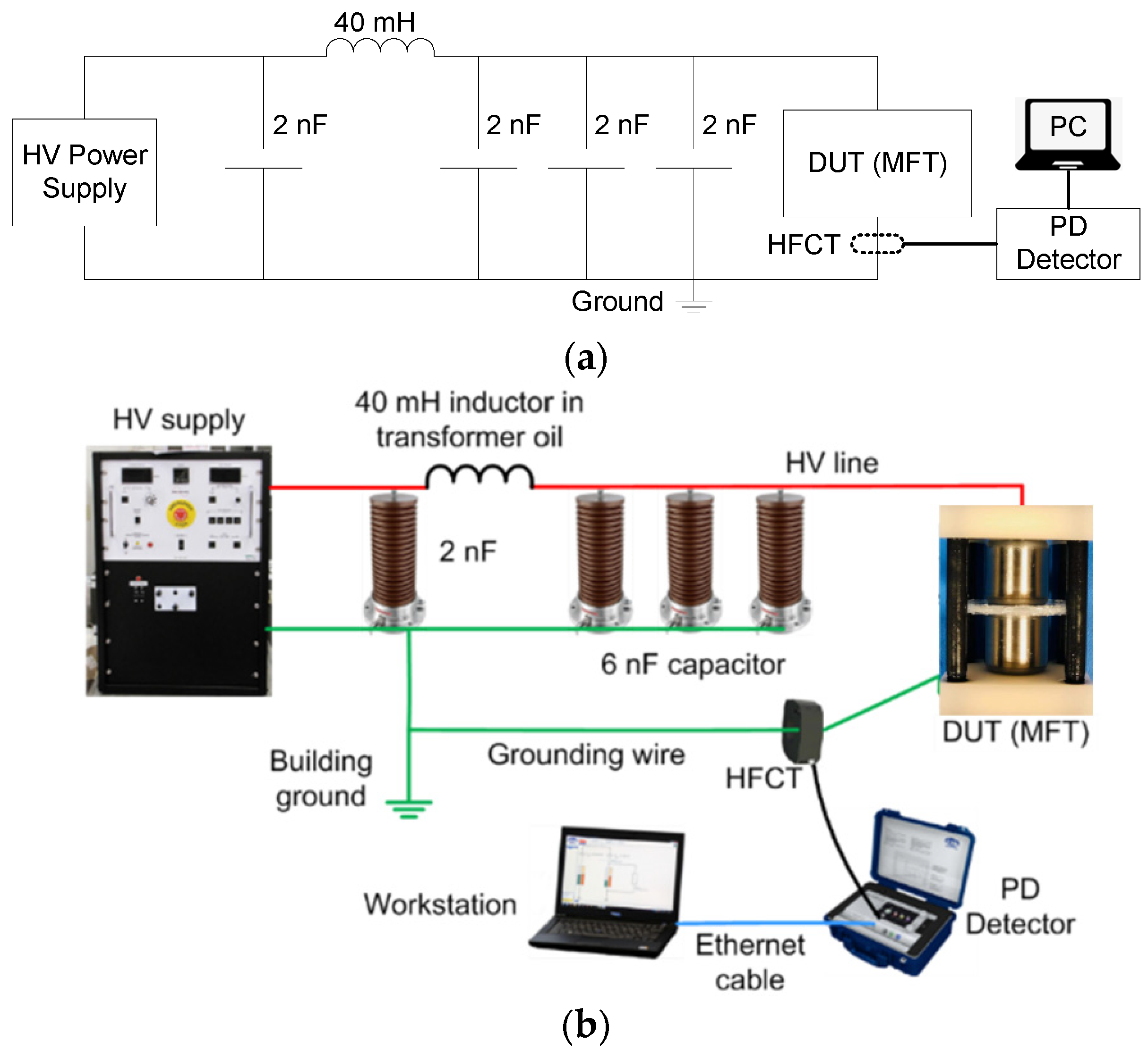
Partial Discharge (PD) is a phenomenon often occurring in insulation system defects (cavities), which can significantly affect lifetime and reliability. Many industry standards and regulations mandate PD tests for power electronics converters. Compliance with these standards is essential for ensuring the safety and reliability of electrical systems. The most common PD test is to measure under 60Hz sinusoidal waveform. An example circuit diagram of the 60Hz sinusoidal waveform PD test setup for a medium-frequency transformer (MFT) is shown in
Figure 19 [C25]. It includes a high-voltage power supply, a C-L-3C filter, a high-frequency current transformer (HFCT), and a PD detector. The PD measurement device’s frequency band is 100kHz to 500kHz, consistent with the IEC 60270 Standard. The cable terminals and the high-voltage inductor are placed in transformer oil baths to minimize PD from cable termination and inductor terminals. The discharge pulses sensed by the HFCT are recorded and processed by the PD detector (Doble PD Smart) and transferred to a computer for monitoring and visualization. As all interconnections are appropriately terminated, this setup can conduct both AC and DC PD tests up to 30kV with a background noise level of 5pC.
Figure 20 shows the PD test process under a 60 Hz sinusoidal waveform. The orange curve represents the applied voltage RMS value, and the blue curve is the PD charge magnitude. Continued PD happens when the voltage reaches 2.7kV RMS.
Figure 21 shows the PD pattern diagram under AC 60Hz peak-to-peak 7.6kV voltage. It is a typical internal PD pattern with a maximum charge of around 400pC.
4.3. High-Frequency PWM Partial Discharge Measurement
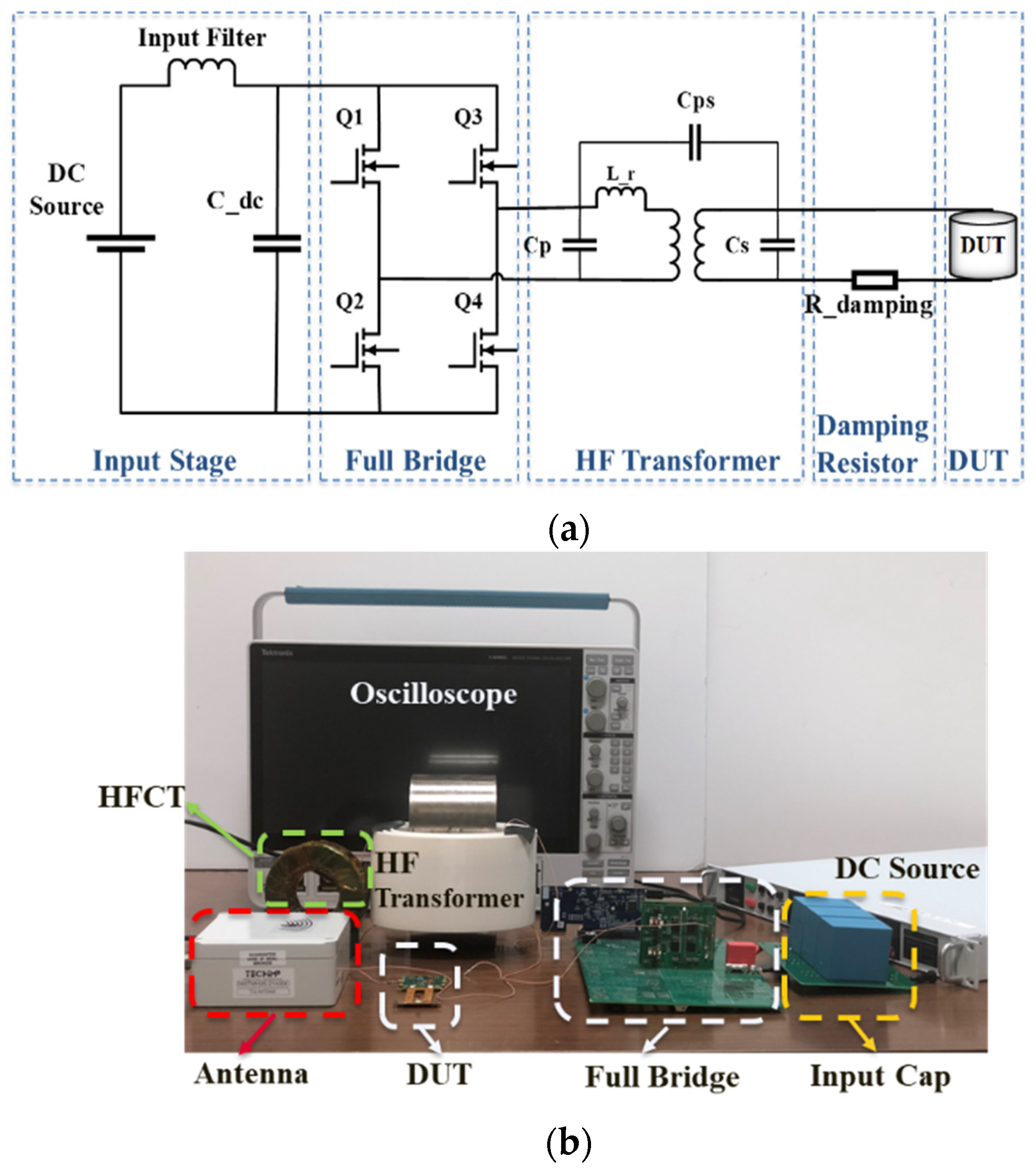
With the development of wide bandgap power devices, higher voltage, and high-frequency square wave voltages are applied in power electronics systems, challenging lifetime and reliability. There is a high demand to characterize the PD under high-frequency PWM voltage stress with fast switching speed and high dV/dt. A high-voltage, PWM waveform PD test platform is illustrated in
Figure 22 [C26]. It consists of a GaN-based full-bridge converter with a DC voltage source, a step-up transformer, a variable damping resistor, and the DUT. The full-bridge inverter generates a low-voltage PWM wave, then step up by the step-up transformer. A variable damping resistor controls the output voltage dV/dt and quality factor. The GaN-based full-bridge inverter is realized using 600V GaN FET (TI LMG3410R050) and controlled by a Digital Signal Processor (DSP). The step-up transformer is designed with amorphous magnetic cores with a turns-ratio of 1:12.5; 3D printed Acrylonitrile Butadiene Styrene (ABS) bobbins are used to construct the winding structure. A high-bandwidth HFCT (Pearson 6585) and an antenna (Techimp TEM antenna) are used for PD signal detection. The TEM antenna and HFCT have bandwidths of 100MHz-3GHz and 400Hz-250MHz, respectively. The setup was tested at higher than ±5kV to verify the background noise level (able to affect the sensitivity of PD detection).
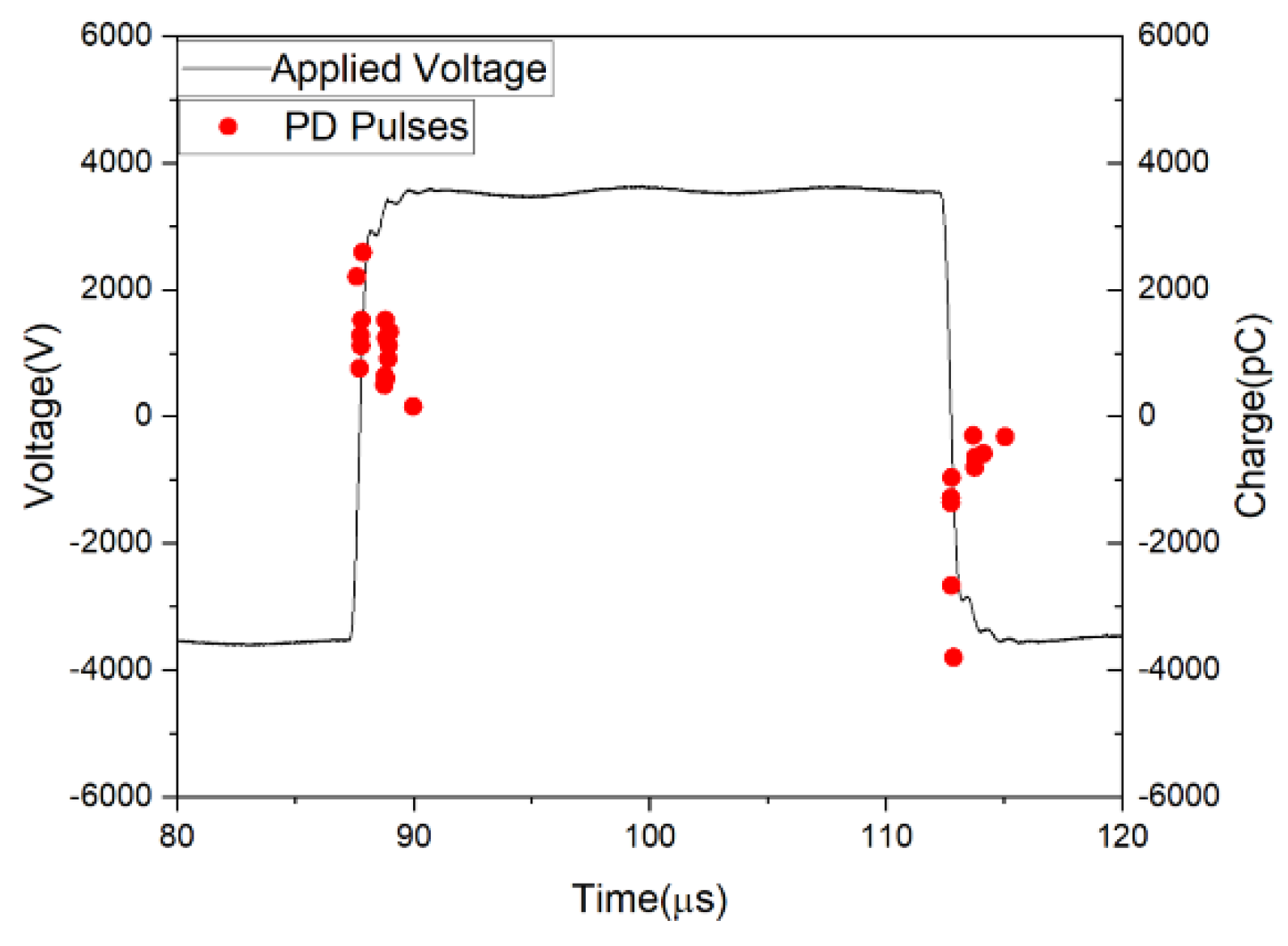
Figure 23 shows the test waveforms under 20kHz and up to 7kV peak-to-peak PWM pulses for a DUT. Based on the experimental data, the PD pattern diagram is plotted. The red dots represent PD pulses, which are located at the rising and falling edges of the PWM waveform.
5. Full Power Validation
The WBG high-power converters must be tested under their full voltage, current, and thermal stress. Ideally, it can be quickly done by connecting it to a resistive load. However, this will require a high-power supply and high power load bank with cooling capability. In many labs this is not feasible. In some cases, the facility’s electric grid capacity is also an issue. The resistive load test also causes environmental hazards (heating the space) and wastes lots of energy, so it should be avoided. Testing the converter with circulating power or regenerative is an attractive solution.
5.1. Circulating Test for Three-Phase Inverter
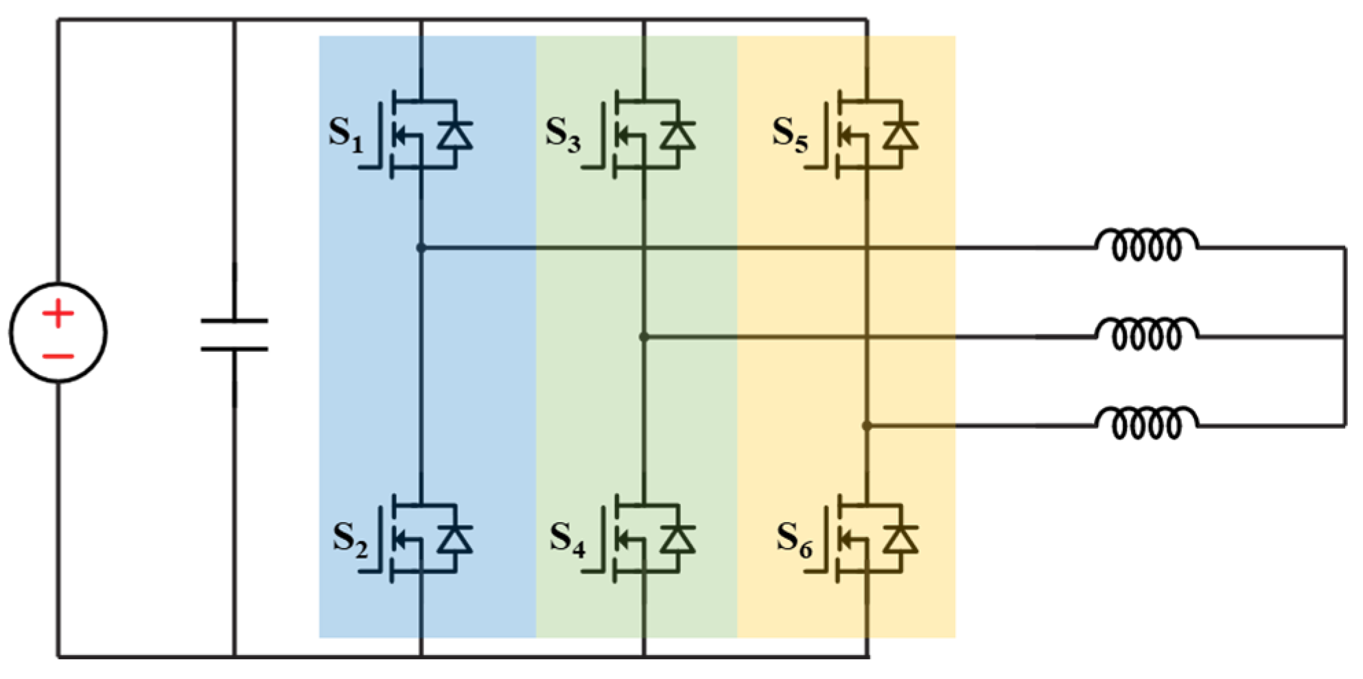
A three-phase converter/inverter can be configured and tested with inductive load. In this case, the DC power supply only provides the losses (
Figure 24). The low frequency (60Hz) inverter output voltage is applied to the inductor; hence, this test will require three high current and high inductance-value inductors. These kinds of inductors may not be available in most labs. For example, testing a 480V/75kVA three-phase inverter to its full power condition requires an above 8mH inductor, which will be huge and heavy. Since the power factor is zero in this test, the tested efficiency and thermal performance also differ from the actual case when the power factor is high.
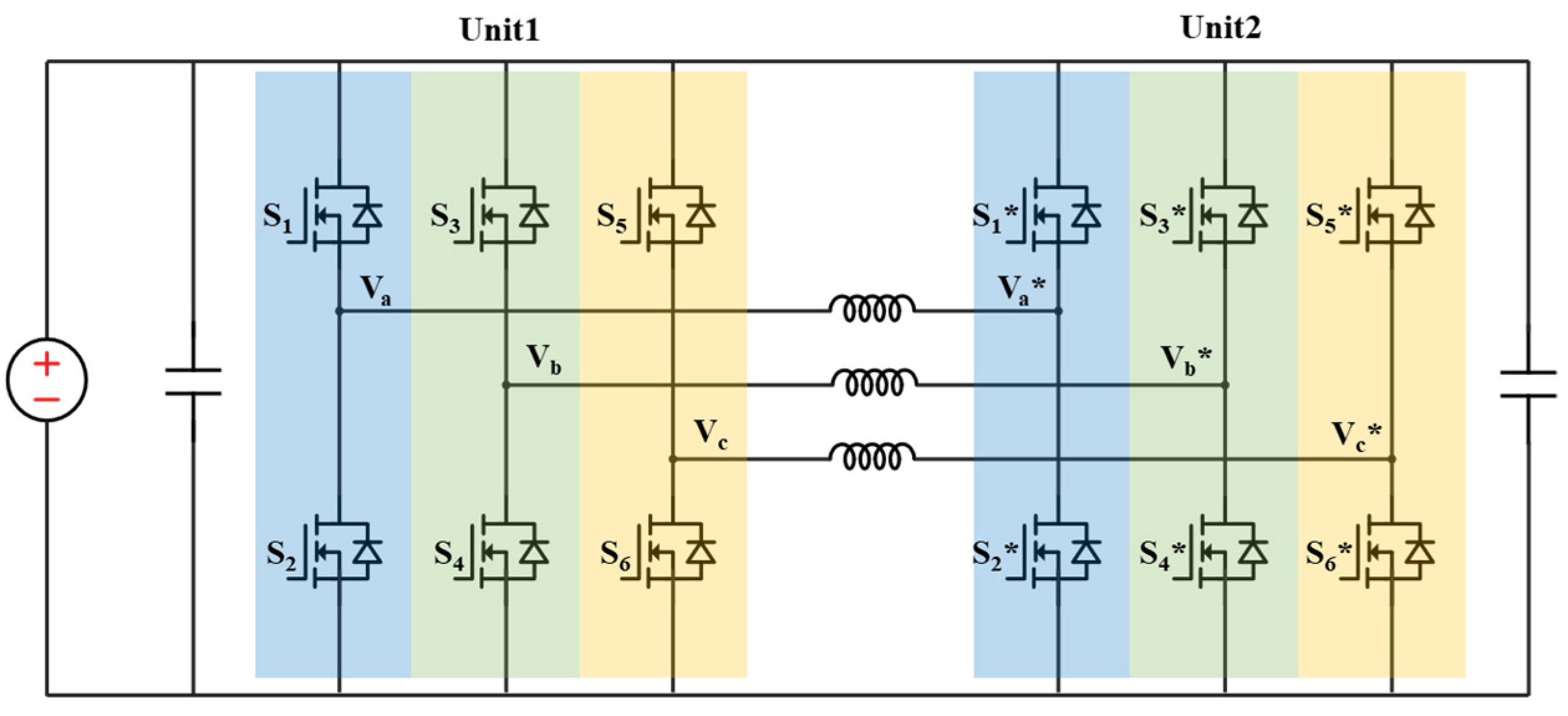
Another way to achieve a full-power test is to circulate the power between converters (also called back-to-back test or pump-back test) for a single-phase inverter [C27-C28] or between two three-phase inverters [C29-C31], as shown in
Figure 25. In this case, the voltage applied to the inductor is the difference between two inverter output voltages. So, a much smaller inductance can be used.
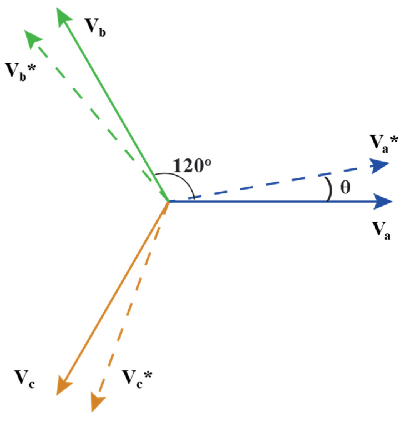
The test can be done using open-loop or closed-loop control. The current can be adjusted by changing the phase shift (θ in
Figure 26) between the two legs on the same inductor while maintaining a fixed modulation index. Efficiency can be measured accurately since the DC supply provides only the losses; hence, each converter’s losses can be estimated to be half of the DC supply power.
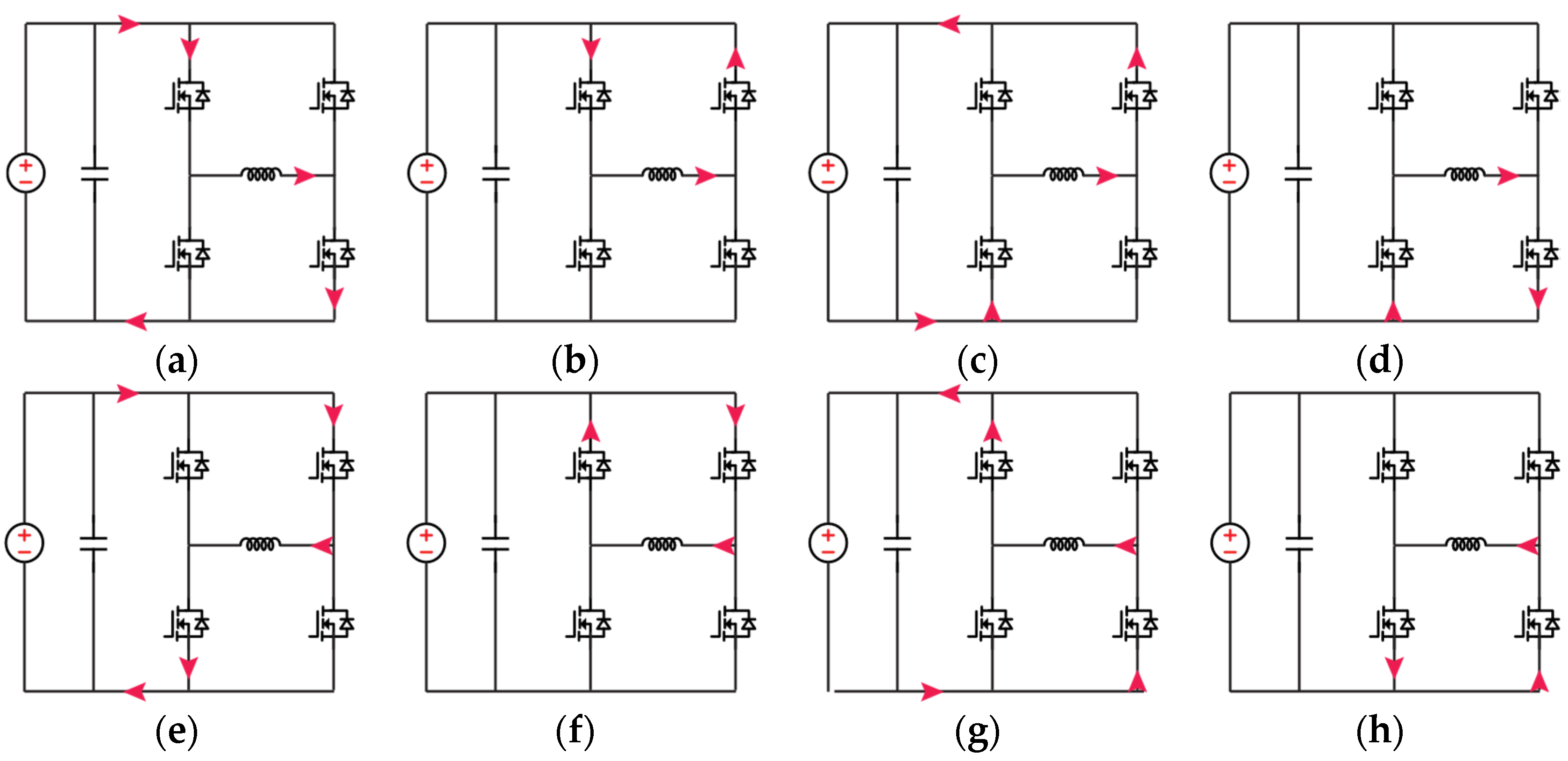
The requirement for power supply is much lower since the WBG power converter usually has higher than 98% efficiency. Testing two 100kVA inverters only requires a power supply of less than 4kW. The inductor losses are included in this estimation and can be subtracted if the inductor loss can be estimated separately. High DC link capacitance should be in place for the single-phase test due to the low-frequency AC component. In six-phase legs tests, the two inverters operate as three switching cells, so there is a 120-degree phase difference between three units, and the DC voltage ripple is canceled out more by the balanced three-phase current. Eight states for each switching cell are presented in
Figure 27, while
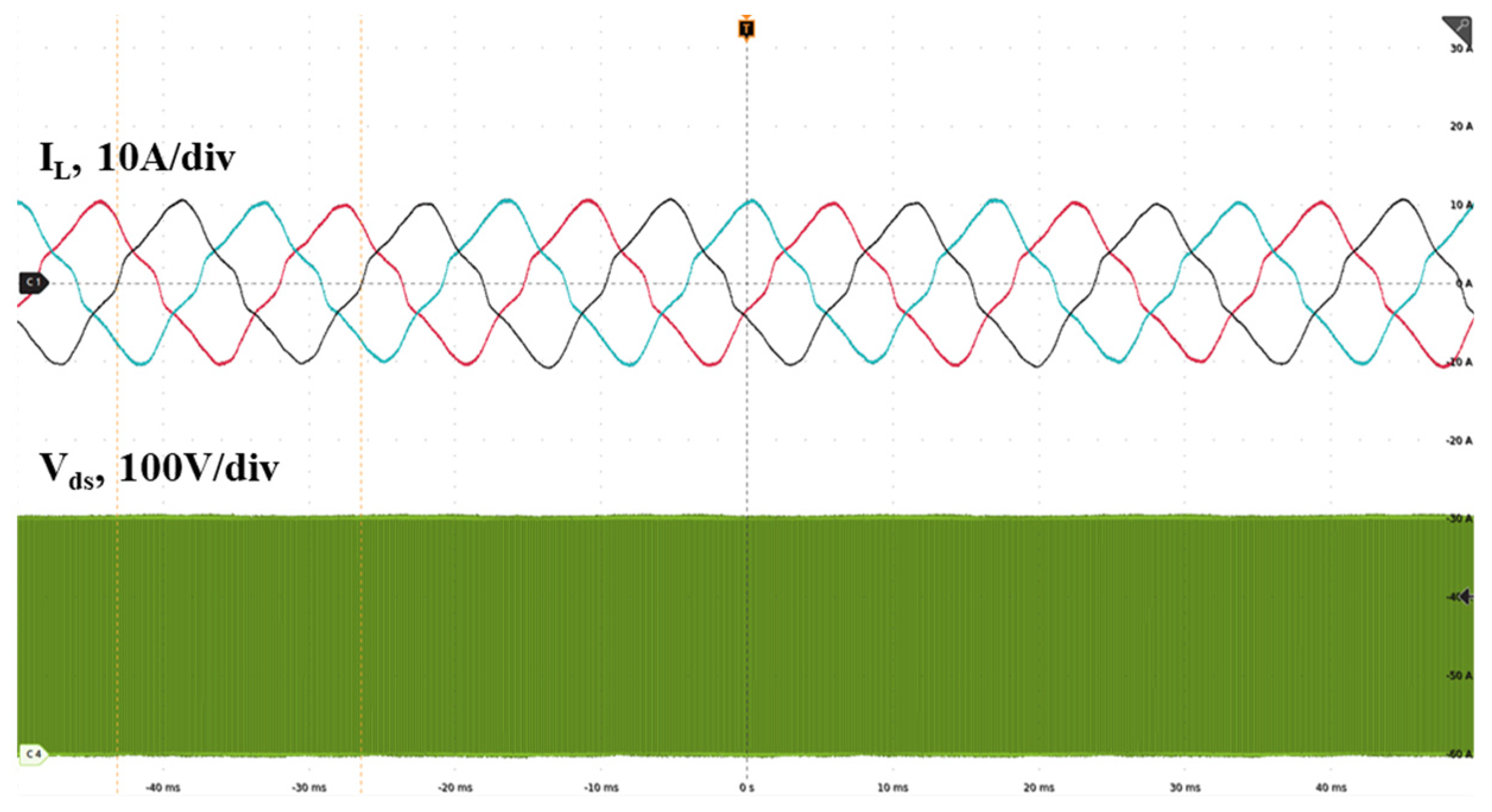
Figure 28 presents typical open-loop experimental waveforms.
5.2. Circulating Test for Isolated Converter
Many high-voltage and high-power converters, such as the Solid-State Transformers (SST), often employ a modular configuration [C2-C3, C32] using many identical cells or submodules. Each submodule needs to be pre-validated before any system-level integration. A pump-back circulating power test can be utilized to validate isolated submodules with a 1:1 conversion ratio, such as a DAB or a CLLC. In this case, both the power electronics power stage and the magnetics are evaluated under the desired operation condition. [C33] presents an example test of a 200kW SiC submodule in a Dual Active Bridge (DAB) converter and CLLC resonant converter using the configuration shown in
Figure 29a. The tested converter demonstrated 99.6% at 200 kW, hence the DC power supply only needs to provide very little power during the test. Testing AC-AC SST submodules is discussed in detail in [C34-C35], using a circuit like
Figure 29b.
6. Conclusions
This paper fills a critical knowledge gap in hardware testing methodology for the emerging WBG-based high-power converters. The proposed testing methodology is essential for new hardware development and validation, offering a comprehensive framework for assessing various aspects of a high-power converter, including switching characteristics, driving circuit functionality, thermal management performance, insulation levels, and continuous operation at full power capacity.
The double pulse test (DPT) is an important platform for power semiconductor device switching performance and switching loss characterizations, Coss and Qoss measurement, optimization of gate driving circuits, assess magnetics components, validation of overcurrent protection mechanisms, and measurement device on-resistance. Heat loss injection and accurate temperature sensing, which are essential for extracting key thermal parameters with actual cooling conditions for high-power converters are also discussed in detail. A correlation method between temperature sensor measurements and junction temperature is presented to enhance the accuracy of device temperature monitoring during converter operation.
Dielectric withstand tests are introduced to ensure converter reliability and safety, verifying insulation at both component and system levels. This verification extends to partial discharge measurements under conventional 60 Hz sinusoidal stress and high-frequency square wave voltage stress. The significance of testing converters under full voltage, current, and thermal conditions is discussed with a focus on the power circulating test for both isolated and non-isolated converters, which minimizes the electricity consumption and equipment requirement, underscoring the practical effectiveness and applicability of the proposed testing methodologies.
References
- J. Millán, P. Godignon, X. Perpiñà, A. Pérez-Tomás and J. Rebollo, “A Survey of Wide Bandgap Power Semiconductor Devices,” in IEEE Transactions on Power Electronics, vol. 29, no. 5, pp. 2155-2163, May 2014. [CrossRef]
- A. Q. Huang, “Wide bandgap (WBG) power devices and their impacts on power delivery systems,” 2016 IEEE International Electron Devices Meeting (IEDM), San Francisco, CA, USA, 2016, pp. 20.1.1-20.1.4. [CrossRef]
- Z. Chen and A. Q. Huang, “Extreme high efficiency enabled by silicon carbide (SiC) power devices,” Materials Science in Semiconductor Processing, Volume 172, 2024, 108052, ISSN 1369-8001. [CrossRef]
- S. Sen, “ Medium Voltage Extreme Fast Charger based on Novel Medium Voltage SiC Power Devices,” Ph.D. dissertation, Department of Electrical and Computer Engineering, the University of Texas at Austin, Austin, TX, USA, 2021.
- Z. Chen, H. S. Rizi, W. Xu, R. Yu and A. Q. Huang, “Hardware Design of a 150kW/1500V All-SiC Grid-forming Photovoltaic Synchronous Generator (PVSG),” 2022 IEEE Applied Power Electronics Conference and Exposition (APEC), Houston, TX, USA, 2022, pp. 1977-1984.
- Z. Chen, C. Chen, H. S. Rizi and A. Q. Huang, “A High Power Density 75kVA Air-Cooled SiC Intelligent Power Stage (IPS) As A Universal Building Block for Grid Applications,” 2023 IEEE Applied Power Electronics Conference and Exposition (APEC), Orlando, FL, USA, 2023, pp. 2299-2306.
- Z. Chen, D. Boroyevich, P. Mattavelli and K. Ngo, “A frequency-domain study on the effect of DC-link decoupling capacitors,” 2013 IEEE Energy Conversion Congress and Exposition, Denver, CO, USA, 2013, pp. 1886-1893. [CrossRef]
- Z. Zhang, B. Guo, F. F. Wang, E. A. Jones, L. M. Tolbert and B. J. Blalock, “Methodology for Wide Band-Gap Device Dynamic Characterization,” in IEEE Transactions on Power Electronics, vol. 32, no. 12, pp. 9307-9318, Dec. 2017. [CrossRef]
- W. Zhang, Z. Zhang and F. Wang, “Review and Bandwidth Measurement of Coaxial Shunt Resistors for Wide-Bandgap Devices Dynamic Characterization,” 2019 IEEE Energy Conversion Congress and Exposition (ECCE), Baltimore, MD, USA, 2019, pp. 3259-3264. [CrossRef]
- W. Zhang, Z. Zhang, F. Wang, E. V. Brush and N. Forcier, “High-Bandwidth Low-Inductance Current Shunt for Wide-Bandgap Devices Dynamic Characterization,” in IEEE Transactions on Power Electronics, vol. 36, no. 4, pp. 4522-4531, April 2021. [CrossRef]
- K. Wang, X. Yang, H. Li, L. Wang and P. Jain, “A High-Bandwidth Integrated Current Measurement for Detecting Switching Current of Fast GaN Devices,” in IEEE Transactions on Power Electronics, vol. 33, no. 7, pp. 6199-6210, July 2018. [CrossRef]
- W. Zhang, S. B. Sohid, F. Wang, H. Cui and B. Holzinger, “High-Bandwidth Combinational Rogowski Coil for SiC MOSFET Power Module,” in IEEE Transactions on Power Electronics, vol. 37, no. 4, pp. 4397-4405, April 2022. [CrossRef]
- E. A. Jones et al., “Characterization of an enhancement-mode 650-V GaN HFET,” 2015 IEEE Energy Conversion Congress and Exposition (ECCE), Montreal, QC, Canada, 2015, pp. 400-407. [CrossRef]
- T. Liu, Y. Feng, R. Ning, W. Wang, T. T. Y. Wong and Z. J. Shen, “Extraction of parasitic inductances of SiC MOSFET power modules based on two-port S-parameters measurement,” 2017 IEEE Energy Conversion Congress and Exposition (ECCE), Cincinnati, OH, USA, 2017, pp. 5475-5482. [CrossRef]
- J. Chen et al., “A Novel Power Loop Parasitic Extraction Approach for Paralleled Discrete SiC MOSFETs on Multilayer PCB,” in IEEE Journal of Emerging and Selected Topics in Power Electronics, vol. 9, no. 5, pp. 6370-6384, Oct. 2021. [CrossRef]
- B. T. DeBoi, A. N. Lemmon, B. W. Nelson, C. D. New and D. M. Hudson, “Improved Methodology for Parasitic Characterization of High-Performance Power Modules,” in IEEE Transactions on Power Electronics, vol. 35, no. 12, pp. 13400-13408, Dec. 2020. [CrossRef]
- Y. S. Cao et al., “Inductance Extraction for PCB Prelayout Power Integrity Using PMSR Method,” in IEEE Transactions on Electromagnetic Compatibility, vol. 59, no. 4, pp. 1339-1346, Aug. 2017. [CrossRef]
- H. Gui et al., “Modeling and Mitigation of Multiloops Related Device Overvoltage in Three-Level Active Neutral Point Clamped Converter,” in IEEE Transactions on Power Electronics, vol. 35, no. 8, pp. 7947-7959, Aug. 2020. [CrossRef]
- H. Gui et al., “Development of High-Power High Switching Frequency Cryogenically Cooled Inverter for Aircraft Applications,” in IEEE Transactions on Power Electronics, vol. 35, no. 6, pp. 5670-5682, June 2020. [CrossRef]
- Z. Chen and A. Q. Huang, “High Performance SiC Power Module Based on Repackaging of Discrete SiC Devices,” in IEEE Transactions on Power Electronics, vol. 38, no. 8, pp. 9306-9310, Aug. 2023. [CrossRef]
- Z. Ni, X. Lyu, O. P. Yadav, B. N. Singh, S. Zheng and D. Cao, “Overview of Real-Time Lifetime Prediction and Extension for SiC Power Converters,” in IEEE Transactions on Power Electronics, vol. 35, no. 8, pp. 7765-7794, Aug. 2020. [CrossRef]
- Z. Chen, C. Chen and A. Q. Huang, “Driver Integrated Online Rds-on Monitoring Method for SiC Power Converters,” 2022 IEEE Energy Conversion Congress and Exposition (ECCE), Detroit, MI, USA, 2022, pp. 01-07. [CrossRef]
- A. S. Bahman, K. Ma and F. Blaabjerg, “Thermal impedance model of high power IGBT modules considering heat coupling effects,” 2014 International Power Electronics and Application Conference and Exposition, Shanghai, China, 2014, pp. 1382-1387. [CrossRef]
- Infineon, “Transient Thermal Measurements and Thermal Equivalent Circuit Models,” Appl. Note AN2015-10 V 1.2, 2020.
- Z. Guo and A. Q. Huang, “Characterizations of Partial Discharge in Modern Power Electronics,” in IEEE Journal of Emerging and Selected Topics in Power Electronics. [CrossRef]
- Z. Guo, H. Li, P. Cheetham and N. Guvvala, “Partial Discharge Characterization of Solid-Dielectric-Based Transformer Under High Frequency High dv/dt PWM Voltage for MV Applications,” 2023 IEEE Applied Power Electronics Conference and Exposition (APEC), Orlando, FL, USA, 2023, pp. 301-305. [CrossRef]
- S. Mocevic et al., “Power Cell Design and Assessment Methodology Based on a High-Current 10-kV SiC MOSFET Half-Bridge Module,” in IEEE Journal of Emerging and Selected Topics in Power Electronics, vol. 9, no. 4, pp. 3916-3935, Aug. 2021. [CrossRef]
- X. Lin, L. Ravi, R. Burgos and D. Dong, “Hybrid Voltage Balancing Approach for Series-Connected SiC MOSFETs for DC–AC Medium-Voltage Power Conversion Applications,” in IEEE Transactions on Power Electronics, vol. 37, no. 7, pp. 8104-8117, July 2022. [CrossRef]
- U. -M. Choi, S. Jørgensen and F. Blaabjerg, “Advanced Accelerated Power Cycling Test for Reliability Investigation of Power Device Modules,” in IEEE Transactions on Power Electronics, vol. 31, no. 12, pp. 8371-8386, Dec. 2016. [CrossRef]
- X. She, T. Frangieh and R. Datta, “On the Switching Frequency of Hysteresis Control in a Silicon Carbide Converter Pump-Back Test,” in IEEE Transactions on Industry Applications, vol. 54, no. 5, pp. 4886-4893, Sept.-Oct. 2018. [CrossRef]
- S. Pu, F. Yang, B. T. Vankayalapati and B. Akin, “Aging Mechanisms and Accelerated Lifetime Tests for SiC MOSFETs: An Overview,” in IEEE Journal of Emerging and Selected Topics in Power Electronics, vol. 10, no. 1, pp. 1232-1254, Feb. 2022. [CrossRef]
- X. She, A. Q. Huang and R. Burgos, “Review of Solid-State Transformer Technologies and Their Application in Power Distribution Systems,” in IEEE Journal of Emerging and Selected Topics in Power Electronics, vol. 1, no. 3, pp. 186-198, Sept. 2013. [CrossRef]
- W. Xu, Z. Guo, A. Vetrivelan, R. Yu and A. Q. Huang, “Hardware Design of a 13.8-kV/3-MVA PV Plus Storage Solid-State Transformer (PVS-SST),” in IEEE Journal of Emerging and Selected Topics in Power Electronics, vol. 10, no. 4, pp. 3571-3586, Aug. 2022.
- D. Dong, M. Agamy, J. Z. Bebic, Q. Chen and G. Mandrusiak, “A Modular SiC High-Frequency Solid-State Transformer for Medium-Voltage Applications: Design, Implementation, and Testing,” in IEEE Journal of Emerging and Selected Topics in Power Electronics, vol. 7, no. 2, pp. 768-778, June 2019. [CrossRef]
- A Modular SiC High-Frequency Solid-State Transformer for Medium-Voltage Applications: Design, Implementation, and Testing,” in IEEE Journal of Emerging and Selected Topics in Power Electronics, vol. 7, no. 2, pp. 768-778, June 2019. [CrossRef]
Figure 1.
Examples of Power Electronics Power Stages (PEPSs). (a) 1200V/4.3mΩ SiC six-phase power stage. (b) 2400V/7mΩ SiC full-bridge power stage. (c) 1200V/7.3mΩ SiC full-bridge plus IGBT full-bridge power stage. (d) 900V/2.5mΩ three level power stage.
Figure 1.
Examples of Power Electronics Power Stages (PEPSs). (a) 1200V/4.3mΩ SiC six-phase power stage. (b) 2400V/7mΩ SiC full-bridge power stage. (c) 1200V/7.3mΩ SiC full-bridge plus IGBT full-bridge power stage. (d) 900V/2.5mΩ three level power stage.
Figure 2.
Summary of the design evaluation test.
Figure 2.
Summary of the design evaluation test.
Figure 3.
Test setup for double pulse test (DPT). (a) Bottom side DPT. (b) Top side DPT.
Figure 3.
Test setup for double pulse test (DPT). (a) Bottom side DPT. (b) Top side DPT.
Figure 4.
Typical waveform for double pulse test.
Figure 4.
Typical waveform for double pulse test.
Figure 7.
A gate driver integrated online voltage measurement and over-current protection circuit.
Figure 7.
A gate driver integrated online voltage measurement and over-current protection circuit.
Figure 8.
Over current protection validation in double pulse test.
Figure 8.
Over current protection validation in double pulse test.
Figure 9.
On-resistance extraction in double pulse test.
Figure 9.
On-resistance extraction in double pulse test.
Figure 10.
Thermal network equivalent circuit models. (a) Cauer model. (b) Foster model.
Figure 10.
Thermal network equivalent circuit models. (a) Cauer model. (b) Foster model.
Figure 11.
Loss injection for thermal management evaluation of a six-phase power stage. (a) Reverse conduction for loss injection. (b) Forward conduction for loss injection.
Figure 11.
Loss injection for thermal management evaluation of a six-phase power stage. (a) Reverse conduction for loss injection. (b) Forward conduction for loss injection.
Figure 12.
Thermal camera image in a forward conduction loss heat injection test.
Figure 12.
Thermal camera image in a forward conduction loss heat injection test.
Figure 13.
Example for temperature calibration.
Figure 13.
Example for temperature calibration.
Figure 14.
Vsd measurement at varies Tj.
Figure 14.
Vsd measurement at varies Tj.
Figure 15.
A typical waveform for thermal impedance extraction.
Figure 15.
A typical waveform for thermal impedance extraction.
Figure 16.
Correlation curve between thermocouple and junction temperature.
Figure 16.
Correlation curve between thermocouple and junction temperature.
Figure 17.
Test setup for DC dielectric withstand test.
Figure 17.
Test setup for DC dielectric withstand test.
Figure 18.
Dielectric withstand test result. (a) Voltage increases from 2450V to 2520V. (b) Voltage increases from 2627V to 2722V.
Figure 18.
Dielectric withstand test result. (a) Voltage increases from 2450V to 2520V. (b) Voltage increases from 2627V to 2722V.
Figure 19.
Circuit diagram of a 60 Hz sinusoidal waveform PD test platform. (a) Circuit diagram. (b) Hardware setup.
Figure 19.
Circuit diagram of a 60 Hz sinusoidal waveform PD test platform. (a) Circuit diagram. (b) Hardware setup.
Figure 20.
PD test at 60Hz sinusoidal waveform (applied voltage and PD charge).
Figure 20.
PD test at 60Hz sinusoidal waveform (applied voltage and PD charge).
Figure 21.
PD pattern diagram at AC 60 Hz peak-to-peak 7.6 kV.
Figure 21.
PD pattern diagram at AC 60 Hz peak-to-peak 7.6 kV.
Figure 22.
A high-frequency high-voltage PWM waveform PD test platform. (a) Circuit diagram. (b) Hardware setup.
Figure 22.
A high-frequency high-voltage PWM waveform PD test platform. (a) Circuit diagram. (b) Hardware setup.
Figure 23.
PD pattern diagram under 20 kHz 7 kV peak-to-peak PWM waveform.
Figure 23.
PD pattern diagram under 20 kHz 7 kV peak-to-peak PWM waveform.
Figure 24.
Inductive load three phases circulating test.
Figure 24.
Inductive load three phases circulating test.
Figure 25.
Configuration of the six-phase legs pump-back circulating test.
Figure 25.
Configuration of the six-phase legs pump-back circulating test.
Figure 26.
Phasor diagram for pump-back circulating test.
Figure 26.
Phasor diagram for pump-back circulating test.
Figure 27.
Switching states in the pump-back circulating test.
Figure 27.
Switching states in the pump-back circulating test.
Figure 28.
Typical experimental waveform for circulating test.
Figure 28.
Typical experimental waveform for circulating test.
Figure 29.
Pump-back circulating test for the isolated converter. (a) Pump-back test for isolated DC-DC converter. (b) Pump-back test for isolated AC-AC converter.
Figure 29.
Pump-back circulating test for the isolated converter. (a) Pump-back test for isolated DC-DC converter. (b) Pump-back test for isolated AC-AC converter.
|
Disclaimer/Publisher’s Note: The statements, opinions and data contained in all publications are solely those of the individual author(s) and contributor(s) and not of MDPI and/or the editor(s). MDPI and/or the editor(s) disclaim responsibility for any injury to people or property resulting from any ideas, methods, instructions or products referred to in the content. |
© 2024 by the authors. Licensee MDPI, Basel, Switzerland. This article is an open access article distributed under the terms and conditions of the Creative Commons Attribution (CC BY) license (http://creativecommons.org/licenses/by/4.0/).
