
Submitted:
20 September 2024
Posted:
24 September 2024
You are already at the latest version
Abstract
Waveform generation as part of an on-chip built-in self-test (BIST) circuitry often necessitates sufficient linearity without expensive hardware overhead. Achieving high linearity is critical for accurate signal generation, especially in applications requiring high precision, such as biomedical and instrumentation. Currently, achieving the high linearity and precision required in signal generators often relies on costly hardware such as automated test equipment (ATE). This paper presents a DAC based hardware synthesizable arbitrary waveform generator. We use a low-cost DAC and a fully digital on-chip testing and calibration approach to nullify the effect of the DAC’s non-linearity on the generated waveform. The ultra-low cost and high linearity benefit of the proposed waveform generator makes it highly suitable for integration into resource-constrained systems. The proposed approach is validated using simulation results of the small-area DAC designed in TSMC 0.18um technology and the testing and calibration algorithms implemented in MATLAB. The DAC, designed with a matching accuracy at only the 5-bit level, is able to generate a signal with an ENOB of 12 bits alongside a SFDR and THD surpassing 100 dB. This high level of signal purity is consistently maintained across 100 Monte-Carlo simulations, demonstrating the robustness of the architecture against PVT variations as well as random mismatches.
Keywords:
waveform generation
; BIST
; ATE
; DAC
; low-cost
; hardware synthesizable
; on-chip
1. Introduction
Post-manufacturing testing and characterization of analog/mixed signal (AMS) circuits have become increasingly important in the electronic industry recently due to their wide range of applications [1]. Recently, in safety-critical applications like automotive and medicine, where in-field failures can be catastrophic, there has been a notable rise in the utilization of Integrated circuits (ICs). One common way to improve the reliability of AMS circuits is through parametric testing. However, AMS circuit testing is time-consuming and expensive. Also, as AMS circuits migrate to newer technologies, their performance improves significantly; hence testing becomes more and more expensive. In fact, test costs dominate the total cost of SoCs. [2,3].
The standard post-production test involves high-precision instruments, such as automatic test equipment [4], which can be quite expensive. Designing or implementing a high-purity test stimulus has proven to be either complex or cost-prohibitive. While expensive, these signal generators might not fulfill the strict criteria as the tested device’s performance improves. For instance, an 18-bit ADC test necessitates a minimum input signal purity of 130dB [5,6]. Moreover, as the resolution increases further, equipment capable of generating signals with such high purity may not exist. Furthermore, instruments meant for testing current devices might not be able to accurately test future devices considering the rapid advancement in AMS circuits’ performance. Thus, there is a need for alternative, cost-effective solutions to generate high-quality test stimuli for serving high-precision testing applications.
Over the years, signal generation using low-cost approaches has been proposed. In [7], a high-purity sinusoidal waveform was generated using an Arbitrary Waveform Generator (AWG), which involved the elimination of undesired harmonics and spurious signals. Harmonic cancellation strategies have been recently presented as a promising solution for the efficient on-chip implementation of accurate sinusoidal signal generators [8,9,10,11]. Classical harmonic cancellation techniques combine a set of time-shifted and scaled versions of a periodic signal so that some of the harmonic components of the resulting signal are canceled. Harmonic cancellation can be used to cancel harmonic components close to the fundamental frequency of the desired signal. Reference [8] proposes a low-cost method for on-chip generation of analog waveforms using oscillators. In this approach, the out-puts from a phase shift oscillator (PSO) undergo weighting and summation to generate multiple outputs characterized by minimal distortion and accurate phase alignment, which enables the cancellation of several harmonic distortion components across a broad frequency spectrum. This approach has been verified experimentally using low-cost discrete components. However, it requires a high number of oscillators connected in series. The loading effects of one stage on the other and PVT variations may lead to distortions in the generated waveform. Furthermore, this approach is not hardware synthesizable.
Using duty cycle and phase shift techniques, authors in [9] propose a method that cancels any number of harmonics in a signal. However, the area and complexity of the circuit increases when more harmonics are required to be canceled. In [10,11], the authors generate multiple waveforms with opposite phases, sum them to cancel the harmonics, and use them to generate a low-distortion signal. However, these approaches re-quire accurate external instruments and are unsuitable for on-chip implementation due to the complexity. Like [11], reference [12] uses a summation of time-shifted square waves to cancel out the low-order harmonics and employs a high passive filter to cancel higher order harmonics. Using passive filters reduces the cost compared to [11] but it is still limited by timing mismatches.
In contrast to the harmonic cancellation techniques, much research efforts to generate high-purity signals use the direct digital waveform synthesis (DDWS) method. Direct Digital Waveform Synthesis/Direct Digital Synthesis (DDWS/DDS) has been long considered a leading solution for generating highly precise variable frequency signals with exceptionally low distortion [13]. The benefits of DDS include an ultra-low frequency resolution and the ability to independently control the phase and frequency of a synthesized signal [14,15]. DDS is based on a phase accumulator, which generates a series of digital codes fed into a DAC to generate an analog output waveform, which is commonly sinusoidal [16]. Reference [13] provides a detailed comparative study of two main DDS architectures; the read-only memory (ROM) based approach, and the co-ordinate rotation (CORDIC) based digital computer that eliminates the need for a large memory or ROM. The comparison provides an avenue for DDS architecture selection. Although the ROM approach requires a large look-up table, which constitutes area, it has fewer computations than the CORDIC approach.
Reference [17] combines the idea of harmonic cancellation and DDS. The harmonic cancellation technique is based on the analog summation of multiple phase-shifted periodic signals with a single bit sigma-delta modulation technique to exploit its inherently linear DAC element. Simulation results have verified this method, but the approach is too complex and not hardware synthesizable. Using a noise-shaping phase-switching technique on a sigma delta modulated DAC, authors in [18] realized a low-noise, high-linearity sinusoidal signal generator. The method combines the 5th-order cascade of resonators with distributed feedback (CRFB) type DSM and the two-way time-interleaving phase-switching harmonic distortion (HD) cancellation technique without additional cost. However, this technique is prone to loading effects associated with the cascade of resonators. Like [17], this method is complex and not hardware synthesizable.
In this work, we propose a data converter testing-based hardware synthesizable arbitrary waveform generator. In our approach, we eliminate the cost associated with the set-up by using a low-cost DAC and ADC alongside a low-cost testing approach. We use a fully digital on-chip calibration method, which does not require a good measurement device, drastically minimizing costs. The rest of the paper is organized as follows. Section 2 presents a background of DAC testing and calibration approach for generating high-purity waveforms. Section 3 discusses the proposed architecture together with it’s sub-blocks. Section 4 discusses the implementation of the proposed generator and validates it with simulation results. Section 5 provides discussions and section 6 concludes the paper.
2. Data Converter Testing Based Approach to Waveform Generation
In this section, we discuss the background of waveform generation based on data converter testing paradigms. Recently, nearly all commercial waveform generators utilize data converters. The complexity of today’s AMS circuits necessitates that these converters within waveform generators possess high resolution and exhibit minimal quantization and linearity errors. According to IEEE standards [19], the resolution of data converters used in waveform generators must have at least 20-bit linearity to be able to generate test stimuli for high-performance circuits like a high-resolution analog-to-digital converters (ADC). Specifically, to generate a test signal for n-bit ADC, the DAC used to generate signals to the ADC must have at least n+3 bits performance. Designing a 20-bit linear DAC can be very challenging and cost-prohibitive. Therefore, many ways of generating signals with low-cost approaches have been proposed.
One of the first methods to generate signals using a DAC testing-based approach was proposed in [20]. Using two DACs, a main DAC, and a Calibration (Cal) DAC, together with an ADC and filters, the authors were able to generate an ultra-pure sine wave. A pure digital sine wave is fed to both DACs, and their outputs are summed together and filtered. The filtered signal is sent to the ADC to generate the ADC output codes. An algorithm that cancels the linearity of the main DAC using the Cal DAC is utilized to generate an ultra-pure wave. This method works well; however, it requires two DACs and a good digital sine wave input. In [20], only the linearity of the DAC is obtained. Without extra area overhead, authors in [21] accurately capture linearity information of the ADC as well.
Using the estimated linearity of the DAC, pre-distortion input codes are generated and fed to the DAC input to generate a high-purity sine/ramp. The robustness of this approach is shown by validating the methods using various ADC and DAC architectures. According to the authors, the DAC and ADC are non-linear and are matched at n-2 level. This method still requires a substantial amount of area to achieve this performance. Our proposed method uses ultra low-cost DAC, and ADC matched at the n-9 bits level, alongside a novel pre-distortion approach to generate accurate signals.
Recently, researchers in [22] proposed a low-cost, high-accuracy stimulus generator. This generator uses a low-cost DAC, which requires minimal design effort. Using the CORDIC based DDS approach described in [13], the authors generate a pure differential signal. This generated signal is sent to a DAC, which is then sampled by a SAR ADC, and a testing algorithm is used to estimate the linearity of the DAC. Using the DAC linearity, pre-distortion codes are sent to the DAC to generate a more accurate sine or ramp signal. These authors were the first to relax the stringent matching of the DAC drastically by using a sub-radix DAC alongside on-chip calibration to generate accurate signals. This approach uses the conventional sub-radix DAC architecture, but in the proposed method, we use a new architecture that further reduces the matching requirement of the DAC, leading to further area and cost savings and an even purer signal.
3. Proposed Signal Generator
Figure 1 shows the overall architecture of the arbitrary waveform generator. A desired analog waveform of any form is converted to the digital domain and stored in memory. The signal stored in memory contains the signal amplitude values for all waveform phases and is used to recreate the signal.
Once the M-point signal, consisting of J periods, is stored in memory, it can be synthesized directly without requiring phase-locked loops. Different frequencies of the waveform can then be produced by changing the rate the phase values are processed, and using techniques like scale, add, and multiply, various waveforms can be generated. The stored waveform in memory is added to the pre-distortion calibrated codes in the digital domain and the result is sent to as digital input codes to the DAC to obtain desired waveform at high purity. The pre-distortion codes are obtained using an algorithm which uses the results from the simultaneous testing of the DAC and ADC (details will be provided later). It is imperative that for every sample, the value is held by the zero-order hold circuit at the output of the DAC. The next sub-sections provide detailed description of the proposed generator.
3.1. R-2R DAC with Redundancy
At the heart of the waveform generator in Figure 1 is the low-cost N-bit DAC. Since the DAC is the main stimulus source to generate the signal, its performance is critical. However, the matching requirement required to achieve good performance is the major contributor to the cost required to implement a DAC. To achieve good matching, careful layout strategies are adopted to cancel gradient errors, but to reduce the local random mismatches, the caveat is to push more area into the DAC, which increases the cost. The normalized standard deviation of resistor, R can be estimated as
Where is the pelgrom parameter and A is the area of the resistor [23,24]. It is evident from (1) that a reduction in resistor mismatch requires an exponential increase in the area. Conventionally, the R-2R DAC has binary weighted bits, in the ideal case [25,26]. However, mismatches and other errors result in the deviation from the ideal weights. In our approach, we relax the matching requirement by introducing redundancy, making the DAC sub-radix, and leading to drastic reduction in cost. An extra bit, the redundant bit, is added to introduce redundancy and through a simple on-chip calibration technique, we achieve very good linearity performance. Figure 2 shows the proposed R2R DAC with redundancy. The DAC is segmented into MSB and LSB by the redundant bit, , which is formed by the T-network of resistors , and .These resistors are sized so that the weight of can cover the worst-case mismatch of the MSB bit. Since the MSB bit of the R-2R ladder has the largest weight, ’s weight will be able to cover lower MSB bits’ weight as well.
Although, the main constraint for sizing is to obtain a weight high enough to cover the worst-case mismatch of the MSB segment, another constraint is to ensure that the first MSB bit has a lower weight than the sum of the LSB bits weight. With the redundant bit, the LSB bits are still binary weighted and the MSB bits are sub-radix. This helps introduce calibratable negative jumps in the transfer characteristic of the DAC, which helps avoid the possibility of large uncalibratable positive jumps.
3.2. ADC Model
Although the primary converter for the signal generator in Figure 1 is the DAC, the test setup requires an ADC. We assume there is an ADC on-chip to achieve this purpose, considering the widespread use of data converters on today’s typical system on chips (SoCs). We would show later that the ADC need not be necessarily linear. Figure 3 shows the setup for the simultaneous testing of the DAC and ADC. The segmented model helps reduce the number of ADC codes to be tested, drastically minimizing test costs. The segmented model assumes that there is no superposition error in the ADC. More details on the segmented model will be provided in the next subsection. It should therefore be emphasized that non-segmented architectures like flash ADCs will not work with the segmented model. Therefore, in this work, we use a SAR ADC model to implement the test scheme.
3.3. ADC DAC Simultaneous Test Scheme
The setup used to implement the testing scheme is shown in Figure 3. The resolution of the DAC is with an extra bit, for redundancy and the resolution of the ADC is . For a user input code to the DAC, , there is a corresponding DAC output voltage, (). Similarly, for an ADC transition voltage, , there is also a corresponding transition output code from to . It is worth noting that the ADC will have such transition voltages and the DAC will have output voltages.
For an input code to the DAC, the corresponding output voltage can be expressed as
where is the DAC INL at code .
The output voltage of the DAC is sampled by the ADC, which correspondingly produces a code, . The expression for the sampled voltage at code is shown in Equation (3).
where is the ADC quantization error at code i.
A detailed expression for at code 1 is shown in Equation (4).
From Figure 3, the output voltage of the DAC is fed to the ADC input. Using this relationship, we can combine Equations (2) and (5) to obtain a simplified Equation (6) for a DAC input code 2 ().
Equation (6) shows the ADC and DAC INL relationship for the case where the redundant bit in the DAC is set to low. A similar equation, shown in Equation (7), can be obtained when the redundant bit is set to high.
where is the weight of the redundant bit, .
Using Equations (6) and (7), we can estimate the INL of both the DAC and ADC. It is worth noting that solving these equations for high-resolution data converters can be very computationally intensive because of the large dataset. To alleviate this issue, we used the segmented model described in [27]. In segmented architectures, there is no correlation between the INLs at different codes. For an -bit DAC, assuming we have a segmentation , , and representing the "most significant bits," "intermediate significant bits," and "least significant bits" respectively, for each of the MSB, ISB, and LSB segments, there are , , and errors associated with them. If these errors associated with the MSB, ISB, and LSB of the DAC are represented by , , and respectively, then the INL at DAC code is
where , , and are the codes associated with the MSB, ISB, and LSB segments for a DAC code .
Similarly, for a code associated with the ADC, if the corresponding errors associated with the MSB, ISB, and LSB are denoted by , , and respectively, then the INL at ADC code is shown in Equation (8).
Using the segmented models helps reduce the size of the dataset. The number of parameters we have to estimate will reduce from to , where . A similar reduction is also seen for the ADC.
It is worth noting that the redundant bit segments the DAC into an MSB and LSB DAC, and the segmented model is used to segment the errors associated with the full DAC transfer characteristic. It must also be emphasized that if the INL is computed based on the end-point fit line definition, then .
Equations (8) and (9) suggest that, once the errors associated with the DAC and ADC are accurately estimated, the INL associated with them can also be estimated accurately. Combining Equations (6)–(9) in matrix notation, we obtain Equation (10) below
The additional 1 in (11) represents the relative offset, , between the DAC and ADC. Compared to the scheme in [27], we need not estimate the shift voltage to the DAC as it is already known as the weight of the redundant bit, .
Since the size of M is far greater than the expression in (12), we can use least squares to estimate the unknown vector e, which contains , , , , , , and .
3.4. DAC Calibration via Pre-Distortion
Calibration aims to minimize the error associated with the DAC to ensure that a high-purity signal is obtained. In general, we want to minimize the difference between the calculated output levels of the DAC and the desired analog value. Ideally, the search method where all the output levels of the DAC are stored, and then when a particular voltage is desired, a search algorithm will look to find the desired voltage level and send this code to the DAC. This method achieves the best minimization; however, it causes a large hardware overhead, such as the area for storing all output voltages in memory. Also, the design effort required to implement this is high.
We propose a simple method where the estimated DAC INL, , is added to the user input code and is rounded to obtain the pre-distortion codes to the DAC. For a user input code, , Equation (14) shows the corresponding pre-distortion code, .
By adding the INL to the initially desired user input code, we can move the code very close to the optimal code which would be found using the search calibration method. The pre-distortion algorithm would be much closer to the search method if only the INL is the same across this small range, this is however not always true. This method shows very good performance but not as good as the search method. Although there will be slightly more distortion and noise with the pre-distortion method, it is not more cost effective and does not require large memory. Another benefit of method is that, if the number of data points for the FFT data is less than the number of codes of the DAC, then we only need to calculate INLs for the number of data points relaxing the complexity and resulting in extra cost savings. It is worth noting that, in our scheme these user input codes come from the desired digital waveform. This implies that we can generate not only sine waves but other wave-forms at high purity.
4. Implementation and Results
In this section, we validate the proposed signal generator using simulation results of the signal generator implemented in the TSMC process. All the blocks shown in the DAC based arbitrary waveform generator were designed using real silicon. The resolution of the DAC is 14-bit. The layout of the DAC is shown in Figure 4 a total layout area of . Figure 5 shows the DAC in the pad frame. There are other circuits in the frame including digital circuits and peripherals with the DAC. However, the red box shows the implemented DAC.
A 14-bit SAR ADC was modeled in MATLAB and used for the ADC DAC test scheme also implemented in MATLAB. Although any desired waveform with M-points and J-periods can be generated, a sine wave is generated and used to validate the proposed signal generator.
Simulations are run by porting the DAC data to MATLAB from Cadence spectre and the co-test algorithm is used to estimate the DAC INL. Once the DAC INL is estimated, it is used to generate pre-distortion codes which are stored. These codes are then added to the digital representative of the desired waveform and sent to the DAC input to generate the desired analog at high purity. A low pass filter is placed at the DAC output to further improve the signal purity.
Figure 6 shows the simulation results of the DAC and ADC linearity estimation. From Figure 6a , the sub-radix nature of the DAC can be seen from the shape of the INL plot. It shows the true and estimated DAC INL. The true INL is obtained using the ideal end-point fit line approach, and the estimated INL is from the method we described in the previous section. Figure 6b shows the DAC estimation error, which is calculated as the difference between the true and estimated DAC INL. Figure 6c shows the true and estimated ADC INL. The true ADC INL is obtained using the conventional histogram test approach. Figure 6d shows the ADC INL estimation error. Estimation errors of less than 0.25 LSBs for both ADC and DAC show that the proposed test scheme accurately estimates the INL.
The DAC is calibrated using the two methods described in the previous section, and the results are shown in Figure 7. From Figure 7a, we see an INL within ±0.6 LSBs which shows excellent linearity performance of the DAC. We see that the pre-distortion calibration approach is very close to the optimal search approach, although it is more memory-efficient and cost-effective. To further validate the pre-distortion calibration, we show the spectrum of a sine wave generated using the raw DAC output and the pre-distortion DAC output in Figure 7b. From Figure 7b, we see the distortions of the low-cost DAC before pre-distortion are worse than after pre-distortion, which is expected considering the fact that we are using an otherwise bad DAC.
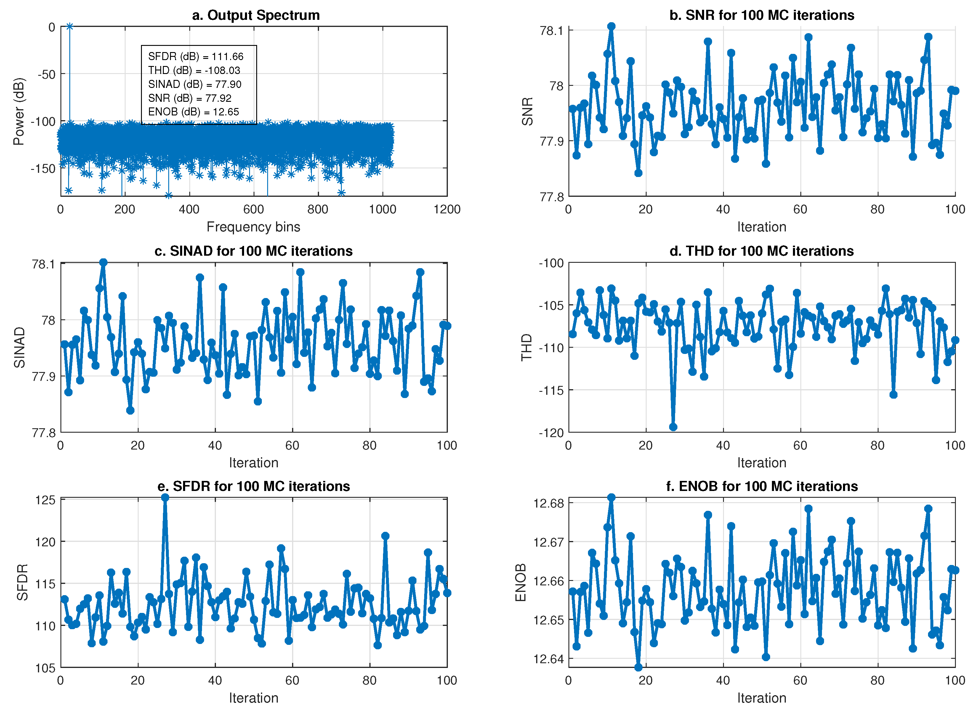
There are two main requirements for the generated sine wave. First, to avoid clipping and obtain high signal power, the peak-to-peak range of the generated waveform was set to be only slightly less than the DAC output range, and coherent sampling is ensured. The total data record length, M, was set to be , and J, the number of sine periods, was set based on Equation (15), which is a well-known equation that must be met to ensure coherency.
where is the signal frequency, and is the sampling frequency. Figure 8a shows the FFT of the generated sine wave for a single iteration. We see that the signal has a signal-to-noise ratio (SNR) of and a signal-to-noise + distortion ratio (SINAD) of , showing that there is just little to no distortion in the signal. The effective number of bits (ENOB) from the SINAD point of view is bits. It must be emphasized that although, the resolution of the DAC is 14-bit, the DAC elements are poorly matched at only the 5-bit level, leading to area and cost savings. The total harmonic distortion (THD) and the spurious free dynamic range (SFDR) is and respectively.
To show robustness of the proposed signal generator, 100 random iterations of sine wave is generated. Figure 8b,c show SNR and SINAD for the 100 samples. The worst case for both SNR and SINAD is greater than is . Also, the worst case THD and SFDR are less than and respectively as shown in Figure 8d,e. It is evident from Figure 8 that the variations affect the THD and SFDR more than the SNR and SINAD. This is because the THD and SFDR have a strong dependence on the matching of the DAC. The SNR is more dependent on the signal power, which is not affected by matching. Figure 8f. shows that across all the 100 iterations, we are able to achieve a signal with an ENOB of bit from a DAC matched at only the 5-bit level.
5. Discussions
The results from the previous section confirm the effectiveness of the proposed signal generator. The accuracy of the DAC and ADC linearity estimations demonstrates the performance of the proposed scheme. To achieve a similar performance using the standards set by IEEE [19], we would require DACs and ADCs with more than 20-bit resolution, making our approach very cost effective. The two calibration methods: pre-distortion and optimal search, both achieve excellent DAC and ADC linearity performance within LSBs. Notably, the pre-distortion method is shown to be nearly as effective as the optimal search while offering significant memory and cost efficiency. The proposed DAC achieves linearity while using only of the area that would be used to achieve the same linearity using the conventional R2R DAC. The design has been summarized in the previous sections, however readers are suggested to refer to [28] for a more rigorous analysis and design of the DAC.
Furthermore, the spectral analysis validates the improved signal purity following the pre-distortion calibration, highlighting the technique’s robustness even when using a poorly matched DAC. The results from generated sine wave show a high SNR and SINAD with minimal distortion, underscoring the signal generator’s capability to achieve high performance. The robustness of the proposed design is further evidenced by the consistency of the SNR, SINAD, and THD across 100 iterations, with only minor variation in THD and SFDR, which are more sensitive to matching. Achieving an ENOB of 12.6 bits from a DAC matched at the 5-bit level showcases the efficiency of the design in reducing area and cost without compromising performance.
Table 1 shows a comparison of the proposed signal generator to the state-of-the-art methods.
The table clearly shows that the proposed approach delivers excellent results with significantly relaxed DAC matching requirements, leading to area and cost reductions. Similar to the method in [22], our approach incorporates built-in self-test capabilities while maintaining strong performance. However, our method achieves a signal with much higher purity, despite utilizing less area and being implemented in a less advanced process technology node.
6. Conclusions
This paper presented a novel, cost-effective approach for generating low-distortion waveforms without the need for high-precision instrumentation. By leveraging a low-cost DAC and applying pre-distortion based on the estimated non-linearity of the DAC, we successfully canceled out the inherent non-linearity of the DAC, achieving high-purity waveform generation. The method’s flexibility enables precise generation of other waveforms, making it suitable for various signal generation applications. Through comprehensive simulation results, we validated the effectiveness of this technique, demonstrating that the approach achieves excellent performance even with relaxed DAC matching requirements. This significantly reduces the area and cost, making it an attractive solution for low-cost, high-purity signal generation in practical applications. The generated signals, characterized by high signal-to-noise ratios (SNR) and low distortion, offer a reliable and efficient way to facilitate accurate testing of analog and mixed-signal (AMS) circuits. Future work includes tape-out and fabrication of test chip and testing the performance of the proposed scheme. This method has the potential to be integrated into built-in self-test (BIST) frameworks, further enhancing the ease and affordability of AMS testing.
Funding
This research was funded in part by the Semiconductor Research Corporation (SRC) under task AMS-CSD 3160.012
Data Availability Statement
Most relevant information is provided in the article. Please contact the corresponding author for further enquiries or information including simulation data or/and codes.
Conflicts of Interest
The authors declare no conflicts of interest.
References
- Burns, M.; Roberts, G.W. An Introduction to Mixed-Signal IC Test and Measurement. Oxford University Press, 2000.
- Pavlidis, A.; Louërat, M.-M.; Faehn, E.; Kumar, A.; Stratigopoulos, H.-G. SymBIST: Symmetry-Based Analog and Mixed-Signal Built-In Self-Test for Functional Safety. IEEE Transactions on Circuits and Systems I: Regular Papers 2021, 68, 2580–2593. [CrossRef]
- Mishra, P.; Farahmandi, F. Post-Silicon Validation and Debug. Springer, 2019, 301.
- Brindley, K. Automatic Test Equipment. Elsevier, Amsterdam, The Netherlands, 2013, October.
- R. R. Cordesses and B. Murmann, "Analog-to-Digital Converter Testing," in Maxim Integrated Application Note 6803, 2014. [Online]. Available: https://www.maximintegrated.com.
- "IEEE Standard for Terminology and Test Methods for Analog-to-Digital Converters," IEEE Std 1241-2010 (Revision of IEEE Std 1241-2000), pp.1-139, Jan. 14, 2011, . [CrossRef]
- Maeda, A. A Method to Generate a Very Low Distortion, High Frequency Sine Waveform Using an AWG. In Proceedings of the 2008 IEEE International Test Conference, Santa Clara, CA, USA, 2008, pp. 1–8. [CrossRef]
- Vasan, B. K.; Sudani, S. K.; Chen, D. J.; Geiger, R. L. Low-Distortion Sine Wave Generation Using a Novel Harmonic Cancellation Technique. IEEE Transactions on Circuits and Systems I: Regular Papers 2013, 60, 1122–1134. [CrossRef]
- Malloug, H.; Barragan, M. J.; Mir, S. Practical harmonic cancellation techniques for the on-chip implementation of sinusoidal signal generators for mixed-signal BIST applications. J. Electron. Test. 2018, 34, 263–279. [CrossRef]
- Sato, K.; et al. Low Distortion Sinusoidal Signal Generator with Harmonics Cancellation Using Two Types of Digital Pre-distortion. In Proceedings of the 2023 IEEE International Test Conference (ITC), Anaheim, CA, USA, 2023, pp. 47–55. [CrossRef]
- Katayama, S.; et al. Low Distortion Sine Wave Generator With Simple Harmonics Cancellation Circuit and Filter for Analog Device Testing. IEICE Electronics Express 2023, 20, 20220470.
- Elsayed, M. M.; Sanchez-Sinencio, E. A Low THD, Low Power, High Output-Swing Time-Mode-Based Tunable Oscillator Via Digital Harmonic-Cancellation Technique. IEEE Journal of Solid-State Circuits 2010, 45, 1061–1071. [CrossRef]
- Suryavanshi, R.; Sridevi, S.; Amrutur, B. A comparative study of direct digital frequency synthesizer architectures in 180nm CMOS. In Proceedings of the 2017 International Conference on Microelectronic Devices, Circuits and Systems (ICMDCS), Vellore, India, 2017, pp. 1–5. [CrossRef]
- Ryabov, I. V. Pryamoy tsifrovoy sintez signalov dlya zadach radiolokatsii, navigatsi i svyazi [Direct Digital Synthesis of Signals for Tasks of Radiolocation, Navigation and Communication]. Yoshkar-Ola: VSUT, 2016, 151 p.
- Bochkarev, D. N.; Ryabov, I. V.; Strelnikov, I. V.; Degtyarev, N. V. Direct Digital Synthesizers of Frequency and Phase-Modulated Signals. In Proceedings of the 2019 Systems of Signal Synchronization, Generating and Processing in Telecommunications (SYNCHROINFO), Russia, 2019, pp. 1–4. [CrossRef]
- Strelnikov, I. V.; Ryabov, I. V.; Klyuzhev, E. S. Direct Digital Synthesizer of Phase-Manipulated Signals, Based on the Direct Digital Synthesis Method. In Proceedings of the 2020 Systems of Signal Synchronization, Generating and Processing in Telecommunications (SYNCHROINFO), Svetlogorsk, Russia, 2020, pp. 1–3. [CrossRef]
- Irfansyah, A. Sine wave synthesis with harmonic-cancellation and single-bit sigma-delta modulation. In Proceedings of the International Symposium on Electronics Smart Devices (ISESD), Oct. 2017, pp. 150–153.
- Huang, J.; Zhou, T.; Liu, H.; Qi, L.; Yan, L.; Li, Y. Low Noise, High Linearity Sine Wave Generation Using Noise-Shaping Phase-Switching Technique. IEEE Transactions on Instrumentation and Measurement 2021, . [CrossRef]
- IEEE Standard for Digitizing Waveform Recorders. IEEE Std 1057-2017 (Revision of IEEE Std 1057-2007) 2018, pp. 1–0. [CrossRef]
- Zhuang, Y.; Unnithan, A.; Joseph, A.; Sudani, S.; Magstadt, B.; Chen, D. Low cost ultra-pure sine wave generation with self calibration. In Proceedings of the 2016 IEEE International Test Conference (ITC), Phoenix, AZ, USA, 2016, pp. 1–9. [CrossRef]
- Zhuang, Y.; Magstadt, B.; Chen, T.; Chen, D. High-Purity Sine Wave Generation Using Nonlinear DAC With Predistortion Based on Low-Cost Accurate DAC–ADC Co-Testing. IEEE Transactions on Instrumentation and Measurement 2018, 67, 279–287. [CrossRef]
- Bhatheja, K.; et al. Low Cost High Accuracy Stimulus Generator for On-chip Spectral Testing. In Proceedings of the 2022 IEEE International Test Conference (ITC), Anaheim, CA, USA, 2022, pp. 514–518. [CrossRef]
- M. J. M. Pelgrom, A. C. J. Duinmaijer, and A. P. G. Welbers, "Matching properties of MOS transistors," in IEEE Journal of Solid-State Circuits, vol. 24, no. 5, pp. 1433-1439, Oct. 1989, . [CrossRef]
- M. Pelgrom, Analog-to-Digital Conversion, Cham: Springer International Publishing, 2017.
- M. P. Kennedy, "On the robustness of R-2R ladder DACs," in IEEE Transactions on Circuits and Systems I: Fundamental Theory and Applications, vol. 47, no. 2, pp. 109-116, Feb. 2000, . [CrossRef]
- T. Bharath, R. Narula, and P. Tadeparthy, "Generalized Resistive DAC Analysis Through Unitized T-Network Element," in 2022 IEEE International Symposium on Circuits and Systems (ISCAS), Austin, TX, USA, 2022, pp. 2797-2801, . [CrossRef]
- Bhatheja, K.; Chaganti, S.; Leisinger, J.; Darko, E. N.; Bruce, I.; Chen, D. A BIST Approach to Approximate Co-Testing of Embedded Data Converters. IEEE Design & Test 2024. [CrossRef]
- Sekyere, M.; Darko, E. N.; Bruce, I.; Odion, E. O.; Bhatheja, K.; Chen, D. Ultra-Small Area, Highly Linear Sub-Radix R-2R Digital-To-Analog Converters with Novel Calibration Algorithm. In Proceedings of the 2023 IEEE 66th International Midwest Symposium on Circuits and Systems (MWSCAS), Tempe, AZ, USA, 2023, pp. 604–608. [CrossRef]
Figure 1.
Overall architecture of the proposed arbitrary waveform generator.
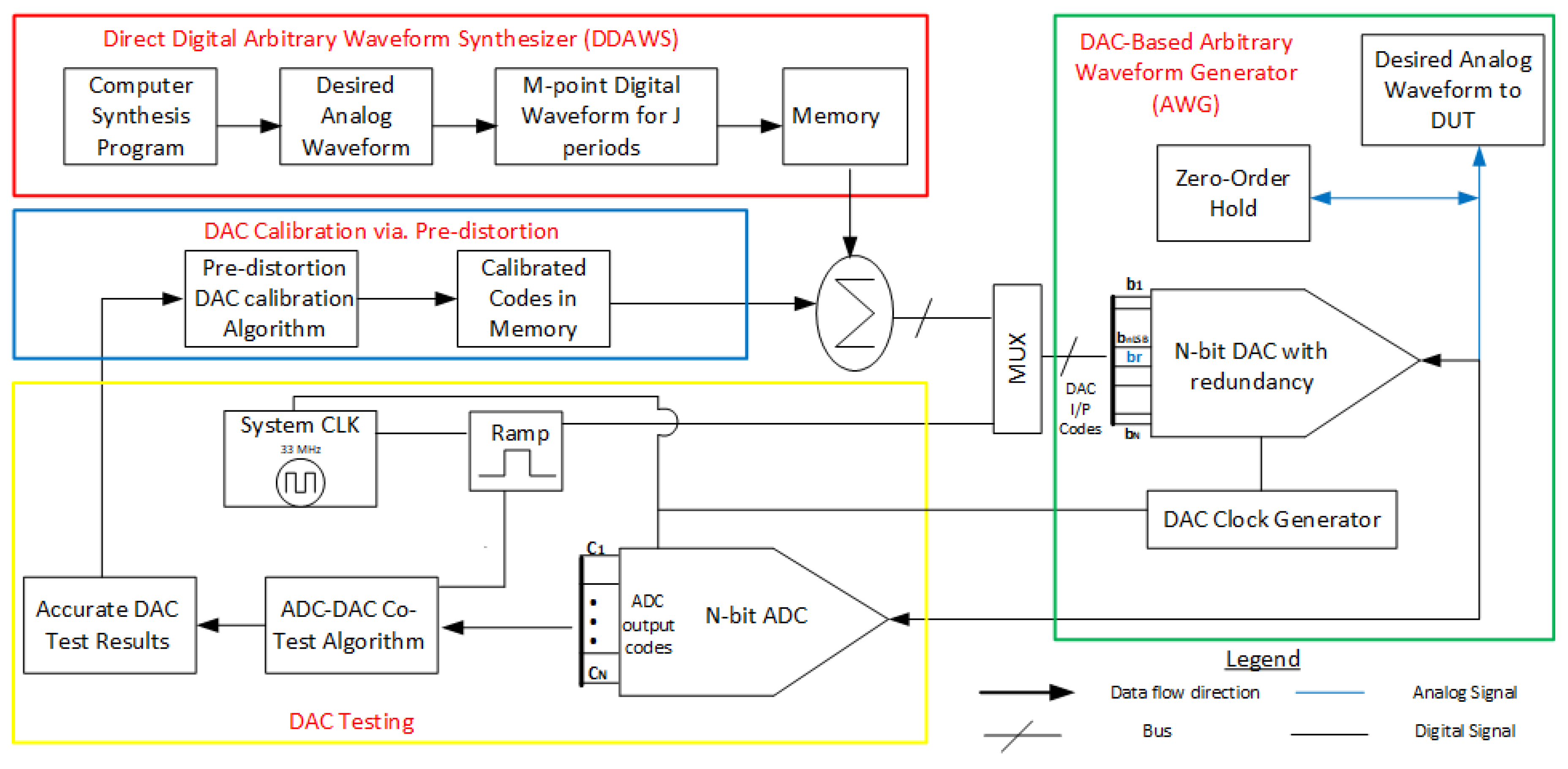
Figure 2.
Proposed DAC used for waveform generation
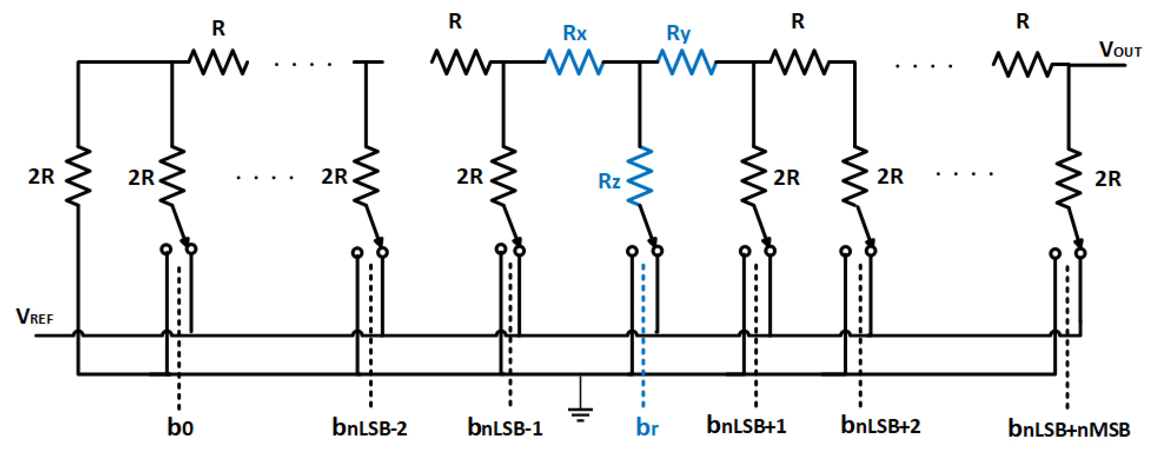
Figure 3.
ADC DAC co-test Scheme
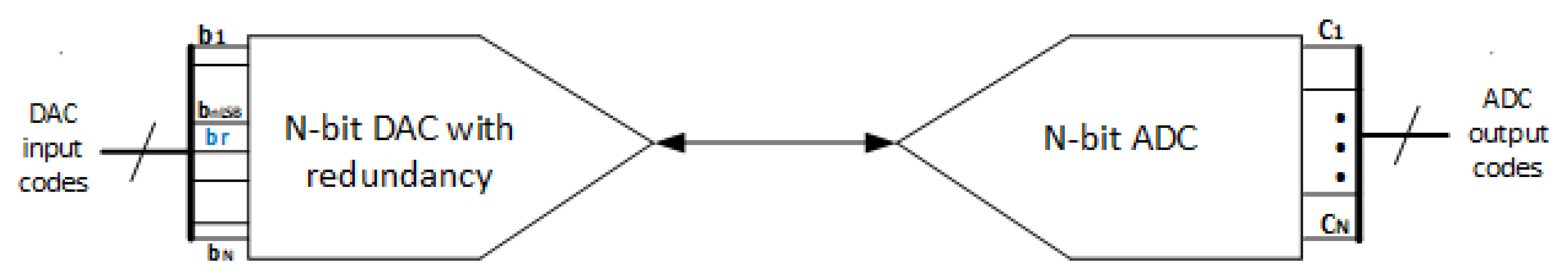
Figure 4.
Layout of proposed DAC. We use cheap poly resistors which are known to have temperature and voltage co-efficients, whilst matching them at only the 5-bit level. Dimensions is resulting in a total area of
Figure 4.
Layout of proposed DAC. We use cheap poly resistors which are known to have temperature and voltage co-efficients, whilst matching them at only the 5-bit level. Dimensions is resulting in a total area of
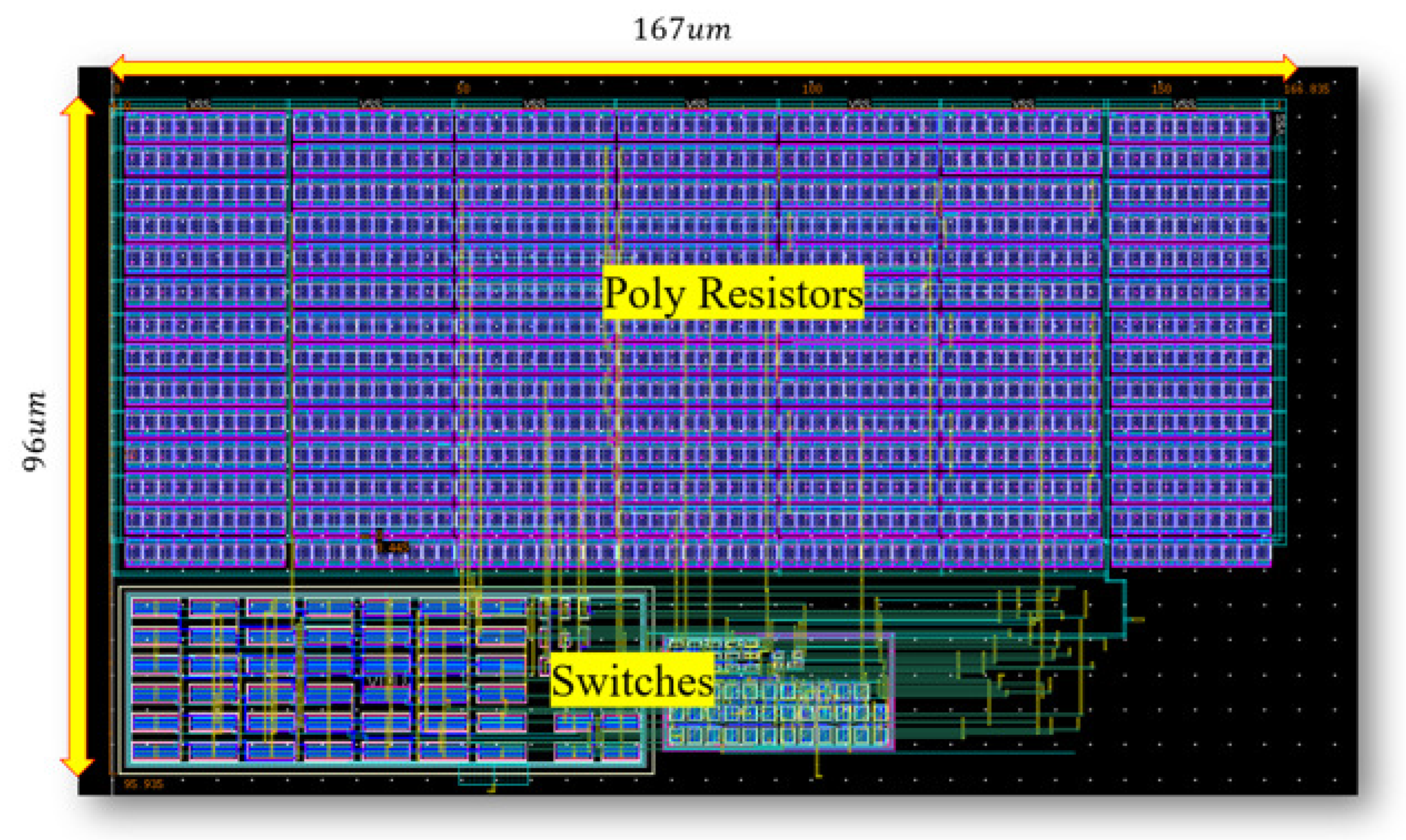
Figure 5.
The red box shows the DAC Layout in the pad frame. We can see that the area is very small and almost equivalent to about the area of a single pad.
Figure 5.
The red box shows the DAC Layout in the pad frame. We can see that the area is very small and almost equivalent to about the area of a single pad.
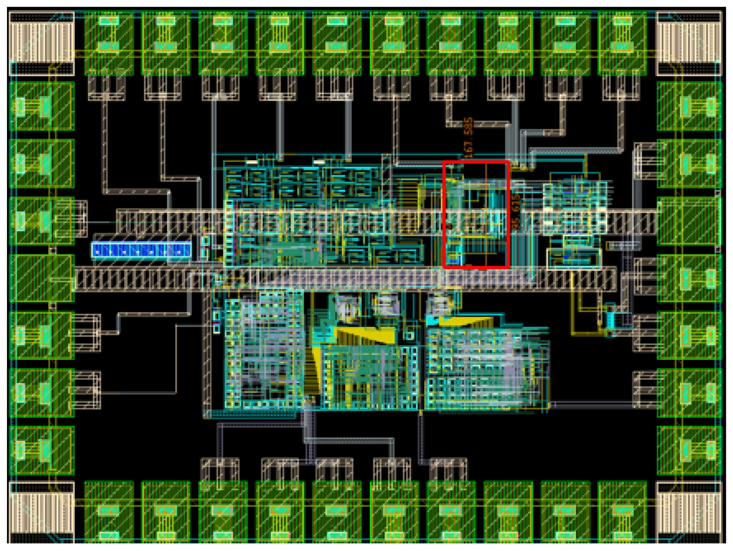
Figure 6.
Results from the simultaneous testing of the ADC and DAC. a. True and Estimated DAC INL Estimated weight of the redundant bit is b. DAC INL Estimation Error c. True and Estimated SAR ADC INL d. ADC INL Estimation Error. From 4b and 4d, it can be seen that the maximum absolute DAC and ADC INL abre both less than .

Figure 7.
Comparison of performance between the search and proposed pre-distortion calibration. a. Search vrs pre-distortion calibration INL b. DAC Output spectrum before and after pre-distortion
Figure 7.
Comparison of performance between the search and proposed pre-distortion calibration. a. Search vrs pre-distortion calibration INL b. DAC Output spectrum before and after pre-distortion
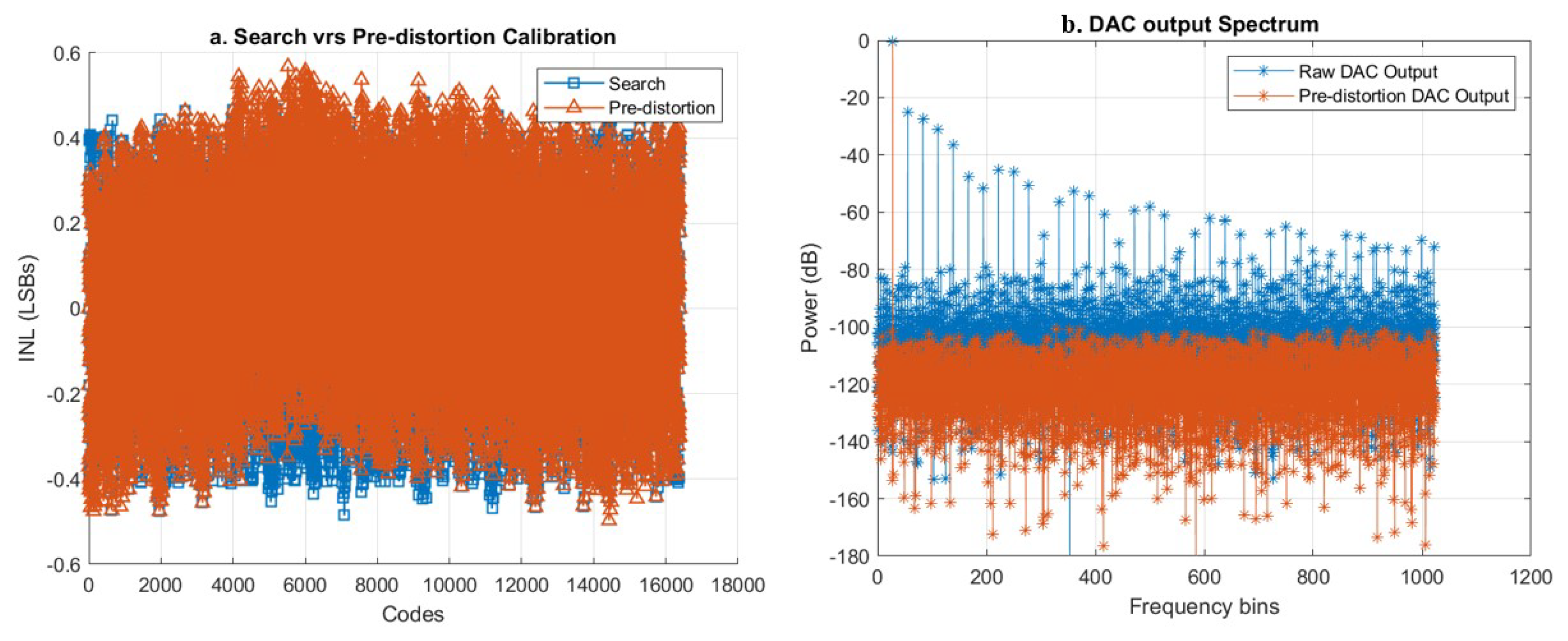
Figure 8.
Results showing the purity of the generated signal. a. Spectrum of generated sine wave b. SNR of sine wave for 100 iterations c. SINAD of sine wave for 100 iterations d. THD of sine wave for 100 iterations e. SFDR of sine wave for 100 iterations f. ENOB of sine wave for 100 iterations
Figure 8.
Results showing the purity of the generated signal. a. Spectrum of generated sine wave b. SNR of sine wave for 100 iterations c. SINAD of sine wave for 100 iterations d. THD of sine wave for 100 iterations e. SFDR of sine wave for 100 iterations f. ENOB of sine wave for 100 iterations

Disclaimer/Publisher’s Note: The statements, opinions and data contained in all publications are solely those of the individual author(s) and contributor(s) and not of MDPI and/or the editor(s). MDPI and/or the editor(s) disclaim responsibility for any injury to people or property resulting from any ideas, methods, instructions or products referred to in the content. |
© 2024 by the authors. Licensee MDPI, Basel, Switzerland. This article is an open access article distributed under the terms and conditions of the Creative Commons Attribution (CC BY) license (http://creativecommons.org/licenses/by/4.0/).
Copyright: This open access article is published under a Creative Commons CC BY 4.0 license, which permit the free download, distribution, and reuse, provided that the author and preprint are cited in any reuse.


