1. Introduction
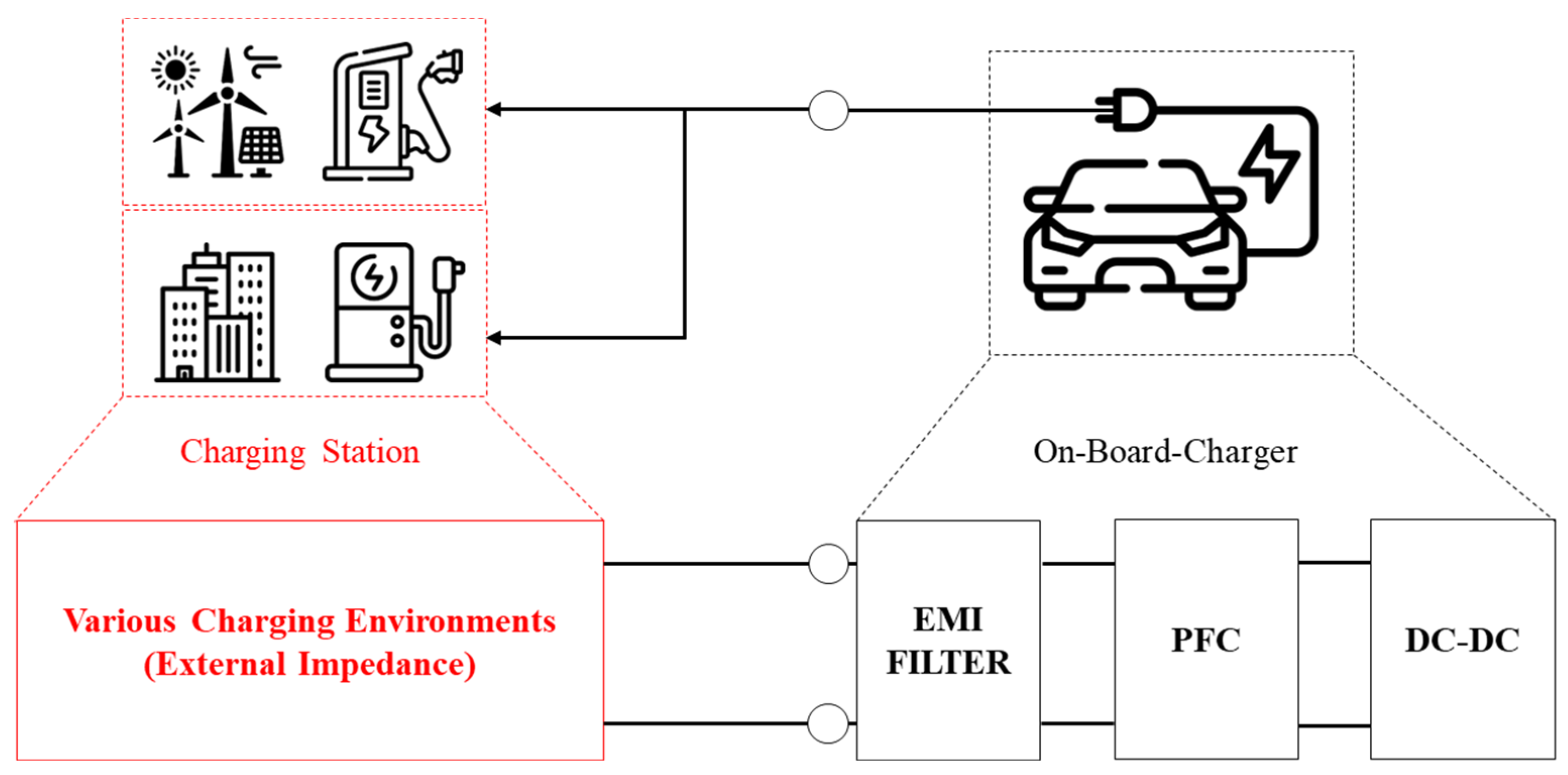
The charging system installed in electric vehicles typically comprises three components, as illustrated in
Figure 1: an Electromagnetic Interference (EMI) filter for compliance with electromagnetic regulations, a Power Factor Correction (PFC) circuit for reactive power compensation, and a DC-DC circuit to meet a wide output voltage range.
Electric vehicles charge at various charging stations depending on the situation. Therefore, the charging system of an electric vehicle, unlike conventional power conversion devices, encounters various external impedances (External block in
Figure 1). Such external impedances affect the response characteristics and stability of the charging system. To ensure the reliability of the charging system, it is necessary to assess the stability based on the external impedance.
In this paper, for the sake of simplicity, the stability of the DC-DC circuit within the charging system is assumed to be stable. Subsequently, the stability of the system, composed of external impedance, EMI filter, and boost PFC, is analyzed. Specifically, The stability is determined by employing the relationship between the output impedance, which includes external impedance and the EMI filter, and the input impedance of the boost PFC, similar to the approach taken in the study by R. D. Middlebrook [
1].
2. Impedance Analysis
In this paper, as shown in
Figure 2, the system is composed of a 2-stage PI filter and a bridgeless totem pole boost PFC converter.
is the output impedance of an EMI filter, and
is the input impedance of the boost PFC.
2.1. EMI Filter Output Impedance with the External Impedance
In this section, discuss the impedance analysis of the EMI filter and explore the impedance analysis when external impedance is considered.
2.1.1. Differential Mode Loop
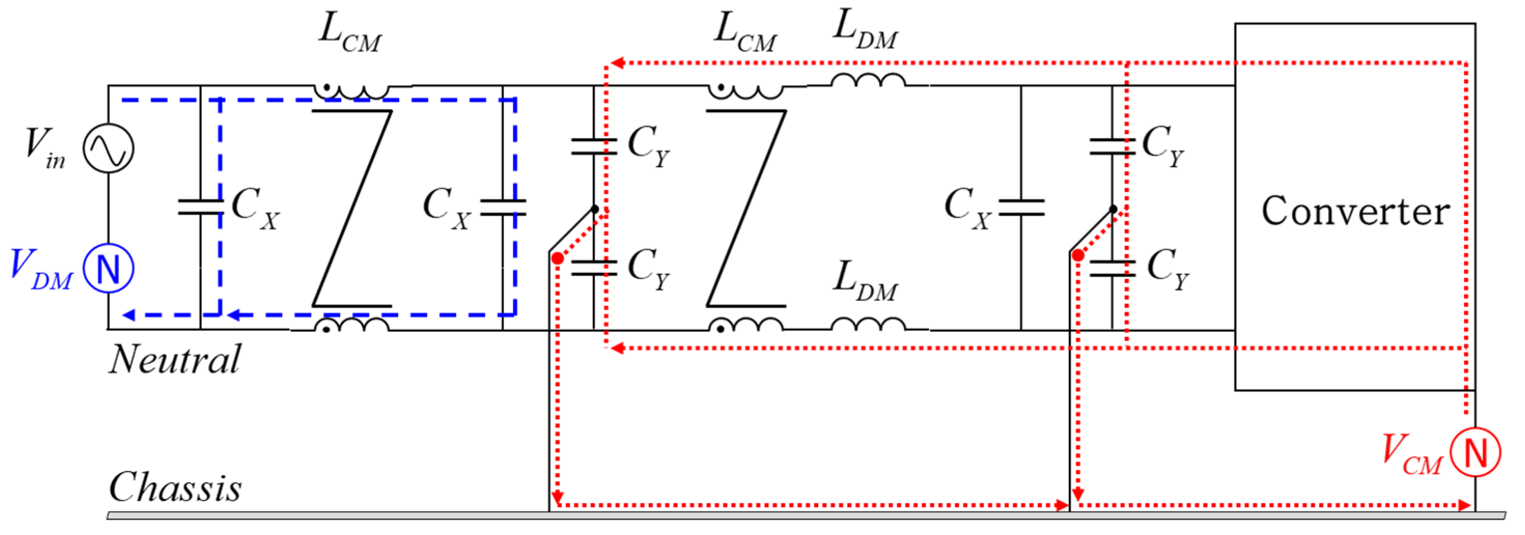
EMI filters are generally classified into two types based on the type of noise : CM (Common Mode) noise and DM (Differential Mode) noise. CM components include CM inductors and Y-capacitors, while DM components include DM inductors and X-capacitors.
Figure 3 illustrates the typical structure of an EMI filter. There is CM noise forming a loop through the chassis and DM noise forming a loop through the neutral line.
Figure 4 depicts the entire EMI filter with a chassis.
Figure 5 represents the circuit of the DM loop.
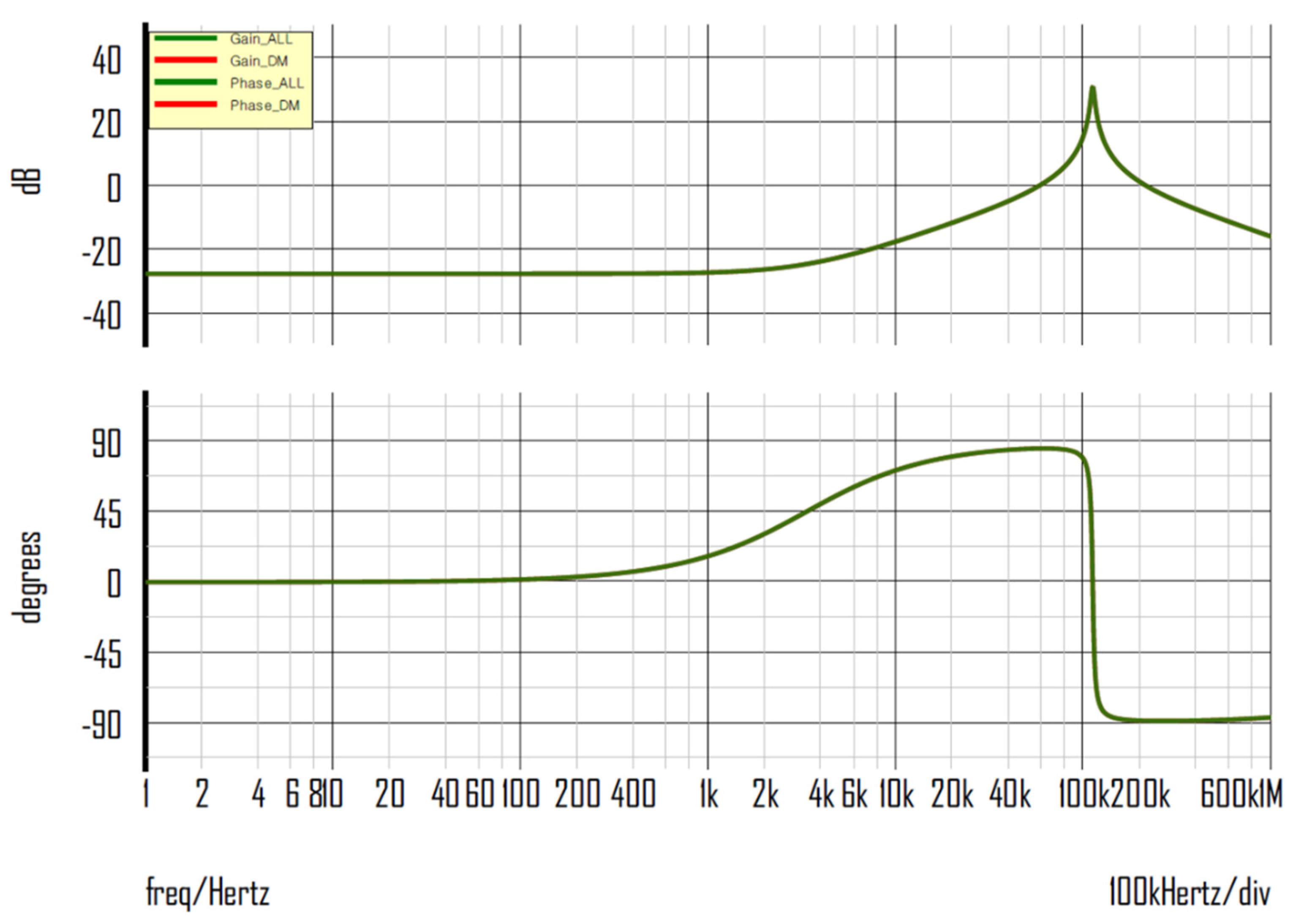
Figure 6 illustrates the input shorted output impedance of the two circuits. The parameters of the EMI filter used in the simulation are indicated in
Table 1.
Even when considering only the components of the DM loop, as shown in
Figure 6, it has the same effect as considering the impedance of the entire circuit. In other words, in the stability analysis of complex EMI filters, the effects of the CM loop can be eliminated to simplify the analysis.
The stability analysis in power conversion devices is defined when input and output form a loop. In the case of the EMI filter, the loop formed by DM noise affects stability. On the contrary, the loop formed by CM noise does not affect stability. Therefore, from the perspective of the EMI filter at the input, only the components forming the loop with the input voltage are considered. In other words, only the X-capacitors related to DM noise are taken into account.
2.1.2. Impedance Analysis with the External Impedance
Generally, the grid impedance of a power system consists of inductive and resistive components. In this paper, the term 'external impedance' is used instead of 'grid impedance' for a more conventional stability analysis.
When external impedance is added, define the impedance
by shorting the voltage source side, not the termination side of the EMI filter, as indicated in
Figure 7.
2.2. Boost PFC Input Impedance
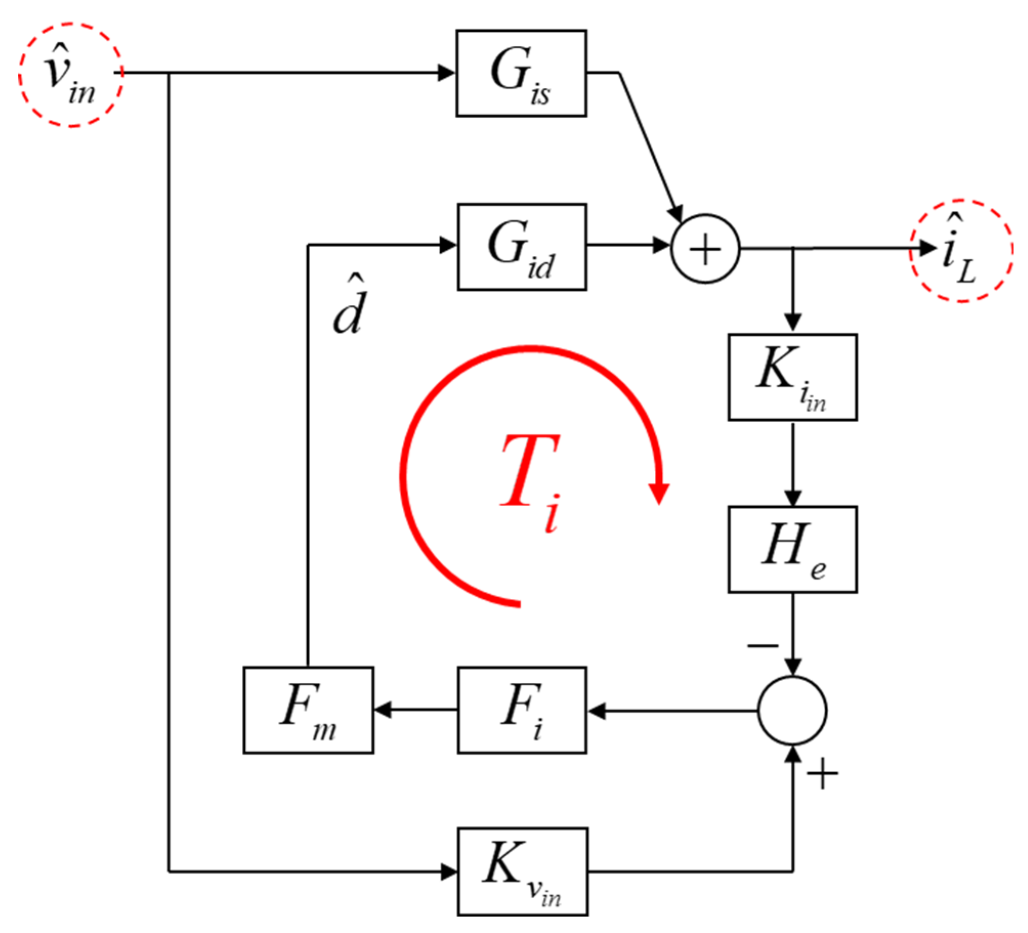
The control block diagram for deriving the input impedance of the boost PFC is illustrated in
Figure 8, and the input impedance is represented by Equation (1). The boost PFC input impedance
is influenced by the current control loop. Assuming that the voltage control loop has a crossover frequency significantly lower than the current control loop crossover frequency, it is considered to have no impact. After the crossover frequency, the Boost PFC inductor leads the phase by +90° [
3].
3. Stability Analysis of Boost PFC Considering the External Impedance
The stability of the system with coupled external impedance is defined by a new characteristic equation, known as the minor loop gain
. The uncoupled loop gain
represents the loop gain of the converter with ideal input and output. It is equivalent to the loop gain commonly used in practice [
10]. For stability analysis considering the influence of the input impedance,
is assumed to be stable, and the minor loop gain
is analyzed.
Using SIMPLIS to simulate in the frequency-domain and time-domain, it was confirmed that determines the stability of the whole system. For the convenience of analysis, the simulation considers only the external impedance, EMI filter, and boost PFC in the OBC system.
The EMI filter consists of a 2-stage PI filter with CM filters, as shown in
Figure 2. The parameters related to the EMI filter are presented in
Table 2. The boost PFC is a Bridgeless Totem Pole Boost PFC converter, as illustrated in
Figure 2. The parameters associated with the boost PFC are presented in
Table 3. For current control and voltage control, a Type II compensator, as represented Equation (2), was implemented..
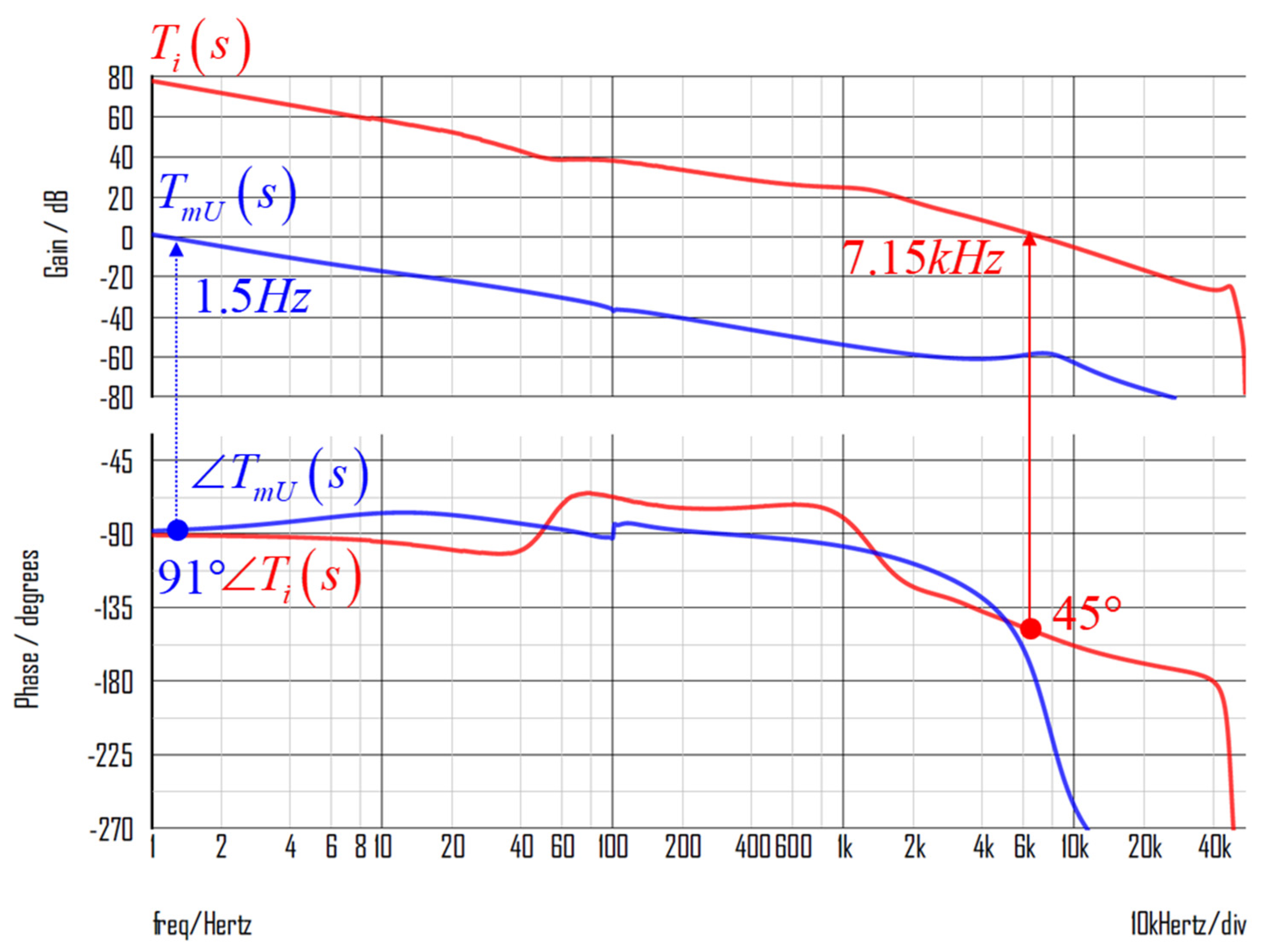
Figure 9 illustrates the current loop gain
and
using the parameters that were mentioned earlier. The crossover frequency of
is 7.15 kHz, and the phase margin is 45°. And The crossover frequency of
is 1.5 Hz, and the phase margin is 91°.
3.1. Stability Criteria with the External Impedance
The minor loop gain
describes the relationship between the output impedance
of an EMI filter with external impedance included, and the input impedance
of a boost PFC. The stability criteria of the minor loop gain can be performed in the same manner as the conventional loop gain. These relationships are represented in equation (3).
Figure 10 depicts the bode plot of
using
and
.
3.2. Converter Performance under System Interaction
While varying the inductance of the external impedance, consider scenarios where the minor loop gain becomes stable or unstable. In this case, the resistance of the external impedance is fixed at 100mΩ.
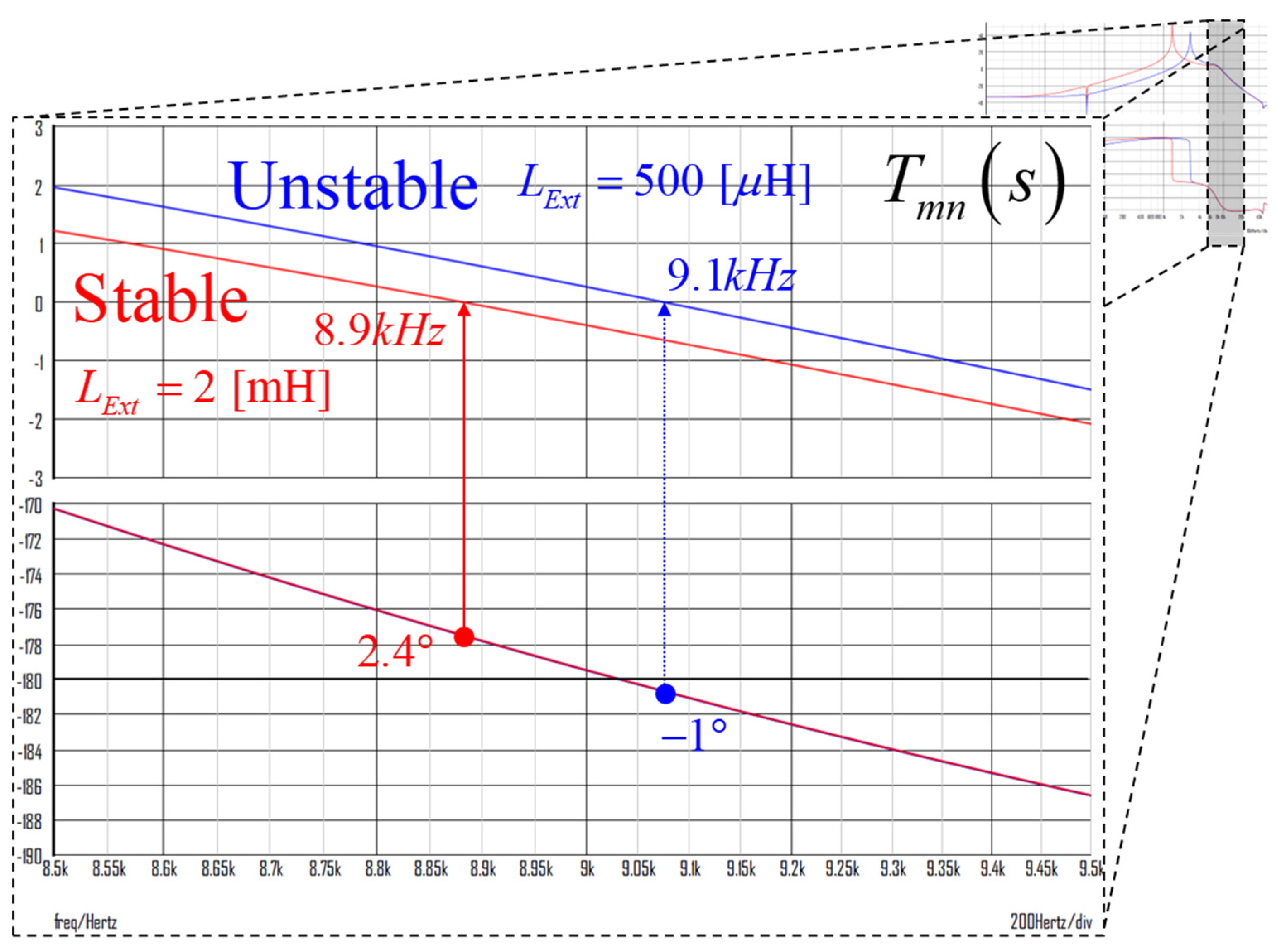
Figure 11 represents the minor loop gain
, while
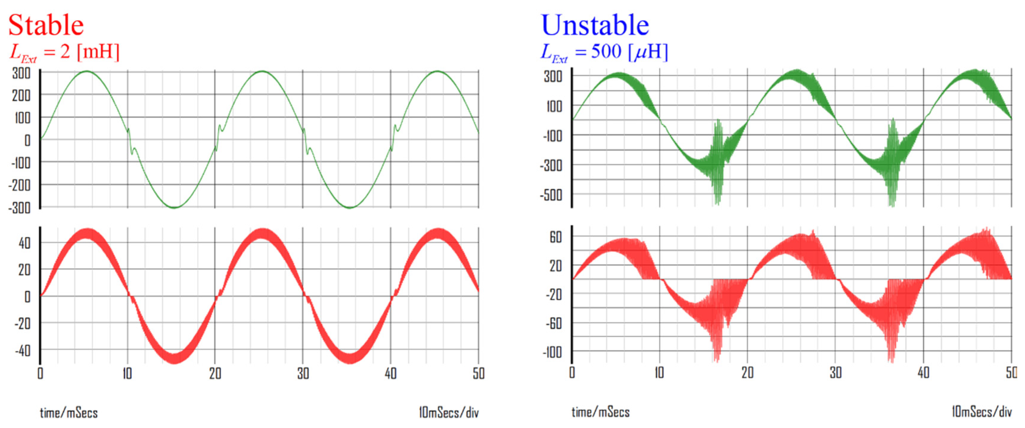
Figure 12 depicts the input voltage and current of the boost PFC.
When is 2mH, the phase margin is 2.4°, system is stable. On the other hand, when is 500uH, the phase margin is -1°, system is unstable. The effectiveness of the stability criteria is confirmed through simulations in both the frequency domain and time domain. As predicted in the frequency domain, in an unstable condition, the input voltage and current resonate. Therefore, it can be concluded that the stability criteria through the minor loop gain is verified.
4. Conclusions
This paper has summarized the stability analysis approach considering external impedance. The relationship between and , in other words, using the minor loop gain , can be employed to determine stability. The results were validated through simulations, confirming the effectiveness of the stability analysis approach. Generally, instability occurs when the phase difference () at the intersection point of two impedances is greater than -180°
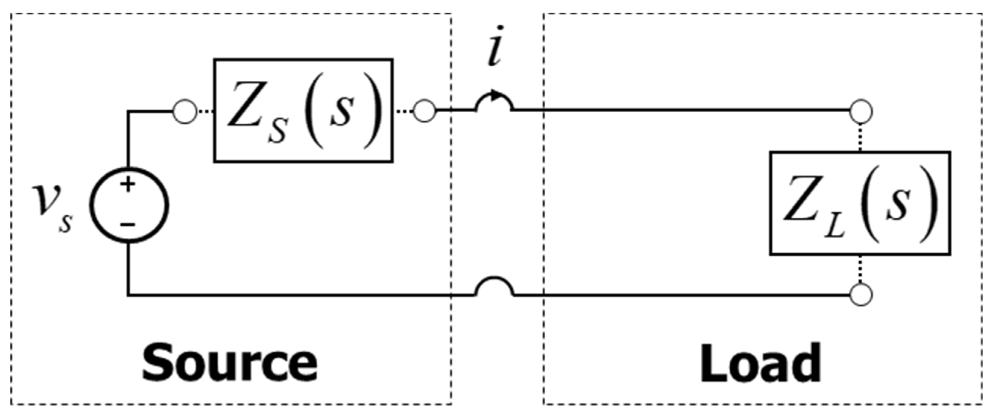
To simplify the explanation for better understanding using circuit theory, it can be described as follows. As depicted in
Figure 13, most power conversion devices are divided into a source and a load. And there are source impedance and load impedance. If the magnitudes of the source impedance and load impedance are equal, and their phases are opposite, the current will flow to infinity. Therefore, this can be considered as the system being unstable. In the charging system, the source impedance can be thought of as
, and the load impedance as
. Thus, as indicated in equation (4) the minor loop gain
can be defined with the numerator as the source impedance
and the denominator as the load impedance
.
The charging system installed in electric vehicles must operate in various charging environments. The system might become unstable and, in certain situations, could face the possibility of being destroyed. Therefore, an analysis of the impedance specifications for which the system can operate is required. The external impedance of the system is properly quantified and designed based on the stability criteria by analyzing
.
Appendix A: Input Filter Interaction Example with SIMPLIS Elements
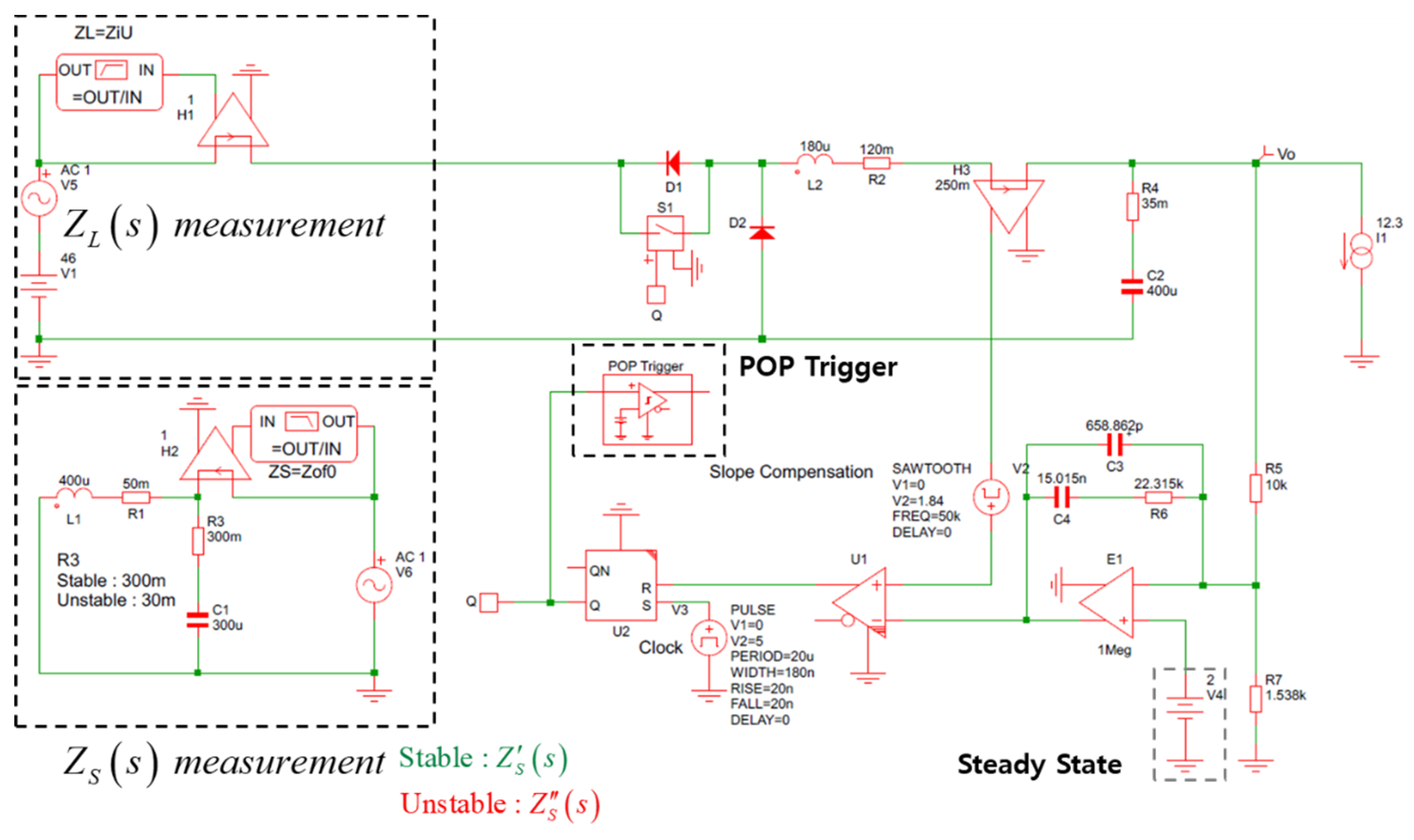
In this section, explain the example from the Conclusion using the SIMPLIS Elements version. In the given example, a Buck converter was employed, and the system interaction was observed by modifying the resistance of the filter. Following the parameters and elements depicted in the figures makes it easy to verify the system interaction.
When configuring the SIMPLIS schematic as shown in
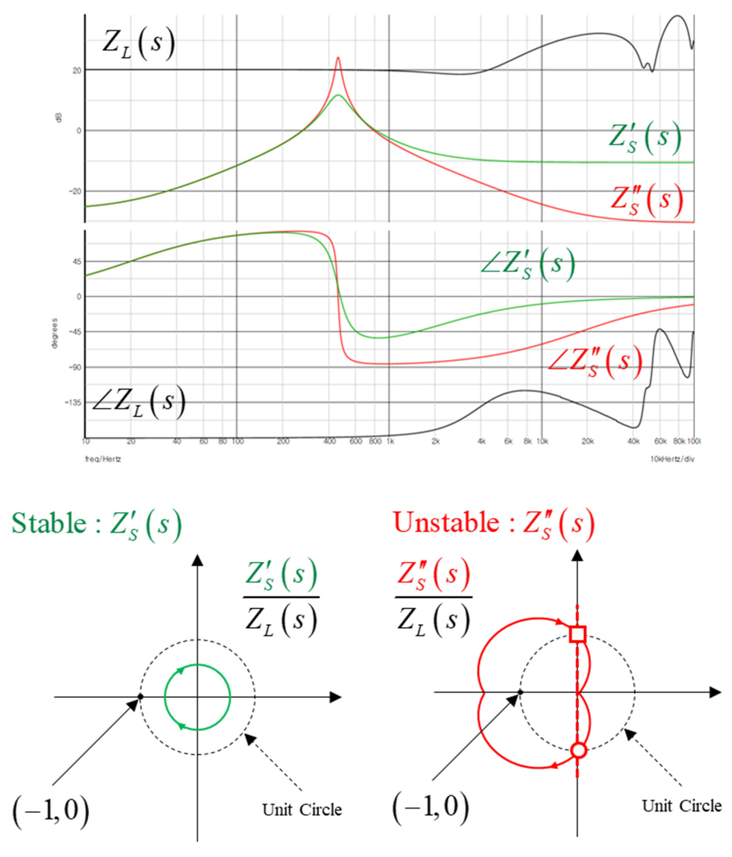
Figure A1, frequency domain measurements become possible. In this case, it is necessary to add SIMPLIS's unique feature, the POP Trigger element. Setting the resistance value R3 of the filter to 300mΩ results in stability, while setting it to 30mΩ leads to instability. Subsequently, the measurement results in the frequency domain are illustrated in
Figure A2.
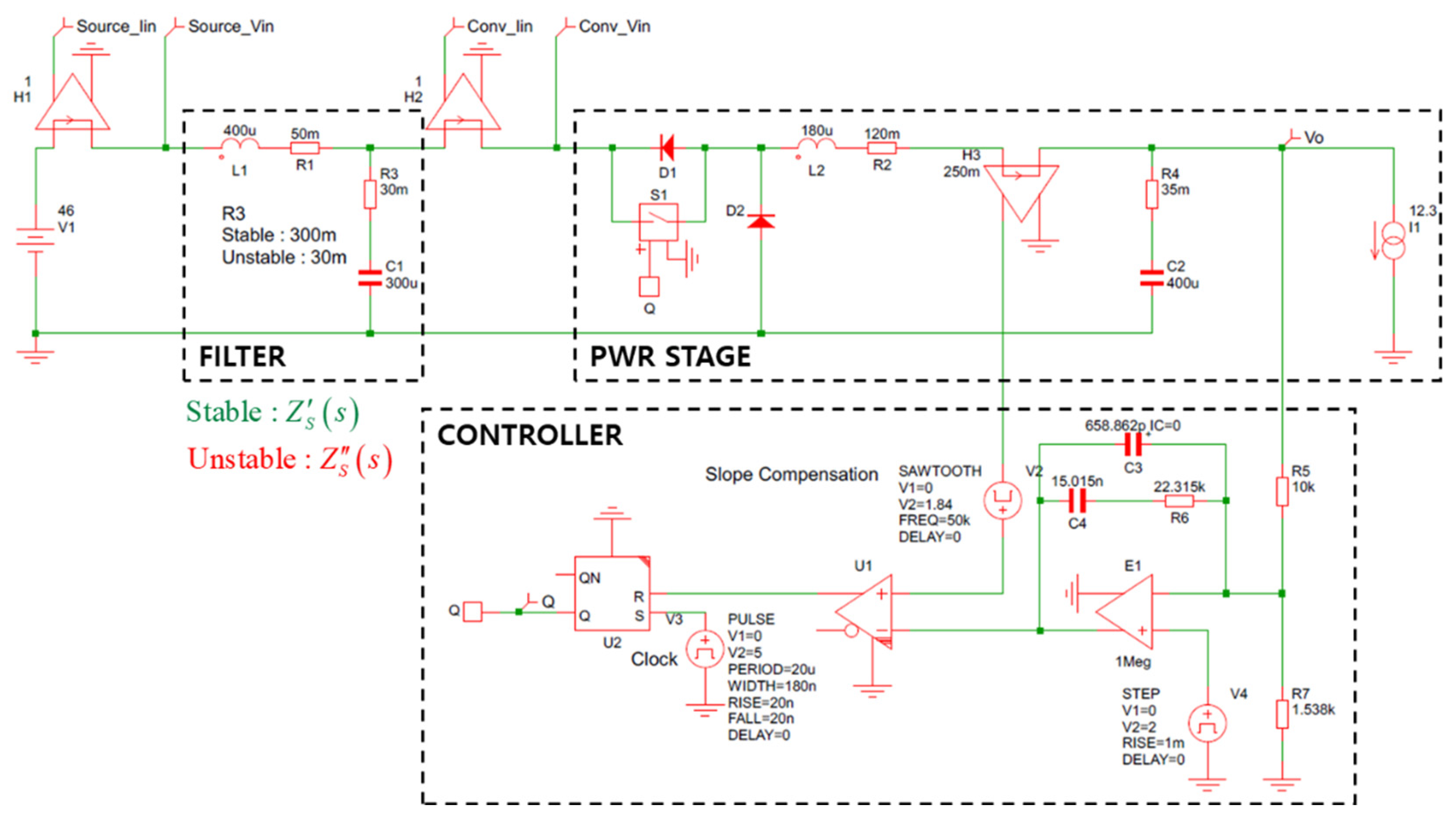
To validate the stability criteria, a time-domain simulation is performed. As illustrated in
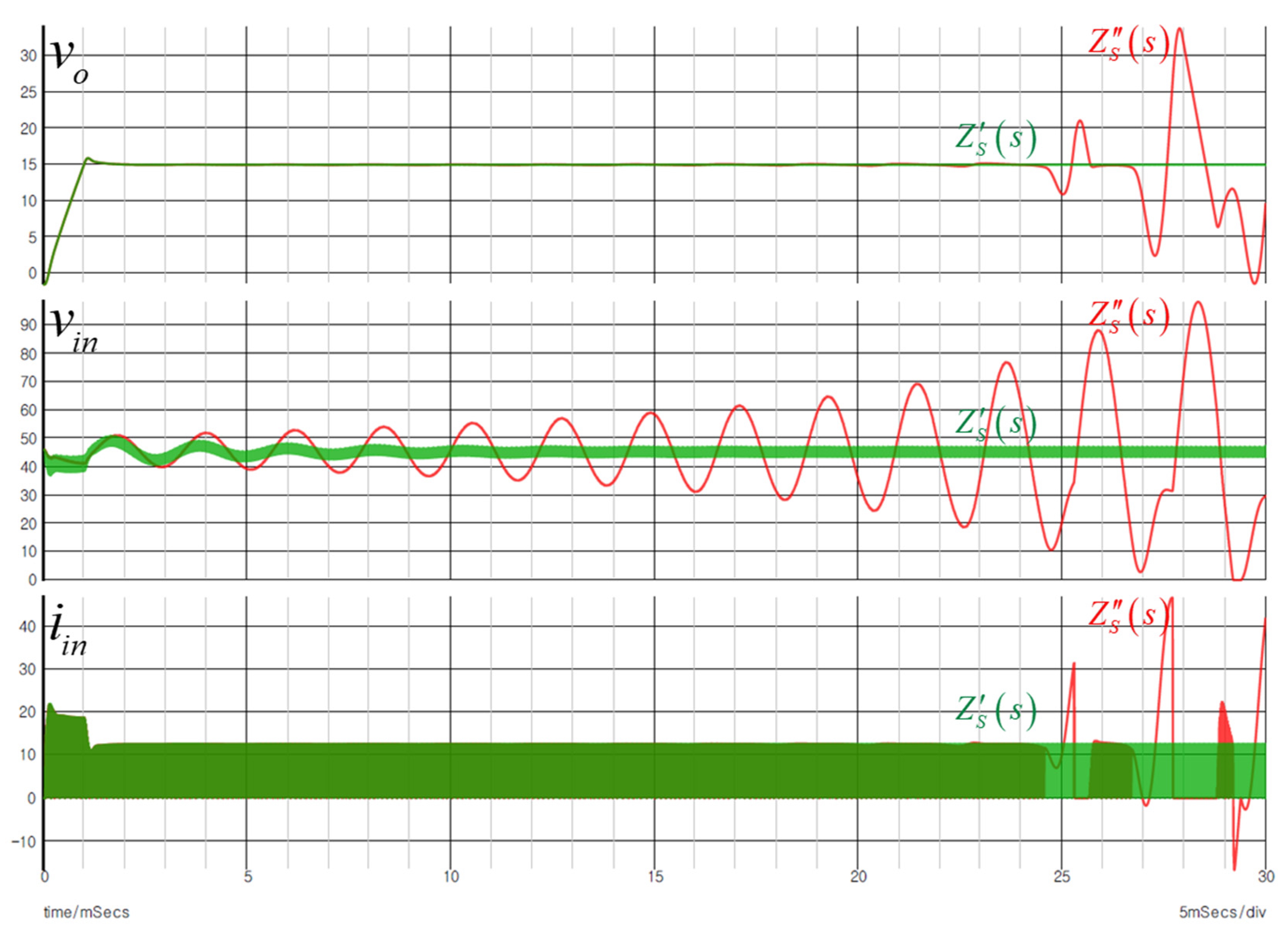
Figure A3, configure the schematic accordingly and perform a transient analysis. The results of the time-domain simulation in
Figure A4 display that in unstable conditions, the input and output voltages and currents exhibit divergence.
Figure A1.
SIMPLIS schematic for frequency domain measurements.
Figure A1.
SIMPLIS schematic for frequency domain measurements.
Figure A2.
The stability criteria in frequency domain of buck converter.
Figure A2.
The stability criteria in frequency domain of buck converter.
Figure A3.
SIMPLIS schematic for time domain measurements.
Figure A3.
SIMPLIS schematic for time domain measurements.
Figure A4.
Converter performance in time domain of buck converter.
Figure A4.
Converter performance in time domain of buck converter.
References
- R. D. Middlebrook, Input filter considerations in design and application of switching regulators, in Conf. Rec. IEEE-IAS Annu. Meeting, 1976, pp. 366-382.
- R. D. Middlebrook, Measurement of loop gain in feedback systems†, International Journal of Electronics, vol. 38, no. 4. Informa UK Limited, pp. 485–512, Apr-1975.
- J. Sun, Input Impedance Analysis of Single-Phase PFC Converters, IEEE Transactions on Power Electronics, vol. 20, no. 2. Institute of Electrical and Electronics Engineers (IEEE), pp. 308–314, Mar-2005.
- Pidaparthy, S.K.; Choi, B. Input Impedances of PWM DC-DC Converters: Unified Analysis and Application Example, Journal of Power Electronics, vol. 16, no. 6. The Korean Institute of Power Electronics, pp. 2045–2056, 20-Nov-2016. [CrossRef]
- Spiazzi, G.; Pomilio, J. Interaction between EMI filter and power factor preregulators with average current control: analysis and design considerations, APEC ’99. Fourteenth Annual Applied Power Electronics Conference and Exposition. 1999 Conference Proceedings (Cat. No.99CH36285). IEEE, 1999. [CrossRef]
- Huliehel, F.; Lee, F.; Cho, B. Small-signal modeling of the single phase boost high power factor converter with constant frequency control, in Proc. IEEE PESC, 1992, pp. 475-482.
- Shin, J.-W.; Cho, B.-H. Digitally Implemented Average Current-Mode Control in Discontinuous Conduction Mode PFC Rectifier, IEEE Trans. Power Electron., vol. 27, no. 7, pp. 3363-3373, Jul. 2012. [CrossRef]
- R. B. Ridley, A New Small-Signal Model for Current Mode Control, Ph. D. Dissertation, Virginia Polytechnic Institute and State University, Blacksburg, VA, Nov. 1990.
- Tang, W.; Lee, F.; Ridley, R. Small-signal modeling of average current mode control, IEEE Trans. on Power Electron., vol. 8, no. 2, pp.112-119, Apr. 1993.
- Byungcho Choi, Pulsewidth Modulated DC-to-DC Power Conversion: Circuits, Dynamics, Control, and DC Power Distribution Systems, 2nd ed., Wiley-IEEE Press, 2021.
|
Disclaimer/Publisher’s Note: The statements, opinions and data contained in all publications are solely those of the individual author(s) and contributor(s) and not of MDPI and/or the editor(s). MDPI and/or the editor(s) disclaim responsibility for any injury to people or property resulting from any ideas, methods, instructions or products referred to in the content. |
© 2024 by the authors. Licensee MDPI, Basel, Switzerland. This article is an open access article distributed under the terms and conditions of the Creative Commons Attribution (CC BY) license (https://creativecommons.org/licenses/by/4.0/).
