1. Introduction
Temperature sensors are extensively utilized across various fields, including industry, healthcare, environmental monitoring, aerospace, and automotive applications. However, traditional temperature sensors, including thermocouples[
1,
2], thermistors[
3,
4], and infrared sensors[
5,
6], often demonstrate slow response times, limited measurement ranges, insufficient accuracy, and susceptibility to environmental interference, severely restricting their practical applications. Terahertz (THz) waves possess unique electromagnetic properties that enable them to penetrate various non-metallic materials[
7,
8,
9]. The high-frequency characteristics of THz waves facilitate faster response times in sensors. Consequently, the THz frequency range can be utilized in temperature sensors for non-contact measurements, thereby avoiding errors and damage associated with traditional sensors that require contact with the measured object[
10,
11,
12]. However, the weak response of THz waves to natural materials significantly hinders their development. Metamaterials, composed of periodically arranged sub-wavelength unit structures, exhibit exceptional physical properties that are not present in natural materials[
13,
14,
15,
16]. By designing suitable metamaterial structures, a strong response to THz waves can be achieved, thereby enhancing the performance of temperature sensors[
9,
17,
18,
19,
20,
21,
22].
In THz metamaterial temperature sensors, temperature-sensitive materials are typically chosen as the modulation medium, including strontium titanate based on the damped resonator model[
23,
24], graphene based on Falkovsky's formula[
25,
26], and InSb based on Drude's model[
27,
28] etc. Changes in ambient temperature induce variations in dielectric properties, which subsequently affect THz wave transmission performance. For instance, D. Li et al. [
24] investigated the potential of using strontium titanate for temperature sensing based on a perfect absorber of terahertz metamaterials, which consists of two split-ring resonators of different sizes, a silicon substrate, and a bottom metallic layer. The frequency of the absorption peaks can be blue-shifted from 1.41 to 1.52 THz as the temperature increases from 200 to 400 K. This setup achieves a temperature sensitivity of 0.00055 THz/K. Utilizing the temperature-sensitive properties of InSb materials, T.T. Lang et al. [
29] developed a temperature sensor with a sensitivity of 21.9 GHz/K, employing a perfect absorber of terahertz metamaterials. A. Keshavarz et al. [
26] reported a nanoscale terahertz metamaterial composed of a graphene H-shape situated on an InSb substrate. Given that the optical properties of graphene and InSb are highly temperature-dependent, the resonance frequency shifts with temperature changes, allowing for temperature sensing with a sensitivity of 0.027 THz/K. Despite existing studies on THz metamaterial temperature sensors, challenges such as low sensitivity and measurement accuracy persist. Furthermore, achieving unique resonant responses requires complex designs of metamaterial unit structures, resulting in challenges in analysis, design, and fabrication.
Vanadium dioxide (VO₂) is a material that undergoes a reversible insulator-metal phase transition at approximately 68°C[
30]. During this transition, VO₂ undergoes a first-order phase change from a high-temperature metallic state to a low-temperature insulating state, accompanied by a dramatic change in conductivity of 4 to 5 orders of magnitude[
31,
32]. This characteristic positions it as a promising candidate for temperature sensor applications. This paper systematically investigates the performance of THz metamaterial temperature sensors modulated by VO₂ thin films, utilizing a double-layer asymmetric structure (DLAS) composed of two copper strips, highlighting the advantages of a simple structure and high sensitivity. The results indicate that when the conductivity of the VO₂ thin film varies within the range of 10 to 5000 S/m, the S21 parameter varies from -44.33 to -4.78 dB at 1.22 THz, achieving a modulation depth of up to 89%.
2. Experiments and Structural Design
The VO2 films were prepared using a conventional inorganic sol-gel method: 5 g of V2O5 powder was melted at around 850 ℃, poured into 150 mL deionized water, and then stirred for 2 hours. The solution was then filtered, and a sol can be obtained after a stationary culture for 2 days. The substrates were pretreated with ethyl alcohol and the mixture of H2SO4 and H2O2 with a ratio of 2:1, which can endow the substrate hydrophilicity. The sol was dip-coated on the substrate, dried at around 100 ℃, and then annealed at 520 ℃ for 2 hours in a static nitrogen atmosphere. The film thickness can be controlled by repeating the dip coating times.
The crystalline structure of the films was characterized using an x-ray diffraction (XRD) at a grazing angle of 1.5° (X’ Pert, Philips). And the surface morphology of the films was detected using a scanning electron microscopy (SEM, Inspect F). The electricity was measured using a conventional four-probe measuring instrument.
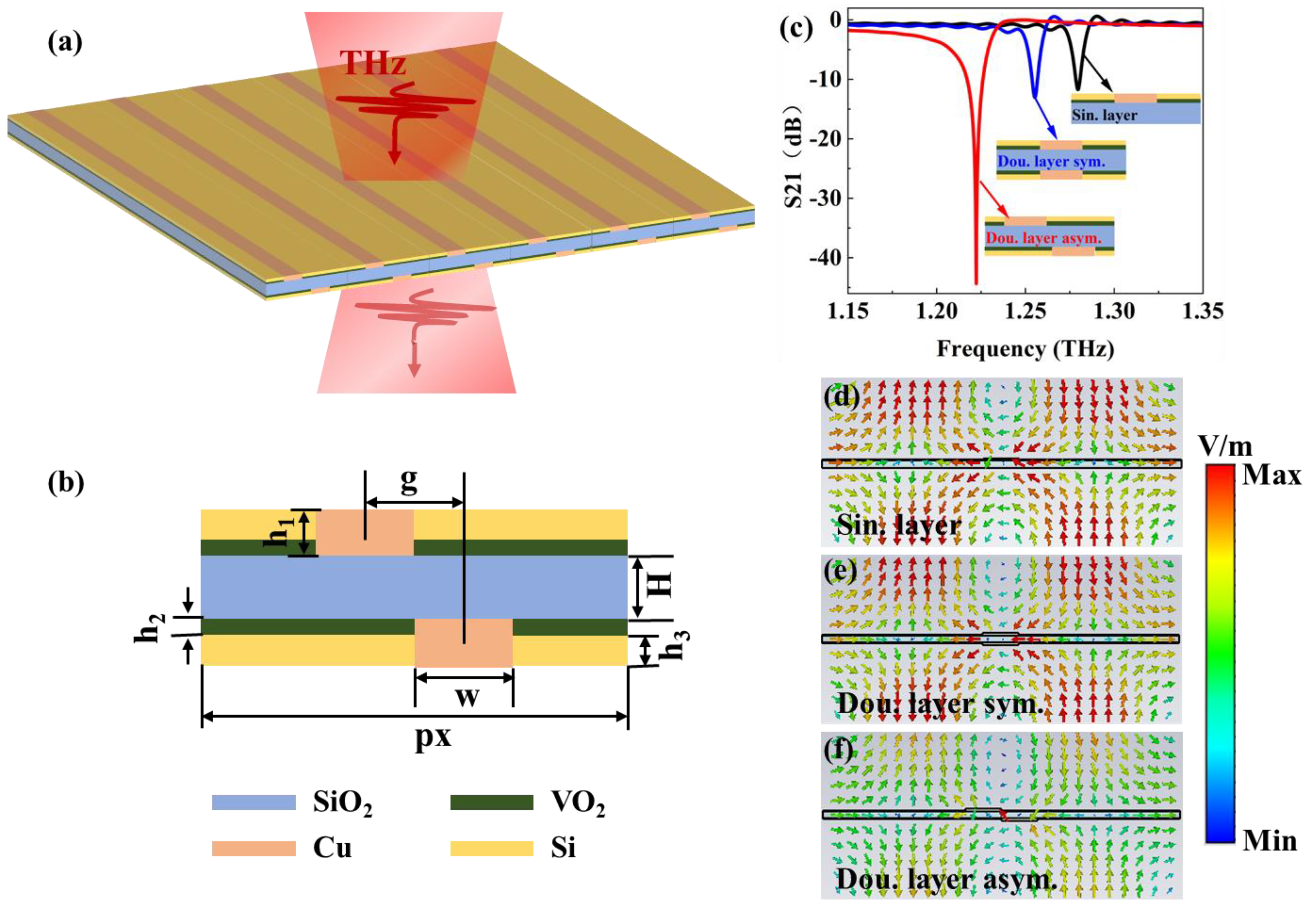
Figure 1 illustrates the structure of the THz metamaterial temperature sensor along with its electromagnetic spectral characteristics. As shown in
Figure 1(a), the unit structure consists of two identical copper strips and a VO₂ film, separated by a SiO₂ substrate, with a Si protective layer on the surface of the VO₂ film.
Figure 1(b) presents the front view of the unit structure, which includes two copper strips that function as a plasmonic superlattice. The symmetry breaking of the structure arises from the center-to-center distance (g) between the copper strips in the unit structure. The width of the copper strips is 30 µm, and their thickness is 2 µm. A 0.2 µm thick VO
2 film serves as the temperature-sensitive layer, regulating the transmittance of THz waves. The periodicity of the unit structure is maintained at (px=300) µm, which is chosen to provide the necessary momentum for the copper strips to excite waveguide modes through coherent plasmonic scattering in the THz frequency range. Consequently, for a fixed waveguide thickness of (H=6) µm, the frequency of the waveguide modes is determined by the period. The simulation results are obtained using the well-established 3D full-wave solver, which is based on the finite integral method. The x and y directions are set as magnetic and electric boundaries, respectively, while the z direction is an open boundary, allowing THz waves to propagate along the z-axis. Waveguide ports 1 and 2 are positioned on the negative and positive orientations of the z-axis, respectively, with an accuracy of -80 dB. The dielectric constant of SiO
2 is 3.9, while that of Si is 11.9. The conductivity of copper is 5.96×10
7 S/m.
3. Results and Discussion
As shown in
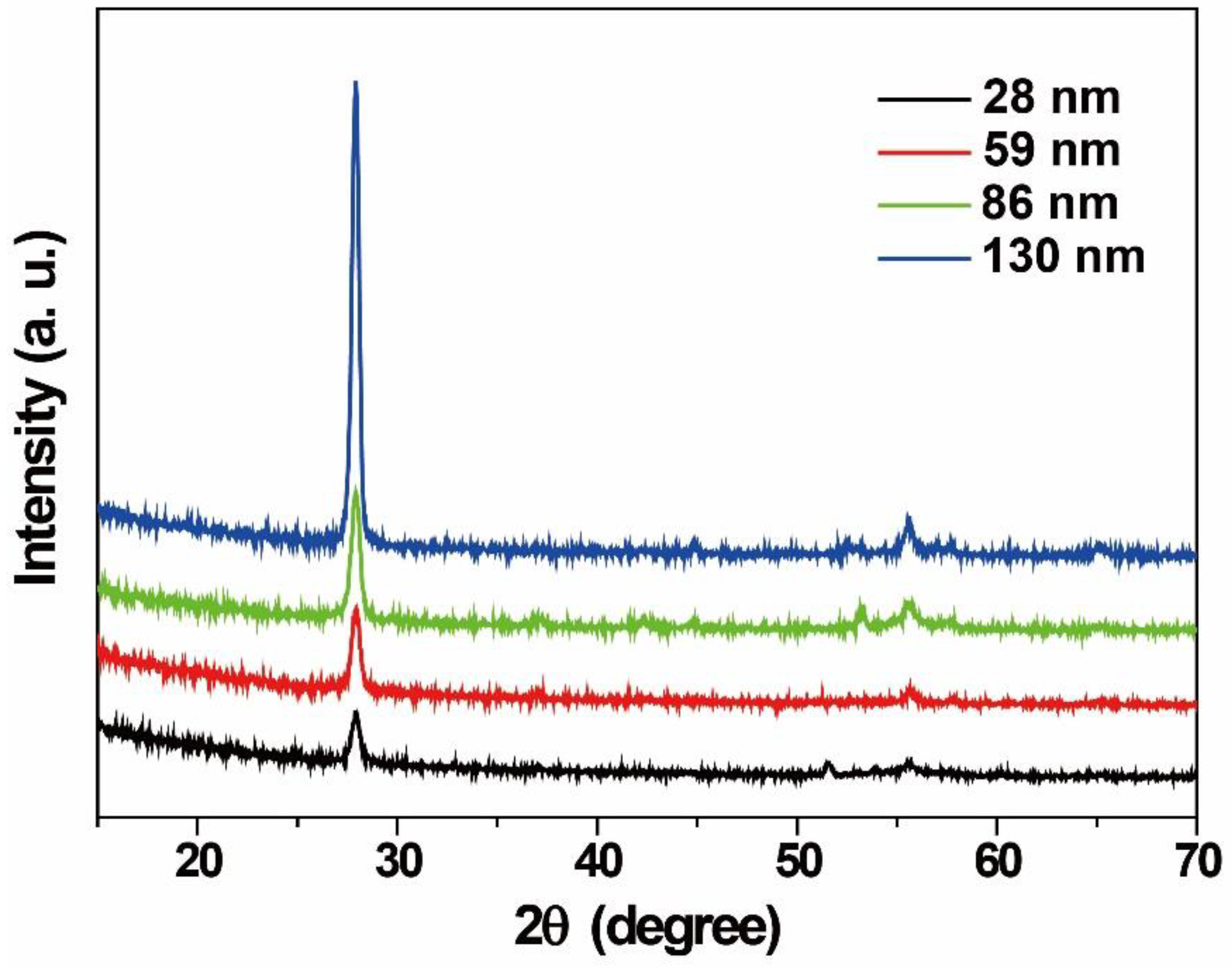
Figure 2, the films with thickness of 28 nm, 59 nm, 86 nm and 130 nm exhibit high-purified monoclinic VO2 phase (JCPDS card no. 72-0514). Although the films present polycrystalline characteristic, a strong diffraction peak at around 27.98° indicates that a (011) preferred growth orientation can be observed. The surface morphology of the films with different thicknesses were collected in
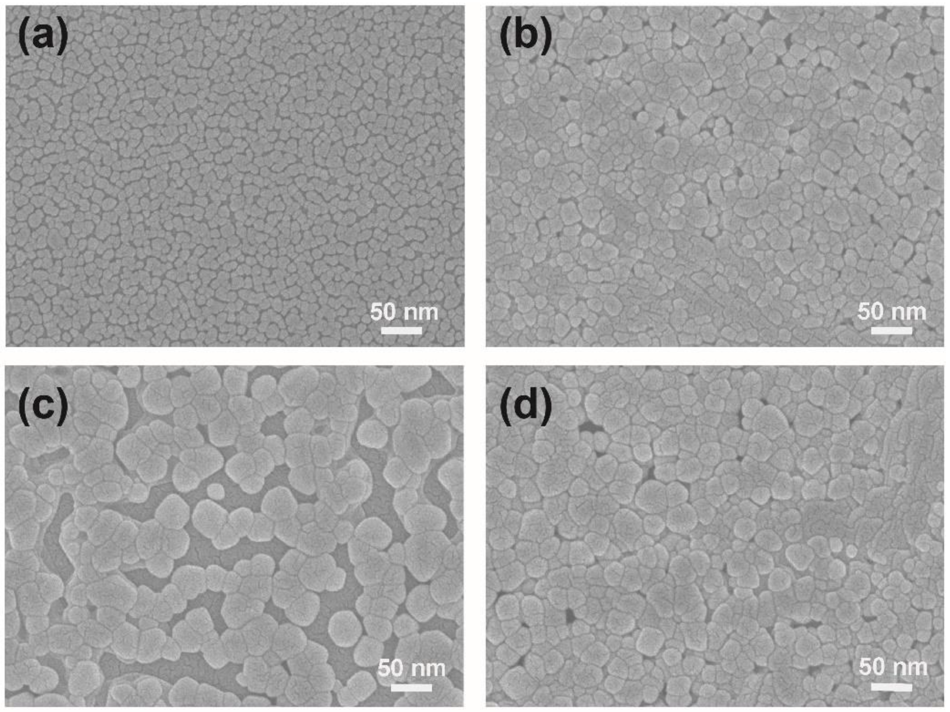
Figure 3. It shows that the film becomes more compact by increasing the thickness from 28 nm to 59 nm. But an obvious hybrid-growth mode can be observed when the film thickness increases further. It refers to an island-growth mode when the film thickness increases from 59 nm to 86 nm, but a layer-growth mode plays more important role when the film thickness increases from 86 nm to 130 nm. What is more important, by increasing the film thickness gradually, the VO
2 with compact morphology can be obtained. And the compact structure can lead to enhanced phase transition amplitude, as illustrated in previous report[
33].
Table 1 illustrates the resistivity of the films before (at room temperature) and after phase transition (at 85 ℃). It further confirms that the phase transition amplitude of the VO
2 film can be enhanced with compact morphology. And the film with thickness of 130 nm can reach around 3 orders of change in the resistivity across the phase transition.
Figure 1(c) compares the S21 parameters of the SLS, DLSS, and DLAS. For the SLS and DLSS, transmission dips occur at frequencies of 1.28 THz and 1.26 THz, with amplitudes of -11.72 dB and -13.12 dB, respectively. The amplitude of the transmission dip for the DLAS is -44.33 dB, with the resonance frequency red-shifting to 1.22 THz.
To further elucidate the formation mechanism of this transmission dip,
Figure 1(d) -(f) present the corresponding electric field distributions. The formation mechanisms of the transmission dips for the SLS, DLSS, and DLAS are similar. The interaction between the THz waves and the Cu strips excites plasmonic modes, which interact with transverse waveguide modes, leading to the formation of the transmission dips. Specifically, the transmission dip originates from the spectral overlap between the narrow transmission band of the waveguide mode and the broad plasmonic scattering band associated with the Cu strips. The narrow transmission band is generated by the scattering of localized plasmonic modes within the Cu strips, which excite the waveguide mode (i.e., the bright-dark mode). In contrast, the broad plasmonic band is directly excited by the localized plasmonic modes present in the Cu strips. Therefore, the spectral position and linewidth of the transmission dip are determined by the coupling strength between these two modes.
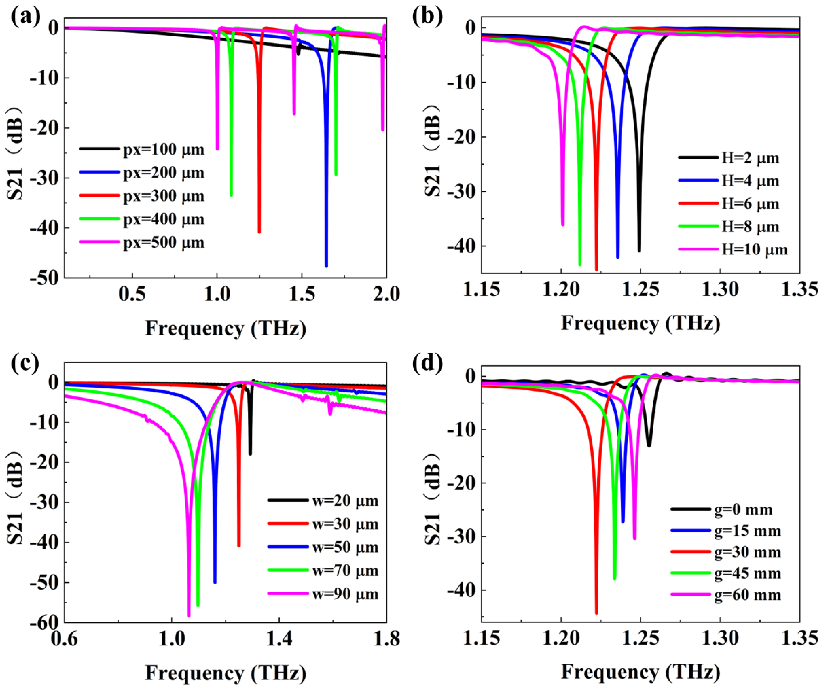
Figure 4 illustrates the optimization process of the parameters of the unit structure. The impact of the unit structure period on the transmission spectrum is shown in
Figure 4(a). When the unit structure period is 100 µm, it fails to provide sufficient momentum, preventing the Cu strips from exciting waveguide modes through coherent plasmonic scattering, which resulting in no resonance formation, as indicated by the black line in
Figure 4(a). As the unit structure period increases to 200 µm, there is enough momentum to form a transmission dip at a frequency 1.64 THz, with an amplitude of -47.87 dB. Further increasing the period causes the resonance frequency to shift to lower frequencies. For instance, at a unit structure period of 300 µm, the resonance frequency is 1.25 THz, with a corresponding amplitude of -40.97 dB. Continuing to increase the unit structure period excites additional resonances, as shown by the green and purple lines in
Figure 4(a).
The effect of the SiO2 substrate thickness on the transmission dip is depicted in
Figure 4(b). As the substrate thickness increases, the frequency of the transmission dip shifts to lower frequencies, while the amplitude first decreases and then increases. At substrate thicknesses of 2, 4, 6, 8, and 10 µm, the transmission dip frequencies are 1.25, 1.24, 1.22, 1.21, and 1.20 THz, with corresponding amplitudes of -40.97, -42.23, -44.33, -43.52, and -36.06 dB.
Figure 4(c) demonstrates the influence of the width of the Cu strips on the transmission spectrum. As the width of the Cu strips increases, the frequency of the transmission dip shifts to lower frequencies, the amplitude decreases, and the bandwidth increases. When the width of the Cu strips increases from 20 µm to 90 µm, the resonance frequency shifts from 1.29 THz to 1.06 THz, and the amplitude decreases from -18.21 dB to -58.69 dB.
Figure 4(d) illustrates the effect of the asymmetry of the unit structure on the transmission spectrum. As the asymmetry increases, the resonance frequency initially shifts to lower frequencies and then to higher frequencies. When the asymmetry increases from 0 µm to 30 µm, the resonance frequency shifts from 1.26 THz to 1.22 THz, with the amplitude decreasing from -13.15 dB to -44.33 dB. As the asymmetry continues to increase to 60 µm, the resonance frequency blue shifts to 1.25 THz, and the amplitude increases to -30.43 dB. This behavior occurs because, at higher asymmetry, the interaction between the two Cu strips gradually weakens, leading to a reduction in the ultimately excited resonance. This results in the blue shift of the transmission dip frequency and an increase in amplitude.
VO₂ is a material that exhibits a reversible insulator-metal phase transition, during which its conductivity experiences a dramatic change of 4-5 orders of magnitude. This characteristic makes it suitable as a sensitive layer for temperature sensors, enabling high-sensitivity temperature measurements by monitoring its phase transition properties.
Figure 5(a) shows the transmission spectrum of VO₂ films at different conductivities. As the conductivity of the VO₂ film increases from 10 S/m to 5000 S/m, there is no significant change in the resonance frequency of the transmission dip, while the amplitude gradually increases from -44.33 dB to -4.78 dB, achieving a modulation depth of up to 89%, as illustrated in
Figure 5(b).
Figure 5(c)-(f) present the electric field distribution maps at the resonance frequency for different conductivities. In low-temperature environments, the VO₂ film remains in the insulating phase with low conductivity. At this stage, the asymmetric Cu strips within the unit structure excite a plasmonic mode that interacts with the transverse waveguide mode, forming a very narrow transmission dip at a frequency of 1.29 THz. As the temperature rises to the phase transition temperature of the VO₂ film, its conductivity gradually increases. Consequently, the plasmonic mode excited by the asymmetric Cu strips weakens, leading to a reduced interaction with the transverse waveguide mode. This weakening of resonance results in an increase in the value of the transmission dip, indicating the sensor's sensitivity to temperature changes. Overall, the unique properties of VO₂, combined with its significant conductivity variation during the phase transition, make it an excellent candidate for high-performance temperature sensing applications.
4. Conclusions
This work proposes a phase transition oxide-based THz metamaterials for non-contact temperature sensor. The systematic structure is composed of two identical Cu strips and a VO₂ film separated by a SiO₂ substrate. This study examines the effects of various parameters, including the unit structure period, the thickness of the SiO₂ substrate, the width of the Cu strips, the degree of asymmetry, and the conductivity of the VO₂ film. The results indicate that the temperature-induced reversible phase transition of the VO₂ film alters its conductivity, thereby controlling the transmission of THz waves and facilitating environmental temperature monitoring. As the conductivity of the VO₂ film varies from 10 to 5000 S/m, the amplitude of the transmission dip changes from -44.33 dB to -4.78 dB, achieving a modulation depth of up to 89%. Therefore, the designed THz metamaterial functions as a highly sensitive wireless passive temperature sensor and thermal switch.
Author Contributions
Conceptualization, Yong Gong and Jing Leng; methodology, Li, Luo, Jing Leng; software, Jing Leng; validation, Yong Gong, and Qiwu Shi; investigation, Yong Gong, and Jing Leng; writing—original draft preparation, Yong Gong, and Jing Leng; writing—review and editing, Qiwu Shi; supervision, Qiwu Shi; project administration, Yong Gong, Li Luo; funding acquisition, Yong Gong, Li Luo. All authors have read and agreed to the published version of the manuscript.
Institutional Review Board Statement
Not applicable.
Informed Consent Statement
Not applicable.
Data Availability Statement
Not applicable.
Acknowledgments
The work was financially supported by Sichuan University-Luzhou strategic cooperation special fund project (No. 2022CDLZ-24).
Conflicts of Interest
The authors declare no conflflict of interest.
References
- Root, W.; Bechtold, T.; Pham, T. Textile-Integrated Thermocouples for Temperature Measurement. Materials 2020, 13, 626. [Google Scholar] [CrossRef] [PubMed]
- Zhang, Z.; Liu, Z.; Lei, J.; Chen, L.; Li, L.; Zhao, N.; Fang, X.; Ruan, Y.; Tian, B.; Zhao, L. Flexible thin film thermocouples: From structure, material, fabrication to application. iScience 2023, 26, 107303. [Google Scholar] [CrossRef]
- Bodić, M.Z.; Aleksić, S.O.; Rajs, V.M.; Damnjanović, M.S.; Kisić, M.G. Thermally Coupled NTC Chip Thermistors: Their Properties and Applications. Sensors 2024, 24, 3547. [Google Scholar] [CrossRef] [PubMed]
- Fang, Z.; Shen, C.; Qiu, T. Research progress of BaTiO3-system PTC thermistor materials. Electron. Compon. Mater. (China), 2010, 29, 69–71. [Google Scholar] [CrossRef]
- Chen, Z.-H.; Huang, P.-H.; Wang, C.-P.; Chih, Y.-D.; Lin, C.-J.; King, Y.-C. Embedded Near-Infrared Sensor With Tunable Sensitivity for Nanoscale CMOS Technologies. IEEE Sensors J. 2018, 19, 933–939. [Google Scholar] [CrossRef]
- Usamentiaga, R.; Venegas, P.; Guerediaga, J.; Vega, L.; Molleda, J.; Bulnes, F.G. Infrared Thermography for Temperature Measurement and Non-Destructive Testing. Sensors 2014, 14, 12305–12348. [Google Scholar] [CrossRef] [PubMed]
- Zhong, S. Progress in terahertz nondestructive testing: A review. Front. Mech. Eng. 2018, 14, 273–281. [Google Scholar] [CrossRef]
- A Hafez, H.; Chai, X.; Ibrahim, A.; Mondal, S.; Férachou, D.; Ropagnol, X.; Ozaki, T. Intense terahertz radiation and their applications. J. Opt. 2016, 18, 093004. [Google Scholar] [CrossRef]
- Xu, W.; Xie, L.; Ying, Y. Mechanisms and applications of terahertz metamaterial sensing: a review. Nanoscale 2017, 9, 13864–13878. [Google Scholar] [CrossRef]
- Ajayan, J.; Sreejith, S.; Manikandan, M.; Lai, W.-C.; Saha, S. Terahertz sensors for next generation biomedical and other industrial electronics applications: A critical review. Sensors Actuators A: Phys. 2024, 369. [Google Scholar] [CrossRef]
- Sizov, F. THz radiation sensors. Opto-Electronics Review, 2010, 18, 10–36. [Google Scholar] [CrossRef]
- Huang, Y.; Singh, R.; Xie, L.; Ying, Y. Attenuated Total Reflection for Terahertz Modulation, Sensing, Spectroscopy and Imaging Applications: A Review. Appl. Sci. 2020, 10, 4688. [Google Scholar] [CrossRef]
- Meinzer, N.; Barnes, W.L.; Hooper, I.R. Plasmonic meta-atoms and metasurfaces. Nature Photon- 2014, 8, 889–898. [Google Scholar] [CrossRef]
- Choi, M.; Lee, S.H.; Kim, Y.; Kang, S.B.; Shin, J.; Kwak, M.H.; Kang, K.-Y.; Lee, Y.-H.; Park, N.; Min, B. A terahertz metamaterial with unnaturally high refractive index. Nature 2011, 470, 369–373. [Google Scholar] [CrossRef]
- Liu, Y.; Zhang, X. Metamaterials: a new frontier of science and technology. Chem. Soc. Rev. 2011, 40, 2494–2507. [Google Scholar] [CrossRef]
- Schurig, D.; Mock, J.J.; Justice, B.J.; Cummer, S.A.; Pendry, J.B.; Starr, A.F.; Smith, D.R. Metamaterial Electromagnetic Cloak at Microwave Frequencies. Science 2006, 314, 977–980. [Google Scholar] [CrossRef]
- Beruete, M.; Jáuregui-López, I. Terahertz Sensing Based on Metasurfaces. Adv. Opt. Mater. 2019, 8, 1900721. [Google Scholar] [CrossRef]
- Kim, H.S.; Cha, S.H.; Roy, B.; Kim, S.; Ahn, Y.H. Humidity sensing using THz metamaterial with silk protein fibroin. Opt. Express 2018, 26, 33575–33581. [Google Scholar] [CrossRef]
- Degl’innocenti, R.; Lin, H.; Navarro-Cía, M. Recent progress in terahertz metamaterial modulators. Nanophotonics 2022, 11, 1485–1514. [Google Scholar] [CrossRef]
- Wang, W.; Sun, K.; Xue, Y.; Lin, J.; Fang, J.; Shi, S.; Zhang, S.; Shi, Y. A review of terahertz metamaterial sensors and their applications. Opt. Commun. 2024, 556. [Google Scholar] [CrossRef]
- Ma, L.; Shi, W.N.; Fan, F.; Zhang, Z.Y.; Zhang, T.R.; Liu, J.Y.; Wang, X.H.; Chang, S.J. Terahertz polarization sensing, chirality enhancement, and specific binding based on metasurface sensors for biochemical detection: a review Invited. Chin. Opt. Lett. 2023, 21, 18. [Google Scholar] [CrossRef]
- Shen, S.; Liu, X.; Shen, Y.; Qu, J.; Pickwell-MacPherson, E.; Wei, X.; Sun, Y. Recent Advances in the Development of Materials for Terahertz Metamaterial Sensing. Adv. Opt. Mater. 2021, 10, 2101008. [Google Scholar] [CrossRef]
- Li, W.; Cheng, Y. Dual-band tunable terahertz perfect metamaterial absorber based on strontium titanate (STO) resonator structure. Opt. Commun. 2020, 462, 125265. [Google Scholar] [CrossRef]
- Li, D.; Huang, H.; Xia, H.; Zeng, J.; Li, H.; Xie, D. Temperature-dependent tunable terahertz metamaterial absorber for the application of light modulator. Results Phys. 2018, 11, 659–664. [Google Scholar] [CrossRef]
- Sheta, E.; Choudhury, P.; Ibrahim, A.-B.M. “Pixelated graphene-strontium titanate metamaterial supported tunable dual-band temperature sensor” Opt. Mater. 117, 111197 (2021). Opt. Mater. 2021, 118, 111225. [Google Scholar] [CrossRef]
- Keshavarz, A.; Zakery, A. Ultrahigh sensitive temperature sensor based on graphene-semiconductor metamaterial. Appl. Phys. A 2017, 123, 797. [Google Scholar] [CrossRef]
- Luo, H.; Wang, X.; Qian, H. Tunable terahertz dual-band perfect absorber based on the combined InSb resonator structures for temperature sensing. J. Opt. Soc. Am. B 2021, 38, 2638–2644. [Google Scholar] [CrossRef]
- Rong, C.; Cai, B.; Cheng, Y.; Chen, F.; Luo, H.; Li, X. Dual-band terahertz chiral metasurface absorber with enhanced circular dichroism based on temperature-tunable InSb for sensing applications. Phys. Chem. Chem. Phys. 2024, 26, 5579–5588. [Google Scholar] [CrossRef]
- Wang, Y.; Qiu, Y.; Zhang, Y.; Lang, T.; Zhu, F. High-Sensitivity Temperature Sensor Based on the Perfect Metamaterial Absorber in the Terahertz Band. Photonics 2023, 10, 92. [Google Scholar] [CrossRef]
- Morin, F.J. Oxides Which Show a Metal-to-Insulator Transition at the Neel Temperature. Phys. Rev. Lett. 1959, 3, 34–36. [Google Scholar] [CrossRef]
- Chang, X.; Li, J.; Mu, J.; Ma, C.-H.; Huang, W.; Zhu, H.-F.; Liu, Q.; Du, L.-H.; Zhong, S.-C.; Zhai, Z.-H.; et al. Impact of the uniaxial strain on terahertz modulation characteristics in flexible epitaxial VO2 film across the phase transition. Opt. Express 2023, 31, 13243–13254. [Google Scholar] [CrossRef] [PubMed]
- Li, M.; Magdassi, S.; Gao, Y.; Long, Y. Hydrothermal Synthesis of VO2 Polymorphs: Advantages, Challenges and Prospects for the Application of Energy Efficient Smart Windows. Small 2017, 13. [Google Scholar] [CrossRef] [PubMed]
- Shi, Q.; Huang, W.; Lu, T.; Zhang, Y.; Yue, F.; Qiao, S.; Xiao, Y. Nanostructured VO2 film with high transparency and enhanced switching ratio in THz range. Appl. Phys. Lett. 2014, 104, 071903. [Google Scholar] [CrossRef]
|
Disclaimer/Publisher’s Note: The statements, opinions and data contained in all publications are solely those of the individual author(s) and contributor(s) and not of MDPI and/or the editor(s). MDPI and/or the editor(s) disclaim responsibility for any injury to people or property resulting from any ideas, methods, instructions or products referred to in the content. |
© 2024 by the authors. Licensee MDPI, Basel, Switzerland. This article is an open access article distributed under the terms and conditions of the Creative Commons Attribution (CC BY) license (http://creativecommons.org/licenses/by/4.0/).


