1. Introduction
Recently, crystallography has been using an increasingly sophisticated mathematical apparatus [
1,
2,
3,
4,
5,
6,
7] to decipher structures whose reliable identification was impossible in the recent past. At the same time, researchers-technologists who use X-ray structural analysis to trace structural changes during technological manipulations live in a different world and use the Wolf-Bragg and Scherrer formulae to study the resulting structures. But even with this approach, by carefully analysing the diffractograms obtained, it is possible to find something that no one has encountered so far.
A striking example of this is the experiment described in Nature Electronics [
8]. The discovery was made by accident during the study of phase transitions in vanadium dioxide (VO
2). VO
2 has an insulating phase at room temperature and abruptly transforms into a metal at 68°C when its lattice structure changes. Classically, VO
2 has an energy-dependent memory: ‘the material returns to the insulating state as soon as the excited state stops,’ says Mohammad Samizadeh Nikoo, a PhD student in the POWERlab at École Polytechnique Fédérale de Lausanne who discovered the property. In his thesis, he intended to find out how long it takes for VO
2 to transition from one state to another. But his research led him down a different path: after hundreds of measurements, he discovered a ‘memory effect’ in the structure of the material.
In his experiments, the scientist applied an electric current to a sample of VO2. The current moved through the material, following a path until it exited, on the other side. As the current heated the sample, the VO2's states changed. And as soon as the current passed, the material returned to its original state. A second pulse of current was then passed through the material. It turned out that the time it took for the material to change state was directly related to its history: VO2 seemed to ‘remember’ the first phase transition and anticipate the next one.
In our studies, we also stumbled upon the ‘structure memory effect’. When removing lead from the solution of tungsten in lead by vacuum annealing at Т = 800 oС , tungsten atoms remain in the places where they were in the solid solution of tungsten in lead, although lead in the sample in accordance with the conditions of heat treatment does not remain at all. To increase the reliability of the studies, we tried to combine X-ray diffraction studies with complementary studies using a scanning electron microscope.
2. Experimental details
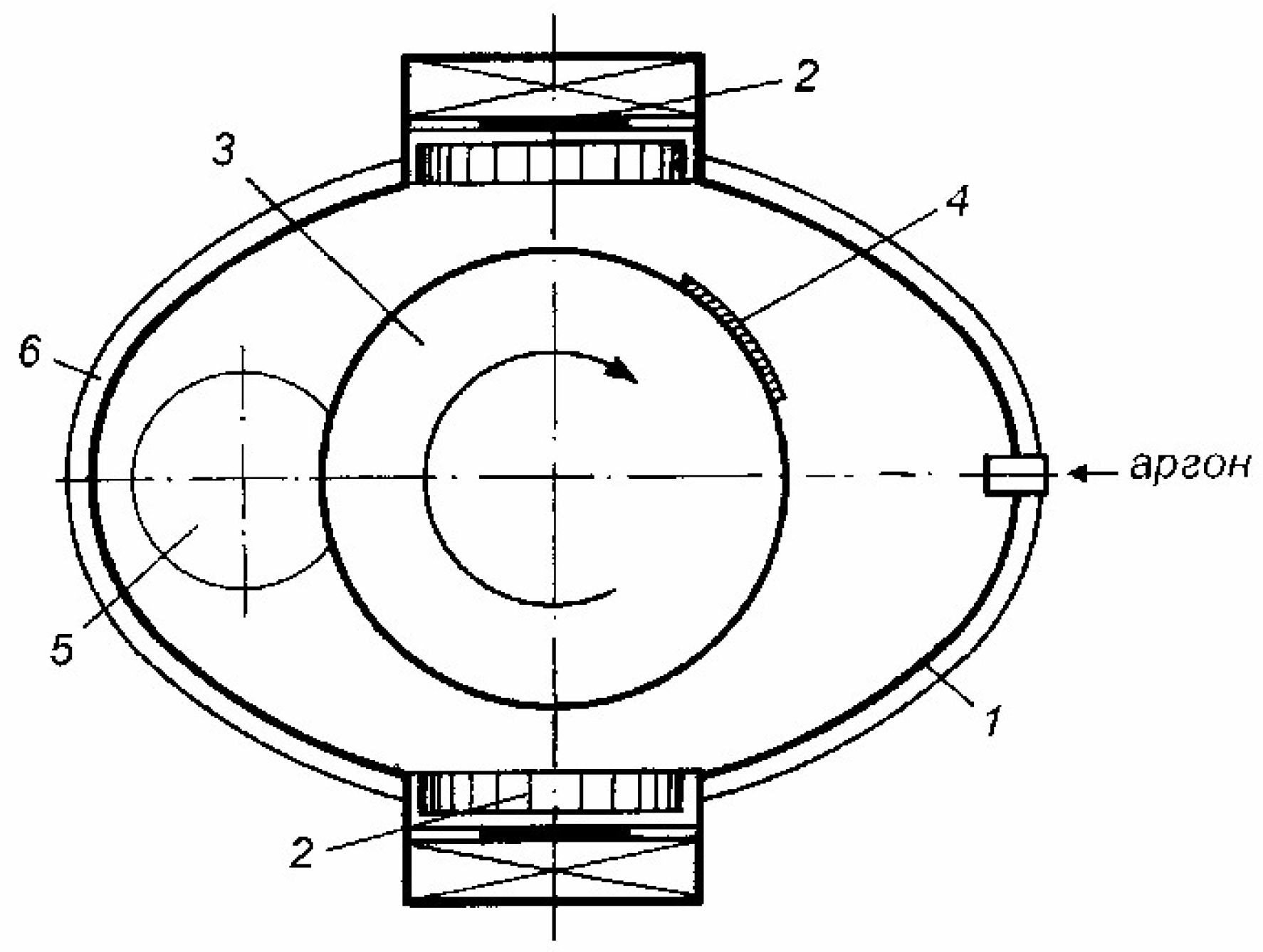
Ion-plasma unit. For the preparation of samples of coatings of the tungsten-lead system, an ion-plasma unit with two independent magnetron sputtering systems was developed, the scheme of which is shown in
Figure 1.
The unit is a vacuum chamber, on the walls of which planar DC magnetrons are placed. At the same time atomised targets are cathodes, behind which water-cooled magnetic systems are located. Inside the vacuum chamber mounted cylinder with the ability to rotate around the axis to mount substrates and move them relative to the magnetrons. For the preparation of samples of coatings of the tungsten-lead system selected rotation speed of 10 revolutions per minute. Thus, for the time of sputtering, which for coatings of this system was 40-60 minutes, each substrate passed by sputtering tungsten and lead magnetrons 400-600 times. The experimental setup is described in more detail in [
9,
10].
Sample preparation included sequential operations of simultaneous sputtering of tungsten and lead targets in low-pressure plasma and deposition of sputtered materials on unheated substrates moving relative to plasma flows in the form of island films - layers of nanometre thickness. The thicknesses of the layers were determined by calculating the mass change of tungsten and lead targets during the sputtering time measured using microanalytical scales.
The temperature of substrates during the formation of samples did not exceed 100 oС. In experiments tungsten 99.96 mas. % of the basic element and lead (99.99 mass. %) in the form of targets with diameter 40 and thickness 4 mm.
The ratio of metal concentrations in the samples was changed by atomisation rate of targets of planar magnetron atomisers. In the process of atomisation of targets the power was kept constant at each of the atomising devices. The ratio of deposited components was controlled by weight method - by the amount of sputtered and deposited metal during the formation of the coating and, in parallel, by the method of Reserford backscattering of ions N14 on the accelerator DC-60 Eurasian University (Nur-Sultan, Kazakhstan).
X-ray diffraction (XRD) measurements were performed on a Bruker D8 ‘Discover’ X-ray diffractometer. The X-ray beam exiting the copper target was collimated by a parabolic multilayer mirror and a reflective monochromator made of pyrolytic graphite tuned to emit Kα -radiation of Cu. The imaging was performed in Bagg-Brentano geometry (Θ-2Θ) in the angle range 2Θ=20-90o with a step of 0.01o.
Electron microscopic studies were performed with an electron probe microanalyser JSM-8230 (JEOL).
High-temperature annealings were carried out on a vacuum high-temperature furnace based on the URVT -2500 unit.
3. Results and Discussion
This section may be divided by subheadings. It should provide a concise and precise description of the experimental results, their interpretation, as well as the experimental conclusions that can be drawn.
Using the setup shown in
Figure 1, coatings were sputtered onto polycor (α-Al
2O
3) substrates of three different compositions, details of which are presented in
Table 1.
The obtained coatings were annealed in oil-free vacuum at 800 oС for 1 hour and 6 hours, after which the annealed and non-annealed samples were diffractometrically investigated on a Bruker D8 Advance diffractometer, the results of which are given below.
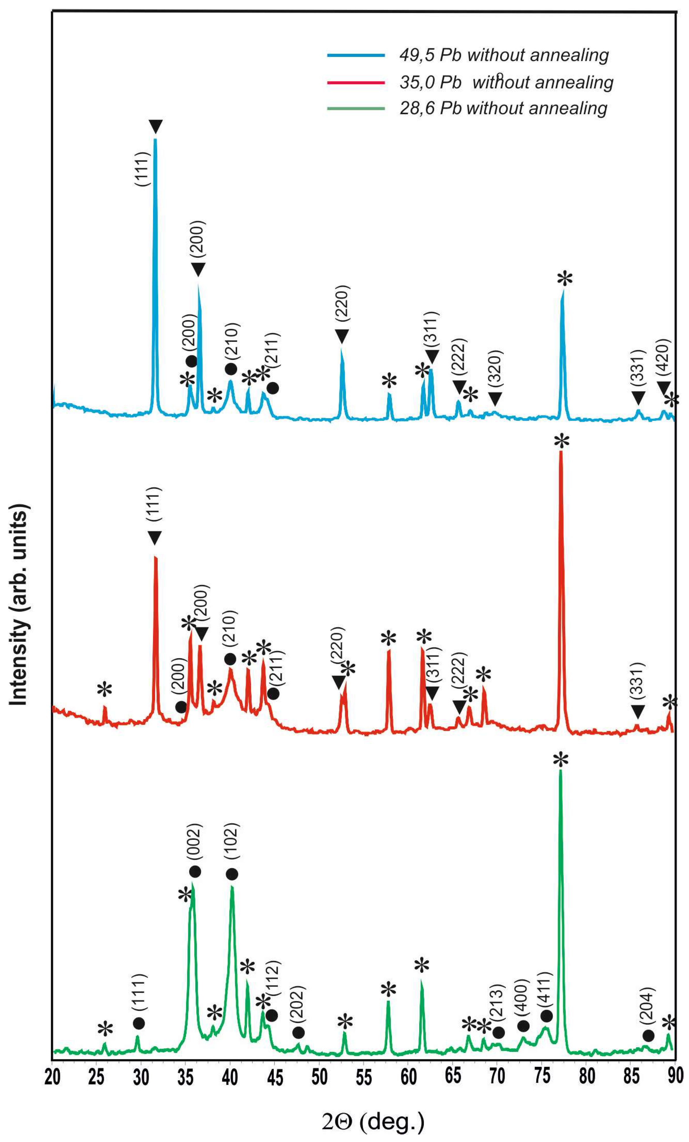
Figure 2 shows the diffractograms of unannealed coatings of the W-Pb system with lead content of 28.6, 35.0 and 49.5 at.%. From comparison of the diffractograms it can be seen that at the concentration of 28.6 at.% lead is completely dissolved in β-W. The cubic lattice of β-W undergoes tetragonal distortion and the calculated lattice parameters are a = 0.5220 nm and c = 0.5012 nm. When the lead content in the coating increases to 35.0 at.%, it begins to crystallise as a separate phase with tabulated lattice parameters. The phase of lead solution in β-W becomes finely crystalline and is well enough described in cubic syngony, lattice parameter at that a = 0.5077±0.0011 nm. At further increase of lead concentration in the coating up to 49.5at.% the ratio between pure lead and lead solution in β-W shifts even more strongly in favour of lead, lead solution in β-W has cubic lattice A15 with parameter a = 0.5063±0.0005 nm.
To test the possibility of obtaining porous structures from tungsten, coatings of the W-Pb system both completely consisting of solid solution of Pb in W (28.6 at.% Pb) and with excess of lead and with excess of lead (35.0 and 49.5 at.% Pb) were annealed in vacuum at Т = 800oС. The annealing temperature was chosen obviously higher than the boiling point of lead in order to achieve complete evaporation of lead during annealing.
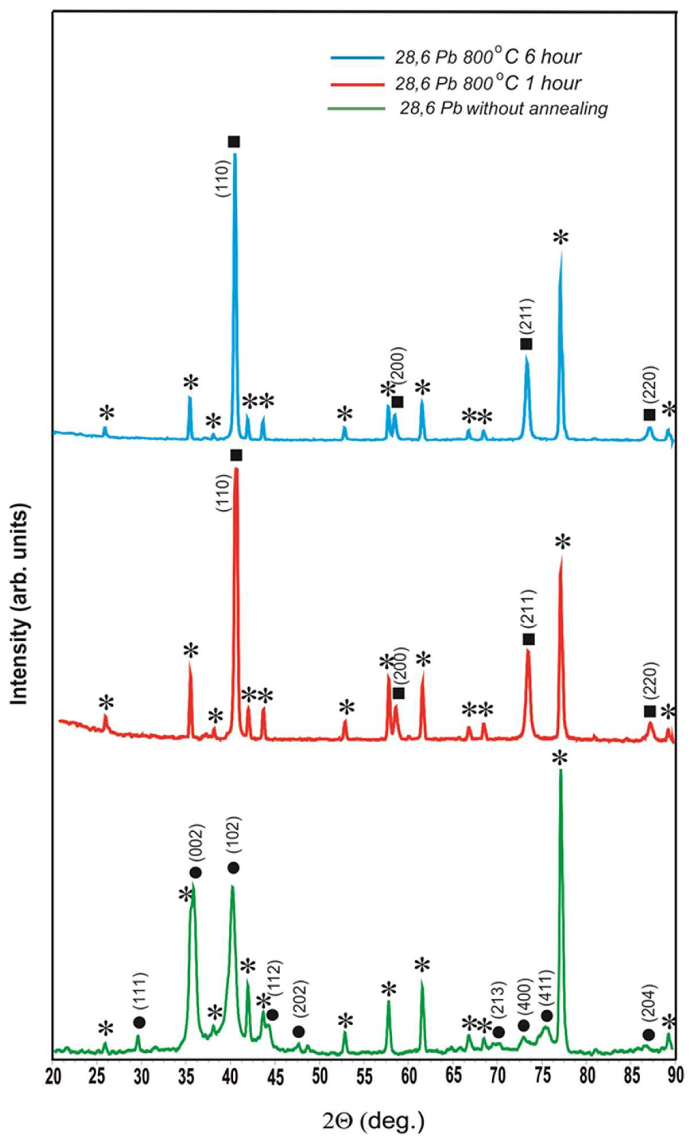
Figure 3 shows the diffractograms of the coating with lead content 28.6 at.% without annealing and after annealing at 800
oС for 1 hour and 6 hours.
As can be seen from
Figure 3, as a result of annealing 800
oС 1 h, the solid solution of lead in β-W completely transformed into α-W with lattice parameter a = 0.3163 ± 0.0002 nm. After annealing 800
oС 6 hours, the X-ray diffraction pattern completely coincides with the X-ray diffraction pattern after annealing 800
oС 1 hour. So, according to the data of X-ray radiography , lead is completely evaporated from the coating with thickness of 2.6 μm in vacuum at T = 800
oС for 1 hour.
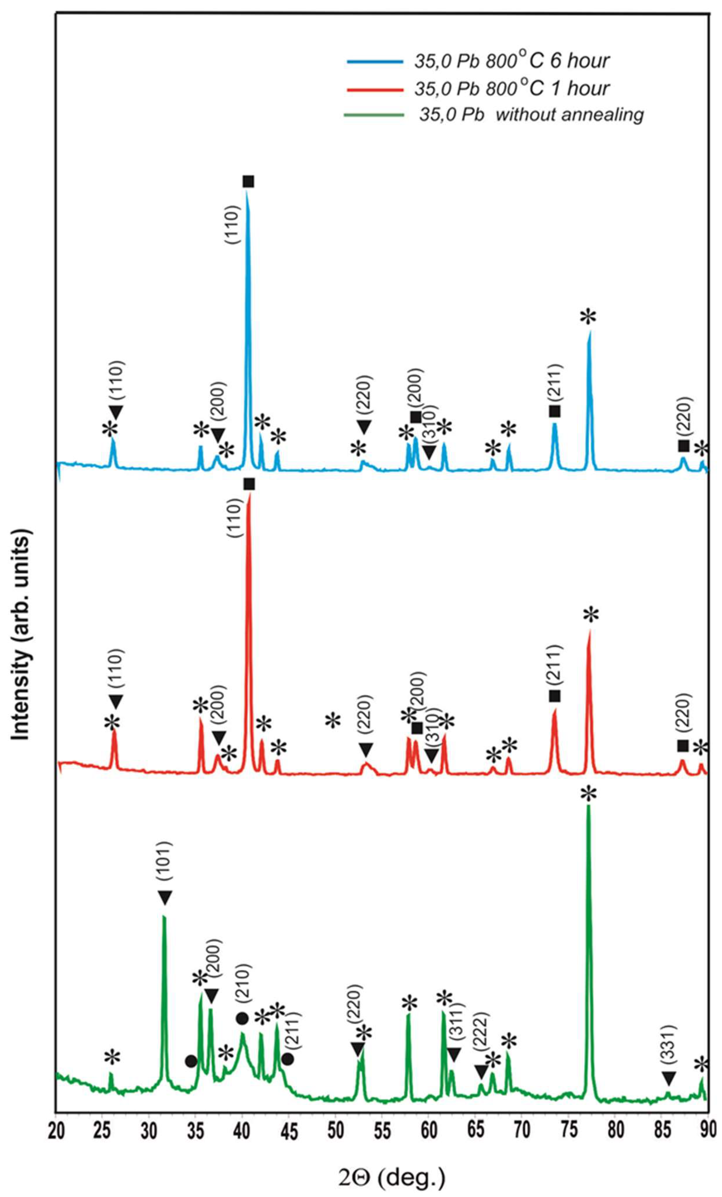
Figure 4.
Diffractograms of the coating with 35.0 at.% lead content without annealing and after 800 oС annealings of 1 h and 6 h, where ⁎ - polycor (α-Al2O3), ● - solid solution of Pb in β-W (a = 0.5077±0.0011 nm), ■ - α-W (a = 0.3163 ± 0.0002 nm), ▼ - oc-phase a = 0.4876±0.0009 nm.
Figure 4.
Diffractograms of the coating with 35.0 at.% lead content without annealing and after 800 oС annealings of 1 h and 6 h, where ⁎ - polycor (α-Al2O3), ● - solid solution of Pb in β-W (a = 0.5077±0.0011 nm), ■ - α-W (a = 0.3163 ± 0.0002 nm), ▼ - oc-phase a = 0.4876±0.0009 nm.
Analysis of the diffractograms after annealing at 800
oС for 1 h and 6 h shows that in addition to the peaks from α-W with the tabulated lattice parameter and polycore, there is a system of peaks with
dhkl, presented in
Table 2.
It can be seen that if the Miller indices in the second row of the table are assigned to the observed dhkl, it turns out that we observe an oocl lattice with the parameter a = 0.4878±0.0005 nm. The coincidence of diffractograms after annealing at 800 oС for 1 hour and 6 hours shows that the obtained phase is stable in time.
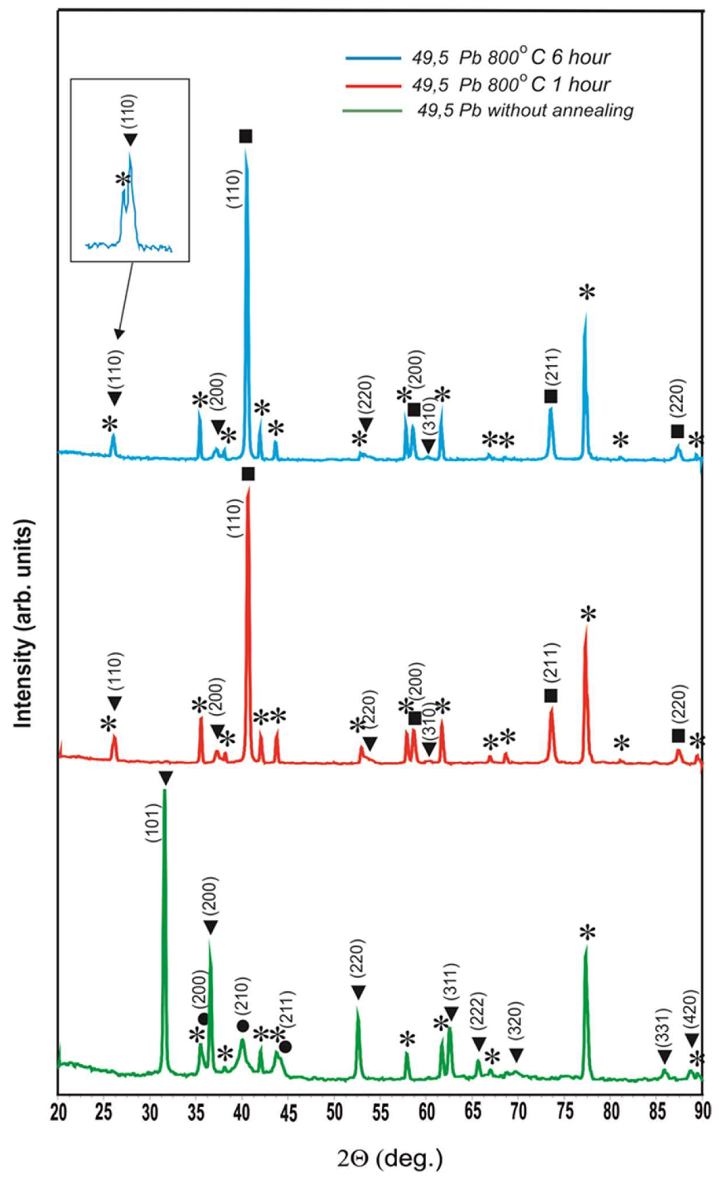
Figure 5 shows the diffractograms of the unannealed coating containing 49.5 at.% Pb and the same coating after annealing at 800
oС for 1 hour and 6 hours.
The diffractograms of this coating after 800
oС annealing for 1 hour and 6 hours completely coincide with the diffractograms of the coating with Pb content of 35.0 at.%. Therefore, it can be concluded that the existence of the occ phase with a = 0.4878±0.0005 nm after 800
oС annealing is a general pattern for coatings in which lead existed as a separate phase before annealing. In
Figure 4, a special insert is made on an enlarged scale so that no one doubts the reality of the existence of peak (110) of this phase. Moreover, it is necessary to note the fact that the lattice parameter of the detected phase a = 0.4878±0.0005 nm is only slightly less than the lattice parameter of lead (a
Pb = 0.4950 nm). The reasons for the occurrence of this phase, in our opinion, are as follows: during sputtering of coatings of the tungsten-lead system at a concentration of lead less than 28.6 at.% the formation of a solid solution of lead in β-W occurs. Above this threshold, some of the lead crystallises into a separate phase. A minor part of this lead dissolves tungsten as a result of nanoscale alloying and forms a solid solution of tungsten in lead. On the diffractograms of
Figure 1 the fact of existence of solid solution of tungsten in lead cannot be fixed due to the fact that a weak reflex from solid solution of tungsten in lead exists in the form of a weak distortion on the right part of peaks from pure lead. When heated at 800
oС in a vacuum, all of the lead - free, dissolved in β-W and dissolved tungsten - is vaporised. Where there was free lead, cavities remain. Lead from β-W evaporates with decrease of volume of the latter and cracks are formed in β-W as in clay when it dries in the sun. If lead dissolved in tungsten evaporates, then tungsten atoms remain in those places of the lattice, where they were in solid solution, and therefore a = 0.4878±0.0005 nm, but in the absence of a force field of lead atoms, the character of interaction of tungsten atoms among themselves changes and on the diffractogram we observe the occ lattice. Thus, the fact of tungsten dissolution in lead and the ability of atoms of the dissolved substance to memorise their position in the solvent lattice when the solvent atoms are removed from it are fixed.
To verify the above assumptions, electron microscopic studies were carried out on an electron probe microanalyser JSM-8230 (JEOL).
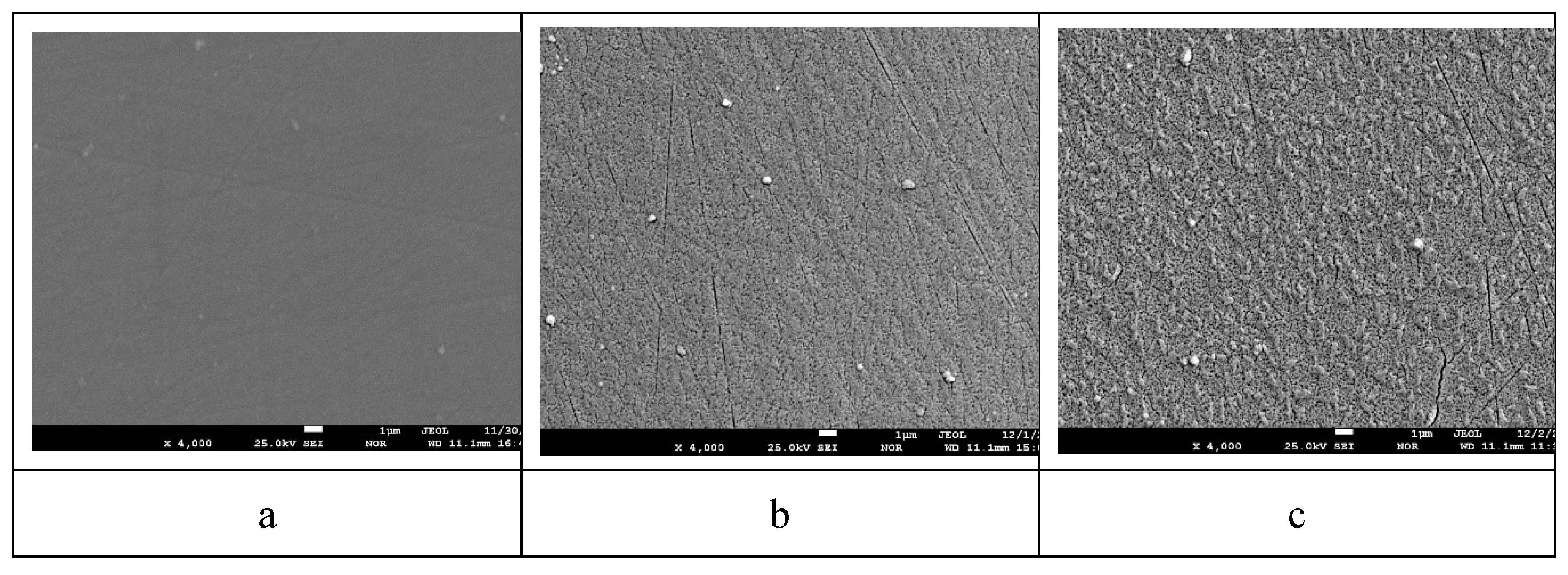
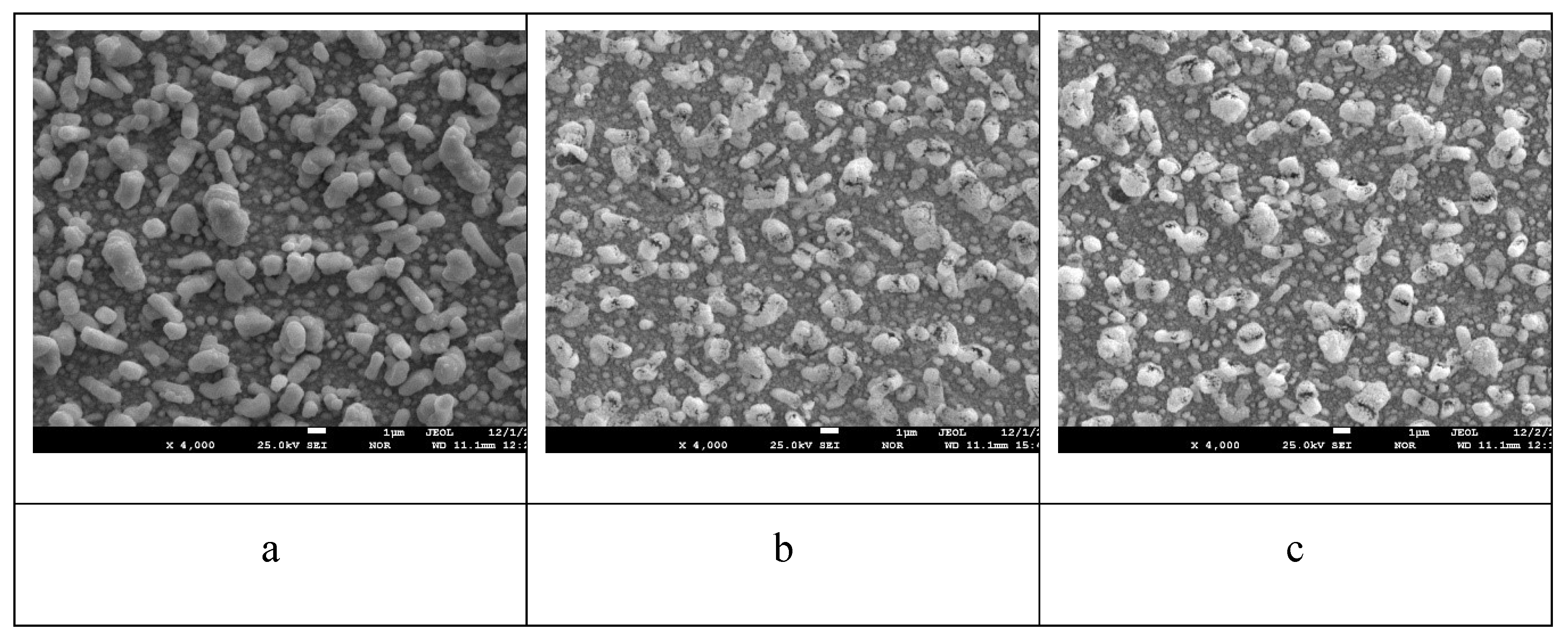
Figure 6 shows electron microscopic images of the surface of the sample with lead content 28.6 at.% before annealing and after annealing at 800 oC for 1 hour and 6 hours.
From the analysis of
Figure 6 shows that before annealing the surface of the coating was flat without any features. Even the stripes left on the surface of the polycor after polishing can be seen. After annealing 800
oС 1 hour (
Figure 6 (b)), many small pores and cracks on the coating surface can be seen. After annealing 800
oС 6 h (
Figure 6 (c)), it can be seen that the surface roughness due to the reduction of the coating volume has increased, as well as the number of pores and the size of the cracks covering the surface have increased.
Table 3 shows the results of EDS mapping of the sample with lead content of 28.6 at.% after annealing at 800
oС for 6 h (c).
From the EDS mapping results, it can be seen that lead completely evaporates from the coating after annealing at 800 oС for 6 hours. Obviously, the elements Al, O and C are related to the substrate (polycor), and tungsten is completely free of lead.
Figure 7 shows electron microscopic images of the surface of the sample with lead content of 35.0 at.% before annealing and after annealing at 800
oС for 1 hour and 6 hours.
From the analysis of
Figure 7, it can be seen that the coating surface after sputtering before annealing is dense and smooth, and numerous lead whiskers long enough stick out of it. After annealing 800
oС 1 hour (
Figure 7 (b)), it can be seen that there are many small pores and cracks in the coating surface, and holes have formed in the whisker walls and it can be seen that the whiskers are empty inside. After annealing 800
oС 6 h (Fig 6 (c)), it can be seen that the porosity of the coating between the whiskers has increased while the whisker shells remain unchanged. To understand the nature of the whiskers remaining after annealing 800
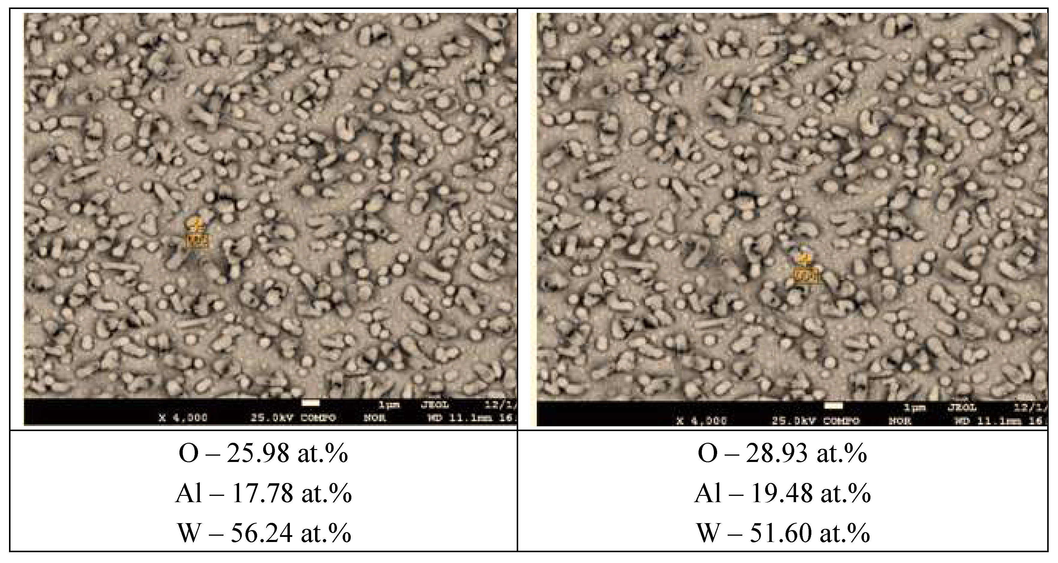
oС 6 h, let us consider the data from the spot EDS analysis at different points on the surface.
Figure 8 shows images of the 35.0 at.% coating surface with the elemental composition at these points.
It is evident that aluminium and oxygen refer to the substrate consisting of α-Al2O3. Since even when pointing directly at the surface of the whisker the instrument does not detect the presence of lead, it can be concluded that the outer surface of the whisker is formed by a solid solution of tungsten in lead, and it is the tungsten crust that remains after the lead has been evaporated. From the analysis of this image it can be seen that the average diameter of the lead whiskers is approximately 500-600 nm, and the wall thickness of these whiskers, which can be estimated from the analysis of the exposed whiskers, is 20-30 nm. To estimate the size of crystallites forming the walls of the phase whiskers, we used the Scherrer formula , where d is the average size of crystallites, K is the dimensionless particle shape factor (Scherrer constant), λ is the wavelength of X-ray radiation, β is the width of the reflex at half-height (in radians), Θ is the diffraction angle (Bragg angle). The programme Eva-2 from the Bruker D8 Advance diffractometer software package gives for the peak (200) of the X-ray diagram of 49.5 at.% Pb 800 oС 6 hours (Figure5 upper spectrum) the crystallite size equal to 24.9 nm.
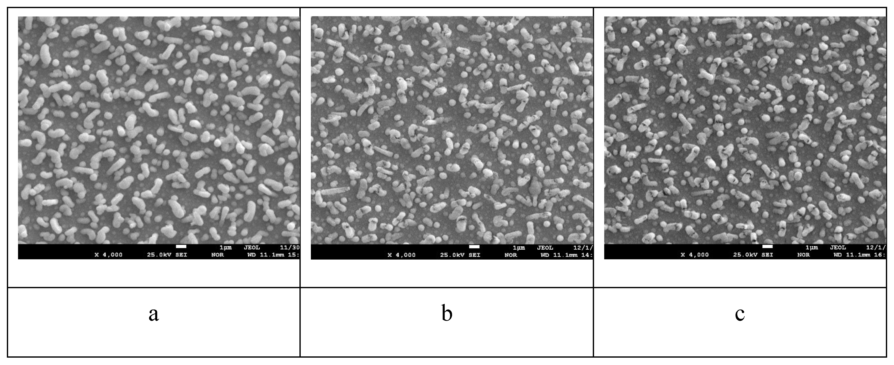
Figure 9 shows electron microscopic images of the surface of the sample with a lead content of 49.5 at.% before annealing and after annealing at 800
oС for 1 hour and 6 hours.
From the analysis of
Figure 9, it can be seen that the number of lead whiskers per unit surface has increased and the whiskers themselves have become thicker. After annealing 800
oС 1 hour (
Figure 7 (b)), it can be seen that there are many small pores on the coating surface, and holes have formed in the whisker walls and it can be seen that the whiskers are empty inside. After annealing 800
oС 6 h (
Figure 6 (c)), it can be seen that the porosity of the coating between the whiskers increased while the whisker shells remained unchanged. It is quite obvious that the porosity of the coating with initial lead concentration of 49.5 at.% after annealing 800
oС 6 h is maximum.
Thus, the possibility of obtaining porous tungsten coatings at vacuum annealing of 800 oС coatings of W-Pb system with lead content of 28.6, 35.0 and 49.5 at.% has been shown, and the character of porosity changes, and if the coating with 28.6 at.% is characterised by deep cracks in the surface and multiple point pores, then for the coating with 49.5 at.% the character of the surface becomes spongy.
In addition, the formation of a new tungsten phase during lead evaporation from a solid solution of tungsten in lead forming the outer walls of lead whiskers growing on the surface of sputtered coatings has been recorded.
Figure 1.
Schematic diagram of the installation for the formation of coatings of the tungsten-lead system: 1 - body of the vacuum chamber; 2-magnetrons; 3-cylinder; 4-substrate; 5-window for evacuation of gases; 6- caisson.
Figure 1.
Schematic diagram of the installation for the formation of coatings of the tungsten-lead system: 1 - body of the vacuum chamber; 2-magnetrons; 3-cylinder; 4-substrate; 5-window for evacuation of gases; 6- caisson.
Figure 2.
Diffractograms of non-annealed coatings of W-Pb system with different lead content: ⁎ - polycor (α-Al2O3), ● - solid solution of lead in β-W, ▼ - lead.
Figure 2.
Diffractograms of non-annealed coatings of W-Pb system with different lead content: ⁎ - polycor (α-Al2O3), ● - solid solution of lead in β-W, ▼ - lead.
Figure 3.
Diffractograms of the coating with 28.6 at.% lead content without annealing and after 800 oС annealings of 1 h and 6 h, where ⁎ is polycor (α-Al2O3), ● is solid solution of Pb in β-W (a = 0.5220 nm, c = 0.5012 nm), ■ is α-W (a = 0.3163 ± 0.0002 nm).
Figure 3.
Diffractograms of the coating with 28.6 at.% lead content without annealing and after 800 oС annealings of 1 h and 6 h, where ⁎ is polycor (α-Al2O3), ● is solid solution of Pb in β-W (a = 0.5220 nm, c = 0.5012 nm), ■ is α-W (a = 0.3163 ± 0.0002 nm).
Figure 5.
Diffractograms of the coating with lead content of 49.5at.% without annealing and after annealing at 800 oC for 1 h and 6 h, where ⁎ - polycor (α-Al2O3), ● - solid solution of Pb in β-W (a = 0.5077±0.0011 nm), ■ - α-W (a = 0.3163 ± 0.0002 nm), ▼ - oc-phase a = 0.4878±0.0005 nm.
Figure 5.
Diffractograms of the coating with lead content of 49.5at.% without annealing and after annealing at 800 oC for 1 h and 6 h, where ⁎ - polycor (α-Al2O3), ● - solid solution of Pb in β-W (a = 0.5077±0.0011 nm), ■ - α-W (a = 0.3163 ± 0.0002 nm), ▼ - oc-phase a = 0.4878±0.0005 nm.
Figure 6.
Electron microscopic images of the surface of the sample with lead content of 28.6 at.% before annealing (a) and after annealing at 800 oС for 1 hour (b) and 6 hours (c).
Figure 6.
Electron microscopic images of the surface of the sample with lead content of 28.6 at.% before annealing (a) and after annealing at 800 oС for 1 hour (b) and 6 hours (c).
Figure 7.
Electron microscopic images of the surface of the sample with lead content of 35.0 at.% before annealing (a) and after annealing at 800 oC for 1 hour (b) and 6 hours (c).
Figure 7.
Electron microscopic images of the surface of the sample with lead content of 35.0 at.% before annealing (a) and after annealing at 800 oC for 1 hour (b) and 6 hours (c).
Figure 8.
EDS analysis data at different points of the coating surface with 35.0 at.% Pb content.
Figure 8.
EDS analysis data at different points of the coating surface with 35.0 at.% Pb content.
Figure 9.
Electron microscopic images of the surface of the sample with lead content 49.5 at.% before annealing (a) and after annealing at 800 oС for 1 hour (b) and 6 hours (c).
Figure 9.
Electron microscopic images of the surface of the sample with lead content 49.5 at.% before annealing (a) and after annealing at 800 oС for 1 hour (b) and 6 hours (c).
Table 1.
The PW and PPb powers used in tungsten and lead sputtering, the recorded molar removal from each target nW and nPb, the thicknesses of the tungsten and lead partial layers dW dPb, the total coating thickness d, and the calculated lead concentration in the CPb coating.
Table 1.
The PW and PPb powers used in tungsten and lead sputtering, the recorded molar removal from each target nW and nPb, the thicknesses of the tungsten and lead partial layers dW dPb, the total coating thickness d, and the calculated lead concentration in the CPb coating.
| WW, watt |
WPb, watt |
NW, mmol |
nPb, mmol |
dW, nm/layer |
dPb, nm/layer |
thickness d, µm |
CPb, at.% |
structure |
| 100 |
7.4 |
4.528 |
1.818 |
2.4 |
1.9 |
2.55 |
28.6 |
solid solution W-Pb a = 5.048 ±0.013 A |
| 100 |
10 |
4.040 |
2.179 |
2.0 |
2.2 |
2.61 |
35.0 |
Pb + solid solution W-Pb a = 5.077 ±0.011 A |
| 80 |
15,3 |
5,589 |
3,517 |
1,90 |
3,57 |
3,28 |
49,5 |
Pb + solid solution W-Pb a = 5.067 ±0.004 A |
Table 2.
Observed dhkl of the unknown phase and inferred Miller indices (hkl)
Table 2.
Observed dhkl of the unknown phase and inferred Miller indices (hkl)
|
dhkl, nm |
0.3447 |
0.2434 |
0.1728 |
0.1545 |
| (hkl) |
(110) |
(200) |
(220) |
(310) |
Table 3.
EDS mapping results of the sample with lead content of 28.6 at.% after annealing at 800 °C for 6 h (c).
Table 3.
EDS mapping results of the sample with lead content of 28.6 at.% after annealing at 800 °C for 6 h (c).
| Element |
Mass (%) |
Atom (%) |
K (%) |
| C |
5.195 |
25.4630 |
0.8454 |
| O |
10.262 |
37.7554 |
1.922 |
| Al |
5.219 |
11.3850 |
2.612 |
| W |
79.324 |
25.3965 |
60.502 |
