1. Introduction
Technology of polarization-sensitive photodetection plays a vital role in both civilian fields and military such as biomedical imaging, quantum communication and three-dimensional (3D) holographic displays [
1,
2,
3]. In the past, the conventional polarimetric photodetectors require the integration of prepositive polarizer, lens, or polarization coding systems, which increases the fabrication complexity and cost of the imaging systems [
4]. Therefore, developing the architecture of polarizer-free polarimetric photodetection become crucial for satisfying the needs of on-chip integration, miniaturization and multi-functionalities.
Recently, the low symmetric two-dimensional (2D) semiconductors with in-plane anisotropic crystal structure have shown great promise for linear polarization photodetection, which benefit from their intrinsic linear dichroism as well as the absence of surface dangling bonds which allows for integration into complex heterostructures regardless of lattice mismatch [
5,
6,
7,
8]. Among 2D materials and their heterojunctions, including black phosphorous [
9], ReS2 [
10], GeAs [
11], 1T′-MoTe2 [
12], 1T′-WTe2 [
13] as well as WSe2/ReSe2 [
14], WS2/GeAs [
15] and graphene/PdSe2/Ge [
2], they have been widely used to build polarization-sensitive photodetectors with high detectivity, fast speed and broad-band sensitivity.
Considering some previous architectures of device has been proposed, however, the existing technologies have still been unable to realize the multifunctional photodetection with tunable responsivity and polarization sensitivity. The ability of reconfigurable polarimetric photodetection could realize the higher-resolved polarimetric imaging. To achieve the responsivity and polarization sensitivity change, a split-gate configuration [
16] or ferroelectric polarization [
17] have been adopted, which however suffer from the complicated design of four electrical terminals and high energy consumption required. At the same time, nonvolatile polarimetric photodetection, in which the reconfigurable responsivity and polarization sensitivity, are necessary schemes for integration of multi-functional modules, realizing “All-in-one” system, such as in-memory sensing technology [
18], vision acquisition [
19] and high-level cognitive computing [
20]. However, the tunable nonvolatile and reconfigurable polarimetric photodetection in 2D device still remain rarely studied.
This work demonstrates a novel multifunctional photodetector engineered to offer reconfiguration in both responsivity and polarization sensitivity, which is developed on a few-layer MoS2/PdSe2 heterostructure and a Al2O3/HfO2/ Al2O3 (AHA) charge-trap gate stack. Our elaborately designed photodetector exhibits a remarkable photovoltaic photodetection performance under visible illumination, which results from the build-in electrical driving effect of MoS2/PdSe2 based Schottky diode. Under modulation of the AHA charge-trap gate stack, the electrical characteristics of MoS2/PdSe2 Schottky diode can be tuned and maintained at program/erase state, exhibiting an unprecedented memory window exceeding 20 V and the program/erase current ratio of 105. Moreover, the photovoltaic mode of MoS2/PdSe2 Schottky diode are operated and switchable, contributing to high and distinct responsivities in the wide visible spectral band (420 – 650 nm). Interestingly, the linear polarization can be further modulated under program/erase state, enabling the reconfigurable capability of linearly polarized photodetection. Our work provides promising solutions for increasing the versatility of applications for reconfigurable photodetection. More importantly, the charge-trap gate stack is firstly applied on the 2D heterostructure to engineer the band alignment type, enhance the photodetection performance, and enrich functionalities.
2. Materials and Methods
MoS
2 is one of the most studied 2D materials and it demonstrates ability of remarkable electronic and optoelectronic properties, which shows great potential candidate as the channel material of the photodetector. Considering the large carrier density and high work function of PdSe
2, a depletion region of junction can be constructed by stacking MoS
2/PdSe
2 heterostructure. Multilayers of MoS
2 and PdSe
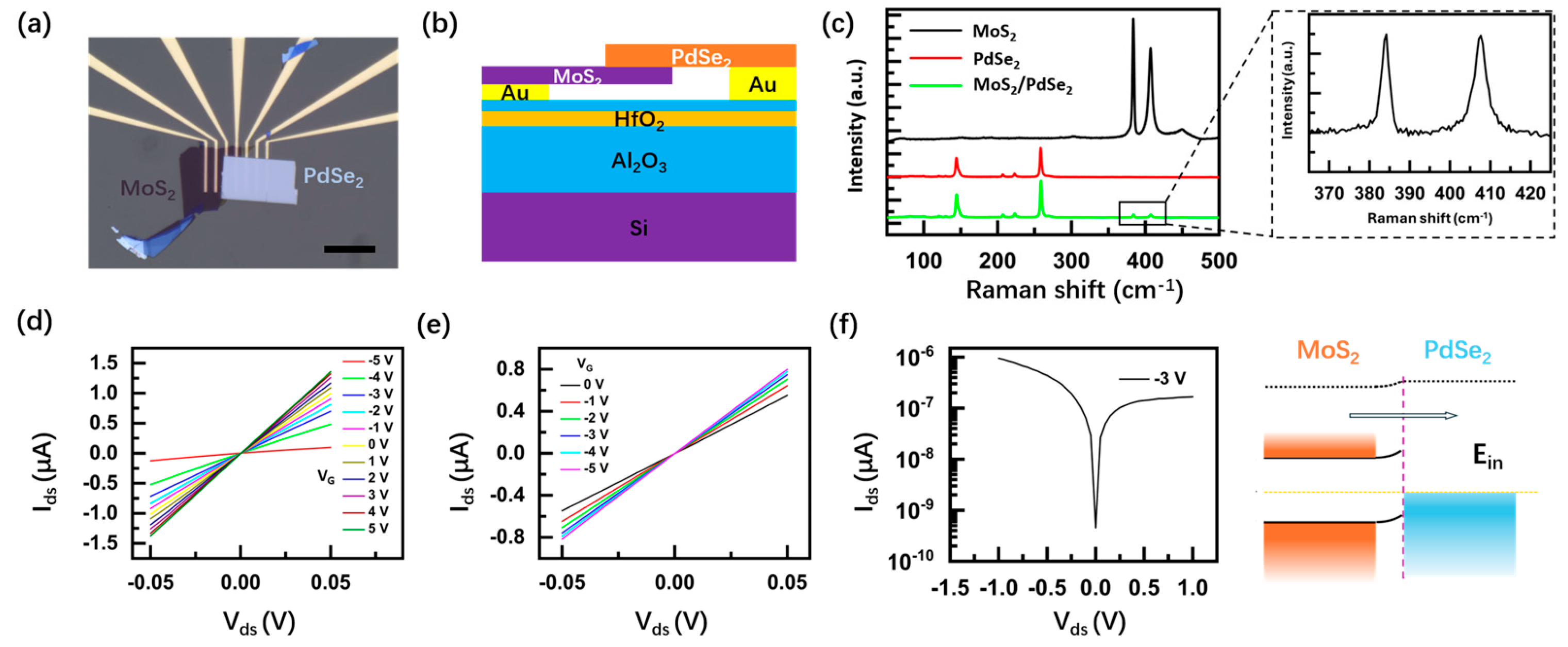
2 are subsequently exfoliated and stacked together (
Figure 1a). The schematic of MoS
2/PdSe
2 photodetector is shown in
Figure 1b.
Figure 1c shows the distinct Raman peaks of MoS
2/PdSe
2 heterostructure, which correspond to 382 cm
−1 (
) and 407 cm
−1 (
) for MoS
2 and 144 cm
−1 (
), 203 cm
−1 (
), 222 cm
−1 (
) and 258 cm
−1 (
) for PdSe
2.
Figure 1d and e show the I
ds–V
ds curves under different gate voltages V
G for MoS
2 and PdSe
2 field-effect transistor (FET), respectively. Notably, both of I
ds–V
ds curves demonstrate obvious linearity and it can be proved to be Ohmic source-drain contact for both FETs, which is necessary for optoelectronic characteristics of MoS
2/PdSe
2 photodetector. Furthermore, the output curves of I
ds–V
ds for MoS
2 FET exhibit a n-type ambipolar conducting behavior at V
G scanning from −5 to 5 V. By contrast, the current slightly increases with decreasing negative V
G for PdSe
2 FET, which indicates the semi-metallic behavior. Given the bandgaps of multilayer MoS
2 and PdSe
2 are previous reported to be 1.2 and 0.03 eV [
21,
22], the band alignment of MoS
2/PdSe
2 heterojunction is illustrated in
Figure 1f. The Schottky barrier can be formed at the interface of MoS
2/PdSe
2 heterojunction and the I
ds–V
ds curve exhibits a rectification behavior, demonstrating a rectification ratio I
on/ I
off up to 10.
3. Results
3.1. Transfer Characteristics and Static Memory Behavir
Charge-trap stack of Al
2O
3/HfO
2/ Al
2O
3 (6 nm/8 nm/32 nm) is deposited via atomic layer deposition (ALD).
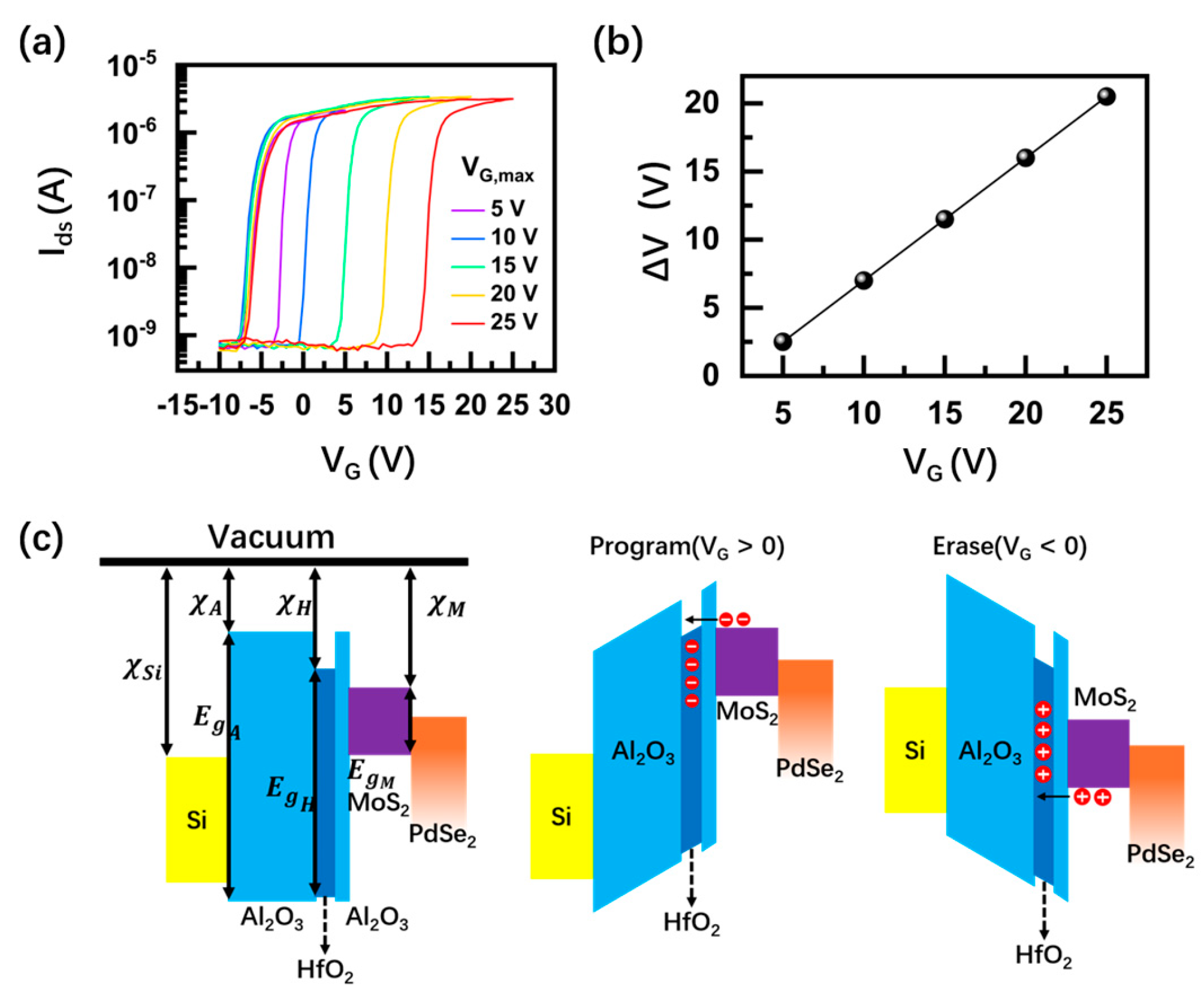
Figure 2a shows the transfer curves of MoS
2/PdSe
2 Schottky diode acquired by sweeping the gate voltage V
G in a closed loop (from negative to positive values) under a fixed V
ds of -1 V, exhibiting a clear hysteresis window and the hysteresis enables to widening as V
G sweep range increases from 5 to 25 V. The I
ds–V
G curves exhibit a clockwise memory window and the extraction of memory window ∆V increases almost linearly with the maximum V
G and reaches a maximum of 20 V when the V
G sweeps to 25 V (
Figure 2b). The transfer curve of I
ds–V
G decreases with increasing negative V
G, suggesting that n-type MoS
2 dominates the transfer characteristics of device.
Figure 2c illuminates the device operation process. When a high positive/negative V
G is applied to the gate, the band alignment starts favoring the tunnelling in/out of electrons from MoS
2/PdSe
2 channel to the HfO
2 charge-trap layer, changing the carrier concentration in MoS
2 and resulting into the program and erase state, respectively.
3.2. Dynamic Memory Behavir of Device
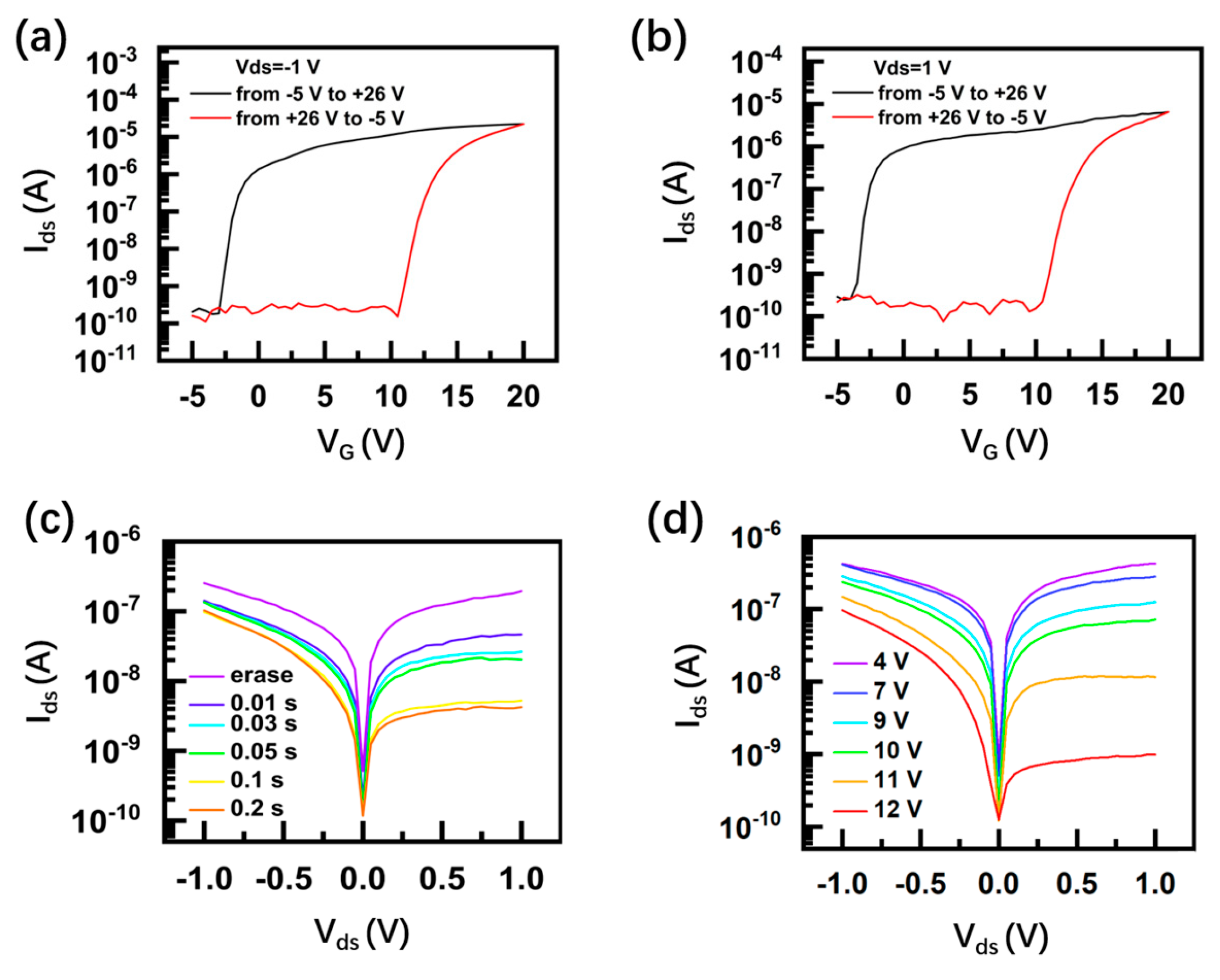
The transfer characteristics of device are further studied under different bias. As shown in
Figure 3a and 3b, they show that an obvious memory window under both forward bias of -1 V and reverse bias of +1 V, especially demonstrating a maximum program/erase current ratio of 10
5. To explore the dynamic transition of device, the device is initially set into erase state by applying a negative gate pulse (-10 V, duration of 2 s) and its output curves I
ds–V
ds are read by sweeping V
ds from -1 V to +1 V after applying a series of +25 V gate pulses with different duration times. The output curve I
ds–V
ds shows clear decrease and nearly saturated when the width of pulse increases to 0.2 s (
Figure 3c). According to the expression of charge-trapping rate [
23], the calculated charge-trapping rate varies from 10
15 to 10
14 cm
-2t
-1 when the pulse width changes from 0.01 s to 0.2 s.
Figure 3d shows the dependency of output curve I
ds–V
ds with amplitude of gate pulse. It demonstrates that output current decreases with the increase of pulse amplitude. It can be explained by modulation of Schottky barrier through the gate pulse, and it also suggests a charge-trapping mechanism of AHA gate stack dominates the memory behavior of device.
3.3. Photovoltaic Behavior and Reconfigurable Linear Polarization
Given the excellent memory switching properties of device (including unprecedented memory window, large program/erase current ratio and nonvolatile switchable Schottky barriers) and strong optical anisotropy of PdSe
2, the polarization-modulated photovoltaic behavior in the MoS
2/PdSe
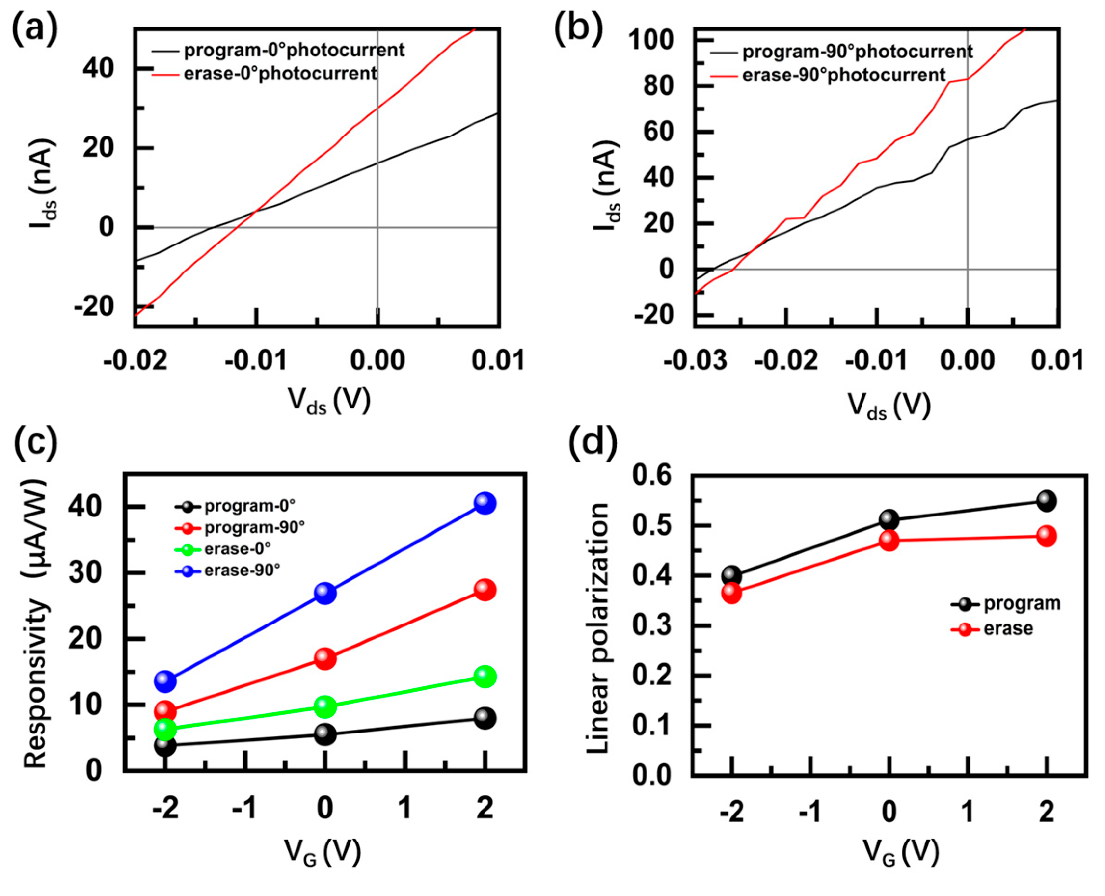
2-based photodetector is worthy of investigation. To characterize it, a positive (+25 V) and negative (-10 V) gate pulse with width of 0.2 s are applied to switch the device into program and erase state respectively. In program/erase state, I
ds–V
ds characteristics under illumination are recorded by using the polarized 520 nm light with intensity of 120 mW/cm
2.
Figure 4a and 4b show the I
ds–V
ds characteristics of device under parallel (
) and vertical (
) polarized light in the program and erase state, respectively (
and
directions correspond to the b-axis and a-axis crystalline direction of PdSe
2). It can be noticed that the device exhibits noticeable photovoltaic responses including a short-circuit current (I
sc) of ~15 nA/30 nA and an open-circuit voltage (V
oc) of ~-0.014 V/-0.012 V in program/erase state under parallel light excitation. After switching the polarization of light to vertical direction, the illuminated I
ds–V
ds curve shift toward the higher value, showing that I
sc and V
oc increase to ~54 nA/82 nA and ~-0.027/-0.025 V in program/erase state. In addition, gate voltage is applied to modulate the performance of device. The responsivity is extracted and plotted in
Figure 4c at different memory states and polarizations of light. The device shows a typical transfer characteristics of n-type MoS
2 semiconductor. As the gate voltage increases from -2 V to 2 V, all of responsivities increase at V
ds = -1 V. A figure of merit of the linear polarized photodetection is the degree of linear polarization (LP), where LP = (I
max - I
min)/(I
max + I
min), where I
max and I
min are the photocurrents of the detected light parallel and perpendicular to the primary polarization direction, respectively.
Figure 4d shows that the LP results as a function of V
G. Under 120 mW/cm
2 light illumination, both of LP of device gradually increases from 0.4/0.36 to 0.55/0.49 in the program/erase state. This indicates that the LP of device can be effectively modulated by the memory state and its gap between program and erase state become more obvious under the positive gate voltage.
4. Discussion
To understand the photoresponse mechanism of the MoS
2/PdSe
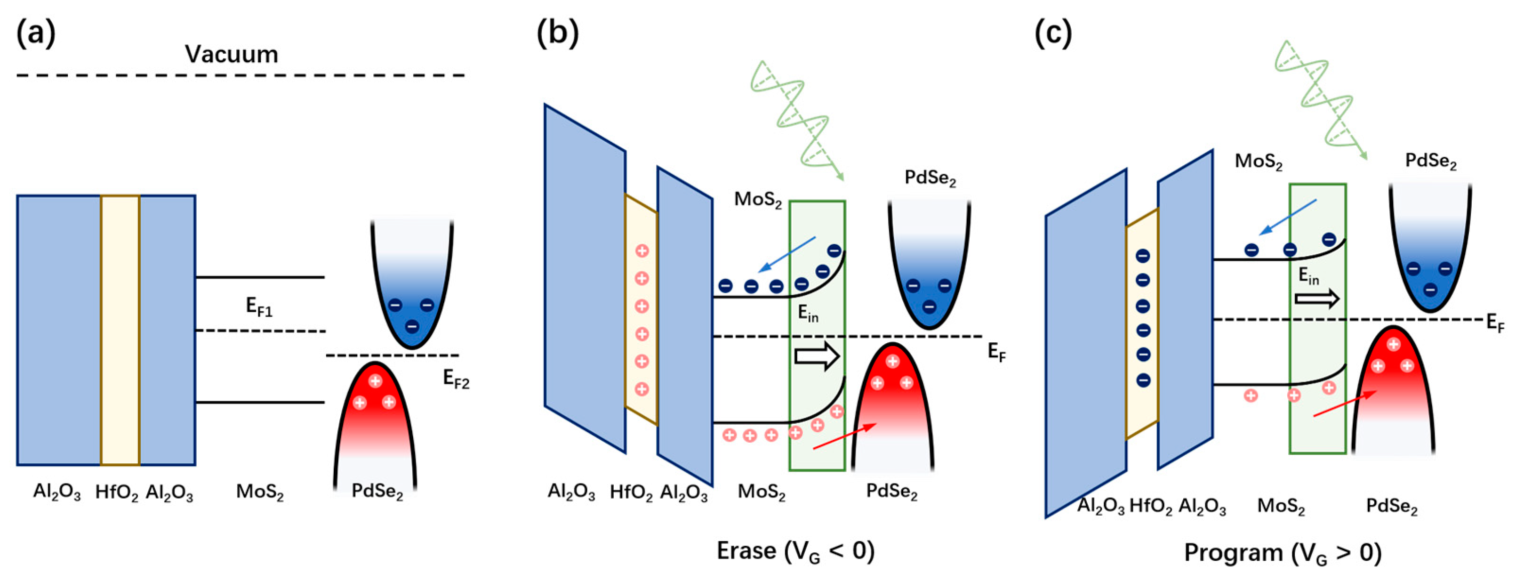
2 device, the energy band structure diagram was illustrated in
Figure 5. Since the fermi level of PdSe
2 is lower than MoS
2, the electrons will flow from MoS
2 to the PdSe
2, while the holes diffuse in opposite directions to MoS
2, introducing a Schottky barrier with the build-in field
Ein pointing from MoS
2 to PdSe
2 which is described in
Figure 1f. When the laser shines on the surface of the device, the electrons confined in the valence band will be excited to the conduction bands in both the two materials. Then with the help of build-in field Ein, the electrons occupied in PdSe
2 can be driven to the conduction band of MoS
2, while
Ein will force the holes within the MoS2 valence band to flow into the valence band of PdSe
2, resulting into the photovoltaic behavior. When the negative gate voltage pulse is applied to switch the device into erase state (
Figure 5b), the energy band of MoS
2 is lowered and Ein will increase, therefore enhancing the separation of photo-generated electron-hole pairs and short-circuit current. Meanwhile, the photocurrent generated from MoS
2 increase in the erase state, which results into the decrease of LP because of intrinsic polarization-insensitivity of MoS
2. On the other hand, the
Ein will be reduced in the program state (
Figure 5c), which induce to the decrease of short-circuit current and increase of LP. In this way, we can adjust the energy band structure of MoS
2/PdSe
2 by switching the program/erase state, thereby adjusting the photodetection performance of the device.
5. Conclusions
In summary, a multifunctional photovoltaic photodetector is demonstrated which is composed of in-plane anisotropic PdSe2 and MoS2 with AHA charge-trap gate stack. The device exhibits a nonvolatile phenomenon in both electrical and photovoltaic characteristics, resulting from the modulation of band alignment by the gate voltage pulse. Utilizing the AHA charge-trap gate stack, the memory window and program/erase current ratio of MoS2/PdSe2 can be effectively modulated. Acting as a reconfigurable polarimetric photodetector, the device exhibits a reversible performance of both responsivity and polarization-sensitive photocurrent by switching the program and erase state, rendering it a promising candidate for polarization signal recognition and imaging.
Author Contributions
C.Z. Gu and X. Huang conceived the research, Q.H. Bai and T. Liu fabricated the samples. Q.H. Bai conducted the measurements. All authors discussed the date and contributed to the manuscript.
Funding
This work was supported by the National Natural Science Foundation of China under Grant Nos. 62204259, 61888102, 92265110, 62174179, 11974386, 61905274, 12074420 and U21A20140, the National Key Research and Development Program of China under Grant No. 2021YFA1400700, the Key Research Program of Frontier Sciences of CAS under Grant Nos. QYZDJ-SSWSLH042 and XDPB22, the Project for Young Scientists in Basic Research of CAS under Grant No.YSBR021, the Guangdong Basic and Applied Basic Research Foundation under Grant No. 2023A1515010693. This work is also supported by the Synergic Extreme Condition User Facility, China.
Data Availability Statement
The data presented in this study are available on request from the corresponding author.
Conflicts of Interest
The authors declare no conflicts of interest.
References
- Hou, H.Y.; Tian, S.; Ge, H.R.; Chen, J.D.; Li, Y.Q.; Tang, J.X. Recent progress of polarization-sensitive perovskite photodetectors. Adv. Funct. Mater. 2022, 32, 2209324. [Google Scholar] [CrossRef]
- Wu, D.; Guo, J.; Du, J.; Xia, C.; Zeng, L.; Tian, Y.; Shi, Z.; Tian, Y.; Li, X.J.; Tsang, Y.H. Highly polarization-sensitive, broadband, self-powered photodetector based on graphene/PdSe2/germanium heterojunction. ACS Nano 2019, 13, 9907–9917. [Google Scholar] [CrossRef] [PubMed]
- Wang, J.; Jiang, C.; Li, W.; Xiao, X. Anisotropic low-dimensional materials for polarization-sensitive photodetectors: From materials to devices. Adv. Opt. Mater. 2022, 10, 2102436. [Google Scholar] [CrossRef]
- Guo, Z.; Cao, R.; Wang, H.; Zhang, X.; Meng, F.; Chen, X.; Gao, S.; Sang, D.K.; Nguyen, T.H.; Duong, A.T. High-performance polarization-sensitive photodetectors on two-dimensional β-InSe. Natl. Sci. Rev. 2022, 9, nwab098. [Google Scholar] [CrossRef]
- Huo, N.; Konstantatos, G. Recent progress and future prospects of 2D-based photodetectors. Adv. Mater. 2018, 30, 1801164. [Google Scholar] [CrossRef]
- Zhou, C.; Zhang, S.; Lv, Z.; Ma, Z.; Yu, C.; Feng, Z.; Chan, M. Self-driven WSe2 photodetectors enabled with asymmetrical van der Waals contact interfaces. npj 2D Mater. Appl. 2020, 4, 46. [Google Scholar] [CrossRef]
- Qiu, Q.; Huang, Z. Photodetectors of 2D materials from ultraviolet to terahertz waves. Adv. Mater. 2021, 33, 2008126. [Google Scholar] [CrossRef]
- Zhou, Z.; Long, M.; Pan, L.; Wang, X.; Zhong, M.; Blei, M.; Wang, J.; Fang, J.; Tongay, S.; Hu, W. Perpendicular optical reversal of the linear dichroism and polarized photodetection in 2D GeAs. ACS Nano 2018, 12, 12416–12423. [Google Scholar] [CrossRef]
- Yuan, H.; Liu, X.; Afshinmanesh, F.; Li, W.; Xu, G.; Sun, J.; Lian, B.; Curto, A.G.; Ye, G.; Hikita, Y. Polarization-sensitive broadband photodetector using a black phosphorus vertical p–n junction. Nat. Nanotechnol. 2015, 10, 707–713. [Google Scholar] [CrossRef]
- Liu, F.; Zheng, S.; He, X.; Chaturvedi, A.; He, J.; Chow, W.L.; Mion, T.R.; Wang, X.; Zhou, J.; Fu, Q. Highly sensitive detection of polarized light using anisotropic 2D ReS2. Adv. Funct. Mater. 2016, 26, 1169–1177. [Google Scholar] [CrossRef]
- Li, L.; Gong, P.; Sheng, D.; Wang, S.; Wang, W.; Zhu, X.; Shi, X.; Wang, F.; Han, W.; Yang, S. Highly in-plane anisotropic 2D GeAs2 for polarization-sensitive photodetection. Adv. Mater. 2018, 30, 1804541. [Google Scholar] [CrossRef] [PubMed]
- Wang, X.; Shang, J.; Zhu, M.; Zhou, X.; Hao, R.; Sun, L.; Xu, H.; Zheng, J.; Lei, X.; Li, C. Controlled growth of large-scale uniform 1T′-MoTe2 crystals with tunable thickness and their photodetector applications. Nanoscale Horiz. 2020, 5, 954–959. [Google Scholar] [CrossRef] [PubMed]
- Xu, Z.; Luo, B.; Chen, Y.; Li, X.; Chen, Z.; Yuan, Q.; Xiao, X. High sensitivity and anisotropic broadband photoresponse of Td-WTe2. Phys. Lett. A 2021, 389, 127093. [Google Scholar] [CrossRef]
- Ahn, J.; Ko, K.; Kyhm, J.-h.; Ra, H.-S.; Bae, H.; Hong, S.; Kim, D.-Y.; Jang, J.; Kim, T.W.; Choi, S. Near-infrared self-powered linearly polarized photodetection and digital incoherent holography using WSe2/ReSe2 van der Waals heterostructure. ACS Nano 2021, 15, 17917–17925. [Google Scholar] [CrossRef]
- Xiong, J.; Dan, Z.; Li, H.; Li, S.; Sun, Y.; Gao, W.; Huo, N.; Li, J. Multifunctional GeAs/WS2 heterojunctions for highly polarization-sensitive photodetectors in the short-wave infrared range. Acs. Appl. Mater. Inter. 2022, 14, 22607–22614. [Google Scholar] [CrossRef]
- Jiang, J.; Xu, W.; Guo, F.; Yang, S.; Ge, W.; Shen, B.; Tang, N. Polarization-resolved near-infrared PdSe2 pin homojunction photodetector. Nano Lett. 2023, 23, 9522–9528. [Google Scholar] [CrossRef]
- Huang, M.; Luo, S.; Qiao, H.; Yao, B.; Huang, Z.; Wang, Z.; Bao, Q.; Qi, X. Ferroelectric polarization enhanced photodetector based on layered NbOCl2. Small Science 2024, 4, 2300246. [Google Scholar] [CrossRef]
- Wu, G.; Zhang, X.; Feng, G.; Wang, J.; Zhou, K.; Zeng, J.; Dong, D.; Zhu, F.; Yang, C.; Zhao, X. Ferroelectric-defined reconfigurable homojunctions for in-memory sensing and computing. Nat. Mater. 2023, 22, 1499–1506. [Google Scholar] [CrossRef]
- Zhou, G.; Li, J.; Song, Q.; Wang, L.; Ren, Z.; Sun, B.; Hu, X.; Wang, W.; Xu, G.; Chen, X. Full hardware implementation of neuromorphic visual system based on multimodal optoelectronic resistive memory arrays for versatile image processing. Nat. Commun. 2023, 14, 8489. [Google Scholar] [CrossRef]
- Zhang, G.-X.; Zhang, Z.-C.; Chen, X.-D.; Kang, L.; Li, Y.; Wang, F.-D.; Shi, L.; Shi, K.; Liu, Z.-B.; Tian, J.-G. Broadband sensory networks with locally stored responsivities for neuromorphic machine vision. Sci. Adv. 2023, 9, eadi5104. [Google Scholar] [CrossRef]
- Long, M.; Wang, Y.; Wang, P.; Zhou, X.; Xia, H.; Luo, C.; Huang, S.; Zhang, G.; Yan, H.; Fan, Z. Palladium diselenide long-wavelength infrared photodetector with high sensitivity and stability. ACS Nano 2019, 13, 2511–2519. [Google Scholar] [CrossRef] [PubMed]
- Kang, J.; Tongay, S.; Zhou, J.; Li, J.; Wu, J. Band offsets and heterostructures of two-dimensional semiconductors. Appl. Phys. Lett. 2013, 102. [Google Scholar] [CrossRef]
- Sup Choi, M.; Lee, G.-H.; Yu, Y.-J.; Lee, D.-Y.; Hwan Lee, S.; Kim, P.; Hone, J.; Jong Yoo, W. Controlled charge trapping by molybdenum disulphide and graphene in ultrathin heterostructured memory devices. Nat. Commun. 2013, 4, 1624. [Google Scholar] [CrossRef] [PubMed]
|
Disclaimer/Publisher’s Note: The statements, opinions and data contained in all publications are solely those of the individual author(s) and contributor(s) and not of MDPI and/or the editor(s). MDPI and/or the editor(s) disclaim responsibility for any injury to people or property resulting from any ideas, methods, instructions or products referred to in the content. |
© 2024 by the authors. Licensee MDPI, Basel, Switzerland. This article is an open access article distributed under the terms and conditions of the Creative Commons Attribution (CC BY) license (http://creativecommons.org/licenses/by/4.0/).
