Submitted:
04 November 2024
Posted:
05 November 2024
You are already at the latest version
Abstract
Keywords:
1. Introduction
2. System Design
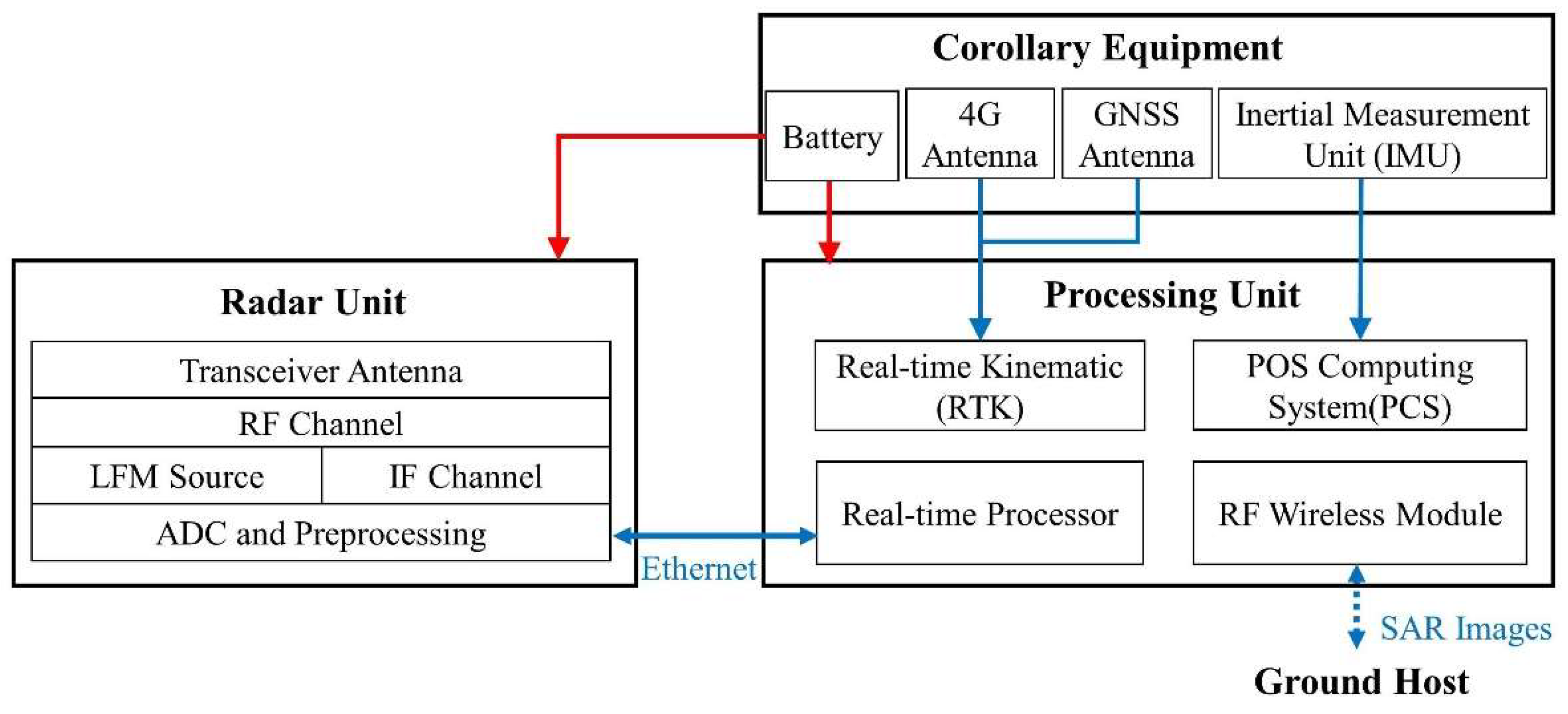
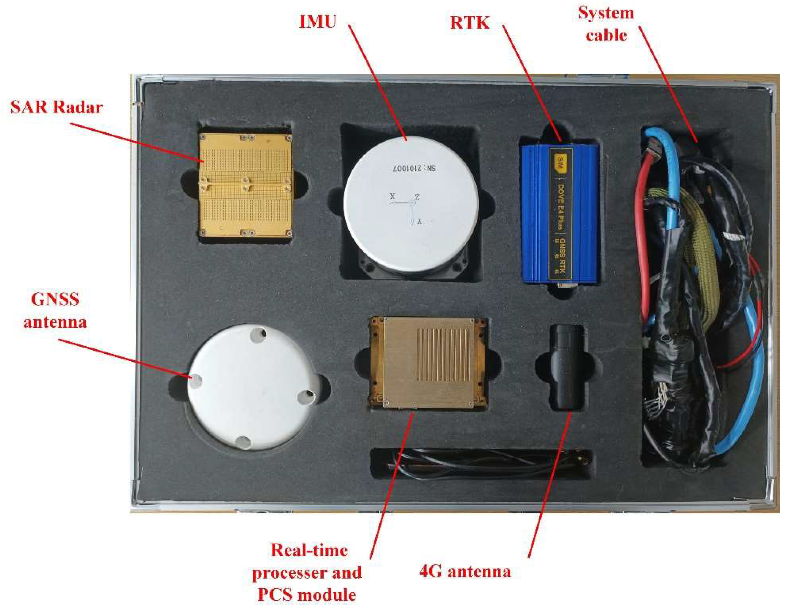
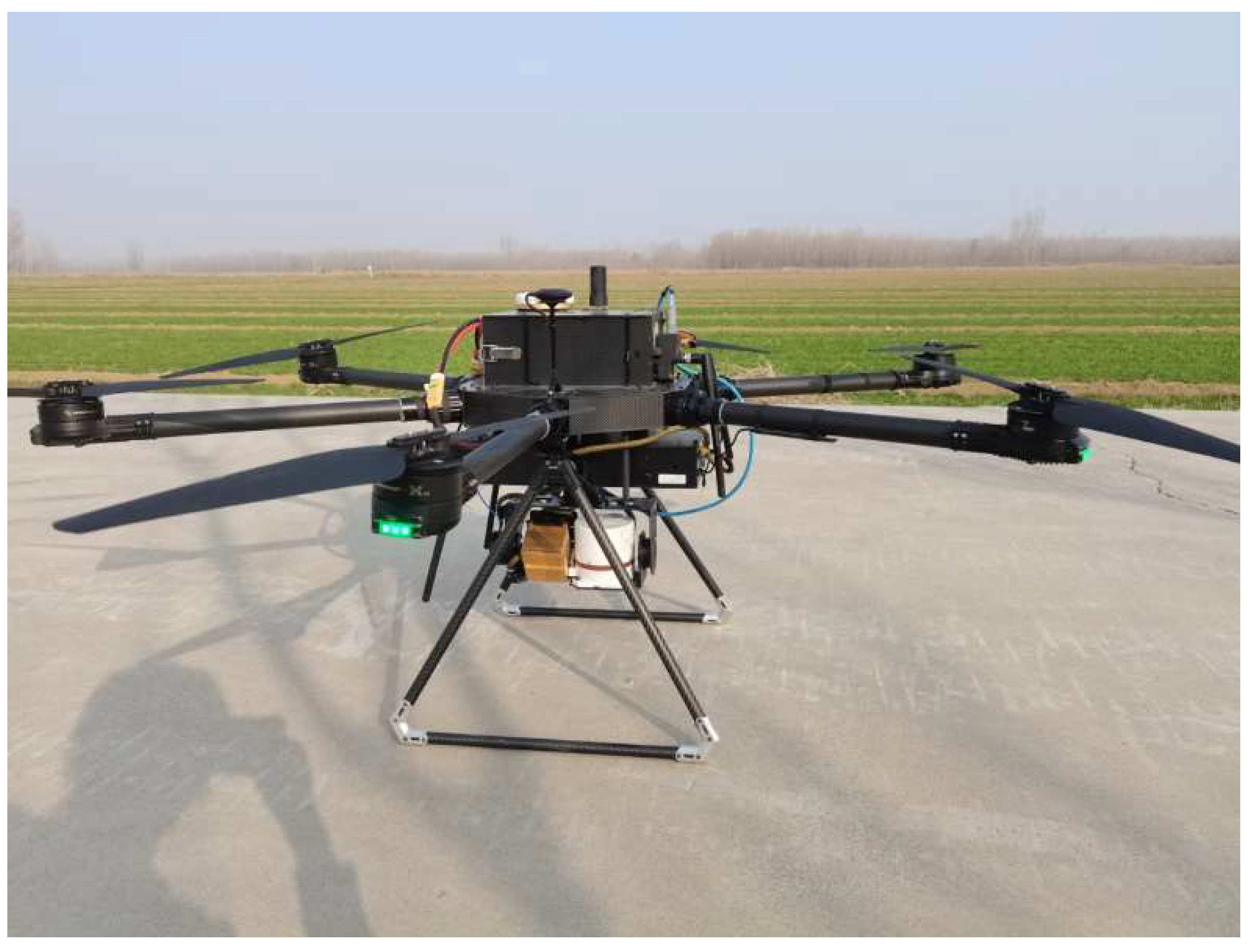
2.1. System Architecture for Real-Time Imaging Mini-SAR System
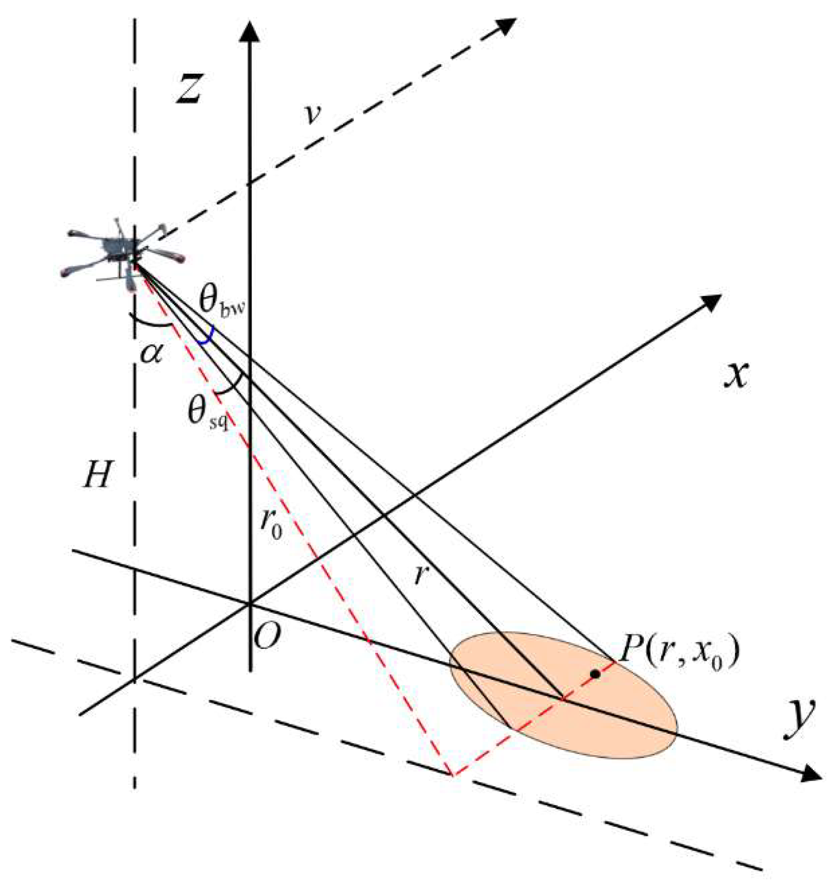
2.2. System Performance Indicators
3. Key Technologies
3.1. Data Preprocessing Algorithm
3.2. Real-Time Processing Algorithms and Hardware Acceleration
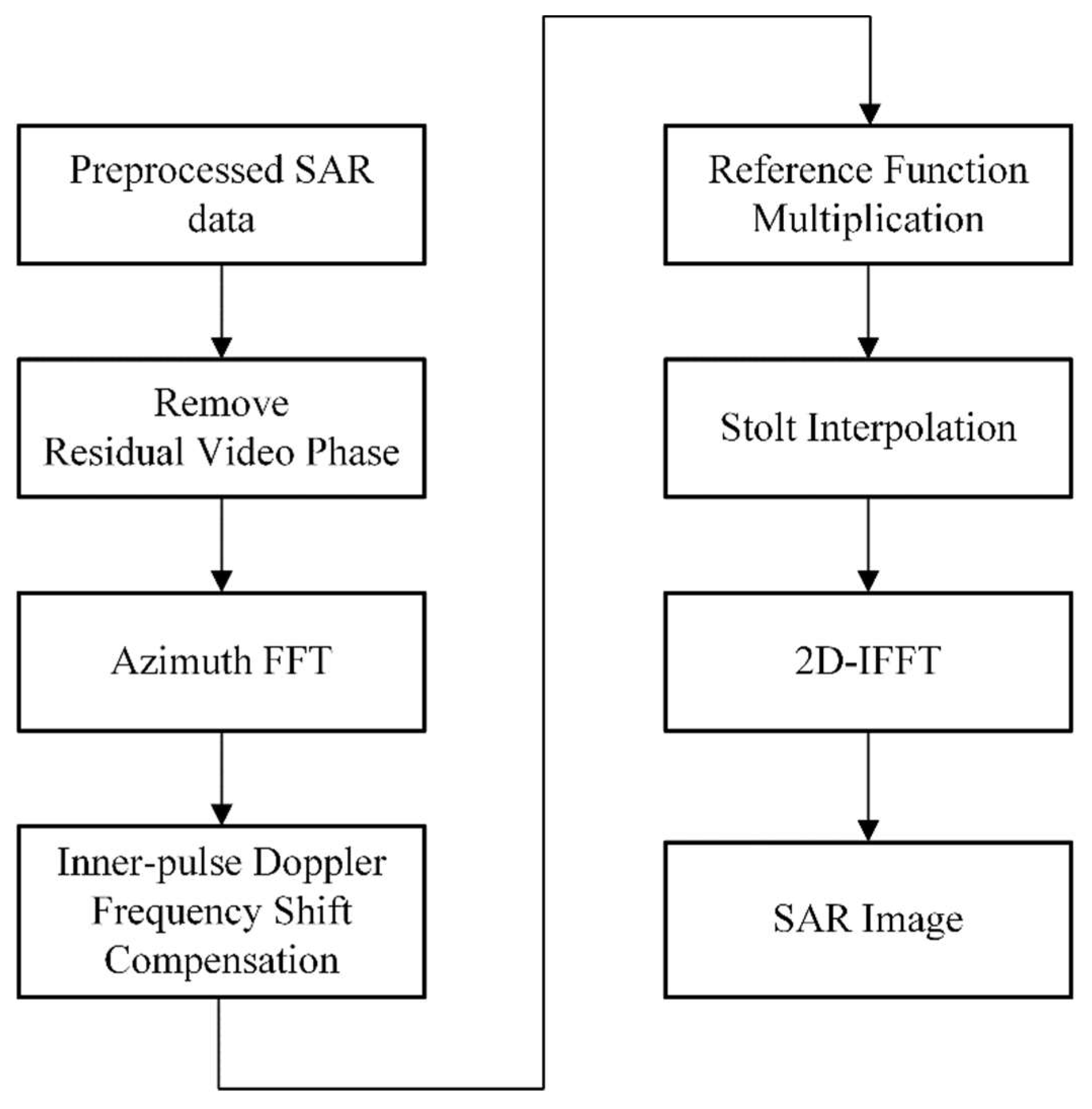
3.2.1. Principles and Structural Analysis of the ω-k Algorithm
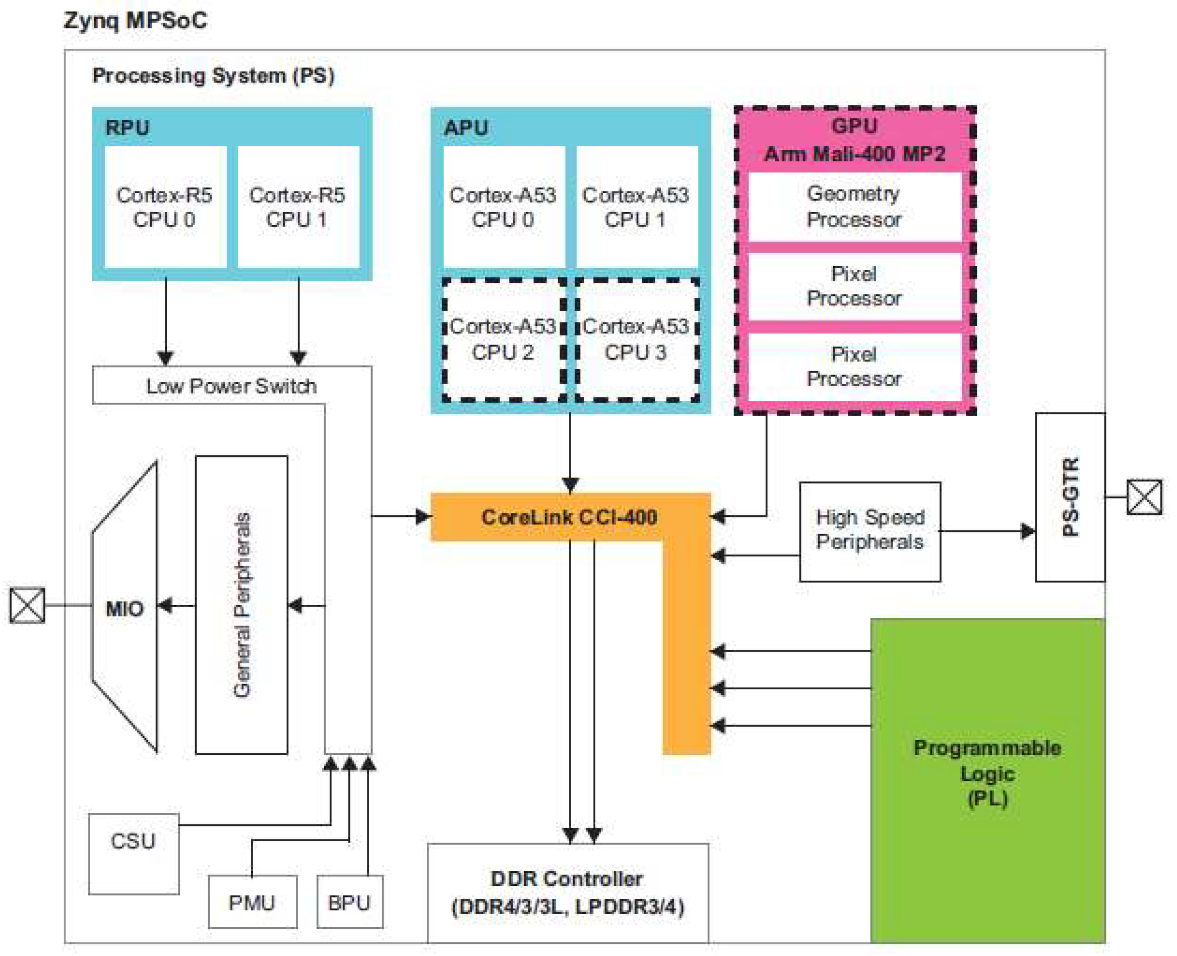
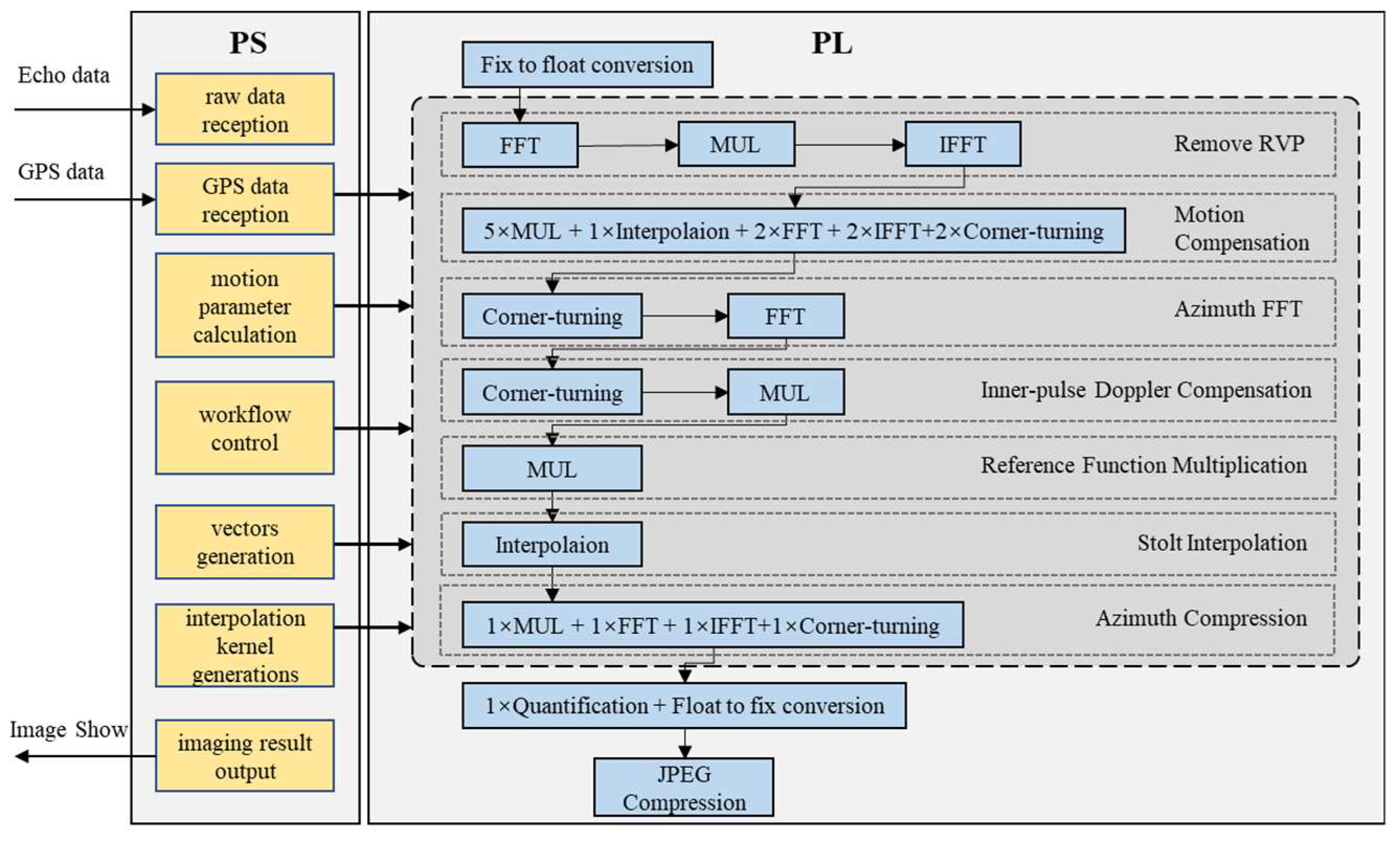
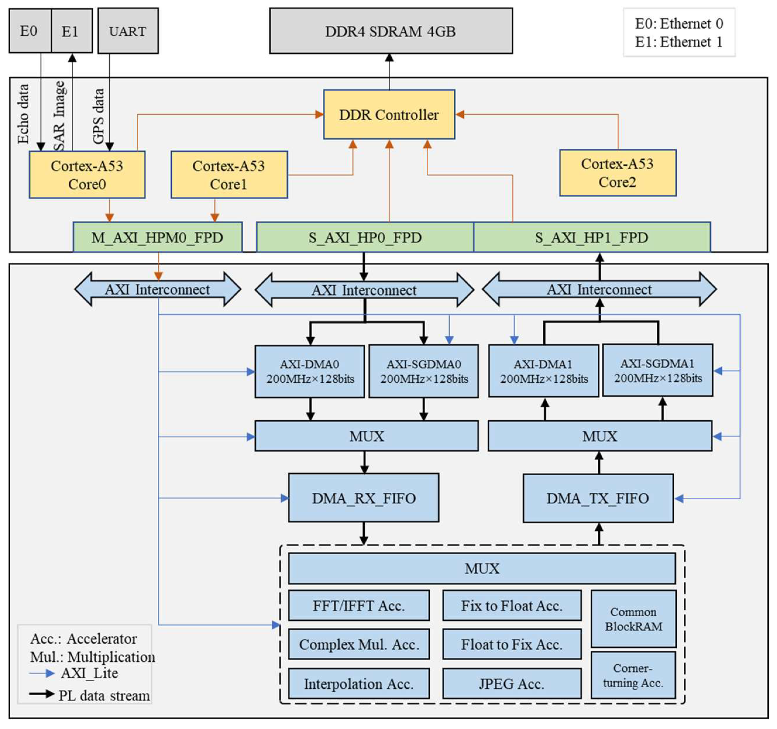
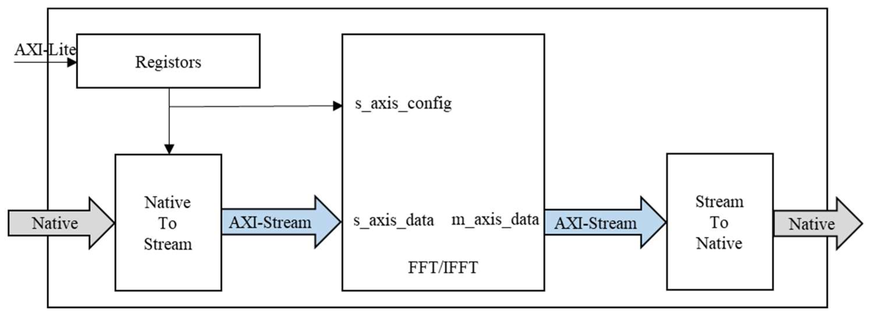
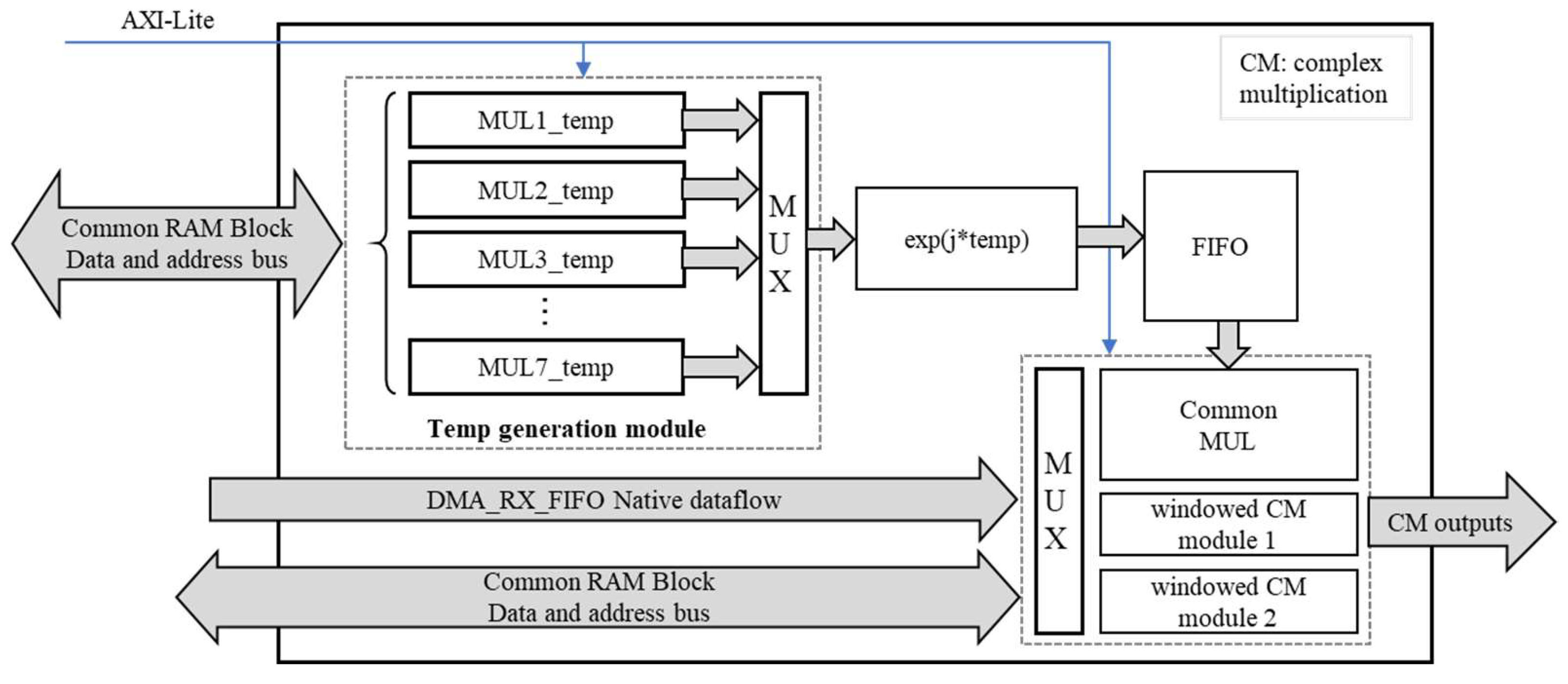
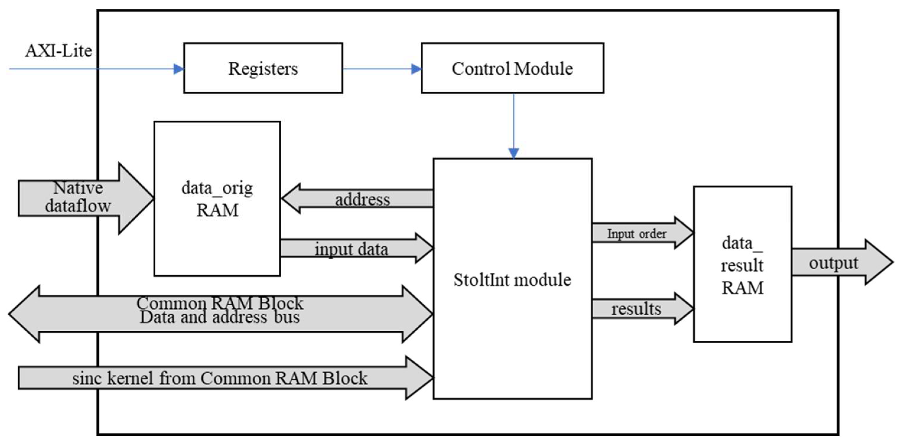
3.2.2. SAR Real-Time Processing on MPSoC
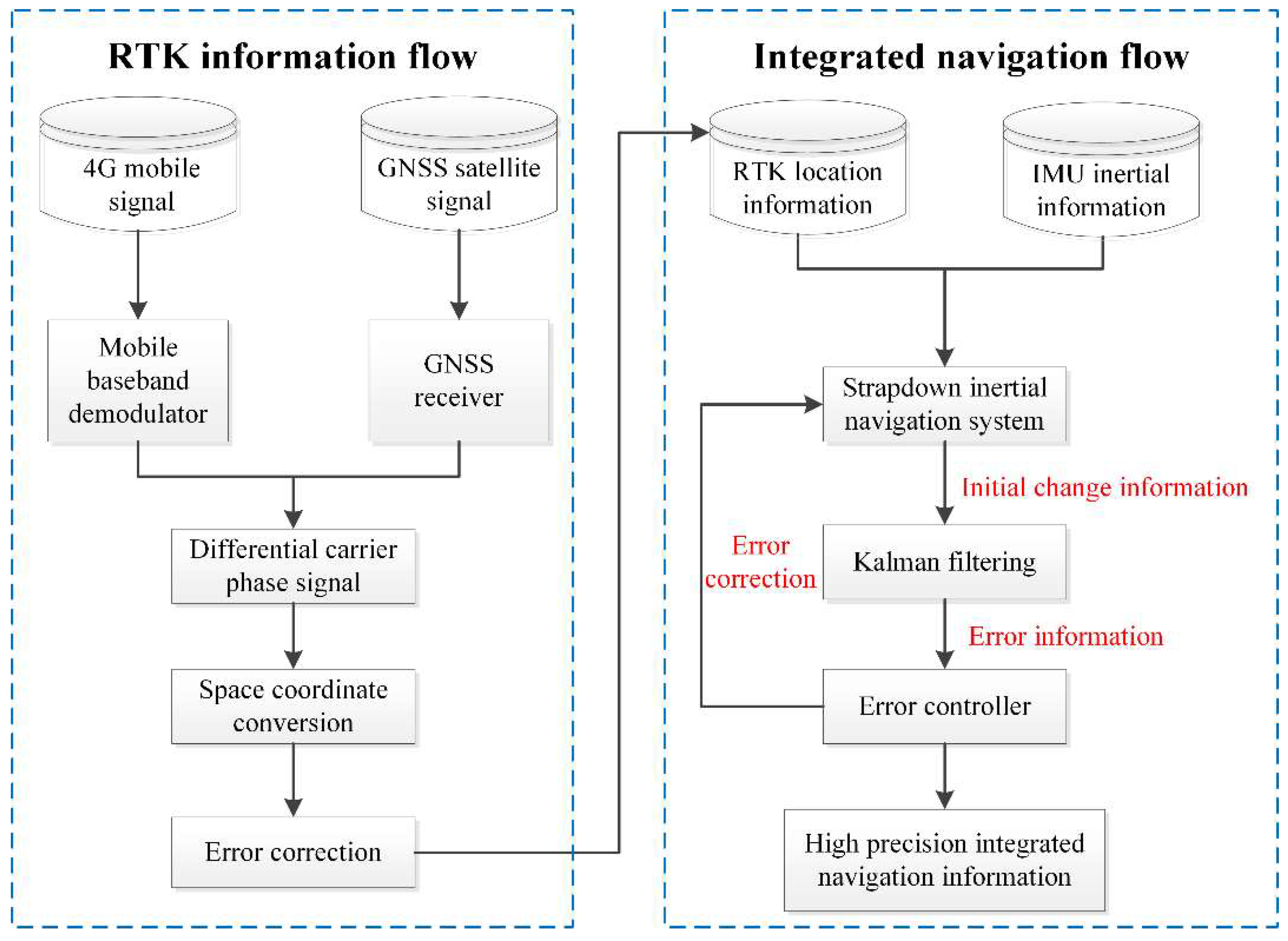
3.3. Lightweight and High-Precision Real-Time Motion Compensation System
4. Results
115. Conclusions
Author Contributions
Funding
Data Availability Statement
Acknowledgments
Conflicts of Interest
References
- Xie, W. Research on Target Extraction System of UAV Remote Sensing Image Based on Artificial Intelligence. In Proceedings of the IEEE International Conference on Integrated Circuits Communication Systems, 2023; pp. 1-5.
- Yang, Z.; Yu, X.; Dedman, S.; Rosso, M.; Zhu, J.; Yang, J.; Xia, Y.; Tian, Y.; Zhang, G.; Wang, J. UAV remote sensing applications in marine monitoring: Knowledge visualization and review. The Science of the total environment 2022, 155939. [CrossRef]
- Lyu, X.; Li, X.; Dang, D.; Dou, H.; Wang, K.; Lou, A.J.R.S. Unmanned Aerial Vehicle (UAV) Remote Sensing in Grassland Ecosystem Monitoring: A Systematic Review. 2022, 14, 1096. [CrossRef]
- Sothe, C.; Dalponte, M.; Almeida, C.M.d.; Schimalski, M.B.; Lima, C.L.; Liesenberg, V.; Miyoshi, G.T.; Tommaselli, A.M.G.J.R.S. Tree Species Classification in a Highly Diverse Subtropical Forest Integrating UAV-Based Photogrammetric Point Cloud and Hyperspectral Data. 2019, 11, 1338. [CrossRef]
- Du, M.; Noguchi, N.J.R.S. Monitoring of Wheat Growth Status and Mapping of Wheat Yield’s within-Field Spatial Variations Using Color Images Acquired from UAV-camera System. 2017, 9, 289. [CrossRef]
- Caris, M.; Stanko, S.; Palm, S.; Sommer, R.; Pohl, N. Synthetic aperture radar at millimeter wavelength for UAV surveillance applications. In Proceedings of the IEEE 1st International Forum on Research Technologies for Society Industry Leveraging a better tomorrow, Turin, Italy, 16-18 September 2015.
- Dill, S.; Schreiber, E.; Engel, M.; Heinzel, A.; Peichl, M. A drone carried multichannel Synthetic Aperture Radar for advanced buried object detection. In Proceedings of the IEEE Radar Conference, Boston, USA, 22-26 April 2019. [CrossRef]
- Ding, M.; Wang, X.; Tang, L.; Qu, J.-M.; Wang, Y.; Zhou, L.; Wang, B.J.R.S. A W-Band Active Phased Array Miniaturized Scan-SAR with High Resolution on Multi-Rotor UAVs. 2022, 14, 5840. [CrossRef]
- Li, W.; Chen, X.; Li, G.; Bi, Y. Construction of Yunnan’s Agricultural Ecological Civilization Based on Intelligent UAV and SAR Image Analysis. In Proceedings of the 4th International Conference on Smart Systems Inventive Technology, Tirunelveli, India, 20-22 January 2022.
- Lort, M.; Aguasca, A.; López-Martínez, C.; Marín, T.M.J.I.J.o.S.T.i.A.E.O.; Sensing, R. Initial Evaluation of SAR Capabilities in UAV Multicopter Platforms. 2018, 11, 127-140. [CrossRef]
- Ding, M.; Ding, C.; Tang, L.; Wang, X.; Qu, J.-M.; Wu, R. A W-Band 3-D Integrated Mini-SAR System With High Imaging Resolution on UAV Platform. IEEE Access 2020, 8, 113601-113609. [CrossRef]
- Cao, Y.; Jiang, S.; Guo, S.; Ling, W.; Zhou, X.; Yu, Z. Real-Time SAR Imaging Based on Reconfigurable Computing. IEEE Access 2021, 9, 93684-93690, doi:10.1109/ACCESS.2021.3093299. [CrossRef]
- Jia, G.; Buchroithner, M.; Chang, W.; Li, X. Simplified real-time imaging flow for high-resolution FMCW SAR. IEEE Geoscience Remote Sensing Letters 2014, 12, 973-977.
- Wu, W.; Zhang, Y.; Li, Z.; Yang, H.; Wu, J.; Yang, J. A Novel High Efficiency SAR Real-Time Processing System. In Proceedings of the IGARSS 2022-2022 IEEE International Geoscience and Remote Sensing Symposium, 2022; pp. 3401-3403.
- Yu, W.; Xie, Y.; Lu, D.; Li, B.; Chen, H.; Chen, L. Algorithm implementation of on-board SAR imaging on FPGA+ DSP platform. In Proceedings of the 2019 IEEE International Conference on Signal, Information and Data Processing (ICSIDP), 2019; pp. 1-5.
- Yang, T.; Xu, Q.; Meng, F.; Zhang, S. Distributed Real-Time Image Processing of Formation Flying SAR Based on Embedded GPUs. IEEE Journal of Selected Topics in Applied Earth Observations Remote Sensing 2022, 15, 6495-6505. [CrossRef]
- Tang, L.; Qu, J.; Wang, X.; Ding, M.; Wang, Y.; Wang, B. An Efficient Real-Time Data Compression Method for Frequency-Modulated Continuous Wave SAR. In Proceedings of the 2024 IEEE International Geoscience and Remote Sensing Symposium, Athens, Greece, 2024.
- Xilinx, I. Zynq UltraScale+ Device Technical Reference Manual, v1.9 ed.; 2019.
- Xuan, Z.; Zhongjun, Y.; Yue, C.; Shuai, J. A FPGA implementation of ω⁃k algorithm. Electronic Design Engineering 2020, 28, 6.
- Yang, C.; Li, B.; Chen, L.; Wei, C.; Xie, Y.; Chen, H.; Yu, W.J.S. A Spaceborne Synthetic Aperture Radar Partial Fixed-Point Imaging System Using a Field- Programmable Gate Array—Application-Specific Integrated Circuit Hybrid Heterogeneous Parallel Acceleration Technique. 2017, 17. [CrossRef]
- Fang, R.; Sun, G.; Liu, Y.; Xing, M.-d.; Zhang, Z.-j.J.r.C.I.S.S. SAR real-time imaging pipeline technology based on multi-core DSP. 2022, 1-4.
- Shan-qing, H.; Hui-xing, L.; Bing-yi, L.; Yi-zhuang, X.; Liang, C.; He, C.J.T.o.B.i.o.T. The real-time imaging method for sliding spotlight SAR based on embedded GPU. Transactions of Beijing institute of Technology 2020, 40, 1018-1025.
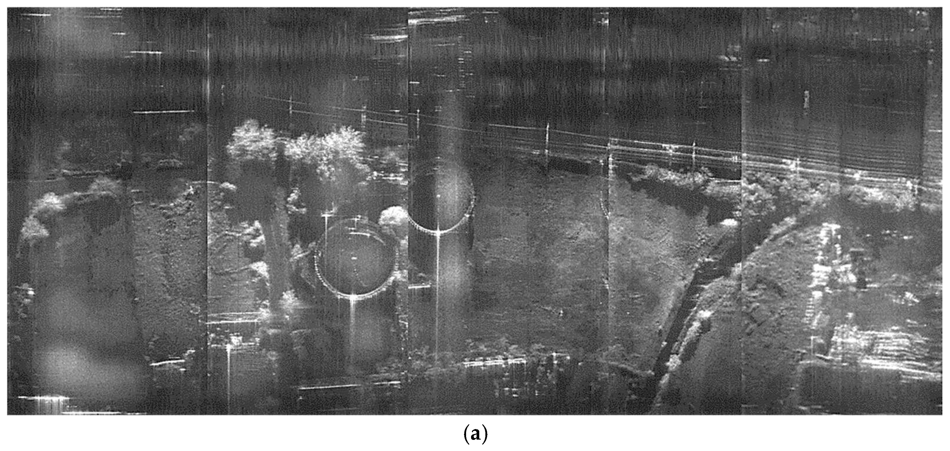

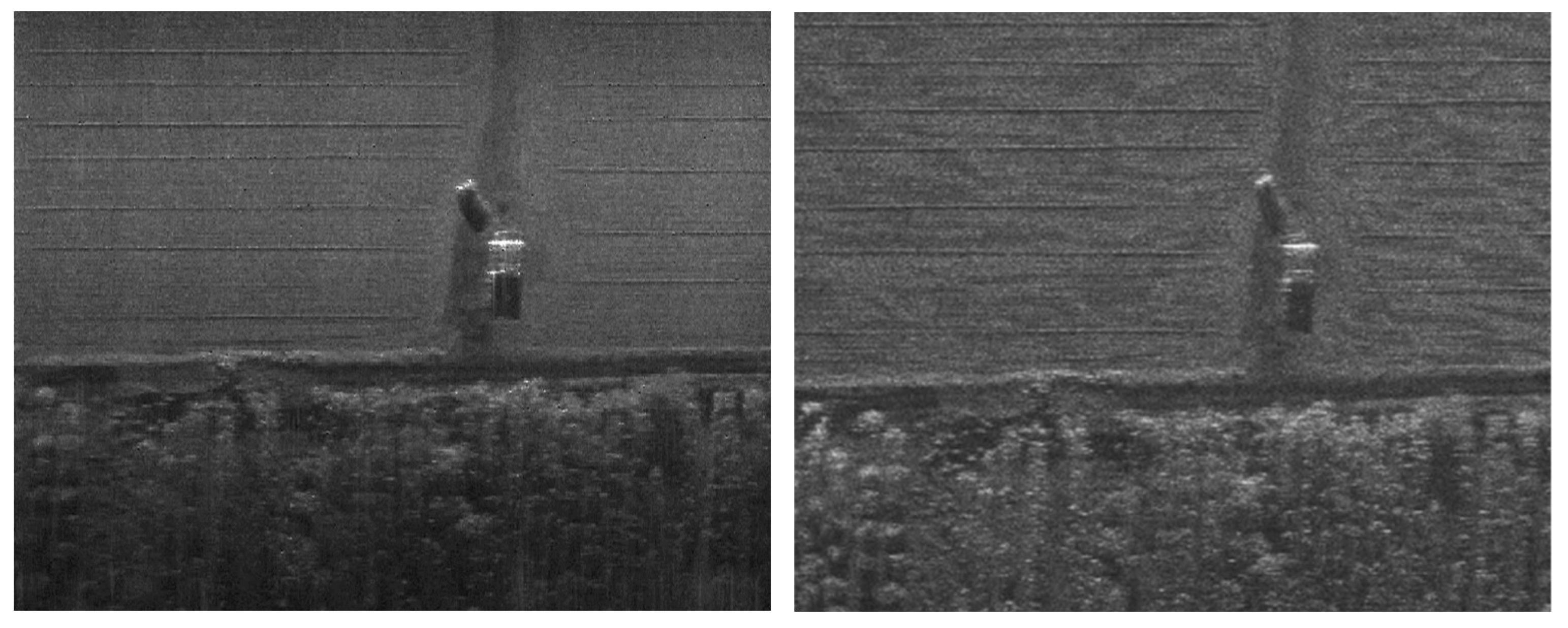
| Parameter | Value |
|---|---|
| Center frequency | 94 GHz |
| Maximum bandwidth | 4 GHz |
| Beamwidth Action distance |
12° × 3° |
| 600 m | |
| Resolution | ≤ 0.05 m |
| Real-time imaging size | 4k x 4k |
| Processing delay | 4.5 s |
| Real-time imaging error | ≤ 10⁻⁴ |
| Volume | 67 × 60 × 50 mm³ (Radar Unit) |
| Weight | 724 g |
| Power consumption | 38.3 watts |
| Module/Unit | Size | Weight/g | Power consumption/watts |
|---|---|---|---|
| SAR radar | 67×60×50 mm3 | 400 | 24 |
| Real-time processor | 60×60×18 mm3 | 110 | 10 |
| PCS | 67×60×14.6 mm3 | 120 | 2.5 |
| RTK | 92×54×26.5 mm3 | 94 | 1.8 |
| IMU | 90 mm (Φ)×90 mm (H) | 955 | 5.6 |
| GNSS antenna | 89 mm (Φ)×41.5 mm (H) | 195 | / |
| 4G antenna | 27.5 mm (Φ)×55.6 mm (H) | 18 | / |
| Cables | / | 280 | / |
| Module | LUT | Block RAM | DSP |
|---|---|---|---|
| FFT/IFFT | 8011 | 53 | 60 |
| Corner Turning | 197 | 120 | 0 |
| Complex Multiplication | 56572 | 1 | 477 |
| Interpolation | 68052 | 42 | 373 |
| Common Block RAM | 794 | 144 | 0 |
| Fix to Float Conversion | 744 | 4 | 0 |
| Quantification & Float to Fix conversion |
1361 | 1 | 8 |
| JPEG Compression | 4941 | 8.5 | 9 |
| AXI DMA | 3987 | 8.5 | 0 |
| FIFO | 258 | 2 | 0 |
| Other | 9024 | 0 | 0 |
| Total | 153941 | 384 | 927 |
| Available | 274080 | 912 | 2520 |
| Utilization | 56.2% | 42.1% | 36.8% |
| Steps | Modules | Time |
|---|---|---|
| Data Reception | LwIP | 865.92 ms |
| Real-Time Imaging | Fix to Float Conversion ×1 | 83.91 ms |
| FFT/IFFT ×9 | 755.37 ms | |
| Complex Multiplication ×9 | 755.19 ms | |
| Interpolation ×2 | 167.99 ms | |
| Corner Turning ×5 | 563.94 ms | |
| Quantification and Float-to-Fix Conversion ×1 | 83.91 ms | |
| JPEG ×1 | 83.92 ms | |
| PS Control、Small Batch Computing | 1005.32 ms | |
| Image Output | LwIP | 21.82 ms |
| Total | 2 times LwIP, 28 times acc. | 4387.29 ms |
| Ref. | Processor | Algorithm | Image Size | Time Consumption / s |
Power Consumption / watts |
Performance-to-Power Ratio / % | Verification |
|---|---|---|---|---|---|---|---|
| [12] | FPGA (XC7VX690T) |
CSA | 65536 × 65536 | 85.9 | 38.5 | 1.24 | Image |
| [20] | FPGA+ASIC | CSA | 16384 × 16384 | 12 | 21 | 1.02 | Image |
| [21] | 4-chip DSP (C6678) |
Real-Time Unified Focusing Algorithm (RT-UFA) |
8192 × 128 | 0.031 | 46 | 0.70 | Image |
| [14] | 2 FPGAs+ 6 DSPs |
RDA + PGA | 1024 × 1024 | 0.462 | 48 | 0.05 | Image |
| [22] | GPU (Jetson TX2) |
CSA | 16384 × 8192 | 12.66 | 15 | 0.67 | Image |
| [16] | GPU (Jetson Nano) |
CSA | 8192 × 8192 | 5.86 | 5 | 0.55 | Image |
| This work | Xilinx Zynq Ultrascale+ZU9EG MPSoC | ω-k | 4096 × 4096 | 4.5 | 10 | 0.35 | Flight Test |
Disclaimer/Publisher’s Note: The statements, opinions and data contained in all publications are solely those of the individual author(s) and contributor(s) and not of MDPI and/or the editor(s). MDPI and/or the editor(s) disclaim responsibility for any injury to people or property resulting from any ideas, methods, instructions or products referred to in the content. |
© 2024 by the authors. Licensee MDPI, Basel, Switzerland. This article is an open access article distributed under the terms and conditions of the Creative Commons Attribution (CC BY) license (http://creativecommons.org/licenses/by/4.0/).


