
Submitted:
17 November 2024
Posted:
19 November 2024
You are already at the latest version
Abstract
Nanomaterials used can significantly improve the analytical performance of optical sensors to environmental pollutants. Two-dimensional (2D) molybdenum sulfide (MoS2) exhibits some unique physicochemical properties such as strong light-matter interaction, bandgap tunability, and high carrier mobility, which are beneficial for constructing flexible optoelectronic devices. In this Review, the principle and classification of 2D MoS2-based photodetectors (PDs) are introduced, followed by a discussion about the physicochemical properties of 2D MoS2, as well as structure-property relationships of 2D MoS2-based photoactive materials for PDs to understand the modulation strategies for enhancing the photodetection performance. Furthermore, we discuss significant advances in the surface modification and functionalization of 2D MoS2 for developing high-performance PDs, particularly focusing on synthesis pathways, modification strategies, and underlying physiochemical mechanisms for enhanced photodetection capabilities. Finally, conclusions and research perspectives on resolving significant bottlenecks or remaining challenges are offered based on recent developments in 2D MoS2-based PDs.
Keywords:
2D nanomaterials
; photodetectors
; plasmon
; heterojunction
; functionalization
1. Introduction
Photodetectors (PDs) play an important role in various fields, such as environmental monitoring, imaging, and optical communication [1,2,3]. PDs can be used to analyze the concentration of harmful gases in the air and/or pollutants in water environment by measuring the degree of light absorption of them. This is quite important for environmental sustainability and national sustainable development strategy, because environmental pollution with its health impacts is a key issue for sustainable environment, which requires the precise analysis or prediction of environmental pollution and the decrease of waste production for preventing threat to human health and Earth’s ecosystems. Trace pollutants in water are detected mainly based on the Beer-Lambert law in the whole concentration range so that the absorption peaks of pollutants can be effectively measured with PDs. For example, highly sensitive and accurate monitoring of trace dye pollutants/chlorophyllin A analogue in water environment with a detection limit of 0.02/0.05 mg·L−1 (below the discharge/eutrophication standard) is successfully accomplished with PDs, surpassing the commercial Si photodiode that cannot effectively respond to the concentration below the standard [4]. The dual-functional device can act as not only a high-performance PD but also a highly sensitive gas sensor, such as O3, H2, CO, NO, and NO2 [5]. The gas sensor can be widely used to in situ detect various of gas pollutants in different application scenes [6,7,8,9,10,11].
The basic principle of PDs is to transform optical signals into electrical signals, in which using semiconductors as photoactive materials (as the critical components in PDs) with wide broad spectrum response, low dark current, excellent photoresponsivity, and low response time, can possess more advantages for constructing high-performance PDs [12]. This process involves the generation, separation, and transport of photogenerated charge carriers, as well as the extraction of majority carrier to external circuits [13]. Therefore, selecting suitable photoactive materials (the critical components in PDs) is of great importance to enhance photodetection performance, which is related to the number of carriers as well as the separation and movement of electron-hole (e-h) pairs, because photoelectric effect (especially internal photoelectric effect) is the fundamental and key principle of PDs.
Traditional detection materials, such as gallium nitride, silicon and indium gallium arsenide, are limited by their band gaps and complex processing technology, which are difficult for them to achieve wide-spectrum photodetection as the requirements in next-generation PDs. In contrast, the emerging two-dimensional (2D) nanomaterials (NMs) have advantages to overcome the shortcomings of these traditional detection materials, due to excellent optoelectronic properties, good mechanical flexibility and compatibility with traditional semiconductor processing technologies. The 2D NMs become one of promising platforms for realizing multi-functional next-generation PDs. For example, compared with commercial silicon-based photodiodes, 2D molybdenum sulfide (MoS2) as one of typical transition metal dichalcogenides (TMDCs) has a lower dark current and a low-noise equivalent power [14,15,16,17,18]. 2D MoS2 can not only exhibit some unique optoelectronic properties, but also be flexibly synthesized via some easy ways, including top-down methods (e.g., chemical vapor position and solvothermal or hydrothermal methods) and bottom-up methods (e.g., mechanical exfoliation, chemical or electrochemical exfoliation methods and liquid-phase exfoliation) [19,20]. Its optical-to-electrical conversion processes have been extensively explored and applied in photonic devices and other fundamental research [21,22,23]. Therefore, 2D MoS2 is a potential building block for constructing high-performance PDs [24,25,26,27,28,29,30]. However, it is still necessary to regulate the photoelectric properties of pristine 2D MoS2 for meeting different requirements of photodetection fields, because pristine 2D MoS2 is still facing some challenges, such as weak optical absorption, limited effective wavelength range (located in visible light), and short light-matter interaction length, which are mainly caused by its atomic thickness and intrinsic band structure [24,25,31,32,33,34]. As a result, a PD based on pristine 2D MoS2 exhibits slow response speed because of its long photocarrier lifetime, which seriously hinders photodetection performance [35]. For example, the PDs based on pristine monolayer or multi-layer 2D MoS2 exhibit a low photoresponsivity (R) of 7.5 ~ 100 mA·W–1 and a temporal response of milliseconds, or an R up to 880 A·W–1 with decay times lasting thousands of seconds. Moreover, their photodetection ranges can hardly cover the terahertz (THz) region, which is important for medicine, communications, security, astronomy, and non-destructive testing. The large dark currents derived from Fermi-Dirac electron distribution and low photon energies at longer wavelengths (a few tens of meV) lead to the barriers for the photoelectric detection of far-infrared and THz radiation at room temperature (RT) [36].
Layer-dependent features and facile functionalization of 2D MoS2 offer the possibility of more flexibly construction of broadband PDs [24,26], covering from the visible (vis) to near-infrared (NIR) regions [27]. For example, the Schottky heterostructures composed of deposited Au on 2D MoS2 can exhibit a sub-bandgap photoresponse from visible to short-wavelength infrared spectral range due to the hot electron transfer from Au to 2D MoS2 without lowering response speed [37]. Surface modification of multi-layer MoS2 via atomic layer etching for the formation of homojunctions can also realize the photodetection from visible to infrared (IR) regimes [38]. In addition, covalent attachment of functional groups on the inert basal planes of 2D MoS2 can be successfully performed via click chemistry and Lewis acid-base chemistry [39,40,41,42], although the chemical surface functionalization is relatively easy at edges or defects (e.g., S-vacancies) via covalent bonds. For example, the covalent functionalization of chemically exfoliated MoS2 can be realized in suitable solvents for forming Mo-N bonds [43]. The route based on the molecular or ligand functionalization on its inert basal planes cannot alter the host structure [39,40,44,45,46,47]. In general, the surface functionalization is essential and necessary to fully harness the potential of its optoelectronic properties and obtain some new functions, because the surface functionalization and modification processes of 2D MoS2 exhibit a feature of optoelectronic tunability, and can further overcome the limitations mentioned above. Especially, the mix-dimensional hybrid materials (the modification of 2D MoS2 with low-dimensional nanomaterials) have been the focus of research about next-generation broadband PDs [48,49,50,51,52,53].
In this Review, we discuss typical strategies for improving the performance of MoS2-based PDs in terms of R, response range, and response time (τ), and further gives insight into the principles or mechanisms behind the improved photodetection performance (Figure 1). Different from other review articles, we attempt to systematically summarize the progress of 2D MoS2-based PDs from the perspective of photoactive materials. This review starts with a discussion of the limitations of the PDs based on pristine 2D MoS2, followed by typical methods for improving light-matter interaction (Figure 1). Then, we briefly introduce the mechanisms of photocurrent generation and the classification of PDs. Further, we summarize the physicochemical properties of 2D MoS2 and the structure-property relationships of 2D MoS2-based photoactive materials for PDs to understand the strategies for improving photodetection performance. Subsequently, detailed discussions are provided on the applications of 2D MoS2-based nanocomposites, including defective 2D MoS2, zero-dimensional (0D) NM-modified 2D-MoS2, one-dimensional (1D) NM-modified 2D-MoS2, 2D NM-modified 2D-MoS2, and other NM-modified 2D-MoS2 for PDs. Several typical examples of applications are discussed to show the status of the field. We have put an emphasis on the essential design tenets, preparation techniques, and mechanisms or processes associated with plasmonic hot electrons. Finally, conclusions and research perspectives are presented on resolving significant bottlenecks or primary barriers.
2. Fundamentals of PDs
The mechanisms behind photocurrent generation of PDs are usually classified as photoconductive effect, photogating effect, photovoltaic effect, and photothermoelectric effect (Table 1) [54,55]. Among these, the photovoltaic and photogating effects are most common in 2D MoS2-based PDs. The general charge-carrier behaviors in PDs include: 1) the creation of photogenerated carriers under light irradiation, followed by their separation, transmission, and enhancement through an external field of electricity or the formed interface field (built-in electric field); 2) external light radiation detection achieved via collecting photocurrents at both ends of the electrodes. Therefore, the modulation of charge-carrier behavior is essential for constructing efficient PDs [56,57,58,59].
In general, PDs can be classified based on their spectra (e.g., IR to UV PDs), information sampling (e.g., smoke, temperature, and gas), structures (e.g., semiconductor-semiconductor and metal-semiconductor), dimensions (e.g., 0D, 1D, 2D, and three-dimensional (3D)) [60,61]. The performance of PDs is often evaluated based on parameters such as R, detectivity, τ, and dark current. For example, the organic PDs with intrinsic flexibility are promising candidates for in-situ water pollution monitoring due to its specific detectivity lower than 1013 Jones [62,63]. An ideal PD should possess certain characteristics, such as wide detection band and low-dark current. These parameters are determined by R, external quantum efficiency, τ, and noise equivalent power, regardless of the standards used to classify PDs. These performance criteria have been well established in the literature, and thus will not be discussed in detail in this review [64,65].

Table 1.
Photocurrent generation mechanism and classification of PDs.
| Photodetection mechanism | Brief description | Schematic diagram |
| Photoconductive effect | When photon energies utilized for irradiation are larger than the band gap of a semiconductor, the absorbed photons produced e-h pairs, which can enhance the carrier concentration and thus reduce the resistance of the photoconductor; these carriers can only be collected by an externally applied voltage for producing a current. | 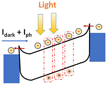 |
| Photogating effect | The photogating effect is a special case of the photoconductivity effect. When electrons or holes generated under light illumination are captured via the trapped states of the semiconductor, the carrier lifetime increases, because the detrapping process takes time for the formation of a high gain. | 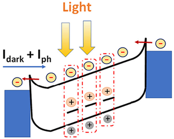 |
| Photovoltaic effect | The photogenerated e-h pairs are separated via the built-in electric field formed at a p-n or Schottky junction. |  |
| Photothermoelectric effect | The photothermoelectric effect occurs when the spot size of the laser used is smaller than the device size; a temperature gradient is generated at the channel, which can produce a photothermoelectric voltage and drive the current through the device without external bias. |  |
Reproduced with permission from ref [66]. Copyright 2022 Elsevier.
3. Strategies for Improving Performance of PDs
It is well known that the functions of materials are determined by their structures, including dimensions, composition, and crystal defects or atomic arrangements; therefore, structural modification of pristine 2D MoS2 is an important way to achieve better performance of 2D MoS2-based PDs [12]. In this section, we focus on electronic band structures and optical properties of 2D MoS2-based nanocomposites for PDs. Our highlights are to summarize some typical methods for regulating the structures of 2D MoS2 through surface/interface functionalization to improve the optical detection performance. These methods are essentially to modulate the R, τ, and light response range of 2D MoS2. For example, its optical absorption range can be regulated through defect engineering or surface functionalization with optical gain molecules. These approaches can mitigate the negative effect (e.g., lowering electronic conductance) of intrinsic structural defects (e.g., sulfur vacancies), and enhance light absorption [28,29].
3.1. Improving Photoresponsivity
The optical response of PDs based on pristine 2D MoS2 is limited due to small light absorption intensity. As shown in Figure 2, the introduction of light sensitizers (plasmonic metal), optical waveguide, reflection architecture, and optical resonance cavity, have been utilized to improve the optical properties of pristine 2D MoS2. Light sensitizers mainly include semiconductor sensitizers (e.g., quantum dots, QDs) [67,68,69], molecular sensitizers (e.g., organic dye molecules) [30,70], and plasmonic metal (e.g., gold and silver) NMs. Relatively, using an appropriate incident photon frequency, plasmonic metals can exhibit greater absorption cross sections due to localized surface plasmon resonance (LSPR), than that of semiconductor and molecular sensitizers [71].
The incident light is gathered by light sensitizers, which increase the light absorption range and strength of 2D MoS2. Light-generated electrons or holes produced by sensitizers are injected into conduction bands or valence bands of 2D MoS2 for the subsequent separation and transport [72]. In general, three mechanisms are reasonable to explain the improved performances of PDs based on the hybrid system composed of plasmonic metals and 2D MoS2 [73]. The first mechanism is that surface plasmons (SP) of metallic NMs as antennas for trapping light can improve the light absorption of surrounding semiconductors, resulting in the formation of more carriers. The second mechanism is that an enhanced electromagnetic field of the metallic nanostructures can be induced, which can promote the generation and separation of the e-h pairs in semiconductors. The third mechanism involves the decay of SP, which generates hot electrons injecting into the conduction bands of the surrounding semiconductors, and result in higher R beyond the limit of bandgaps [25]. Therefore, combining 2D MoS2 with plasmonic metal nanostructures to generate strong localized surface plasmon resonance (LSPR) is an effective method for enhancing the optical response (Figure 2), and the SPR at the nanoscale level is called as LSPR [74,75].
The LSPR effect of plasmonic metal nanostructures (e.g., nanoparticles, NPs) is dependent on their components, shapes, micro-environments (or substrate effects), and distribution states (e.g., periodic arrays). These factors determine the width and position of the LSPR band, the light-excitation efficiency of plasmonic nanostructures for energy transfer, and the optical properties for electric-field enhancement [73,76,77,78]. The components or types of plasmonic metal NPs can change the R of PDs. For example, compared with single-component metals, metal alloys can significantly improve the R of 2D MoS2 and other optical properties. Therefore, the inter-band transition of metal alloys can be flexibly adjusted for enhancing the surface plasmon-exciton properties via changing the ratio between alloying elements [79,80,81]. Some special shapes (e.g., sharp tips and tiny gaps) can effectively enhance the electromagnetic field strength of the LSPR, and thus greatly enhance the light-matter interaction [73,82]. For example, near-field amplification, scattering, exciton dephasing, and chemical interface damping are influenced by the geometry of specific metal NPs. In general, the decreased aspect ratio of metal NPs can result in a sharp decrease in the resonance intensity due to the increased damping rate of radiative plasmons in narrower NPs. In contrast, the NPs with high aspect ratios can exhibit higher SPR intensities, providing a strong near-field enhancement in the interstitial region [73,83,84]. Therefore, tuning the morphology (such as shape, size or distribution) of the metal NPs can change the resonance frequency and intensity of LSPR. For example, with increasing sphere diameter of monodisperse platinum (Pt) nanospheres from 29 nm to 107 nm, the LSPR resonance peak (the extinction peak) shifts to larger wavelengths (λ=248 nm for 29-nm-diameter particles and λ=494 nm for 107-nm-diameter particles) [85]. Raspberry-shaped Au NPs exhibit plasmon coupling that causes both red-shifting (from 550 to 600 nm) and a large broadening of the plasmonic resonance, compared to the signal from spherical Au NPs [86]. The distribution of metal NPs can affect the LSPR mainly via interparticle spacing. Collective plasmon modes of Au nanoparticle coverage area ratios of 10%, 37%, 71%, and 85% display red-shifted from 571 nm to 704 nm [87].In addition to pure metal nanomaterials, Cu2-xM (M = Se, S), heavily-doped metal oxides, and oxygen-deficient metal oxides can exhibit significant SPR [88,89]. However, to the best of our knowledge, their plasmonic properties are rarely used in 2D MoS2-based PDs.
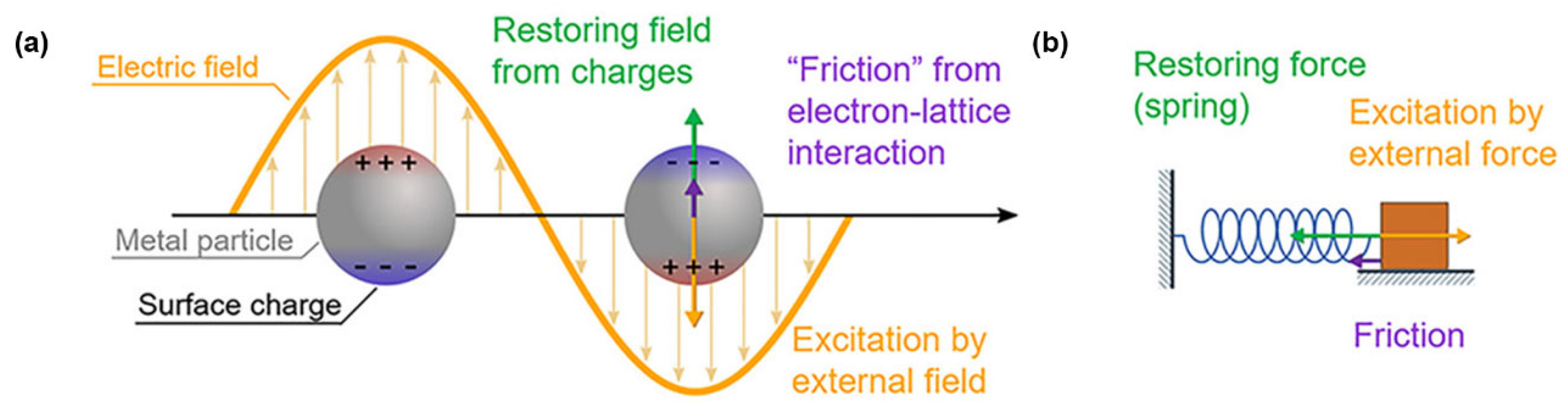
Metal plasmonic structure dynamics. (a) Electron behavior in a plasmonic NP under solar illumination. (b) A mechanical harmonic oscillator is used to explain the coherent electronic cloud on the metal surface under light forces. Reproduced with permission from ref [74]. Copyright 2019, American Chemical Society.
Metal plasmonic structure dynamics. (a) Electron behavior in a plasmonic NP under solar illumination. (b) A mechanical harmonic oscillator is used to explain the coherent electronic cloud on the metal surface under light forces. Reproduced with permission from ref [74]. Copyright 2019, American Chemical Society.
Another strategy for achieving an enhanced optical response is the integration of 2D MoS2 with optical waveguides or optical fibers so that the light fields can be confined in quasi-one-dimensional waveguide structures, and form a resonant state [90]. The optical waveguides allow absorption of evanescent light propagating parallel to the 2D MoS2. The light-matter interaction length is governed via the device length, rather than the layer thickness of 2D MoS2 [91]. Therefore, it is possible to design the interaction length to be sufficiently long to achieve strong optical absorption for the excitation of e-h pairs [92].
Light waves can be confined in both the space and time domains via a microstructure known as the optical resonance cavity for the manipulation of light at the nanoscale, which provides a standing wave cavity resonance for enhancing optical quantum efficiency. Such cavities can lead to strong light-matter interaction, and are frequently employed in optoelectronic devices and photonic-integrated circuits. In general, three types of optical resonance cavities (Figure 3) have been used in PDs, including: a) Fabry-Perot type cavities, b) 2D photonic crystal cavities, and c) whispering gallery mode microcavities [92].
3.2. Reducing Response Time
Generally, the τ of 2D MoS2-based PDs can be affected by the carrier lifetime because trapped states caused by inherent defects in the semiconductor and ambient gas absorption play an important role in prolonging the lifetime of the photo-excited carriers. These factors strongly affect the τ and the decay time of PDs. The PDs based on pristine 2D MoS2 generally exhibit sluggish R, and their τ is affected by the carrier lifetime, which is associated with structural defects. These defects are determined by synthesis processes and ambient gas absorption during the use of PDs. As a result, interface/surface passivation and encapsulation, such as the surface modification with organic dye molecules, can suppress charge Coulomb scattering and enhance carrier mobility for improving the performance of 2D MoS2-based PDs [93].
The influences of defects on the behavior of charge carriers are derived from the presence of charge traps (gap states or defect states), including hole and electron traps as well as “shallow” and “deep” traps (different energy positions), which are dependent on the type and concentration of charge traps. For example, they possibly extend the recombination time of photoinduced charge carriers or not. After the electrons in the conduction band are trapped by shallow traps, they return to the conduction band through thermal activation and recombine with the trap centers. When deep traps are formed in 2D MoS2, the probability becomes quite low for the electrons stored in the deep traps crossing the energy barrier and leaving the traps, and thus the electrons can remain metastable for a long time. However, only under strong excitation (e.g., light excitation or high temperature for thermal activation), can the electrons obtain enough energy and escape from the traps, and then recombine with the trap centers [94,95]. The deep hole traps require more energy to release holes to the valence band for the recombination of photo-generated e-h pairs. This process requires more time, which results in an increase of τ [96].
Intrinsic defects (e.g., S or Mo vacancies) in 2D MoS2 can usually lead to the formation of deep trap states, and thus prolong the lifetime of photoexcited carriers, which can affect the τ of PDs based on defective 2D MoS2. Under light illumination, the defect-induced deep trap states can extend the separation time of charge carriers, resulting in additional τ of PDs compared with shallow traps. The recombination rate of charge carriers and the formation of shallow traps, as two main factors, can strongly affect the decay time of PDs compared with deep traps [97]. Generally, defect passivation can be used to convert the deep-level defect state into the shallow-level defect state [98,99,100,101,102]. Defect passivation can occur through the absorption of O2 and H2O molecules on the defective sites (e.g., S vacancies) of 2D MoS2, and can lead to a sluggish photoresponse or a long decay time, compared to that in vacuum (Figure 4a). The adsorbed gas molecules as long-lasting charge traps can prevent the transport of carriers. However, this situation can be improved via encapsulation in high vacuum or passivation, such as adding a methylamine (MA) halide (MA3Bi2Br9) layer on 2D MoS2 (Figure 4b). Consequently, MA3Bi2Br9-MoS2 PDs exhibit faster τ and more stable photoresponse than those of pristine 2D MoS2 PD (Figure 4b) [103]. This is due to the presence of MA3Bi2Br9 as a passivation layer which leads to a reduced concentration of S-vacancies and deep traps (Figure 4c) [103].
3.3. Expanding Spectral Range
The photodetection ranges of PDs based on semiconductors are governed by their bandgaps, which are associated with the cutoff wavelength limit (or bandgap spectral limit) [104]. In general, the construction of broadband PDs (such as mid-IR and far-IR PDs) based on narrow-bandgap semiconductors is still full of challenges due to their large dark currents [105]. Therefore, the band-gap tailoring of 2D MoS2 is the focus of the following section. We will summarize the typical strategies, including the control over the thickness of 2D MoS2, defect engineering, and strain engineering [106,107,108,109], to achieve a wider response range.
Due to the quantum confinement effect, the band structure of 2D MoS2 displays a layer-dependent feature. When its thickness is reduced from bulk to a one-layer forms, its band gap can shift from 1.2 to 1.8 eV at the K-point of the Brillouin zone with a transition from being an indirect to a direct band gap semiconductor [110]. In addition, its charge carrier mobility is drastically reduced due to phonon scattering (Figure 5) [111,112,113]. PDs based on monolayer MoS2 can only cover the visible spectrum. This limitation severely restricts their use in broadband applications [29,114]. Fortunately, the electronic structure of 2D MoS2, including the bandgap and density of states (DOS), can be flexibly modified via defect engineering and strain engineering to acquire several unique features [115,116,117,118].
In addition to thickness control, the formation of additional structural defects is another efficient way to modulate the bandgap of 2D MoS2 for achieving to a broadband response [65,119,120]. The introduction of structural defects can reduce the orbital splitting between bonding and antibonding orbitals, and form new gap-states [72,121,122]. The gap-states are beneficial for the photoexcitation of charge carriers. The reduced bandgap facilitates the transitions from defect states to the conduction band or from the valence band to defect states, thus widening the light absorption range [72,123,124]. For example, MoS1.89-based PDs (containing rich S-vacancies) can allow the photodetection of mid-infrared light, while MoS2.15-based PDs (containing rich Mo-vacancies) can be used for detecting a longer wavelength due to the formation of S-vacancies or Mo vacancies [119].
In addition to vacancy engineering, strain engineering has been frequently used to construct broadband PDs, primarily by decreasing the bandgap of 2D nanomaterials, thereby increasing the maximum allowable absorption wavelength [29,125,126,127,128,129]. In general, strain engineering of 2D MoS2 can be realized mainly by the modulation of lattice structure and symmetry, which are dependent on the synthesis methods [127]. For example, 2D MoS2 with defect-free and single crystalline structure synthesized via chemical vapor deposition (CVD) is capable of withstanding nearly 5.6% and 1.98% biaxial strain (0º and 90º), which is much higher than that of traditional semiconductors [130]. Structural strain can be introduced through various methods, mainly including thermal and lattice ripples, substrate interactions, chemical doping, and mechanical bending or stretching (the localized uniaxial strain in 2D MoS2 is shown in Figure 6a-c) [131,132]. Based on the principle of buckling-induced delamination, 2D MoS2 flakes with well-aligned wrinkles can be synthesized by a four-step method (Figure 6a). The extent or morphology of wrinkles is dependent on the layer thickness (Figure 6b and Figure 6c), which can affect the optical properties (Figure 6d). These include exciton behaviors (e.g., trapping, dissociation, and binding) and carrier transport as well as band structures near the K point via regulating in-plane orbital interactions of 2D MoS2 (Figure 6e). As the strain increases, the PL peak of 2D MoS2 flakes exhibits redshift (Figure 6d), indicating a decrease in the bandgap and an expansion of the absorption spectral range of MoS2 (Figure 6e) [131]. Therefore, introducing tensile strain (e.g., wrinkles) can regulate the performance (e.g., R and spectral range of photodetection) of PDs based on pristine 2D MoS2, overcoming its fundamental absorption limit determined by the bandgap [114,133]. In addition, the optical cutoff wavelength of 2D MoS2 can be shifted from the visible range to the NIR region after applying tensile strain, particularly biaxial tensile strain [114].
4. Applications
Different surface or interface conditions of 2D MoS2-based photoactive materials have profound influences on their optical absorption and photocurrent generation. Surface and/or interface engineering performed via the combination of 2D MoS2 and 0D, 1D, or 2D NMs to form various of heterostructures can be used to manipulate light-matter interactions for high-performance PDs [134]. These NMs may act as transport channels on the surface of 2D MoS2, allowing for the capture and confinement of abundant photons, thus enhancing light absorption [28]. Compared with pristine 2D MoS2, PDs based on 2D MoS2-based heterostructures can exhibit enhanced R and τ due to the synergetic effects of 2D MoS2 and other components [135,136]. In the following parts, we will discuss recent developments of PDs based on 2D MoS2 after simple functionalization (e.g., elemental doping and conjunction with dye or inorganic sensitizers) and 2D MoS2-based hybrid heterostructures covering 0D/2D, 1D/2D, 2D/2D, and other mix-dimensional heterostructures.
4.1. PDs Based on 2D MoS2 After Simple Functionalization
For PDs based on pristine 2D MoS2, there are some problems including the weak absorptivity of incident light (5-10%) [137], low detectivity, large dark current, and small light on/off ratio [138]. Suitable elemental doping, defect engineering based on optimized surface treatments, and strain engineering have been used for the surface modification and functionalization of pristine 2D MoS2 to improve the performance of PDs (as shown in Table 2).
The main reason for using elemental (e.g., N, W, and Sn) doping is to regulate the carrier concentration and bandgap, which can affect the injection and separation efficiency of carriers, thus improving PD performance (e.g., R). For example, 2D MoS2 is grown on the W-implanted SiO2 substrates by CVD to achieve W-doped MoS2 and avoid the damage caused by direct ion implantation. W-doping results in a widened bandgap and a higher hole concentration of 2D MoS2 so that the PD based on W-doping 2D MoS2 exhibits a faster τ than that on pristine 2D MoS2 [139]. Similarly, Sn-doped 2D MoS2 flakes (at Mo sites for the formation of Sn-Mo-S bonds) through ion implantation are used to control Sn concentration in MoS2, thereby enhancing photodetection ability compared to pristine MoS2 flakes. The reason is that the introduction of Sn can enhance the transfer of photogenerated electron by providing a lower energy barrier [140].
Introducing imperfections into the atomic lattices and strain engineering can be applied to 2D MoS2 to alter the electronic and optical properties for achieving a broadband response. Different defect concentrations or rates of Mo vs. S in 2D MoS2 produce varied bandgaps (Figure 7a). The smaller the bandgap, the larger the fluctuation of carrier concentration, which enables efficient photodetection beyond the intrinsic bandgap-limited wavelength response range. By employing pulsed laser deposition (PLD) to introduce Mo defects or S defects, the tunneling electrons are transferred from 2D MoS2 to the metal surface without external THz radiation (Figure 7b). When an antisymmetric electric field is formed via applying external THz radiation, the energy of electrons in the Au metal increases, and the energy barriers against electron transfer are shifted downward (Figure 7c). Before and after applying THz radiation, the direction of interface electron transport between 2D MoSx and Au electrodes via interband transitions will be changed due to the presence of light driving force. The presence of S or Mo defects (vacancies) in 2D MoSx can form the quantum wells of carriers, and thus can enhance the ability of accumulating the charge carriers (Figure 7d). Under the THz radiation, more electrons transfer from the Au electrodes to the defective MoS2 surface until reaching the equilibrium states between electron field and light driving force (Figure 7e). Photodetection performances show that the influences of the applying bias on the resistivity and R are similar, namely, the large bias can lead to the high R and resistivity (Figure 7f) [141].
Introducing S defects in the crystal lattice of 2D MoS2 can control the element ratio of S vs. Mo with the PLD technique. Defect engineering can reduce the band gap, allowing PD based on defective 2D MoS2 with rich S-vacancies to exhibit an ultra-broadband photoresponse across a spectrum ranging from 445 to 2717 nm. For example, the PDs based on 2D MoS1.89 display high detectivity and a broadband photo-response from visible to mid-infrared light [119]. Of note, the defect states of 2D MoS2 are associated with its synthesis methods, such as mechanically exfoliated (ME) methods [142,143], chemically-exfoliated methods [113], sputtering method [144], and CVD [145,146,147], which can ultimately affect the performance of PDs. For example, a phototransistor based on single-layer MoS2 obtained via the ME method was constructed and displayed a better R than that of a graphene-based PD with a large dark current. When the drain or gate voltage is kept constant, the photocurrent of this phototransistor is determined by the applied light intensity [148]. In addition to S-vacancies, the induced strain in 2D MoS2 is another useful strategy for regulating the band structure for an ultra-broadband MoS2 PD because of its control over the optical properties. As shown in Figure 8a, a PD based on monolayer MoS2 obtained via mechanical exfoliation and placed onto a polymeric substrate (e.g., polycarbonate, PC), exhibits better biaxial strain (tensile or compressive) expansion with the change of temperature (Figure 8b) than that of 2D MoS2. This phenomenon is attributed to the reduced band gap, which can be proved by the red shift of A and B exciton resonance peaks (Figure 8c). By optimizing the level of strain, a high R can be obtained even under relatively low illumination intensity due to the formation of long-lived charge trapping for charge separation [149].
Table 2.
Summary of various PDs based on 2D MoS2 after simple functionalization.
| Architecture | Main synthesis method | R (A·W-1) | τ | D(Jones) | Wavelength (nm) | Ref. |
| MoS2 | PLD | 50.7 × 10⁻³ | - | 1.55 × 10⁹ | 445-2717 | [119] |
| MoS2 | ME | 7.5 × 10⁻³ | 50 ms | - | - | [148] |
| MoS2 | CVD | 11.1 | 7.7 ms | 5.4 × 10¹³ | 660 | [150] |
| MoS2 | ME | 59 | 42 μs | - | 532 | [151] |
| MoS2 | Hydrothermal | 2.33 | - | - | 375-915 | [152] |
| MoS2 | ME | 2.67 × 10⁶ | 5 ms | - | Vis-NIR | [38] |
| MoS2 | Ultraviolet lithography technology | 104 | - | 2 × 10¹² | 532 | [153] |
D: detectivity; PLD: pulsed laser deposition; ME: mechanically exfoliated; τ: response time; NIR: near-infrared; Vis: visible; - The data are not available.
4.2. PDs Based on 2D MoS2-Based Nanocomposites
Although PDs based on 2D MoS2 after simple treatments (e.g., the introduction of S-vacancies) have already achieved excellent performances, it is necessary to further improve their performance for some applications. Heterostructure engineering (as shown in Figure 9) based on the integration of 2D MoS2 and other low-dimensional NMs, such as 0D nanoparticles and 1D nanowires (NWs), is another promising strategy for combining the fascinating properties of different materials and overcoming the shortages. Therefore, it is quite flexible in controlling the light-matter interactions at the nanoscale level and regulating the optical properties of 2D MoS2 for constructing high-performance PDs. Among PDs, the photoconductive-type sensors (as shown in Table 3) based on MoS2-based nanocomposites have been widely used to detect various environmental pollutants such as Cu2+, Hg2+, and Escherichia. Such environmental monitoring data obtained via these PDs can lay the foundation for the development of systemic environmental monitoring and indicators for sustainability. In this Section, we will discuss recent processes of 2D MoS2-based heterostructures for constructing high-performance PDs [28].
4.2.1. 0D NM-Modified 2D MoS2
0D metal NMs, and semiconductor or semimetal QDs (Table 4), are widely utilized to enhance light absorption, separate photoinduced charge carriers, and control field polarization for modifying 2D MoS2 for high-performance PDs due to the synergetic effects of these components [163]. For example, the 0D/2D mixed-dimensional heterostructure for PDs will exhibit a higher R and a lower dark current than those of pure individual materials. This is mainly due to the special interface properties and optical resonance absorption of electrons in conduction band of 0D NMs in response to the incident light [164,165,166]. High photocarrier mobility is usually provided by 2D materials, while increased light-matter interaction is realized by 0D materials with controllable optical characteristics. In this case, 0D plasmonic metal NMs are periodically or randomly distributed on the basal planes of 2D MoS2 for regulating the optical properties of 2D MoS2 due to the LSPR effects in confined geometries (Figure 9a).
In the hybrid system, the LSPR features of 0D metal NMs with different components and shapes can enhance local field intensity at their junctions, and overcome the optical diffraction limit (e.g., light absorption) of the traditional semiconductors nearby, which is determined by their band gaps. For example, sparsely deposited Au NPs on 2D MoS2 for constructing PDs exhibit an obvious increase in the photocurrent response, near-field oscillation, and scattering effects, because of the LSPR of Au NPs. Additionally, the presence of Au NPs as acceptors can enhance light trapping and absorption via surface energy transfer from Au NPs to 2D MoS2, which can further improve carrier separation rate [167]. The photocurrent of periodic Au-nanoarray/2D-MoS2 nanocomposites exhibits a threefold enhancement than that of pristine 2D-MoS2 phototransistors (without Au NPs), because the periodic NPs arrangement can enhance the local electric field (antenna field enhancement), thus further promoting carrier generation and separation [168]. This phenomenon is more pronounced in periodic Au nanoarrays than sparse Au NPs, when they are deposited on 2D MoS2 for constructing phototransistors. In the hybrid system of a periodic metal nanoarray modified with 2D MoS2, Au NPs enhance scattering and the optical range length inside the 2D MoS2. As a result, they trap light more efficiently and enhance light absorption of the nearby 2D MoS2. Metallic NPs placed at a short distance induce near-field interactions or dipolar interactions. Consequently, the different gap sizes between metallic NPs affect their plasmonic properties [169].
Large-area Au-NP gratings with two sets of diameters and densities (Figure 10a) were synthesized using a combination of traditional photolithography with thermal annealing. The NP grating structures show a large degree of enhancement in extinction spectra (Figure 10b) and photocurrent (Figure 10c), and their light absorption under 532 nm illumination is stronger than that of the single-size NP array, which can be attributed to the LSPR effect and the carrier-multiplication effect of light generation [170]. In addition, modulating the size distribution and changing the structural stacking order are other strategies used to improve the performance of PDs. For example, the sandwich like structures (Figure 10d) of Au-MoS2-Au nanocomposites obtained through the ME method show a significant enhancement in R (1757 A·W-1), which is almost three times higher than that of Au-MoS2 nanocomposites, upon 532 nm irradiation (Figure 10e). The Au-MoS2-Au arrangement can generate more hot electrons, which readily overcome the interface barrier between Au NPs and 2D MoS2, and inject into the conduction band of 2D MoS2. Therefore, the photocurrent is improved when the incoming light frequency is close to the LSPR frequency of Au NPs (Figure 10f). Meanwhile, under the same illuminating situations, Au NPs on the basal planes can produce strong local electric fields (Figure 10g) and exhibit a rapid response to turning light on or off (Figure 10h). There is also an increased plasmonic scattering effect (Figure 10i), which leads to a high R and a low decay time [171].
In addition to the LSPR effect, the thermal effect of the plasmonic nanostructures is attributed to the collective oscillations and collisions of conduction electrons. It can be fine-tuned by varying external irradiation and also makes a significant contribution to the photocurrent enhancement by increasing electron temperature, which activates electrons to high-energy states. This is similar to pyro-catalysis, where waste energy is harvested [172]. The thermal effect is ascribed to collisions between non-equilibrium hot electrons and phonons or other quasiparticles. For example, a strain-plasmonic coupled PD by mechanically integrating a single layer MoS2 with a tensile strain onto a pre-fabricated Au NP array as thermo-plasmonic nanostructures, can widen the photodetection range due to the enhanced light absorption and the local thermal effect. The reduced band gap of 2D MoS2 results from the introduction of structural strain and the LSPR effect of Au NPs. The strain-plasmonic coupling effects lead to the broadband photoelectric detection [29]. In addition, the nanoscale interface formation in 0D-2D hybrid systems and the strong light-sensitive absorption of 0D NMs can enhance photodetection performance. Similarly, 0D CdSe/ZnS QDs, as a charge source to form excitons and transfer e-h pairs, are combined with 2D MoS2 to improve the separation efficiency of these pairs due to the formation of nanoscale interface. As a result, the 0D CdSe/ZnS QDs /MoS2 hybrid van der Waals (vdW) heterojunctions exhibit the enhanced photoresponses and detectivities [173].
In addition to metal NMs, QDs are commonly used for modifying 2D MoS2, because they display some attractive features such as facile bandgap tunability, large area manufacturability, adjustable size, and flexible synthesis methods. These can be used for regulating the photodetection activity of 2D MoS2 [174,175]. In particular, some MXene QDs and PbSe colloidal quantum dots (CQDs) exhibit the LSPR effect, which can concentrates incident lights [29,168,169,170,175,176]. For example, plasmonic nanocomposites consisting of MXene QDs (average size of ~ 8 nm) and 2D MoS2 were synthesized using simple CVD and spin-coating methods (Figure 11a). Compared to the pristine 2D MoS2, the PD based on the hybrid plasmonic structure (MXene-QD/2D-MoS2) exhibits a lower dark current (Figure 11b), a higher photocurrent (Figure 11c and Figure 11d), and a faster photoresponse under the same light illumination. These properties are ascribed to the fast electron diffusion and separation from 2D MoS2 to the MXene, as well as the LSPR effect of MXene QDs, which can enhance light absorption. In addition, the LSPR effect facilitates the interaction between the light and the localized electric field [176].
The combination of 0D semiconductor QDs with 2D MoS2 as a substrate can significantly improve the total PD performance, which is attributed to the improved dispersion and stability of QDs. The fast interfacial charge transfer in this substrate can overcome carrier recombination. Semiconductor QDs synthesized via wet chemical methods exhibit versatile surface properties and efficient light harvesting ability. In particular, CQDs are considered a promising class of building blocks for next-generation PDs due to their simple solution processing, tunable bandgap, excellent light harvesting, low-cost fabrication, size-tunable optoelectronic features, and flexibility [177]. Integrating 2D MoS2 with CQDs can improve carrier mobility. For example, a hybrid structure composed of 2D MoS2 and PbSe CQDs for constructing a PD can extend its sensitivity towards the mid-infrared range. Due to effective carrier separation at the interface between 2D MoS2 and PbSe CQDs, the dark current is decreased. In this case, the PD can be performed at RT with R of 137.6 A·W-1 and a detectivity of 7.7 × 10¹⁰ Jones at 2.55 μm [175]. The human body is sensitive to ultraviolet radiation, which can lead to different types of diseases, including cataracts and skin cancer. Therefore, it is essential to develop modern and efficient UV PDs [178]. The combination of UV-sensitive SnS2 QDs and 2D MoS2 (Figure 12a) can simultaneously extend the response range and enhance the R. Thereinto, the monolayer MoS2 deposited on the substrate of SiO2/Si by CVD and combined with SnS2 QDs by a solution processing method would be useful. The charge-carrier injection and separation efficiency are enhanced due to the interface band bending and the formation of a built-in electric field (Figure 12b). Although monolayered MoS2 is sensitive to Vis-NIR radiation, the introduction of SnS2 QDs to form vdW heterostructure allows the UV spectral absorption, and thus allowing the device to work in the UV-vis-NIR photoresponsive range (Figure 12c). At the same time, the dark currents can be efficiently suppressed, because of high separation rate of charge carriers. The PD device based on the heterostructure of SnS2 QDs and 2D MoS2 achieves R of ∼278, ∼435, and ∼189 A·W-1 in the UV, Vis, and IR, respectively [174].
Table 4.
Summary of various PDs based on 0D NM-modified 2D MoS2.
| Architecture | Main synthesis method | R (A·W-1) | τ | D (Jones) | Wavelength (nm) | Ref. |
| Au/MoS2 | ME | 186.6 | 1.8 ms | 1.41 × 10¹² | Vis | [179] |
| Au/MoS2 | Magnetron sputtering, thermal annealing | 38.57 | - | 9.89 × 10⁹ | Vis | [170] |
| MXene NPs/MoS2 | CVD | 20.67 | - | 5.39 × 10¹² | - | [176] |
| Au-MoS2-Au | ME | 1757 | 24 ms | 3.44 × 10¹⁰ | - | [171] |
| SnS2 QDs/MoS2 | CVD, spin coating | 435 | 0.1 s | 7.19 × 10¹² | Vis | [174] |
| PbSe CQD/MoS2 | ME and spin coating | 137.6 | 0.04 s | 7.7 × 10¹⁰ | IR | [175] |
D: detectivity; CQD: colloidal quantum dots; QDs: quantum dots; CVD: chemical vapor deposition; ME: mechanically exfoliated; τ: response time; IR: infrared; Vis: visible; - The data are not available.
4.2.2. 1D NM-Modified 2D MoS2
In general, 1D NMs exhibit some superior physical and chemical properties such as quantum confined transport and anisotropic properties, which allow their optical absorption and carrier mobility to be flexibly regulated. Multiple morphologies of 1D NMs (Table 5), such as NWs, nanotubes (NTs), and nanorods (NRs), serve as excellent optical absorbers or antennas and flexible combination with 2D MoS2 for the formation of various of heterogeneous structures (Table 5). In addition, their interfacial coupling of 1D NMs/2D MoS2 can obtain the synergistic advantages in the performance of PDs [180,181,182].
Most nanostructure-based PDs are designed to be powered by an external power source used to stimulate the generation of photogenerated charge carriers. This can lead to the increase in the size and weight of the devices. As a result, their applications in fields such as in situ medical monitoring and wireless environmental sensing, are severely restricted. The self-driven PDs based on the photoelectric effect of p-n junctions is an important research direction for the next generation of nano-devices. The p-n lateral heterojunctions composed of 2D MoS2 nanoflakes (n-type) modified via 1D GaAsSb NWs (p-type) were obtained using mechanical exfoliation method and CVD process. The heterojunctions with type-II interfaces exhibit desirable properties (such as anti-ambipolar behavior), which are useful for constructing phototransistor devices. Compared to pristine 2D MoS2, the heterojunctions exhibit enhanced photodetection performance. This improvement is attributed to the introduction of p-n semiconductors in channel materials, which can improve carrier concentration and decrease recombination rate. Moreover, the photodetection performance of this heterojunction phototransistor can be readily regulated via its external gate [180]. Similarly, 1D-ZnO-NW/2D-MoS2 p-n heterostructures for PDs exhibit a fast response to the wide electromagnetic spectrum and increased R, compared to that of PDs based on 2D MoS2. The phenomena are attributed to the special carrier behavior (Figure 13) that electrons in ZnO NWs migrate to 2D MoS2, while holes move from 2D MoS2 to ZnO NWs. As a result, the photogenerated carriers are rapidly separated and then transferred to the electrode for generating a photocurrent, which leads to the fast reaction rate and improved transient response and responsivity in 1D-ZnO/2D-MoS2 PDs [182].
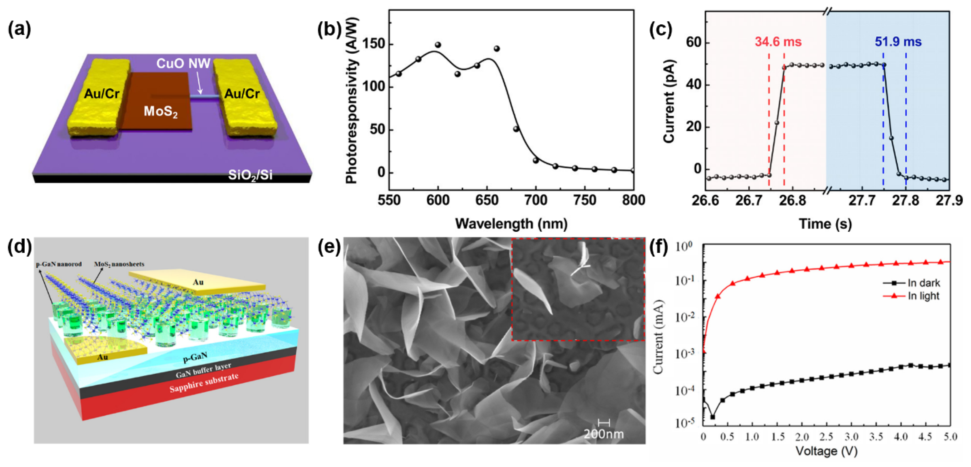
As a p-type semiconductor, CuO NWs have varying band gaps (including direct bandgap or indirect bandgap) in the range of 1-4.5 eV, which are dependent on the atomic arrangements [183]. Therefore, CuO NWs can exhibit a high and tunable photoresponse to light illumination ranging from UV to NIR region via bandgap engineering. This offers possibilities for constructing high-performance PDs when combined with 2D MoS2. For example, a high-performance PD was developed based on MoS2 nanosheets modified on CuO NWs (Figure 14a), which were synthesized via mechanical exfoliation and wet-transfer printing. The R of this PD is dependent on the laser wavelength, which shows two strong absorption peaks (Figure 14b) and a high R of 157.6 A·W-1 due to the presence of the trap states. Under Vis-NIR incident light illumination, the heterostructure PD can exhibit a low dark current and a quick τ due to the high separation rate of charge carrier pairs (Figure 14c) [184]. Similarly, 1D Si NW array (Si NWA) as an active layer can enhance light harvesting and improve quantum efficiencies of 2D MoS2. Therefore, PDs based on the vertical 1D/2D heterostructure composed of 2D MoS2 and 1D Si NWA can exhibit high gain and R. The Si NWA/2D MoS2 heterostructure was synthesized by placing an MoS2 film onto the top of vertically ordered Si NWA obtained through Ag-assisted chemical etching of n-type Si wafers. The Si NWA/2D MoS2 heterostructure PD exhibits high performance across the UV-NIR spectrum, mainly because of light-trapping abilities of Si NWA and the formation of a built-in electric field, which can accelerate the charge carrier transfer and separation from 2D MoS2 to Si NWA. This PD device exhibits an on/off ratio of up to 105 and a low noise current, and it even can detect weak IR signals [138].
Compared with Si NWs, one of the most obvious advantages of 1D transition metal oxides, such as V2O5 NWs, is their better stability. Therefore, the hybrid 1D/2D heterostructure composed of V2O5 NWs and 2D MoS2 for PDs, not only exhibits broadband sensitivity from UV to NIR but also offers improved stability. For example, V2O5 NWs were synthesized by electrospinning, and combined with hydrothermally prepared 2D MoS2 films using spin-coating. The heterostructure can enhance the separation of photoinduced charge carriers. In addition, the introduction of V2O5 NWs onto 2D MoS2 nanosheets is beneficial for the light adsorption and photogenerated carrier generation. The broadband PD can be constructed based on the heterostructure and can detect UV-NIR radiation. This is because V2O5 NWs absorb UV-Vis light, while 2D MoS2 is responsible for Vis-NIR light absorption [185].
Gallium nitride (GaN), as a wide band gap semiconductor, is widely used in UV PD devices due to its wide bandgap of 3.44 eV, which enables high R and fast operation for UV photoresponse. Therefore, the combination of GaN and 2D MoS2 can cover the photodetection in the range of UV light, which is blind for 2D MoS2. For example, the 1D-GaN-NR/2D-MoS2 heterostructure was synthesized by growing 2D MoS2 nanosheets on GaN NRs as the substrate, using the PLD method. This heterostructure PD exhibits excellent performance with a broadband photodetection range of 300-1000 nm, a maximum response rate of ∼14.22 A·W-1, and a microsecond-level τ due to the high aspect ratio of NRs and widely exposed surface. The presence of vertical MoS2 nanosheets on the GaN substrate in this heterostructure is beneficial for improving light absorption and R [186]. Another heterostructure of 1D-GaN-NR/2D-MoS2 was synthesized using CVD method where vertical MoS2 nanosheets were grown on p-GaN NRs as a substrate to form heterogeneous structures (Figure 14d). The arrangement style of MoS2 nanosheets maximizes the exposure of edge sites (Figure 14e) so that an enlarged exchange current density can be obtained. The current-voltage curves (Figure 14f) of this PD in the dark and under laser illumination show that the dark current of the device is about 1 × 10⁻⁴ mA. This is much lower than the current of 1 × 10⁻¹ mA under illumination, demonstrating that the PD has a large optical gain. The 1D-GaN/2D-MoS2 heterostructure PD exhibits a fast photoresponse in a wide electromagnetic spectrum (500-750 nm), indicating that the vertical p-GaN/MoS2 heterostructure has promising applications in visible light devices [187].
Figure 14.
Schematic presentation of the device structure (a), plot of R vs. wavelength (b), plot of current vs. decay time (c) 2D-MoS2/1D-CuO heterojunction PD. Reproduced with permission from ref [184]. Copyright 2016 American Chemical Society. (d) Schematic diagram of the PD device based on vertical MoS2 nanosheets/p-GaN NRs. (e) SEM image of vertical MoS2 nanosheets. (f) The dark and illuminated I-V curves of the PD device. Reproduced with permission from ref [187]. Copyright 2019 American Chemical Society.
In addition to these semiconductor nanomaterials, carbon NTs (CNTs) are considered as idea active materials in optoelectronic fields due to their small diameter (1-3 nm), ballistic transport, high stability, and mobility. However, CNT PDs are not as effective as traditional semiconductors due to the impurities in CNTs. With the rapid development of techniques for CNT purification and surface modification, CNT-based PDs are becoming an increasingly important field of research. For example, a mechanically stable, highly responsive, and flexible PD was developed by integrating an all-carbon transistor with 2D MoS2. By combining the high mobility of single-walled CNTs (SWCNTs) with the light-matter interaction of 2D MoS2, this heterostructure PD can exhibit substantially better photoresponse than that of pristine SWCNTs or 2D MoS2 [188]. The PD based on SWCNT /MoS2 heterostructures that were synthesized via in situ chemical vapor deposition (CVD) of MoS2 on individual SWCNTs, exhibits high responsivity (100-1000 A·W−1) at low bias voltages (0.1 V) in the visible spectrum (500-700 nm) due to the high mobility channel of SWCNT, efficient light absorber of MoS2, and efficient charge transfer from MoS2 to SWCNT.
Table 5.
Summary of various PDs based on 1D NM-modified 2D MoS2.
| Architecture | Main synthesis method | R (A·W-1) | τ | D (Jones) | Wavelength (nm) | Ref. |
| ZnO/MoS2 | ME, annealing and spin coating | 24.62, 0.35 | 0.9 s, 140 ms | - | 365 nm,532 nm | [182] |
| CuO/MoS2 | ME, wet-transfer printing and spin-coating | 157.6 | 34.6/51.9 ms (rise/decay) | - | Vis | [184] |
| Si NWA/MoS2 | Thermal decomposition method, spin-coating, chemical etching method | 53.5 | 2.9/7.3 μs (rise/decay) | 2.8 × 10¹³ | UV-NIR | [138] |
| V2O5/MoS2 | Hydrothermal method, spin-coating | 6.51 × 10⁻² | - | - | UV-NIR | [185] |
| GaN/ MoS2 | Molecular beam epitaxy, PLD | 14.22 | 8.2 μs | - | 300-1000 nm | [186] |
| GaAsSb/MoS2 | CVD | 11.7 | 50 μs | 1.64 × 10¹¹ | 532 nm | [180] |
NWA: nanowire array; ME: mechanically exfoliated; D: detectivity; τ: response time; CVD: chemical vapor deposition; PLD: pulsed laser deposition; NIR: near-infrared; UV: ultraviolet; Vis: visible; - The data are not available.
4.2.3. 2D NM-Modified 2D MoS2
Graphene and some 2D semiconductors such as MoTe2, WS2, and GeSe, have been combined with 2D MoS2 to form superlattices or vdW heterostructures for constructing high-performance PDs (Table 6) [189,190]. The PDs exhibit high performance, such as low dark currents, high optical gain and R, due to their unique interfaces for the optimization of carrier lifetimes. The thinness of 2D MoS2 restricts its light absorption and carrier concentration. Therefore, the introduction of other 2D nanomaterials (e.g., cesium lead halides [191], GeSe [192], and WS2 [193]) as optical absorption antennas with extraordinary optoelectronic properties or as electron-transfer solid media (e.g., graphene [194]) for charge separation, is necessary for improving optical responses of 2D MoS2, such as the enhancements in photocurrent and quantum efficiency.
Various 2D crystals can be vertically stacked with 2D MoS2 by weak vdW forces, creating a wide range of possibilities for constructing high-performance PDs [195,196]. The properties of 2D/2D vertical heterostructures can be flexibly controlled by changing the layer number, order, and components in layer-by-layer assembly processes. This provides more degrees of freedom to manipulate photoelectric properties, because different 2D NMs exhibit varied band gaps, spin-orbit coupling strengths, and working functions [197,198,199]. In addition, the synthesis conditions of the vdW heterostructures are relatively simple, and do not require lattice matching for crystal growth. 2D MoS2 has a naturally passivated surface without any hanging bonds. Therefore, it avoids lattice mismatch problems when stacked with other 2D materials. The 2D/2D vdW heterointerface can exhibit special optoelectronic properties, such as outstanding electrical transport capabilities for photodetection. In addition, the built-in potential of the heterojunctions can reduce the dark current, efficiently separate the photo-generated e-h pairs, and enhance the efficiency of photon absorption [200,201]. Compared to PDs based on pristine MoS2 and other heterostructures (e.g., 0D/2D and 1D/2D), PDs based on 2D/2D heterostructures may exhibit higher performance due to better coupled interfaces and less trap states in their interfaces.
2D cesium lead halides (CsPbX3, X = Cl, Br, I) as functional materials for the modification of 2D MoS2 exhibit unique optoelectronic properties, such as high external quantum efficiency (> 90%) and strong stability. In addition, they display excitonic behavior similar to epitaxial quantum wells. Therefore, they can act as a common building block for PDs, especially as an ideal platform for the surface modification of 2D MoS2 for the high-performance vdW heterojunction PDs. For example, 2D MoS2 was synthesized via CVD and combined with 2D CsPbBr3 for the formation of high-quality CsPbBr3/MoS2 heterojunctions (Figure 15a). The Fermi level difference between MoS2 and CsPbBr3 creates a built-in electric field, which is beneficial for the separation of e-h pairs. The CsPbBr3/MoS2 heterojunction exhibits an enhanced separation rate of charge carriers (Figure 15b and Figure 15c) and improved light absorption (Figure 15d) due to the interfacial built-in electric field and the vertical stacking structure. The photoinduced e-h pairs formed on 2D CsPbBr3 are separated so that the holes are left in the valance band of 2D CsPbBr3, and the high-energy electrons are further transmitted to the conduction band of 2D MoS2 (Figure 15b). The formation of Schottky barrier can be beneficial from the carrier transport, which results in a higher photocurrent. The photocurrent and dark currents (Figure 15e) of the CsPbBr3/MoS2 PD are much higher than those of pristine 2D CsPbBr3 or MoS2. The main reason is that a high-quality interface of CsPbBr3/MoS2 improves carrier concentration and transport. The CsPbBr3/MoS2 PD exhibits superior photodetection capabilities with a high R = 4.4 A·W-1 and an external quantum efficiency (EQE) > 300% (Figure 15f) [191].
In addition to excellent electrical properties, graphene has some unique optical characteristics for PDs, such as a fast photoresponse and high bandwidth from visible to mid and far-infrared light. Therefore, single- and few-layer graphene can be used to produce broad-spectrum PDs by energy band gap modulation, because pristine graphene still faces some problems, such as low optical absorptivity [202,203]. The combination of graphene with 2D MoS2 is effective for modulating the optical properties of graphene. For example, the vdW heterojunction composed of p-type 2D MoS2 stacked on graphene was synthesized by CVD method. The Schottky barrier height of the vdW heterojunction can be flexibly regulated by back-gate bias for promoting carrier mobility and optical absorption [204,205]. In general, the Schottky photodiodes (Figure 16a) based on the graphene/MoS2 vdW heterojunction under different bias conditions exhibit a rectification effect for the case of forward bias and strong resistance for the case of reverse bias (Figure 16b). In addition, the photodiodes under forward bias exhibit better R than those under reverse or zero bias conditions [35]. The excitation of charge carriers includes energy gap excitation and internal photoemission, depending on factors such as incident-light energy, Schottky barrier height, and the band gap of 2D MoS2 stacked on graphene. The noise equivalent power of graphene/MoS2 measured is lower than that of a typical silicon PD due to the formation of Schottky junction (Figure 16c). In addition, graphene/MoS2 has excellent R over a broad wavelength range from Vis to NIR (Figure 16d), and the enhancement of R is determined by the photoconductivity of graphene (Figure 16e) [194].
In addition to the zero-gap graphene, some 2D semiconductors such as 2D MoTe2, WS2, black phosphorus, and GeSe, have been combined with 2D MoS2 for constructing wideband PDs with low tunneling dark current and improved optical gain and R. The reason is that 2D/2D vdW heterostructures exhibit intrinsic flexibility to precisely regulate optical properties. This can be readily realized by changing the layer stacking order, number, and components for further control over charge carrier behavior. These 2D-2D semiconductor heterostructures are usually synthesized via the ME and a restack technique (Table 6), and exhibit stable and excellent optoelectrical properties. For example, high-quality WS2/MoS2 vdW heterostructures were obtained using a two-step CVD process on SiO2/Si substrates. They act as active device materials for constructing broadband PDs due to the formation of a space charge region and interfacial built-in electric-field, which are beneficial for the separation of photo-induced e-h pairs, resulting in enhanced photocurrent and R as well as low dark current [193]. Additionally, a graded junction composed of p-type few-layer black phosphorus and monolayer MoS2 was synthesized using mechanical exfoliation and CVD. The materials were used for constructing broad-band photodiodes for the photodetection of mid-infrared radiation, because the p-n junction can enhance the optical absorption and suppress the dark current. The monolayer MoS2 as the cover can protect black phosphorus from oxidation, which can improve the stability of this PD.
Self-powered PDs based on vertically stacking 2D nanomaterials are attracting more research interest since they work at zero bias without applying an external power source. They can be classified into p–n junction, Schottky junction, and photoelectrochemical photodetection devices. Self-powered PDs based on 2D-2D vdW heterostructures exhibit high-photodetection performance with low energy consumption, thanks to the photovoltaic effect. This is because the 2D-2D vdW heterostructures can be beneficial for the efficient separation and transport processes of photo-generated carriers. More importantly, they can balance fast photo-response and high sensitivity due to the presence of interfacial built-in electrical field, which cannot be achieved in typical PDs. For example, a heterostructure of WSe2/MoS2/WSe2 was synthesized by mechanic exfoliation and transfer technique. This heterostructure was employed to construct self-powered PDs with a low dark current and high detectivity in the UV-NIR range due to the enhanced light absorption [206].
Additionally, GeSe/MoS2 p-n heterojunctions can be fabricated using a ME and a dry transfer method to construct a polarization-sensitive high-speed PD. This heterostructure based device is different from PDs based on SnSe/MoS2 and GaTe/MoS2 heterojunctions, which are not sensitive to the polarization states of light [207,208]. The p-n heterojunction PD displays a high R across a wide photodetection range, spanning from UV to mid-infrared. This is due to its type-II band alignment, which results in a high separation rate, long lifetime, and fast transport of charge carriers. The optical absorption of 2D GeSe is closely related to the atomic arrangement and orientation within the crystal, ensuring sensitivity to polarization states of incident light [192]. Vertically stacked p-n junction of p-MoS2/n-MoS2 for constructing phototransistors can efficiently enhance the separation of photo-excited carriers due to optimal band alignment and the formation of a built-in field. The concentration of charge carriers is significantly affected by the directions of applied bias, and thus can affect the responsivity of the phototransistors [209].
Table 6.
Summary of various PDs based on 2D NM-modified 2D MoS2.
| Architecture | Main synthesis method | R (A·W-1) | τ | D (Jones) | Spectral response |
Ref. |
| CsPbBr3/MoS2 | CVD | 4.40 | 0.72 ms | 2.5 × 10¹⁰ | - | [191] |
| Graphene/MoS2 | CVD | 1.26 | - | - | 1400 nm | [194] |
| WS2/MoS2 | CVD | 0.37 | 0.281/0.599 s (rise/decay) | - | Vis | [193] |
| P-GeSe/n-MoS2 | ME | 0.105 | 110/750 ms (rise/decay) | 1.03 × 10¹⁰ | 380-1064 nm | [192] |
| n-MoS2/p-GaN | Spin coating | 35.6 | 200 ms | - | Vis-UV | [210] |
| p-rGO/n-MoS2 | CVD | 2.10 | 18 ms | 5 × 10¹¹ | Vis | [211] |
| SiO2/MoS2 | ME | 4.05 × 10⁴ | 0.78/1.13 ms (rise/decay) | 3.32 × 10¹¹ | 447 to 1600 nm | [134] |
| Sb2O3/MoS2 | CVD | 5.3 × 10⁴ | < 60 ms | 2.0 × 10¹⁵ | Vis-NIR | [212] |
| PbSe/MoS2 | ME | 23.5 | - | 3.17 × 10¹⁰ | Vis-NIR | [213] |
| Cs2Pb(SCN)2Br2/MoS2 | CVD | 1.22 × 10⁵ | 166 ms | 1.16 × 10¹⁴ | Vis | [214] |
UV: ultraviolet; rGO: reduced graphene oxide; ME: mechanically exfoliated; D: detectivity; τ: response time; CVD: chemical vapor deposition; Vis: visible; - The data are not available.
4.2.4. Other NM-Modified 2D MoS2
Mix-dimensional hybrid nanomaterials containing various components (multi-component) or other 3D materials (Table 7) are another useful strategy for the surface or interface functionalization of 2D MoS2 to regulate its optical properties. For example, the heterostructure of 2D MoS2 and 3D materials used in PDs may readily form a robust interfacial built-in field, which can accelerate the separation of photoinduced charge carriers and suppresses dark currents, thus leading to high detectivity and fast response.
Due to some advantages, such as being abundant and non-toxic as well as high photo-conversion efficiency (> 32%), p-type Cu2ZnSnS4 (CZTS) is a suitable candidate used in the combination with 2D MoS2 for constructing broadband PDs in the Vis-NIR region. The combination of p-type CZTS with n-type 2D MoS2 can form a type-II heterostructure (Figure 17a), which can be synthesized via the deposition of 3D CZTS on vertically oriented MoS2 flakes through atmospheric CVD on a Si substrate coated by SiO2. A magnetron sputtering can improve light absorption [215]. The type-II heterostructures can accelerate the separation and transfer processes of photoinduced charge carriers under Vis-NIR radiation due to the favorable energy band bending and interfacial built-in electric-field (Figure 17b). The photoinduced electrons move toward n-type 2D MoS2, while the photoinduced holes transfer toward p-type 3D CZTS. This self-powered type-II heterostructure PD exhibits the responsivity (dependent on wavelengths) of 79 A·W-1 at the wavelength of 900 nm under a bias voltage of 6 V (Figure 17c) and the detectivity of 2.1 × 10¹³ jones.
Similarly, a 2D/3D heterojunction can be obtained through molecular beam epitaxy growth and a magnetron sputtering to deposit few-layer 2D 2H-MoS2 on a 3D n-type GaN substrate with a direct wideband gap. An UV PD based on the 2D/3D heterojunction of MoS2/GaN exhibits high performance. These materials are characterized by strong light absorption, high carrier mobility, and wide spectral response. The band bending at the interface of the 2D/3D heterojunction has demonstrated that the interfacial built-in field in the space charge region drives the transfer and separation of photoinduced-charge pairs. In this process, free electrons can transfer from 2D MoS2 to 3D GaN. Thereinto, the surface band of 2D MoS2 bends downward toward the interface, while the surface band of 3D GaN bends upward toward the interface. This phenomenon occurs when the carrier transfer adjusts the Fermi levels, reaching an equilibrium state. Under UV light illumination, the MoS2/GaN heterojunction PD exhibits a specific detection rate of 1011 Jones and a high R (~103 A·W-1), compared to that of PDs based on 2D MoS2 or 3D GaN due to the excellent separation rate of e-h pairs [216].
In addition to two-component 2D/3D hybrid materials, other multi-component heterostructures (as shown in Table 7), such as N-doped graphene QDs/CsPbBr3/2D MoS2 [217], 2D-Al2O3/GaN/MoS2 [218], 2D ITO/Cu2O/MoS2 [219], MoSe2/GaN/MoS2 [220], and 0D-Ag/1D-Si/2D-MoS2 heterojunctions [221] are frequently used to construct high-performance PDs. For example, a GaN surface was treated with wet chemical etching to produce macropores, and the etched GaN (e-GaN) can enhance the light absorption by a factor of 100, and thus can significantly improve the light-matter interaction. Besides, the vertical stacking of two semiconducting monolayers of TMDCs can also lead to strong light trapping and enhance the optical adsorption. Therefore, the combination of a vertical p-type heterojunction (2D-MoSe2/2D-MoS2) and 3D e-GaN (Figure 18a) can improve the performance of PDs in the vis−NIR region, compared with PDs based on pristine 2D MoS2 or e-GaN-TMDC (i.g., MoSe2 and MoS2) single heterojunctions. This is due to its lowered electronic band gap caused by the interface charge transfer (Figure 18b). The photocurrents of PD based on the type-II GaN/MoSe2/MoS2 (D4) heterostructure under light illumination are much higher than those of GaN/MoSe2 (D1), GaN/MoS2 (D2), and GaN/MoS2/MoSe2 (D3), indicating that different components and stacking orders of 2D MoSe2 or MoS2 of the heterostructure have a large effect on the photodetection performance (Figure 18c). The type-II heterostructure-based PD exhibits a high R of 82 A·W-1 (Figure 18d), and a specific detection rate of 1.79 × 10¹⁴ Jones (Figure 18e) [220].
In addition, PDs based on Ag NPs/Si NWAs/MoS2 hybrid materials were developed using a multi-step process. This process includes metal-assisted chemical etching to synthesize Si NWAs and the uniform deposition of 0D Ag NPs on top of the Si NWAs. Then, the 0D-Ag-NP/Si-NWA hybrid materials were then subject to a poly assisted transfer process of bilayer MoS2 to form Ag-NP/Si-NWA nanocomposites. The presence of Ag NPs greatly improves the light-matter interaction and the injection of hot electrons from the nonradiative decay of the LSPR. It also promotes an increase in the total photocurrent due to the low Schottky barrier between Ag NPs and 2D MoS2, compared to Ag-NP/Si-NWA. Introducing Si NWAs as a suspending substrate allows the 2D MoS2 to exhibit stronger photoluminescence and longer carrier lifetime to improve its R of 402.4 A·W-1, compared to 2D MoS2 [221].
Table 7.
Summary of various PDs based on Other NM-modified 2D MoS2.
| Architecture | Main synthesis method | R (A·W-1) | τ(ms) | D(Jones) | Spectral response |
Ref. |
| CZTS/MoS2 | CVD, magnetron sputtering | 79 | 81/79 (rise/decay) | - | 400-1100 nm | [215] |
| GaN/MoS2 | DC-sputtering | ~103 | 5 | ~1011 | UV | [216] |
| GaN/MoS2 | ME | ~104 | - | - | 280-700 nm | [222] |
| GaN/MoSe2/MoS2 | Wet chemical etching | 82 | - | 1.79 × 10¹⁴ | 365 nm | [220] |
| Ag NPs/Si NWAs/MoS2 | Metal-assisted chemical etching, CVD | 402.4 | 37 | 2.34 × 10¹² | UV-vis | [221] |
CVD: chemical vapor deposition; ME: mechanically exfoliated; D: detectivity; τ: response time; UV: ultraviolet; vis: visible; - The data are not available.
5. Challenges for Future Research
In this review, we begin with the principle and classification of 2D MoS2-based PDs, followed by the modulation strategies for enhancing the photodetection performance, and conclude with their applications for next-generation PDs. By discussing state-of-the-art application examples, we highlight the synthesis methods and effective strategies for modulating optoelectronic property of 2D MoS2. This enhances photodetection performance and obtains the specialized optical functionalities.
In spite of numerous recent breakthroughs in the field, there are still some difficulties in producing high-quality and low-cost PDs with high stability and longevity for the detection of pollutants. In practice, the reliable detection of water contaminants is based on the traditional analysis methods that are time-intensive, costly, and necessitate substantial laboratory technical expertise. These limitations impede the ability to conduct in situ, real-time monitoring of water pollution, particularly in resource-constrained environments. To develop cost-effective, sensitive, and selective methods for detecting target analytes, some challenges are remained for 2D MoS2-based PDs. First, controlled growth and surface functionalization of 2D MoS2 and other components, such as 0D multicomponent plasmonic NMs, are essential for practical commercial applications. This is particularly important for producing high-quality, cost-effective MoS2 on a large scale. Until now, the commonly used synthesis methods are liquid-phase exfoliation, CVD, and ME [223]. However, meeting these demands in real applications is challenging due to some problems in removing solvent introduced during the synthesis process of 2D MoS2, which can affect performance. In addition, controlling microscopic surface and interface structures, as well as overall morphologies of 2D MoS2-based nanocomposites, should be a challenge. This control is necessary to regulate macroscopic optical properties using various synthesis techniques (e.g., solution-phase hybridization and self-assembly methods), requiring precise control over the synthesis procedures. The controlled synthesis is crucial for regulating the rapid energy and charge exchange between 2D MoS2 and adjacent materials, which is essential for achieving high-performance photodetection.
Constructing high-performance PDs often involves trade-offs between various factors, such as R versus τ. Improving R can ultimately lead to a deterioration in τ, and vice versa. Therefore, constructing mix-dimensional heterostructure based on 2D MoS2 and other low-dimensional nanomaterials with excellent optoelectronic properties is a promising strategy. This approach offers significant flexibility in regulating the relationship between structures and performances, especially for photonic and electronic state manipulations. Effective and precise design of the high-performance PDs with low dark currents is dependent on understanding the mechanisms such as photodetection and carrier dynamics. Therefore, to a large extent, the development and use of various in-situ characterization techniques (especially for surface or interface characteristics), high-quality spectrum technology (e.g., near-field scanning techniques). Theoretical predictions (density functional theory) or screening techniques for constructing material databases may also be a focus of future studies. These approaches can enhance our understanding of light-matter interactions and the behavior of charge carriers (e.g., generation, transfer, separation, and recombination). The integration of 2D MoS2-based PDs with mature technologies, especially integrated circuit technology, is a promising area for future exploration to unlock their tremendous potential.
Acknowledgements
This work was supported by the National Natural Science Foundation of China (No. 52000059). Also, this study was funded by the Key Lab of Modern Optical Technologies of Jiangsu Province, Soochow University. In addition, we sincerely thank Professor Romana Schirhagl for revising our manuscript word by word and giving so many valuable suggestions.
Notes
RS is founder of the company QTsense who are commercializing quantum sensing equipment. The activities of QTsense are not related to the topic of this article. The authors declare that they have no known competing financial interests or personal relationships that could have appeared to influence the work reported in this paper.
Abbreviations
0D, zero-dimensional; 1D, one-dimensional; 2D, two-dimensional; 3D, three-dimensional; CVD, chemical vapor deposition; CQD, colloidal quantum dots; CNTs, carbon nanotubes; CZTS, Cu2ZnSnS4; e-h, electron-hole; LSPR, localized surface plasmon resonance; ME, mechanically exfoliated; MoS2, molybdenum sulfide; NTs, nanotubes; NIR, near-infrared; NMs, nanomaterials; NPs, nanoparticles; NWs, nanowires; NRs, nanorods; PDs, photodetectors; PLD, pulsed laser deposition; R, photoresponsivity; RT, room temperature; D, detectivity; τ, response time; SP, surface plasmons; SPR, surface plasmon resonance; Si NWA, Si nanowire array; TMDCs, transition metal dichalcogenides; THz, terahertz; vdW, van der Waals; QDs, quantum dots; Vis: visible; UV: ultraviolet; rGO: reduced graphene oxide; v-MoS2: S-vacancy engineered MoS2.
References
- Long, M.S.; Wang, P.; Fang, H.H.; Hu, W.D. Progress, Challenges, and Opportunities for 2D Material Based Photodetectors. Adv. Funct. Mater. 2019, 29, 1803807. [Google Scholar] [CrossRef]
- Malik, M.; Iqbal, M.A.; Choi, J.R.; Pham, P.V. 2D Materials for Efficient Photodetection: Overview, Mechanisms, Performance and UV-IR Range Applications. Front Chem 2022, 10, 905404. [Google Scholar] [CrossRef] [PubMed]
- Wang, H.; Li, C.; Fang, P.; Zhang, Z.; Zhang, J.Z. Synthesis, properties, and optoelectronic applications of two-dimensional MoS2 and MoS2-based heterostructures. Chem Soc Rev 2018, 47, 6101–6127. [Google Scholar] [CrossRef] [PubMed]
- Li, T.; Hu, G.; Wu, H.; Ding, L.; Zhang, J.; Sun, M.; Li, Y.; Liu, Z.; Shao, Y.; Fang, Y.; Qiao, Y.; Shen, L.; Lin, Y. Highly sensitive water pollution monitoring using colloid-processed organic photodetectors. Nat. Water 2024, 2, 577–588. [Google Scholar] [CrossRef]
- Huang, C.-Y.; Yan, C.-Y.; Lou, Y.-Q. Dual-functional hybrid ZnSnO/Graphene nanocomposites with applications in high-performance UV photodetectors and ozone gas sensors. Ceram. Int. 2022, 48, 3527–3535. [Google Scholar] [CrossRef]
- Godavarthi, S.; Kushvaha, S.S.; Saha, D.; Altaf, M.; Nallabala, N.K.R.; Yuvaraj, C.; Reddy, M.R.; Kesarla, M.K.; Bakash, K.R.; Krishna, G.G.; Rosaiah, P.; Karthik, T.V.K.; Minnam Reddy, V.R. Realization of CO2 gas sensors and broadband photodetectors using metal/high-k CeO2/p-Si heterojunction. Ceram. Int. 2024, 18(Part A), 31845–31858. [Google Scholar] [CrossRef]
- Reddeppa, M.; Park, B.-G.; Murali, G.; Choi, S.H.; Chinh, N.D.; Kim, D.; Yang, W.; Kim, M.-D. NOx gas sensors based on layer-transferred n-MoS2/p-GaN heterojunction at room temperature: Study of UV light illuminations and humidity. "Sens. Actuators, B" 2020, 308, 127700. [Google Scholar] [CrossRef]
- Gan, X.; Zhao, H. Understanding signal amplification strategies of nanostructured electrochemical sensors for environmental pollutants. Curr. Opin. Electrochem. 2019, 17, 56–64. [Google Scholar] [CrossRef]
- Fan, Y.; Gan, X.; Zhao, H.; Zeng, Z.; You, W.; Quan, X. Multiple application of SAzyme based on carbon nitride nanorod-supported Pt single-atom for H2O2 detection, antibiotic detection and antibacterial therapy. Chem. Eng. J. 2022, 427, 131572. [Google Scholar] [CrossRef]
- Ho, W.K.H.; Bao, Z.Y.; Gan, X.; Wong, K.Y.; Dai, J.; Lei, D. Probing Conformation Change and Binding Mode of Metal Ion-Carboxyl Coordination Complex through Resonant Surface-Enhanced Raman Spectroscopy and Density Functional Theory. J Phys Chem Lett 2019, 10, 4692–4698. [Google Scholar] [CrossRef]
- Gan, X.; Zhao, H.; Chen, S.; Yu, H.; Quan, X. Three-Dimensional Porous HxTiS2 Nanosheet-Polyaniline Nanocomposite Electrodes for Directly Detecting Trace Cu (II) Ions. Anal. Chem. 2015, 87, 5605–5613. [Google Scholar] [CrossRef] [PubMed]
- Akkanen, S.T.M.; Fernandez, H.A.; Sun, Z. Optical modification of 2D materials: Methods and applications. Adv. Mater. 2022, 34, 2110152. [Google Scholar] [CrossRef] [PubMed]
- Ouyang, W.; Teng, F.; He, J.H.; Fang, X. Enhancing the photoelectric performance of photodetectors based on metal oxide semiconductors by charge-carrier engineering. Adv. Funct. Mater. 2019, 29, 1807672. [Google Scholar] [CrossRef]
- Kim, K.S.; Ji, Y.J.; Kim, K.H.; Choi, S.; Kang, D.H.; Heo, K.; Cho, S.; Yim, S.; Lee, S.; Park, J.H.; Jung, Y.S.; Yeom, G.Y. Ultrasensitive MoS2 photodetector by serial nano-bridge multi-heterojunction. Nat Commun 2019, 10, 4701. [Google Scholar] [CrossRef]
- Wang, J.; Gan, X.; Zhu, T.; Ao, Y.; Wang, P. Recent Advances of Single-Atom Metal Supported at Two-Dimensional MoS2 for Electrochemical CO2 Reduction and Water Splitting. Atmosphere 2023, 14. [Google Scholar] [CrossRef]
- Gan, X.; Lei, D.; Wong, K.-Y. Two-dimensional layered nanomaterials for visible-light-driven photocatalytic water splitting. Mater. Today Energy 2018, 10, 352–367. [Google Scholar] [CrossRef]
- Gan, X.; Zhao, H.; Schirhagl, R.; Quan, X. Two-dimensional nanomaterial based sensors for heavy metal ions. Mikrochim Acta 2018, 185, 478. [Google Scholar] [CrossRef] [PubMed]
- Gan, X.; Zhao, H.; Wong, K.-Y.; Lei, D.Y.; Zhang, Y.; Quan, X. Covalent functionalization of MoS2 nanosheets synthesized by liquid phase exfoliation to construct electrochemical sensors for Cd (II) detection. Talanta 2018, 182, 38–48. [Google Scholar] [CrossRef] [PubMed]
- Gan, X.; Zhao, H.; Quan, X. Two-dimensional MoS2: A promising building block for biosensors. Biosens Bioelectron 2017, 89 Pt 1, 56–71. [Google Scholar] [CrossRef]
- Gan, X.; Lee, L.Y.S.; Wong, K.-y.; Lo, T.W.; Ho, K.H.; Lei, D.Y.; Zhao, H. 2H/1T Phase Transition of Multilayer MoS2 by Electrochemical Incorporation of S Vacancies. ACS Appl. Energy Mater. 2018, 1, 4754–4765. [Google Scholar] [CrossRef]
- Shi, W.; Guo, F.; Li, M.; Shi, Y.; Shi, M.; Yan, C. Constructing 3D sub-micrometer CoO octahedrons packed with layered MoS2 shell for boosting photocatalytic overall water splitting activity. Appl. Surf. Sci. 2019, 473, 928–933. [Google Scholar] [CrossRef]
- Gan, X.; Ye, L.; Zhao, H.; Lei, D.; Ao, Y.; Zhao, D.; Wang, P. Microenvironment Control over Electrocatalytic Activity of g-C3N4/2H-MoS2 Superlattice-like Heterostructures for Hydrogen Evolution. Inorg. Chem. 2024. [Google Scholar] [CrossRef] [PubMed]
- Wang, D.; Gong, C.; Gan, X.; Zhao, H. Highly sensitive colorimetric detection of Cr (VI) in water through nano-confinement effect of CTAB-MoS2/rGO nanocomposites. J. Environ. Chem. Eng. 2023, 11, 109802. [Google Scholar] [CrossRef]
- Kufer, D.; Nikitskiy, I.; Lasanta, T.; Navickaite, G.; Koppens, F.; Konstantatos, G. Hybrid 2D-0D MoS2-PbS quantum dot photodetectors. Adv. Mater. 2014, 27, 176–180. [Google Scholar] [CrossRef] [PubMed]
- Gan, X.; Lei, D. Plasmonic-metal/2D-semiconductor hybrids for photodetection and photocatalysis in energy-related and environmental processes. Coord. Chem. Rev. 2022, 469, 214665. [Google Scholar] [CrossRef]
- Gan, X.; Zhao, H.; Lei, D.; Wang, P. Improving electrocatalytic activity of 2H-MoS2 nanosheets obtained by liquid phase exfoliation: Covalent surface modification versus interlayer interaction. J. Catal. 2020, 391, 424–434. [Google Scholar] [CrossRef]
- Wang, J.; Fang, H.; Wang, X.; Chen, X.; Lu, W.; Hu, W. Recent Progress on Localized Field Enhanced Two-dimensional Material Photodetectors from Ultraviolet-Visible to Infrared. Small 2017, 13, 1700894. [Google Scholar] [CrossRef]
- Hu, T.; Zhang, R.; Li, J.-P.; Cao, J.-Y.; Qiu, F. Photodetectors based on two-dimensional MoS2 and its assembled heterostructures. Chip 2022, 1. [Google Scholar] [CrossRef]
- Lu, D.; Chen, Y.; Kong, L.; Luo, C.; Lu, Z.; Tao, Q.; Song, W.; Ma, L.; Li, Z.; Li, W.; Liu, L.; Li, Q.; Yang, X.; Li, J.; Li, J.; Duan, X.; Liao, L.; Liu, Y. Strain-Plasmonic Coupled Broadband Photodetector Based on Monolayer MoS2. Small 2022, 18, 2107104. [Google Scholar] [CrossRef]
- Yu, S.H.; Lee, Y.; Jang, S.K.; Kang, J.; Jeon, J.; Lee, C.; Lee, J.Y.; Kim, H.; Hwang, E.; Lee, S.; Cho, J.H. Dye-Sensitized MoS2 Photodetector with Enhanced Spectral Photoresponse. ACS Nano 2014, 8, 8285–8291. [Google Scholar] [CrossRef]
- Kang, D.H.; Pae, S.R.; Shim, J.; Yoo, G.; Jeon, J.; Leem, J.W.; Yu, J.S.; Lee, S.; Shin, B.; Park, J.H. An ultrahigh-performance photodetector based on a perovskite-transition-metal-dichalcogenide hybrid structure. Adv. Mater. 2016, 28, 7799–7806. [Google Scholar] [CrossRef] [PubMed]
- Yi, H.; Ma, Y.; Ye, Q.; Lu, J.; Wang, W.; Zheng, Z.; Ma, C.; Yao, J.; Yang, G. Promoting 2D Material Photodetectors by Optical Antennas beyond Noble Metals. Adv. Sens. Res. 2023, 2, 2200079. [Google Scholar] [CrossRef]
- Gan, X.; Zhang, J.; Liu, J.; Bai, Y.; Su, X.; Wang, W.; Cao, Z.; Zhao, H.; Ao, Y.; Wang, P. Polyaniline Functionalization of Defective 1T-MoS2 Nanosheets for Improved Electron and Mass Transfer: Implications for Electrochemical Sensors. ACS Appl. Nano Mater. 2023, 6, 11725–11736. [Google Scholar] [CrossRef]
- Gan, X.; Lei, D.; Ye, R.; Zhao, H.; Wong, K.-Y. Transition metal dichalcogenide-based mixed-dimensional heterostructures for visible-light-driven photocatalysis: Dimensionality and interface engineering. Nano Res. 2021, 14, 2003–2022. [Google Scholar] [CrossRef]
- Wang, L.; Zou, X.; Lin, J.; Jiang, J.; Liu, Y.; Liu, X.; Zhao, X.; Liu, Y.F.; Ho, J.C.; Liao, L. Perovskite/Black Phosphorus/MoS2 Photogate Reversed Photodiodes with Ultrahigh Light On/Off Ratio and Fast Response. ACS Nano 2019, 13, 4804–4813. [Google Scholar] [CrossRef] [PubMed]
- Xie, Y.; Liang, F.; Wang, D.; Chi, S.; Yu, H.; Lin, Z.; Zhang, H.; Chen, Y.; Wang, J.; Wu, Y. Room-temperature ultrabroadband photodetection with MoS2 by electronic-structure engineering strategy. Adv. Mater. 2018, 30, 1804858. [Google Scholar] [CrossRef]
- Hong, C.; Oh, S.; Dat, V.K.; Pak, S.; Cha, S.; Ko, K.-H.; Choi, G.-M.; Low, T.; Oh, S.-H.; Kim, J.-H. Engineering electrode interfaces for telecom-band photodetection in MoS2/Au heterostructures via sub-band light absorption. Light Sci. Appl. 2023, 12, 280. [Google Scholar] [CrossRef]
- Kim, K.S.; Ji, Y.J.; Kim, K.H.; Choi, S.; Kang, D.-H.; Heo, K.; Cho, S.; Yim, S.; Lee, S.; Park, J.-H. Ultrasensitive MoS2 photodetector by serial nano-bridge multi-heterojunction. Nat. Commun. 2019, 10, 4701. [Google Scholar] [CrossRef]
- Vera-Hidalgo, M.; Giovanelli, E.; Navio, C.; Perez, E.M. Mild covalent functionalization of transition metal dichalcogenides with maleimides: A “click” reaction for 2H-MoS2 and WS2. Journal of the American Chemical Society 2019, 141, 3767–3771. [Google Scholar] [CrossRef]
- Presolski, S.; Pumera, M. Covalent functionalization of MoS2. Mater. Today 2016, 19, 140–145. [Google Scholar] [CrossRef]
- Tuci, G.; Mosconi, D.; Rossin, A.; Luconi, L.; Agnoli, S.; Righetto, M.; Pham-Huu, C.; Ba, H.; Cicchi, S.; Granozzi, G. Surface engineering of chemically exfoliated MoS2 in a “click”: How to generate versatile multifunctional transition metal dichalcogenides-based platforms. Chem. Mater. 2018, 30, 8257–8269. [Google Scholar] [CrossRef]
- Lei, S.; Wang, X.; Li, B.; Kang, J.; He, Y.; George, A.; Ge, L.; Gong, Y.; Dong, P.; Jin, Z. Surface functionalization of two-dimensional metal chalcogenides by Lewis acid-base chemistry. Nat. Nanotechnol. 2016, 11, 465–471. [Google Scholar] [CrossRef] [PubMed]
- Zhu, T.; Gan, X.; Xiao, Z.; Dai, S.; Xiao, H.; Zhang, S.; Dong, S.; Zhao, H.; Wang, P. Single-atom dispersed Cu or Co on 2H-MoS2 monolayer for improving electrocatalytic activity of overall water splitting. Surf. Interfaces 2021, 27, 101538. [Google Scholar] [CrossRef]
- Stergiou, A.; Tagmatarchis, N. Molecular functionalization of two-dimensional MoS2 nanosheets. Chemistry-A European Journal 2018, 24, 18246–18257. [Google Scholar] [CrossRef] [PubMed]
- Ding, Q.; Czech, K.J.; Zhao, Y.; Zhai, J.; Hamers, R.J.; Wright, J.C.; Jin, S. Basal-plane ligand functionalization on semiconducting 2H-MoS2 monolayers. ACS Appl. Mater. Interfaces 2017, 9, 12734–12742. [Google Scholar] [CrossRef] [PubMed]
- Knirsch, K.C.; Berner, N.C.; Nerl, H.C.; Cucinotta, C.S.; Gholamvand, Z.; McEvoy, N.; Wang, Z.; Abramovic, I.; Vecera, P.; Halik, M. Basal-plane functionalization of chemically exfoliated molybdenum disulfide by diazonium salts. ACS Nano 2015, 9, 6018–6030. [Google Scholar] [CrossRef]
- Presolski, S.; Wang, L.; Loo, A.H.; Ambrosi, A.; Lazar, P.; Ranc, V.; Otyepka, M.; Zboril, R.; Tomanec, O. e.; Ugolotti, J. Functional nanosheet synthons by covalent modification of transition-metal dichalcogenides. Chem. Mater. 2017, 29, 2066–2073. [Google Scholar] [CrossRef]
- Chen, P.; Zhang, Z.; Duan, X.; Duan, X. Chemical synthesis of two-dimensional atomic crystals, heterostructures and superlattices. Chem. Soc. Rev. 2018, 47, 3129–3151. [Google Scholar] [CrossRef]
- Li, M.; Chen, J.-S.; Cotlet, M. Light-induced interfacial phenomena in atomically thin 2D van der Waals material hybrids and heterojunctions. ACS Energy Lett. 2019, 4, 2323–2335. [Google Scholar] [CrossRef]
- Wang, T.; Luo, Z.; Li, C.; Gong, J. Controllable fabrication of nanostructured materials for photoelectrochemical water splitting via atomic layer deposition. Chem. Soc. Rev. 2014, 43, 7469–7484. [Google Scholar] [CrossRef]
- Kim, Y.; Woo, W.J.; Kim, D.; Lee, S.; Chung, S. m.; Park, J.; Kim, H. Atomic-Layer-Deposition-Based 2D Transition Metal Chalcogenides: Synthesis, Modulation, and Applications. Adv. Mater. 2021, 33, 2005907. [Google Scholar] [CrossRef] [PubMed]
- Hu, Z.; Wu, Z.; Han, C.; He, J.; Ni, Z.; Chen, W. Two-dimensional transition metal dichalcogenides: interface and defect engineering. Chem. Soc. Rev. 2018, 47, 3100–3128. [Google Scholar] [CrossRef] [PubMed]
- Zhang, Y.; Zhang, Y.; Zhang, H.; Bai, L.; Hao, L.; Ma, T.; Huang, H. Defect engineering in metal sulfides for energy conversion and storage. Coord. Chem. Rev. 2021, 448, 214147. [Google Scholar] [CrossRef]
- Lu, X.; Sun, L.; Jiang, P.; Bao, X. Progress of photodetectors based on the photothermoelectric effect. Adv. Mater. 2019, 31, 1902044. [Google Scholar] [CrossRef] [PubMed]
- Wang, J.; Han, J.; Chen, X.; Wang, X. Design strategies for two-dimensional material photodetectors to enhance device performance. Infomat 2019, 1, 33–53. [Google Scholar] [CrossRef]
- Yue, X.; Fan, J.; Xiang, Q. Internal electric field on steering charge migration: modulations, determinations and energy-related applications. Adv. Funct. Mater. 2022, 32, 2110258. [Google Scholar] [CrossRef]
- Chen, J.; Ouyang, W.; Yang, W.; He, J.H.; Fang, X. Recent progress of heterojunction ultraviolet photodetectors: materials, integrations, and applications. Adv. Funct. Mater. 2020, 30, 1909909. [Google Scholar] [CrossRef]
- Chen, L.; Ren, J.T.; Yuan, Z.Y. Enabling internal electric fields to enhance energy and environmental catalysis. Adv. Energy Mater. 2023, 13, 2203720. [Google Scholar] [CrossRef]
- Dai, C.; Liu, Y.; Wei, D. Two-dimensional field-effect transistor sensors: the road toward commercialization. Chem. Rev. 2022, 122, 10319–10392. [Google Scholar] [CrossRef]
- Fang, J.; Zhou, Z.; Xiao, M.; Lou, Z.; Wei, Z.; Shen, G. Recent advances in low-dimensional semiconductor nanomaterials and their applications in high-performance photodetectors. Infomat 2020, 2, 291–317. [Google Scholar] [CrossRef]
- Wang, C.; Zhang, X.; Hu, W. Organic photodiodes and phototransistors toward infrared detection: materials, devices, and applications. Chem. Soc. Rev. 2020, 49, 653–670. [Google Scholar] [CrossRef] [PubMed]
- García de Arquer, F.P.; Armin, A.; Meredith, P.; Sargent, E.H. Solution-processed semiconductors for next-generation photodetectors. Nat. Rev. Mater. 2017, 2, 16100. [Google Scholar] [CrossRef]
- Fuentes-Hernandez, C.; Chou, W.-F.; Khan, T.M.; Diniz, L.; Lukens, J.; Larrain, F.A.; Rodriguez-Toro, V.A.; Kippelen, B. Large-area low-noise flexible organic photodiodes for detecting faint visible light. Science 2020, 370, 698–701. [Google Scholar] [CrossRef] [PubMed]
- Wang, H.P.; Li, S.; Liu, X.; Shi, Z.; Fang, X.; He, J.H. Low-dimensional metal halide perovskite photodetectors. Adv. Mater. 2021, 33, 2003309. [Google Scholar] [CrossRef]
- Qiu, Q.; Huang, Z. Photodetectors of 2D materials from ultraviolet to terahertz waves. Adv. Mater. 2021, 33, 2008126. [Google Scholar] [CrossRef]
- Selamneni, V.; Sahatiya, P. Mixed dimensional transition metal dichalcogenides (TMDs) vdW heterostructure based photodetectors: A review. Microelectron. Eng. 2023, 269, 111926. [Google Scholar] [CrossRef]
- Li, G.-S.; Zhang, D.-Q.; Yu, J.C. A new visible-light photocatalyst: CdS quantum dots embedded mesoporous TiO2. Environ. Sci. Technol. 2009, 43, 7079–7085. [Google Scholar] [CrossRef]
- Kamat, P.V.; Tvrdy, K.; Baker, D.R.; Radich, E.J. Beyond photovoltaics: semiconductor nanoarchitectures for liquid-junction solar cells. Chem. Rev. 2010, 110, 6664–6688. [Google Scholar] [CrossRef]
- Li, J.; Cushing, S.K.; Bright, J.; Meng, F.; Senty, T.R.; Zheng, P.; Bristow, A.D.; Wu, N. Ag@Cu2O core-shell nanoparticles as visible-light plasmonic photocatalysts. ACS Catal. 2013, 3, 47–51. [Google Scholar] [CrossRef]
- Cole, J.M.; Pepe, G.; Al Bahri, O.K.; Cooper, C.B. Cosensitization in dye-sensitized solar cells. Chem. Rev. 2019, 119, 7279–7327. [Google Scholar] [CrossRef]
- Zhou, L.; Huang, Q.; Xia, Y. Plasmon-Induced Hot Electrons in Nanostructured Materials: Generation, Collection, and Application to Photochemistry. Chem. Rev. 2024, 124, 8597–8619. [Google Scholar] [CrossRef]
- Bai, S.; Zhang, N.; Gao, C.; Xiong, Y. Defect engineering in photocatalytic materials. Nano Energy 2018, 53, 296–336. [Google Scholar] [CrossRef]
- Sriram, P.; Manikandan, A.; Chuang, F.-C.; Chueh, Y.-L. Hybridizing Plasmonic Materials with 2D-Transition Metal Dichalcogenides toward Functional Applications. Small 2020, 16, 1904271. [Google Scholar] [CrossRef] [PubMed]
- Gelle, A.; Jin, T.; de la Garza, L.; Price, G.D.; Besteiro, L.V.; Moores, A. Applications of plasmon-enhanced nanocatalysis to organic transformations. Chem. Rev. 2019, 120, 986–1041. [Google Scholar] [CrossRef] [PubMed]
- Jang, Y.H.; Jang, Y.J.; Kim, S.; Quan, L.N.; Chung, K.; Kim, D.H. Plasmonic solar cells: from rational design to mechanism overview. Chem. Rev. 2016, 116, 14982–15034. [Google Scholar] [CrossRef] [PubMed]
- Nasilowski, M.; Mahler, B.; Lhuillier, E.; Ithurria, S.; Dubertret, B. Two-dimensional colloidal nanocrystals. Chem. Rev. 2016, 116, 10934–10982. [Google Scholar] [CrossRef] [PubMed]
- Ueno, K.; Oshikiri, T.; Sun, Q.; Shi, X.; Misawa, H. Solid-state plasmonic solar cells. Chem. Rev. 2017, 118, 2955–2993. [Google Scholar] [CrossRef]
- Zheng, J.; Cheng, X.; Zhang, H.; Bai, X.; Ai, R.; Shao, L.; Wang, J. Gold nanorods: the most versatile plasmonic nanoparticles. Chem. Rev. 2021, 121, 13342–13453. [Google Scholar] [CrossRef] [PubMed]
- Liu, Q.-Y.; Zhong, Y.; Jiang, Z.-Z.; Chen, K.; Ma, S.; Wang, P.-F.; Wang, W.; Zhou, L.; Luoshan, M.-D.; Wang, Q.-Q. A controlled growth of triangular AuCu alloy nanostars and high photocatalytic activities of AuCu@CdS heterostars. J. Mater. Chem. C 2020, 8, 4869–4875. [Google Scholar] [CrossRef]
- Agrawal, A.; Cho, S.H.; Zandi, O.; Ghosh, S.; Johns, R.W.; Milliron, D.J. Localized surface plasmon resonance in semiconductor nanocrystals. Chem. Rev. 2018, 118, 3121–3207. [Google Scholar] [CrossRef] [PubMed]
- Han, Q.; Lu, Z.; Gao, W.; Wu, M.; Wang, Y.; Wang, Z.; Qi, J.; Dong, J. Three-dimensional AuAg alloy NPs/graphene/AuAg alloy NP sandwiched hybrid nanostructure for surface enhanced Raman scattering properties. J. Mater. Chem. C 2020, 8, 12599–12606. [Google Scholar] [CrossRef]
- Zhang, P.; Wang, T.; Gong, J. Mechanistic understanding of the plasmonic enhancement for solar water splitting. Adv. Mater. 2015, 27, 5328–5342. [Google Scholar] [CrossRef] [PubMed]
- Mitra, S.; Basak, M. Diverse bio-sensing and therapeutic applications of plasmon enhanced nanostructures. Mater. Today 2022, 57, 225–261. [Google Scholar] [CrossRef]
- Howes, P.D.; Rana, S.; Stevens, M.M. Plasmonic nanomaterials for biodiagnostics. Chem. Soc. Rev. 2014, 43, 3835–3853. [Google Scholar] [CrossRef] [PubMed]
- Bigall, N.C.; Härtling, T.; Klose, M.; Simon, P.; Eng, L.M.; Eychmüller, A. Monodisperse platinum nanospheres with adjustable diameters from 10 to 100 nm: synthesis and distinct optical properties. Nano Lett 2008, 8, 4588–92. [Google Scholar] [CrossRef] [PubMed]
- Yockell-Lelièvre, H.; Lussier, F.; Masson, J.F. Influence of the Particle Shape and Density of Self-Assembled Gold Nanoparticle Sensors on LSPR and SERS. J. Phys. Chem. C 2015, 119, 28577–28585. [Google Scholar] [CrossRef]
- Mizuno, A.; Ono, A. Static and dynamic tuning of surface plasmon resonance by controlling interparticle distance in arrays of Au nanoparticles. Appl. Surf. Sci. 2019, 480, 846–850. [Google Scholar] [CrossRef]
- Hu, Y.; Zhang, B.Y.; Haque, F.; Ren, G.; Ou, J.Z. Plasmonic metal oxides and their biological applications. Mater. Horiz. 2022, 9, 2288–2324. [Google Scholar] [CrossRef]
- Liu, X.; Swihart, M.T. Heavily-doped colloidal semiconductor and metal oxide nanocrystals: an emerging new class of plasmonic nanomaterials. Chem. Soc. Rev. 2014, 43, 3908–3920. [Google Scholar] [CrossRef]
- Gómez-Medina, R.; Sáenz, J.J. Unusually Strong Optical Interactions between Particles in Quasi-One-Dimensional Geometries. Phys. Rev. Lett. 2004, 93, 243602. [Google Scholar] [CrossRef]
- Wang, X.; Cheng, Z.; Xu, K.; Tsang, H.K.; Xu, J.-B. High-responsivity graphene/silicon-heterostructure waveguide photodetectors. Nat. Photonics 2013, 7, 888–891. [Google Scholar] [CrossRef]
- Tao, L.; Chen, Z.; Li, Z.; Wang, J.; Xu, X.; Xu, J.-B. Enhancing light-matter interaction in 2D materials by optical micro/nano architectures for high-performance optoelectronic devices. Infomat 2021, 3, 36–60. [Google Scholar] [CrossRef]
- Yang, Y.; Liu, Z.; Shu, K.; Li, L.; Li, J. Improved performances of CVD-grown MoS2 based phototransistors enabled by encapsulation. Adv. Mater. Interfaces 2021, 8, 2100164. [Google Scholar] [CrossRef]
- Jin, H.; Debroye, E.; Keshavarz, M.; Scheblykin, I.G.; Roeffaers, M.B.; Hofkens, J.; Steele, J.A. It's a trap! On the nature of localised states and charge trapping in lead halide perovskites. Mater. Horiz. 2020, 7, 397–410. [Google Scholar] [CrossRef]
- Qian, R.; Zong, H.; Schneider, J.; Zhou, G.; Zhao, T.; Li, Y.; Yang, J.; Bahnemann, D.W.; Pan, J.H. Charge carrier trapping, recombination and transfer during TiO2 photocatalysis: An overview. Catal. Today 2019, 335, 78–90. [Google Scholar] [CrossRef]
- Jiang, J.; Yang, P.; Liou, J.J.; Liao, W.; Chai, Y. Defect engineering of two-dimensional materials towards next-generation electronics and optoelectronics. Nano Res. 2022, 16, 3104–3124. [Google Scholar] [CrossRef]
- Jiang, J.; Ling, C.; Xu, T.; Wang, W.; Niu, X.; Zafar, A.; Yan, Z.; Wang, X.; You, Y.; Sun, L. Defect engineering for modulating the trap states in 2D photoconductors. Adv. Mater. 2018, 30, 1804332. [Google Scholar] [CrossRef] [PubMed]
- Fu, L.; Li, H.; Wang, L.; Yin, R.; Li, B.; Yin, L. Defect passivation strategies in perovskites for an enhanced photovoltaic performance. Energy Environ. Sci. 2020, 13, 4017–4056. [Google Scholar] [CrossRef]
- Liu, C.; Su, H.; Pu, Y.; Guo, M.; Zhai, P.; Liu, Z.; Zhang, Z. Deep and shallow level defect passivation via fluoromethyl phosphonate for high performance air-processed perovskite solar cells. Nano Energy 2023, 118, 108990. [Google Scholar] [CrossRef]
- Li, J.; Bai, J.; Meng, M.; Hu, C.; Yuan, H.; Zhang, Y.; Sun, L. Improved Temporal Response of MoS2 Photodetectors by Mild Oxygen Plasma Treatment. Nanomaterials 2022, 12, 1365. [Google Scholar] [CrossRef]
- Sun, C.; Xu, L.; Lai, X.; Li, Z.; He, M. Advanced Strategies of Passivating Perovskite Defects for High-Performance Solar Cells. Energy Environ. Mater. 2021, 4, 293–301. [Google Scholar] [CrossRef]
- Liu, J.; Wang, M.; Lin, J.; Chen, G.; Liu, B.; Huang, J.; Zhang, M.; Liang, G.; Lu, L.; Xu, P. Mitigating deep-level defects through a self-healing process for highly efficient wide-bandgap inorganic CsPbI3-xBrx perovskite photovoltaics. J. Mater. Chem. A 2022, 10, 17237–17245. [Google Scholar] [CrossRef]
- He, J.; Yang, Y.; He, Y.; Ge, C.; Zhao, Y.; Gao, L.; Tang, J. Low Noise and Fast Photoresponse of Few-Layered MoS2 Passivated by MA3Bi2Br9. ACS Photonics 2018, 5, 1877–1884. [Google Scholar] [CrossRef]
- Nalwa, H.S. A review of molybdenum disulfide (MoS2) based photodetectors: from ultra-broadband, self-powered to flexible devices. RSC Adv. 2020, 10, 30529–30602. [Google Scholar] [CrossRef] [PubMed]
- de Arquer, F.P.G.; Talapin, D.V.; Klimov, V.I.; Arakawa, Y.; Bayer, M.; Sargent, E.H. Semiconductor quantum dots: Technological progress and future challenges. Science 2021, 373, eaaz8541. [Google Scholar] [CrossRef]
- Pena-Alvarez, M.; del Corro, E.; Morales-Garcia, A.; Kavan, L.; Kalbac, M.; Frank, O. Single layer molybdenum disulfide under direct out-of-plane compression: low-stress band-gap engineering. Nano Lett. 2015, 15, 3139–3146. [Google Scholar] [CrossRef]
- Liu, T.; Liu, S.; Tu, K.-H.; Schmidt, H.; Chu, L.; Xiang, D.; Martin, J.; Eda, G.; Ross, C.A.; Garaj, S. Crested two-dimensional transistors. Nat. Nanotechnol. 2019, 14, 223–226. [Google Scholar] [CrossRef]
- Shen, T.; Penumatcha, A.V.; Appenzeller, J. Strain Engineering for Transition Metal Dichalcogenides Based Field Effect Transistors. Acs Nano 2016, 10, 4712–4718. [Google Scholar] [CrossRef]
- Dushaq, G.; Paredes, B.; Lu, J.-Y.; Chiesa, M.; Rasras, M. Tuning the photoluminescence of few-layer MoS2 nanosheets by mechanical nanostamping for broadband optoelectronic applications. ACS Appl. Nano Mater. 2020, 3, 10333–10341. [Google Scholar] [CrossRef]
- Sovizi, S.; Angizi, S.; Ahmad Alem, S.A.; Goodarzi, R.; Taji Boyuk, M.R.R.; Ghanbari, H.; Szoszkiewicz, R.; Simchi, A.; Kruse, P. Plasma processing and treatment of 2D transition metal dichalcogenides: tuning properties and defect engineering. Chem. Rev. 2023, 123, 13869–13951. [Google Scholar] [CrossRef]
- Eda, G.; Yamaguchi, H.; Voiry, D.; Fujita, T.; Chen, M.; Chhowalla, M. Photoluminescence from chemically exfoliated MoS2. Nano Lett. 2011, 11, 5111–5116. [Google Scholar] [CrossRef] [PubMed]
- Tsai, D.-S.; Liu, K.-K.; Lien, D.-H.; Tsai, M.-L.; Kang, C.-F.; Lin, C.-A.; Li, L.-J.; He, J.-H. Few-Layer MoS2 with High Broadband Photogain and Fast Optical Switching for Use in Harsh Environments. ACS Nano 2013, 7, 3905–3911. [Google Scholar] [CrossRef] [PubMed]
- Xiao, P.; Mao, J.; Ding, K.; Luo, W.; Hu, W.; Zhang, X.; Zhang, X.; Jie, J. Solution-processed 3D RGO-MoS2/pyramid Si heterojunction for ultrahigh detectivity and ultra-broadband photodetection. Adv. Mater. 2018, 30, 1801729. [Google Scholar] [CrossRef] [PubMed]
- Zhang, W.; Chuu, C.P.; Huang, J.K.; Chen, C.H.; Tsai, M.L.; Chang, Y.H.; Liang, C.T.; Chen, Y.Z.; Chueh, Y.L.; He, J.H.; Chou, M.Y.; Li, L.J. Ultrahigh-Gain Photodetectors Based on Atomically Thin Graphene-MoS2 Heterostructures. Sci. Rep. 2014, 4, 3826. [Google Scholar] [CrossRef]
- Mak, K.F.; Lee, C.; Hone, J.; Shan, J.; Heinz, T.F. Atomically thin MoS2: A new direct-gap semiconductor. Phys. Rev. Lett. 2010, 105, 136805. [Google Scholar] [CrossRef]
- Splendiani, A.; Sun, L.; Zhang, Y.; Li, T.; Kim, J.; Chim, C.-Y.; Galli, G.; Wang, F. Emerging photoluminescence in monolayer MoS2. Nano Lett. 2010, 10, 1271–1275. [Google Scholar] [CrossRef]
- Venkata Subbaiah, Y.; Saji, K.; Tiwari, A. Atomically thin MoS2: a versatile nongraphene 2D material. Adv. Funct. Mater. 2016, 26, 2046–2069. [Google Scholar] [CrossRef]
- Ramasubramaniam, A.; Naveh, D.; Towe, E. Tunable band gaps in bilayer transition-metal dichalcogenides. Phys. Rev. B Condens. Matter 2011, 84, 205325. [Google Scholar] [CrossRef]
- Xie, Y.; Zhang, B.; Wang, S.; Wang, D.; Wang, A.; Wang, Z.; Yu, H.; Zhang, H.; Chen, Y.; Zhao, M. Ultrabroadband MoS2 photodetector with spectral response from 445 to 2717 nm. Adv. Mater. 2017, 29, 1605972. [Google Scholar] [CrossRef]
- Chowdhury, T.; Sadler, E.C.; Kempa, T.J. Progress and prospects in transition-metal dichalcogenide research beyond 2D. Chem. Rev. 2020, 120, 12563–12591. [Google Scholar] [CrossRef]
- Yang, J.; Wang, H.; Jiang, L.; Yu, H.; Zhao, Y.; Chen, H.; Yuan, X.; Liang, J.; Li, H.; Wu, Z. Defective polymeric carbon nitride: Fabrications, photocatalytic applications and perspectives. Chem. Eng. J. 2022, 427, 130991. [Google Scholar] [CrossRef]
- Zafar, Z.; Yi, S.; Li, J.; Li, C.; Zhu, Y.; Zada, A.; Yao, W.; Liu, Z.; Yue, X. Recent development in defects engineered photocatalysts: an overview of the experimental and theoretical strategies. Energy Environ. Mater. 2022, 5, 68–114. [Google Scholar] [CrossRef]
- Zhao, D.; Dong, C.L.; Wang, B.; Chen, C.; Huang, Y.C.; Diao, Z.; Li, S.; Guo, L.; Shen, S. Synergy of dopants and defects in graphitic carbon nitride with exceptionally modulated band structures for efficient photocatalytic oxygen evolution. Adv. Mater. 2019, 31, 1903545. [Google Scholar] [CrossRef] [PubMed]
- Chen, X.; Liu, L.; Yu, P.Y.; Mao, S.S. Increasing Solar Absorption for Photocatalysis with Black Hydrogenated Titanium Dioxide Nanocrystals. Science 2011, 331, 746–750. [Google Scholar] [CrossRef] [PubMed]
- Pető, J.; Dobrik, G.; Kukucska, G.; Vancsó, P.; Koós, A.A.; Koltai, J.; Nemes-Incze, P.; Hwang, C.; Tapasztó, L. Moderate strain induced indirect bandgap and conduction electrons in MoS2 single layers. npj 2D Mater. Appl. 2019, 3, 39. [Google Scholar] [CrossRef]
- Li, Z.; Lv, Y.; Ren, L.; Li, J.; Kong, L.; Zeng, Y.; Tao, Q.; Wu, R.; Ma, H.; Zhao, B. Efficient strain modulation of 2D materials via polymer encapsulation. Nat. Commun. 2020, 11, 1151. [Google Scholar] [CrossRef]
- Lloyd, D.; Liu, X.; Christopher, J.W.; Cantley, L.; Wadehra, A.; Kim, B.L.; Goldberg, B.B.; Swan, A.K.; Bunch, J.S. Band gap engineering with ultralarge biaxial strains in suspended monolayer MoS2. Nano Lett. 2016, 16, 5836–5841. [Google Scholar] [CrossRef]
- Dai, Z.; Hu, G.; Ou, Q.; Zhang, L.; Xia, F.; Garcia-Vidal, F.J.; Qiu, C.-W.; Bao, Q. Artificial metaphotonics born naturally in two dimensions. Chem. Rev. 2020, 120, 6197–6246. [Google Scholar] [CrossRef]
- Kim, H.; Uddin, S.Z.; Lien, D.-H.; Yeh, M.; Azar, N.S.; Balendhran, S.; Kim, T.; Gupta, N.; Rho, Y.; Grigoropoulos, C.P. Actively variable-spectrum optoelectronics with black phosphorus. Nature 2021, 596, 232–237. [Google Scholar] [CrossRef]
- Johari, P.; Shenoy, V.B. Tuning the Electronic Properties of Semiconducting Transition Metal Dichalcogenides by Applying Mechanical Strains. Acs Nano 2012, 6, 5449–5456. [Google Scholar] [CrossRef]
- Castellanos-Gomez, A.; Roldán, R.; Cappelluti, E.; Buscema, M.; Guinea, F.; Van Der Zant, H.S.; Steele, G.A. Local strain engineering in atomically thin MoS2. Nano Lett. 2013, 13, 5361–5366. [Google Scholar] [CrossRef] [PubMed]
- Deng, S.; Sumant, A.V.; Berry, V. Strain engineering in two-dimensional nanomaterials beyond graphene. Nano Today 2018, 22, 14–35. [Google Scholar] [CrossRef]
- He, K.; Poole, C.; Mak, K.F.; Shan, J. Experimental demonstration of continuous electronic structure tuning via strain in atomically thin MoS2. Nano Lett. 2013, 13, 2931–2936. [Google Scholar] [CrossRef] [PubMed]
- Wang, C.; Wu, Q.; Ding, Y.; Zhang, X.; Wang, W.; Guo, X.; Ni, Z.; Lin, L.; Cai, Z.; Gu, X. High-responsivity and broadband MoS2 photodetector using interfacial engineering. ACS Appl. Mater. Interfaces 2023, 15, 46236–46246. [Google Scholar] [CrossRef] [PubMed]
- Lee, J.B.; Lim, Y.R.; Katiyar, A.K.; Song, W.; Lim, J.; Bae, S.; Kim, T.W.; Lee, S.K.; Ahn, J.H. Direct synthesis of a self-assembled WSe2/MoS2 heterostructure array and its optoelectrical properties. Adv. Mater. 2019, 31, 1904194. [Google Scholar] [CrossRef] [PubMed]
- Ying, H.; Li, X.; Wang, H.; Wang, Y.; Hu, X.; Zhang, J.; Zhang, X.; Shi, Y.; Xu, M.; Zhang, Q. Band structure engineering in MoS2 based heterostructures toward high-performance phototransistors. Adv. Opt. Mater. 2020, 8, 2000430. [Google Scholar] [CrossRef]
- Bernardi, M.; Palummo, M.; Grossman, J.C. Extraordinary sunlight absorption and one nanometer thick photovoltaics using two-dimensional monolayer materials. Nano Lett. 2013, 13, 3664–3670. [Google Scholar] [CrossRef] [PubMed]
- Wu, D.; Lou, Z.; Wang, Y.; Yao, Z.; Xu, T.; Shi, Z.; Xu, J.; Tian, Y.; Li, X.; Tsang, Y.H. Photovoltaic high-performance broadband photodetector based on MoS2/Si nanowire array heterojunction. Sol. Energy Mater. Sol. Cells 2018, 182, 272–280. [Google Scholar] [CrossRef]
- Chen, R.; Pei, Y.; Kang, Y.; Liu, J.; Xia, Y.; Wang, J.; Xu, H.; Jiang, C.; Li, W.; Xiao, X. A high-speed photodetector fabricated with tungsten-doped MoS2 by ion implantation. Adv. Electron. Mater. 2022, 8, 2200281. [Google Scholar] [CrossRef]
- Zhang, Q.; Ying, H.; Li, X.; Xiang, R.; Zheng, Y.; Wang, H.; Su, J.; Xu, M.; Zheng, X.; Maruyama, S. Controlled doping engineering in 2D MoS2 crystals toward performance augmentation of optoelectronic devices. ACS Appl. Mater. Interfaces 2021, 13, 31861–31869. [Google Scholar] [CrossRef]
- Xie, Y.; Liang, F.; Chi, S.; Wang, D.; Zhong, K.; Yu, H.; Zhang, H.; Chen, Y.; Wang, J. Defect engineering of MoS2 for room-temperature terahertz photodetection. ACS Appl. Mater. Interfaces 2020, 12, 7351–7357. [Google Scholar] [CrossRef] [PubMed]
- Yi, M.; Shen, Z. A review on mechanical exfoliation for the scalable production of graphene. J. Mater. Chem. A 2015, 3, 11700–11715. [Google Scholar] [CrossRef]
- Li, H.; Lu, G.; Yin, Z.; He, Q.; Li, H.; Zhang, Q.; Zhang, H. Optical Identification of Single- and Few-Layer MoS2 Sheets. Small 2012, 8, 682–686. [Google Scholar] [CrossRef] [PubMed]
- Wang, L.; Jie, J.; Shao, Z.; Zhang, Q.; Zhang, X.; Wang, Y.; Sun, Z.; Lee, S.T. MoS2/Si heterojunction with vertically standing layered structure for ultrafast, high-detectivity, self-driven visible-near infrared photodetectors. Adv. Funct. Mater. 2015, 25, 2910–2919. [Google Scholar] [CrossRef]
- Zhang, W.; Huang, J.K.; Chen, C.H.; Chang, Y.H.; Cheng, Y.J.; Li, L.J. High-gain phototransistors based on a CVD MoS2 monolayer. Adv. Mater. 2013, 25, 3456–3461. [Google Scholar] [CrossRef] [PubMed]
- Lee, Y.H.; Zhang, X.Q.; Zhang, W.; Chang, M.T.; Lin, C.T.; Chang, K.D.; Yu, Y.C.; Wang, J.T.; Chang, C.S.; Li, L.J.; Lin, T.W. Synthesis of large-area MoS2 atomic layers with chemical vapor deposition. Adv. Mater. 2012, 24, 2320–2325. [Google Scholar] [CrossRef]
- Liu, K.-K.; Zhang, W.; Lee, Y.-H.; Lin, Y.-C.; Chang, M.-T.; Su, C.-Y.; Chang, C.-S.; Li, H.; Shi, Y.; Zhang, H. Growth of large-area and highly crystalline MoS2 thin layers on insulating substrates. Nano Lett. 2012, 12, 1538–1544. [Google Scholar] [CrossRef]
- Yin, Z.; Li, H.; Li, H.; Jiang, L.; Shi, Y.; Sun, Y.; Lu, G.; Zhang, Q.; Chen, X.; Zhang, H. Single-Layer MoS2 Phototransistors. ACS Nano 2012, 6, 74. [Google Scholar] [CrossRef]
- Gant, P.; Huang, P.; de Lara, D.P.; Guo, D.; Frisenda, R.; Castellanos-Gomez, A. A strain tunable single-layer MoS2 photodetector. Mater. Today 2019, 27, 8–13. [Google Scholar] [CrossRef]
- Jian, P.; Chen, M.; Li, D.; Zhao, Y.; Liu, W.; Luo, Y.; Tian, X.; Peng, M.; Zhou, X.; Dai, J.; Wu, F.; Chen, C. Conformal Growth of Nano-Patterned Monolayer MoS2 with Periodic Strain via Patterned Substrate Engineering for High-performance Photodetectors. Laser Photonics Rev. 2024, 2401012. [Google Scholar] [CrossRef]
- Tang, W.; Liu, C.; Wang, L.; Chen, X.; Luo, M.; Guo, W.; Wang, S.-W.; Lu, W. MoS2 nanosheet photodetectors with ultrafast response. Appl. Phys. Lett. 2017, 111. [Google Scholar] [CrossRef]
- Gao, Y.; Du, Z.; Jiang, X.; Zheng, J.; Jiang, J.; Ye, S.; Zou, B.; Yang, T.; Zhao, J. Broadband MoS2 Square Nanotube-Based Photodetectors. ACS Appl. Nano Mater. 2023, 6, 7044–7054. [Google Scholar] [CrossRef]
- Deng, W.; Chen, X.; Li, Y.; You, C.; Chu, F.; Li, S.; An, B.; Ma, Y.; Liao, L.; Zhang, Y. Strain Effect Enhanced Ultrasensitive MoS2 Nanoscroll Avalanche Photodetector. The Journal of Physical Chemistry Letters 2020, 11, 4490–4497. [Google Scholar] [CrossRef] [PubMed]
- Majee, B.P.; Mishra, S.; Pandey, R.K.; Prakash, R.; Mishra, A.K. Multifunctional Few-Layer MoS2 for Photodetection and Surface-Enhanced Raman Spectroscopy Application with Ultrasensitive and Repeatable Detectability. The Journal of Physical Chemistry C 2019, 123, 18071–18078. [Google Scholar] [CrossRef]
- Ge, R.; Lin, X.; Dai, H.; Wei, J.; Jiao, T.; Chen, Q.; Oyama, M.; Chen, Q.; Chen, X. Photoelectrochemical Sensors with Near-Infrared-Responsive Reduced Graphene Oxide and MoS2 for Quantification of Escherichia Coli O157:H7. ACS Appl. Mater. Interfaces 2022, 14, 41649–41658. [Google Scholar] [CrossRef] [PubMed]
- Chen, X.; Huang, H.; Wu, Q.; Xue, F.; Zhao, Z.; Liu, J.; Duan, H.; Chen, H. Triggering “signal-on” photoelectrochemical responses by heterojunction transition for selective detection of copper(II) based on Pd/MoS2@g-C3N4 nanocomposites. Anal. Chim. Acta 2023, 1283, 341940. [Google Scholar] [CrossRef]
- Shi, Y.; Zhang, G.; Li, J.; Zhang, Y.; Yu, Y.; Wei, Q. Photoelectrochemical determination of Hg(II) via dual signal amplification involving SPR enhancement and a folding-based DNA probe. Microchim. Acta 2017, 184, 1379–1387. [Google Scholar] [CrossRef]
- Zhang, C.; Wang, Q.; Zhong, C.; Yang, Y.; Liang, X.; Chen, P.; Zhou, L. A simple photoelectrochemical aptasensor based on MoS2/rGO for aflatoxin B1 detection in grain crops. Anal. Methods 2024, 16, 1330–1340. [Google Scholar] [CrossRef]
- Fan, L.; Zhang, C.; Liang, G.; Yan, W.; Guo, Y.; Bi, Y.; Dong, C. Highly sensitive photoelectrochemical aptasensor based on MoS2 quantum dots/TiO2 nanotubes for detection of atrazine. "Sens. Actuators, B" 2021, 334, 129652. [Google Scholar] [CrossRef]
- Liu, X.; Su, Y.; Yang, D.; Qin, J.; Wang, S.; Chen, D.; Wang, Z.; Liu, B. Signal-on sensor using MOF-MoS2 with high-performance photoelectrochemical activity for specific detection of Hg2+. "Colloids Surf., A" 2024, 703, 135034. [Google Scholar] [CrossRef]
- Zhang, Y.; Shan, J.; Zhang, L.; Zhou, S.; Yang, X.; Liao, J. Insights to the enhanced photoelectrochemical sensing of Cr(VI) by piezoelectric effect based on ZnO/MoS2 heterojunction nanoarrays: Piezoelectric field-induced II-type to Z-scheme system. "Sens. Actuators, B" 2023, 396, 134563. [Google Scholar] [CrossRef]
- Qian, J.; Liu, Y.; Cui, H.; You, F.; Yang, H.; Wang, K.; Wei, J.; Long, L.; Wang, C. Incorporation of ZnIn2S4 semiconductors with S-vacancy engineered MoS2 nanosheets to develop sensitive photoelectrochemical aptasensor for aflatoxin B1 detection. "Sens. Actuators, B" 2024, 403, 135195. [Google Scholar] [CrossRef]
- Wang, P.; Krasavin, A.V.; Liu, L.; Jiang, Y.; Li, Z.; Guo, X.; Tong, L.; Zayats, A.V. Molecular plasmonics with metamaterials. Chem. Rev. 2022, 122, 15031–15081. [Google Scholar] [CrossRef] [PubMed]
- Zhang, Y.; Xu, Y.; Guo, J.; Zhang, X.; Liu, X.; Fu, Y.; Zhang, F.; Ma, C.; Shi, Z.; Cao, R. Designing of 0D/2D mixed-dimensional van der waals heterojunction over ultrathin g-C3N4 for high-performance flexible self-powered photodetector. Chem. Eng. J. 2021, 420, 129556. [Google Scholar] [CrossRef]
- Padgaonkar, S.; Olding, J.N.; Lauhon, L.J.; Hersam, M.C.; Weiss, E.A. Emergent optoelectronic properties of mixed-dimensional heterojunctions. Acc. Chem. Res. 2020, 53, 763–772. [Google Scholar] [CrossRef] [PubMed]
- Wu, H.; Kang, Z.; Zhang, Z.; Zhang, Z.; Si, H.; Liao, Q.; Zhang, S.; Wu, J.; Zhang, X.; Zhang, Y. Interfacial charge behavior modulation in perovskite quantum dot-monolayer MoS2 0D-2D mixed-dimensional van der waals heterostructures. Adv. Funct. Mater. 2018, 28, 1802015. [Google Scholar] [CrossRef]
- Gan, X.; Zhao, H.; Quan, X.; Zhang, Y. An Electrochemical Sensor based on p-aminothiophenol/Au Nanoparticle-Decorated HxTiS2 Nanosheets for Specific Detection of Picomolar Cu (II). Electrochim. Acta 2016, 190, 480–489. [Google Scholar] [CrossRef]
- Miao, J.; Hu, W.; Jing, Y.; Luo, W.; Liao, L.; Pan, A.; Wu, S.; Cheng, J.; Chen, X.; Lu, W. Surface Plasmon-Enhanced Photodetection in Few Layer MoS2 Phototransistors with Au Nanostructure Arrays. Small 2015, 11, 2392–2398. [Google Scholar] [CrossRef]
- Fischer, H.; Martin, O.J. Engineering the optical response of plasmonic nanoantennas. Opt. Express 2008, 16, 9144–9154. [Google Scholar] [CrossRef]
- Li, J.; Nie, C.; Sun, F.; Tang, L.; Zhang, Z.; Zhang, J.; Zhao, Y.; Shen, J.; Feng, S.; Shi, H. Enhancement of the photoresponse of monolayer MoS2 photodetectors induced by a nanoparticle grating. ACS Appl. Mater. Interfaces 2020, 12, 8429–8436. [Google Scholar] [CrossRef]
- Li, G.; Song, Y.; Feng, S.; Feng, L.; Liu, Z.; Leng, B.; Fu, Z.; Li, J.; Jiang, X.; Liu, B. Improved optoelectronic performance of MoS2 photodetector via localized surface plasmon resonance coupling of double-layered Au nanoparticles with sandwich structure. ACS Appl. Electron. Mater. 2022, 4, 1626–1632. [Google Scholar] [CrossRef]
- You, H.; Li, S.; Fan, Y.; Guo, X.; Lin, Z.; Ding, R.; Cheng, X.; Zhang, H.; Lo, T.W.B.; Hao, J. Accelerated pyro-catalytic hydrogen production enabled by plasmonic local heating of Au on pyroelectric BaTiO3 nanoparticles. Nat. Commun. 2022, 13, 6144. [Google Scholar] [CrossRef] [PubMed]
- Li, Z.; Yang, W.; Huang, M.; Yang, X.; Zhu, C.; He, C.; Li, L.; Wang, Y.; Xie, Y.; Luo, Z.; Liang, D.; Huang, J.; Zhu, X.; Zhuang, X.; Li, D.; Pan, A. Light-triggered interfacial charge transfer and enhanced photodetection in CdSe/ZnS quantum dots/MoS2 mixed-dimensional phototransistors. OEA 2021, 4, 210017. [Google Scholar] [CrossRef]
- Kolli, C.S.R.; Selamneni, V. ; A. Muñiz Martínez, B.; Fest Carreno, A.; Emanuel Sanchez, D.; Terrones, M.; Strupiechonski, E.; De Luna Bugallo, A.; Sahatiya, P. Broadband, ultra-high-responsive monolayer MoS2/SnS2 quantum-dot-based mixed-dimensional photodetector. ACS Appl. Mater. Interfaces 2022, 14, 15415–15425. [Google Scholar] [CrossRef] [PubMed]
- Kundu, B.; Özdemir, O.; Dalmases, M.; Kumar, G.; Konstantatos, G. Hybrid 2D-QD MoS2-PbSe quantum dot broadband photodetectors with high-sensitivity and room-temperature operation at 2.5 µm. Adv. Opt. Mater. 2021, 9, 2101378. [Google Scholar] [CrossRef]
- Zou, J.; Huang, Y.; Wang, W.; Li, C.; Wei, S.; Liu, H.; Luo, L.; Du, W.; Shen, K.; Ren, A. Plasmonic MXene nanoparticle-enabled high-performance two-dimensional MoS2 photodetectors. ACS Appl. Mater. Interfaces 2022, 14, 8243–8250. [Google Scholar] [CrossRef] [PubMed]
- Xu, K.; Zhou, W.; Ning, Z. Integrated Structure and Device Engineering for High Performance and Scalable Quantum Dot Infrared Photodetectors. Small 2020, 16, 2003397. [Google Scholar] [CrossRef]
- Deka Boruah, B. Zinc oxide ultraviolet photodetectors: rapid progress from conventional to self-powered photodetectors. Nanoscale Adv. 2019, 1, 2059–2085. [Google Scholar] [CrossRef]
- Zhang, M.; Zeng, G.; Wu, G.; Zeng, J.; Sun, Y.; Li, C.; Liu, L.; Wang, J.; Lu, H.-L.; Chai, Y.; Wang, J. Van der Waals integrated plasmonic Au array for self-powered MoS2 photodetector. Appl. Phys. Lett. 2023, 122, 253503. [Google Scholar] [CrossRef]
- Wang, W.; Wang, W.; Meng, Y.; Quan, Q.; Lai, Z.; Li, D.; Xie, P.; Yip, S.; Kang, X.; Bu, X. Mixed-dimensional anti-ambipolar phototransistors based on 1D GaAsSb/2D MoS2 heterojunctions. ACS Nano 2022, 16, 11036–11048. [Google Scholar] [CrossRef]
- Li, Y.; Huang, L.; Li, B.; Wang, X.; Zhou, Z.; Li, J.; Wei, Z. Co-nucleus 1D/2D Heterostructures with Bi2S3 Nanowire and MoS2 Monolayer: One-Step Growth and Defect-Induced Formation Mechanism. ACS Nano 2016, 10, 8938–8946. [Google Scholar] [CrossRef] [PubMed]
- Zhang, J.; Liu, Y.; Zhang, X.; Ma, Z.; Li, J.; Zhang, C.; Shaikenova, A.; Renat, B.; Liu, B. High-performance ultraviolet-visible light-sensitive 2D-MoS2/1D-ZnO heterostructure photodetectors. ChemistrySelect 2020, 5, 3438–3444. [Google Scholar] [CrossRef]
- Raveesh, S.; Yadav, V.K.S.; Paily, R. CuO single-nanowire-based white-light photodetector. IEEE Electron Device Lett. 2021, 42, 1021–1024. [Google Scholar] [CrossRef]
- Um, D.-S.; Lee, Y.; Lim, S.; Park, S.; Lee, H.; Ko, H. High-performance MoS2/CuO nanosheet-on-one-dimensional heterojunction photodetectors. ACS Appl. Mater. Interfaces 2016, 8, 33955–33962. [Google Scholar] [CrossRef]
- Sahatiya, P.; Badhulika, S. Discretely distributed 1D V2O5 nanowires over 2D MoS2 nanoflakes for an enhanced broadband flexible photodetector covering the ultraviolet to near infrared. J. Mater. Chem. C 2017, 5, 12728–12736. [Google Scholar] [CrossRef]
- Singh, D.K.; Pant, R.K.; Nanda, K.K.; Krupanidhi, S.B. Pulsed laser deposition for conformal growth of MoS2 on GaN nanorods for highly efficient self-powered photodetection. Mater. Adv. 2022, 3, 6343–6351. [Google Scholar] [CrossRef]
- Yang, G.; Gu, Y.; Yan, P.; Wang, J.; Xue, J.; Zhang, X.; Lu, N.; Chen, G. Chemical vapor deposition growth of vertical MoS2 nanosheets on p-GaN nanorods for photodetector application. ACS Appl. Mater. Interfaces 2019, 11, 8453–8460. [Google Scholar] [CrossRef]
- Nguyen, V.T.; Yim, W.; Park, S.J.; Son, B.H.; Kim, Y.C.; Cao, T.T.; Sim, Y.; Moon, Y.J.; Nguyen, V.C.; Seong, M.J. Phototransistors with Negative or Ambipolar Photoresponse Based on As-Grown Heterostructures of Single-Walled Carbon Nanotube and MoS2. Adv. Funct. Mater. 2018, 28, 1802572. [Google Scholar] [CrossRef]
- Gan, X.; Zhao, H. A Review: Nanomaterials Applied in Graphene-Based Electrochemical Biosensors. Sens. Mater. 2015, 27, 191–215. [Google Scholar]
- Xiao, Z.; Gan, X.; Zhu, T.; Lei, D.; Zhao, H.; Wang, P. Activating the Basal Planes in 2H-MoTe2 Monolayers by Incorporating Single-Atom Dispersed N or P for Enhanced Electrocatalytic Overall Water Splitting. Adv. Sustainable Syst. 2022, 6, 2100515. [Google Scholar] [CrossRef]
- Song, X.; Liu, X.; Yu, D.; Huo, C.; Ji, J.; Li, X.; Zhang, S.; Zou, Y.; Zhu, G.; Wang, Y. Boosting two-dimensional MoS2/CsPbBr3 photodetectors via enhanced light absorbance and interfacial carrier separation. ACS Appl. Mater. Interfaces 2018, 10, 2801–2809. [Google Scholar] [CrossRef] [PubMed]
- Xin, Y.; Wang, X.; Chen, Z.; Weller, D.; Wang, Y.; Shi, L.; Ma, X.; Ding, C.; Li, W.; Guo, S. Polarization-sensitive self-powered type-II GeSe/MoS2 van der Waals heterojunction photodetector. ACS Appl. Mater. Interfaces 2020, 12, 15406–15413. [Google Scholar] [CrossRef] [PubMed]
- Zhang, Y.; Chen, Y.; Qian, M.; Xie, H.; Mu, H. Chemical vapor deposited WS2/MoS2 heterostructure photodetector with enhanced photoresponsivity. J. Phys. D: Appl. Phys. 2022, 55, 175101. [Google Scholar] [CrossRef]
- Vabbina, P.; Choudhary, N.; Chowdhury, A.-A.; Sinha, R.; Karabiyik, M.; Das, S.; Choi, W.; Pala, N. Highly sensitive wide bandwidth photodetector based on internal photoemission in CVD grown p-type MoS2/graphene Schottky junction. ACS Appl. Mater. Interfaces 2015, 7, 15206–15213. [Google Scholar] [CrossRef] [PubMed]
- Novoselov, K.S.; Mishchenko, A.; Carvalho, A.; Castro Neto, A.H. 2D materials and van der Waals heterostructures. Science 2016, 353, aac9439. [Google Scholar] [CrossRef] [PubMed]
- Pham, P.V.; Bodepudi, S.C.; Shehzad, K.; Liu, Y.; Xu, Y.; Yu, B.; Duan, X. 2D heterostructures for ubiquitous electronics and optoelectronics: principles, opportunities, and challenges. Chem. Rev. 2022, 122, 6514–6613. [Google Scholar] [CrossRef]
- Liu, Y.; Huang, Y.; Duan, X. Van der Waals integration before and beyond two-dimensional materials. Nature 2019, 567, 323–333. [Google Scholar] [CrossRef]
- Zhang, Z.; Lin, P.; Liao, Q.; Kang, Z.; Si, H.; Zhang, Y. Graphene-based mixed-dimensional van der Waals heterostructures for advanced optoelectronics. Adv. Mater. 2019, 31, 1806411. [Google Scholar] [CrossRef]
- Susarla, S.; Kutana, A.; Hachtel, J.A.; Kochat, V.; Apte, A.; Vajtai, R.; Idrobo, J.C.; Yakobson, B.I.; Tiwary, C.S.; Ajayan, P.M. Quaternary 2D transition metal dichalcogenides (TMDs) with tunable bandgap. Adv. Mater. 2017, 29, 1702457. [Google Scholar] [CrossRef]
- Li, H.; Li, X.; Park, J.-H.; Tao, L.; Kim, K.K.; Lee, Y.H.; Xu, J.-B. Restoring the photovoltaic effect in graphene-based van der Waals heterojunctions towards self-powered high-detectivity photodetectors. Nano Energy 2019, 57, 214–221. [Google Scholar] [CrossRef]
- Wu, W.; Zhang, Q.; Zhou, X.; Li, L.; Su, J.; Wang, F.; Zhai, T. Self-powered photovoltaic photodetector established on lateral monolayer MoS2-WS2 heterostructures. Nano Energy 2018, 51, 45–53. [Google Scholar] [CrossRef]
- Xia, F.; Mueller, T.; Lin, Y.-m.; Valdes-Garcia, A.; Avouris, P. Ultrafast graphene photodetector. Nat. Nanotechnol. 2009, 4, 839–843. [Google Scholar] [CrossRef] [PubMed]
- Gan, X.; Shiue, R.-J.; Gao, Y.; Meric, I.; Heinz, T.F.; Shepard, K.; Hone, J.; Assefa, S.; Englund, D. Chip-integrated ultrafast graphene photodetector with high responsivity. Nat. Photonics 2013, 7, 883–887. [Google Scholar] [CrossRef]
- Dai, M.; Chen, H.; Wang, F.; Long, M.; Shang, H.; Hu, Y.; Li, W.; Ge, C.; Zhang, J.; Zhai, T.; Fu, Y.; Hu, P. Ultrafast and Sensitive Self-Powered Photodetector Featuring Self-Limited Depletion Region and Fully Depleted Channel with van der Waals Contacts. Acs Nano 2020, 14, 9098–9106. [Google Scholar] [CrossRef] [PubMed]
- Zhang, W.; Chiu, M.-H.; Chen, C.-H.; Chen, W.; Li, L.-J.; Wee, A.T.S. Role of Metal Contacts in High-Performance Phototransistors Based on WSe2 Monolayers. ACS Nano 2014, 8, 8653–8661. [Google Scholar] [CrossRef] [PubMed]
- Jiang, Y.; Wang, R.; Li, X.; Ma, Z.; Li, L.; Su, J.; Yan, Y.; Song, X.; Xia, C. Photovoltaic Field-Effect Photodiodes Based on Double van der Waals Heterojunctions. Acs Nano 2021, 15, 14295–14304. [Google Scholar] [CrossRef]
- Yang, S.; Wang, C.; Ataca, C.; Li, Y.; Chen, H.; Cai, H.; Suslu, A.; Grossman, J.C.; Jiang, C.; Liu, Q. Self-driven photodetector and ambipolar transistor in atomically thin GaTe-MoS2 p-n vdW heterostructure. ACS Appl. Mater. Interfaces 2016, 8, 2533–2539. [Google Scholar] [CrossRef]
- Yang, S.; Wu, M.; Wang, B.; Zhao, L.-D.; Huang, L.; Jiang, C.; Wei, S.-H. Enhanced electrical and optoelectronic characteristics of few-layer type-II SnSe/MoS2 van der Waals heterojunctions. ACS Appl. Mater. Interfaces 2017, 9, 42149–42155. [Google Scholar] [CrossRef]
- Huo, N.; Konstantatos, G. Ultrasensitive all-2D MoS2 phototransistors enabled by an out-of-plane MoS2 PN homojunction. Nat. Commun. 2017, 8, 572. [Google Scholar] [CrossRef] [PubMed]
- Yufei, Y.; Sun, W. Two-Dimensional MoS2 on p-Type GaN for UV-Vis Photodetectors. ACS Appl. Nano Mater. 2024, 7, 84–91. [Google Scholar] [CrossRef]
- Kumar, R.; Goel, N.; Raliya, R.; Biswas, P.; Kumar, M. High-performance photodetector based on hybrid of MoS2 and reduced graphene oxide. Nanotechnology 2018, 29, 404001. [Google Scholar] [CrossRef] [PubMed]
- Ye, K.; Liu, L.; Huang, J.; Nie, A.; Zhai, K.; Wang, B.; Wen, F.; Mu, C.; Zhao, Z.; Gong, Y.; Xiang, J.; Tian, Y.; Liu, Z. High-Performance Broadband Photodetectors of Heterogeneous 2D Inorganic Molecular Sb2O3/Monolayer MoS2 Crystals Grown via Chemical Vapor Deposition. Adv. Opt. Mater. 2020, 8, 2000168. [Google Scholar] [CrossRef]
- Peng, M.; Tao, Y.; Hong, X.; Liu, Y.; Wen, Z.; Sun, X. One-step synthesized PbSe nanocrystal inks decorated 2D MoS2 heterostructure for high stability photodetectors with photoresponse extending to near-infrared region. J. Mater. Chem. C 2022, 10, 2236–2244. [Google Scholar] [CrossRef]
- Chu, K.-L.; Chen, C.-H.; Shen, S.-W.; Huang, C.-Y.; Chou, Y.-X.; Liao, M.-Y.; Tsai, M.-L.; Wu, C.-I.; Chueh, C.-C. A highly responsive hybrid photodetector based on all-inorganic 2D heterojunction consisting of Cs2Pb(SCN)2Br2 and MoS2. Chem. Eng. J. 2021, 422, 130112. [Google Scholar] [CrossRef]
- Agrawal, A.V.; Kaur, K.; Kumar, M. Interfacial study of vertically aligned n-type MoS2 flakes heterojunction with p-type Cu-Zn-Sn-S for self-powered, fast and high performance broadband photodetector. Appl. Surf. Sci. 2020, 514, 145901. [Google Scholar] [CrossRef]
- Goel, N.; Kumar, R.; Roul, B.; Kumar, M.; Krupanidhi, S. Wafer-scale synthesis of a uniform film of few-layer MoS2 on GaN for 2D heterojunction ultraviolet photodetector. J. Phys. D: Appl. Phys. 2018, 51, 374003. [Google Scholar] [CrossRef]
- Algadi, H.; Das, T.; Ren, J.; Li, H. High-performance and stable hybrid photodetector based on a monolayer molybdenum disulfide (MoS2)/nitrogen doped graphene quantum dots (NH2 GQDs)/all-inorganic (CsPbBr3) perovskite nanocrystals triple junction. Adv. Compos. Hybrid Mater. 2023, 6, 56. [Google Scholar] [CrossRef]
- Li, Z.; Luo, J.; Hu, S.; Liu, Q.; Yu, W.; Lu, Y.; Liu, X. Strain enhancement for a MoS2-on-GaN photodetector with an Al2O3 stress liner grown by atomic layer deposition. Photonics Res. 2020, 8, 799–805. [Google Scholar] [CrossRef]
- Kallatt, S.; Nair, S.; Majumdar, K. Asymmetrically Encapsulated Vertical ITO/MoS2/Cu2O Photodetector with Ultrahigh Sensitivity. Small 2017, 14. [Google Scholar] [CrossRef] [PubMed]
- Maity, S.; Sarkar, K.; Kumar, P. Layered heterostructures based on MoS2/MoSe2 nanosheets deposited on GaN substrates for photodetector applications. ACS Appl. Nano Mater. 2023, 6, 4224–4235. [Google Scholar] [CrossRef]
- Mao, C.-H.; Dubey, A.; Lee, F.-J.; Chen, C.-Y.; Tang, S.-Y.; Ranjan, A.; Lu, M.-Y.; Chueh, Y.-L.; Gwo, S.; Yen, T.-J. An ultrasensitive gateless photodetector based on the 2D bilayer MoS2-1D Si nanowire-0D Ag nanoparticle hybrid structure. ACS Appl. Mater. Interfaces 2021, 13, 4126–4132. [Google Scholar] [CrossRef] [PubMed]
- Jain, S.K.; Low, M.X.; Taylor, P.D.; Tawfik, S.A.; Spencer, M.J.; Kuriakose, S.; Arash, A.; Xu, C.; Sriram, S.; Gupta, G. 2D/3D hybrid of MoS2/GaN for a high-performance broadband photodetector. ACS Appl. Electron. Mater. 2021, 3, 2407–2414. [Google Scholar] [CrossRef]
- Cai, Z.; Liu, B.; Zou, X.; Cheng, H.-M. Chemical vapor deposition growth and applications of two-dimensional materials and their heterostructures. Chem. Rev. 2018, 118, 6091–6133. [Google Scholar] [CrossRef] [PubMed]
Figure 1.
Challenges of using pristine 2D MoS2 in PDs and typical strategies for improving photodetection performances.
Figure 1.
Challenges of using pristine 2D MoS2 in PDs and typical strategies for improving photodetection performances.
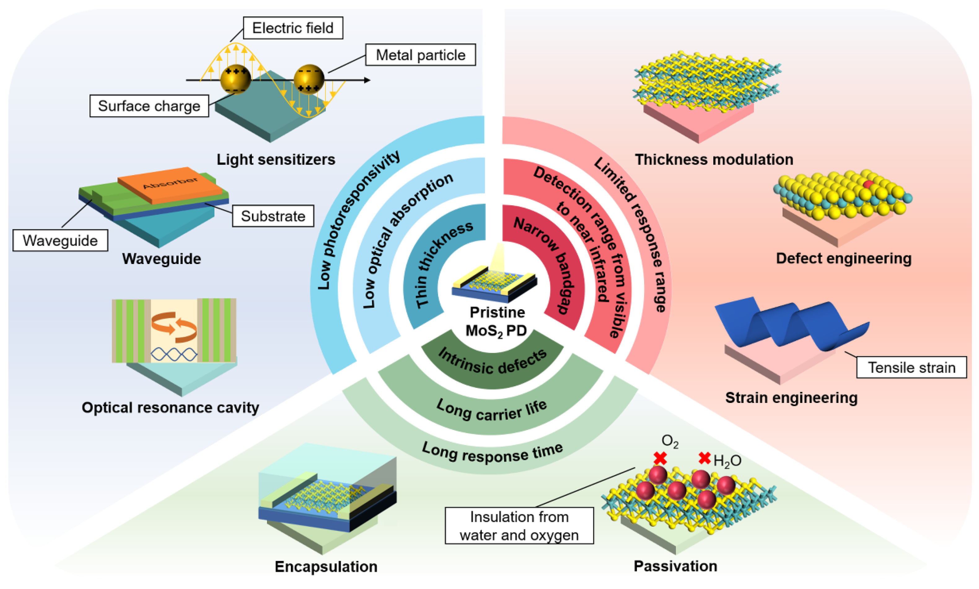
Figure 3.
Schematic of three typical optical resonance cavities. (a) Fabry-Perot type cavity. (b) 2D photonic crystal cavity. (c) Whispering gallery mode microcavity. Reproduced with permission from ref [92]. Copyright 2020 John Wiley & Sons, Inc.
Figure 3.
Schematic of three typical optical resonance cavities. (a) Fabry-Perot type cavity. (b) 2D photonic crystal cavity. (c) Whispering gallery mode microcavity. Reproduced with permission from ref [92]. Copyright 2020 John Wiley & Sons, Inc.

Figure 4.
(a) Photoresponse of defective-MoS2 PDs under vacuum or exposed to air. (b) Gas response of defective-MoS2 PD with and without MA3Bi2Br9 treatment. (c) Corresponding schematic illustration of defect states in the electronic band of MoS2. Reproduced with permission from ref [103]. Copyright 2018 American Chemical Society.
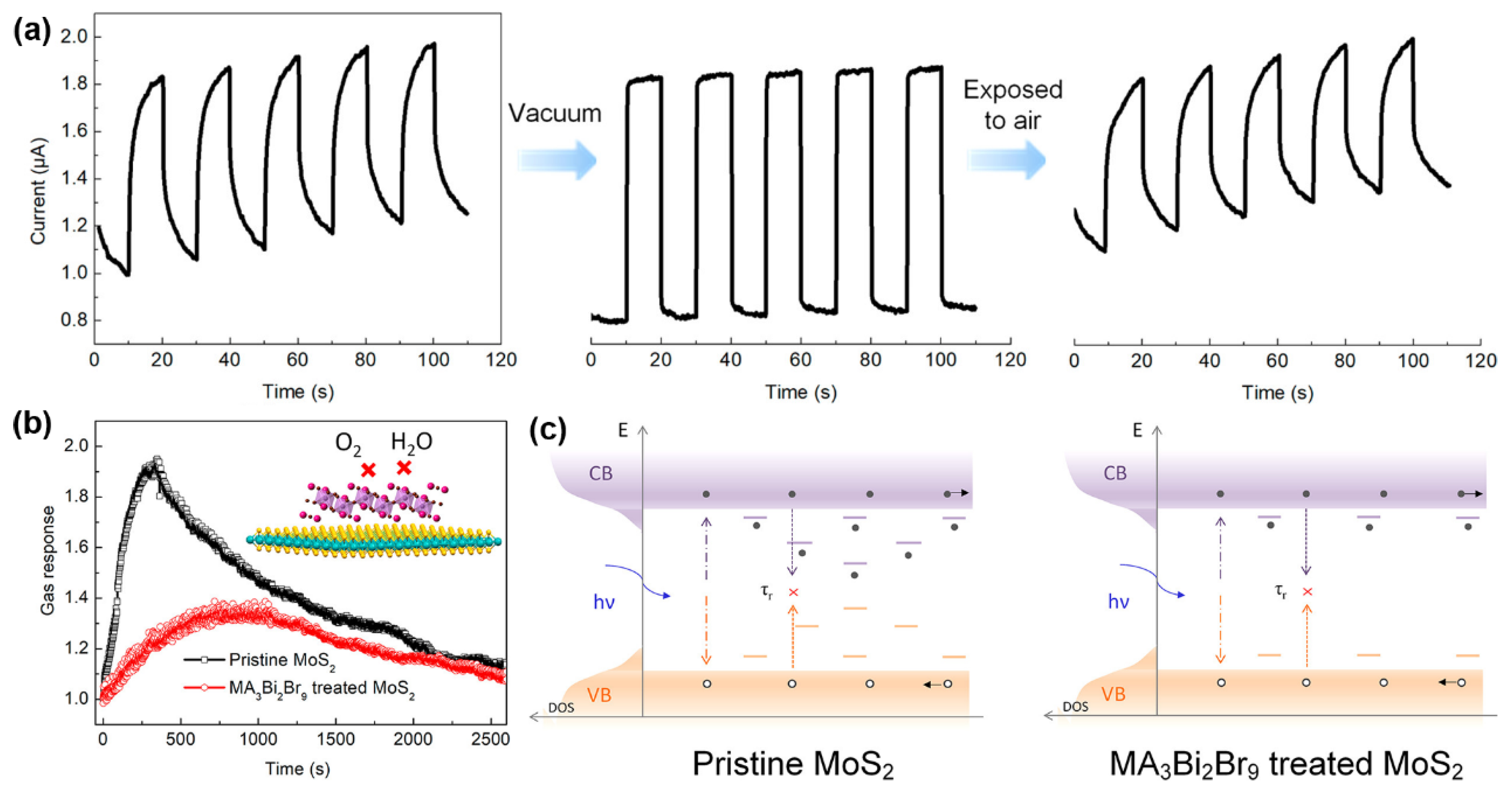
Figure 5.
Band structures of bulk MoS2 (a), quadrilayer MoS2 (b), bilayer MoS2 (c), and monolayer MoS2 (d). Reproduced with permission from ref [116]. Copyright 2010 American Chemical Society.
Figure 5.
Band structures of bulk MoS2 (a), quadrilayer MoS2 (b), bilayer MoS2 (c), and monolayer MoS2 (d). Reproduced with permission from ref [116]. Copyright 2010 American Chemical Society.
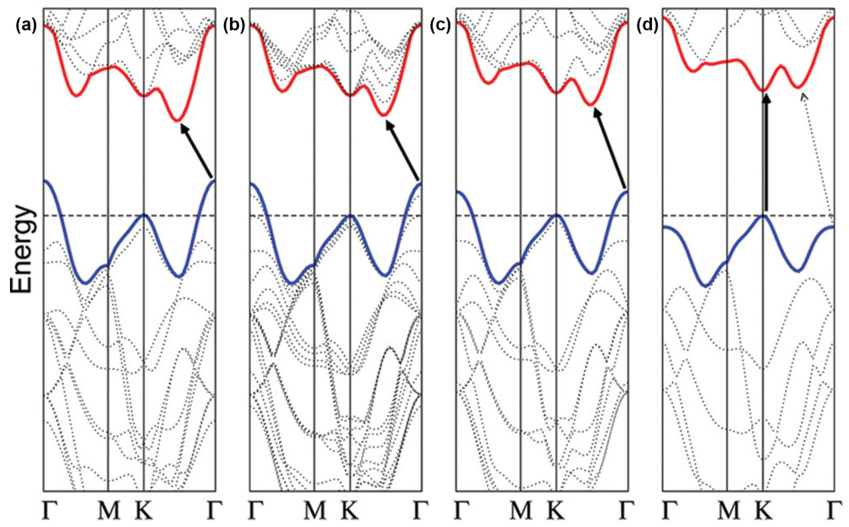
Figure 6.
(a) Schematic presentation of the synthesis processes of wrinkly MoS2 flakes. (b) Optical microscopy image and (c) atomic force microscopy image of a wrinkled MoS2 flake (d) Photoluminescence spectra of wrinkly MoS2 flakes at the different locations (flat and wrinkle parts). (e) Relationship between the direct bandgap transition and the localized tensile strain. Reproduced with permission from ref [114]. Copyright 2013 American Chemical Society.
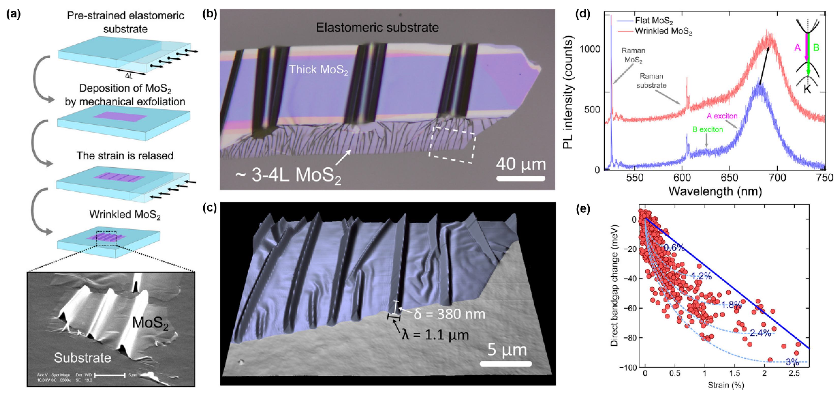
Figure 7.
(a) The relationship between S/Mo ratio (x) and bandgaps of 2D MoSx. (b) Interface energy band diagram between Au electrodes and 2D MoSx before (b) and after (c) applying THz radiation. Electron-transport behavior in PDs based on 2D MoSx with (d) and without (e) applying THz radiation. (f) The relationship between photocurrent or R and bias voltage. Reproduced with permission from ref [141]. Copyright 2020 American Chemical Society.
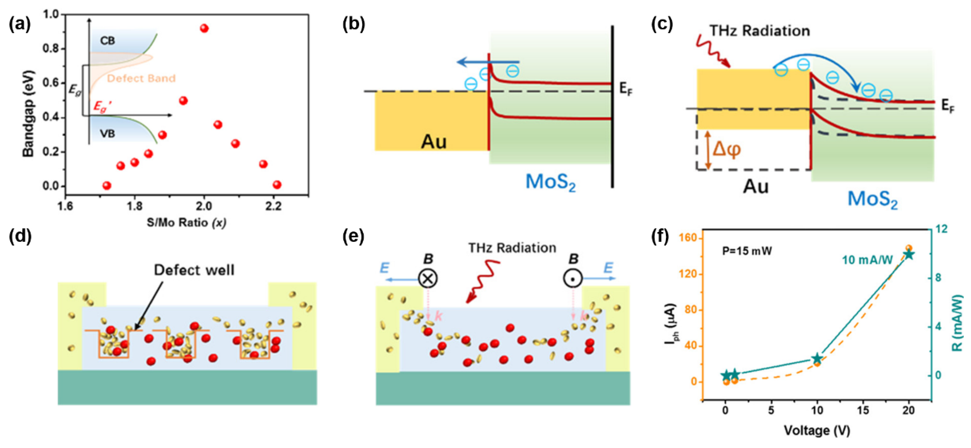
Figure 8.
(a) A diagram showing the setup utilized in a MoS2 PD. (b) Relationship between strain and temperature of polycarbonate. (c) Differential reflectance spectra measured at different temperatures. Reproduced with permission from ref [149]. Copyright 2019 Elsevier.
Figure 8.
(a) A diagram showing the setup utilized in a MoS2 PD. (b) Relationship between strain and temperature of polycarbonate. (c) Differential reflectance spectra measured at different temperatures. Reproduced with permission from ref [149]. Copyright 2019 Elsevier.
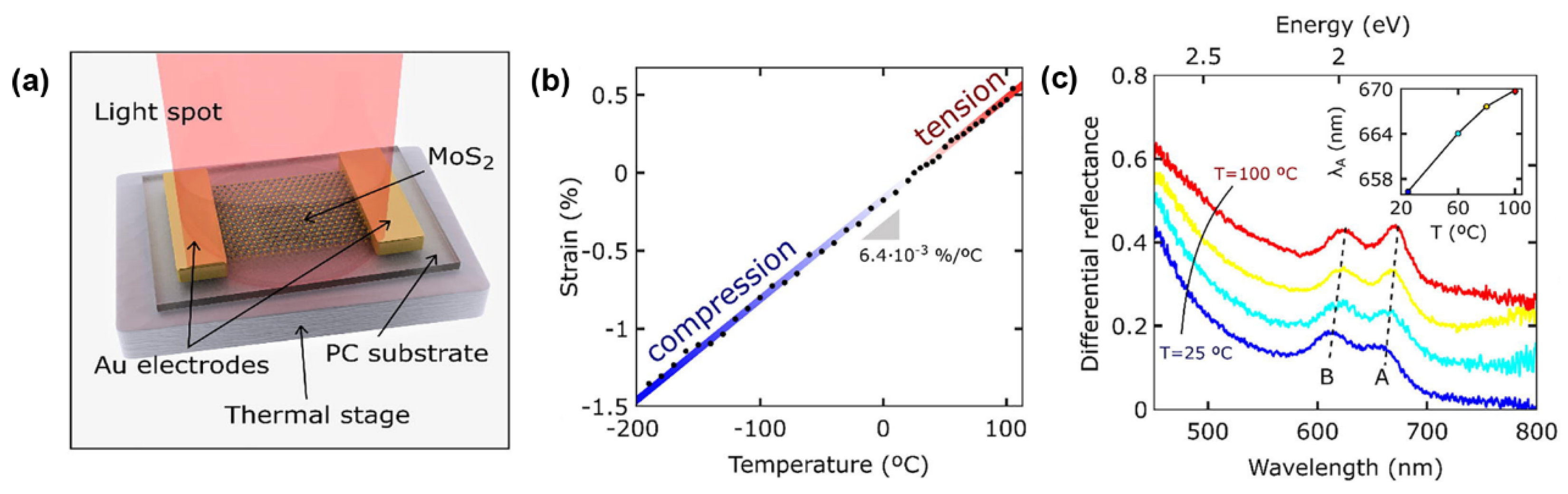
Figure 9.
Graphical illustration of mixed-dimensional heterostructures with different combination formats including (a) 0D/2D, (b) 1D/2D, and (c) 2D/3D mix-dimensional structures.
Figure 9.
Graphical illustration of mixed-dimensional heterostructures with different combination formats including (a) 0D/2D, (b) 1D/2D, and (c) 2D/3D mix-dimensional structures.

Figure 10.
(a) Schematic presentation of LSPR in Au-NP grating. (b) Extinction spectra of different Au NPs and (c) transfer characteristic of the Au-NP/MoS2 PD. Reproduced with permission from ref [170]. Copyright 2020 American Chemical Society. (d) Schematic diagrams of Au-MoS2-Au PDs. (e) Light intensity-dependent R of Au-MoS2 and Au-MoS2-Au PDs. (f) Schematic presentation of interface energy band of Au-MoS2-Au. (g) Calculated electrical field strength distributions of Au NPs on the two surfaces of MoS2. (h) Photocurrents of Au-MoS2-Au PDs under different light intensities. (i) Possible charge-transfer processes of Au-MoS2-Au PDs under visible light. Reproduced with permission from ref [171]. Copyright 2022 American Chemical Society.

Figure 11.
(a) Schematic representation of MoS2 PD (MNPs refer to the MXene QDs with an average size of 8 nm). (b) I-V plots of pristine MoS2 and MXene-QD/MoS2 PD in dark. 2D photoresponse maps of (c) MXene-QD/MoS2 PDs and (d) pristine MoS2 under 635 nm excitation wavelengths. Reproduced with permission from ref [176]. Copyright 2022 American Chemical Society.
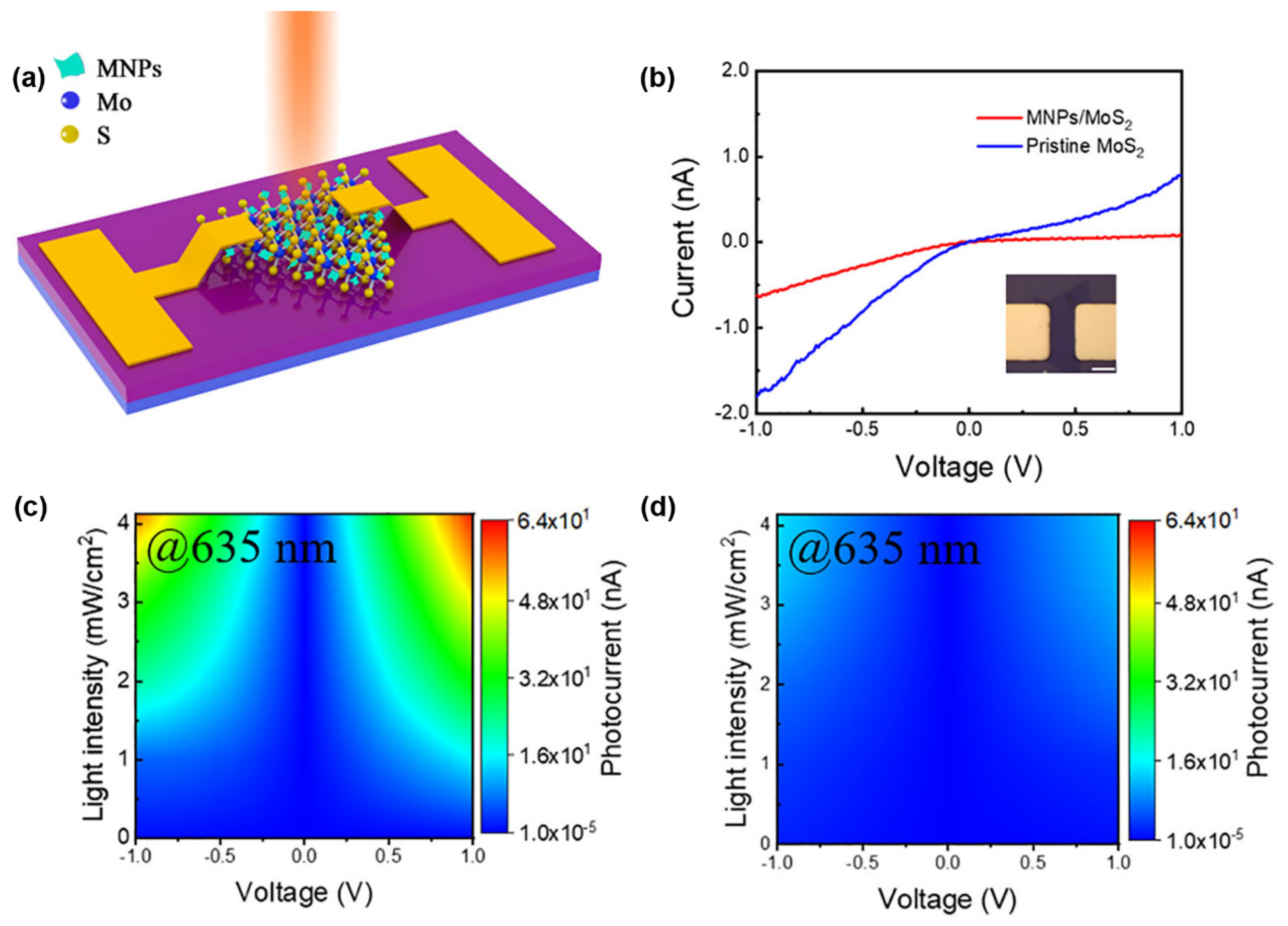
Figure 12.
(a) 3D schematic representation of SnS2-QDs/MoS2 PD. (b) Schematic illustration of band structures of SnS2 QDs and monolayer MoS2. (c) R of SnS2-QDs/MoS2 PD. Reproduced with permission from ref [174]. Copyright 2022 American Chemical Society.
Figure 12.
(a) 3D schematic representation of SnS2-QDs/MoS2 PD. (b) Schematic illustration of band structures of SnS2 QDs and monolayer MoS2. (c) R of SnS2-QDs/MoS2 PD. Reproduced with permission from ref [174]. Copyright 2022 American Chemical Society.
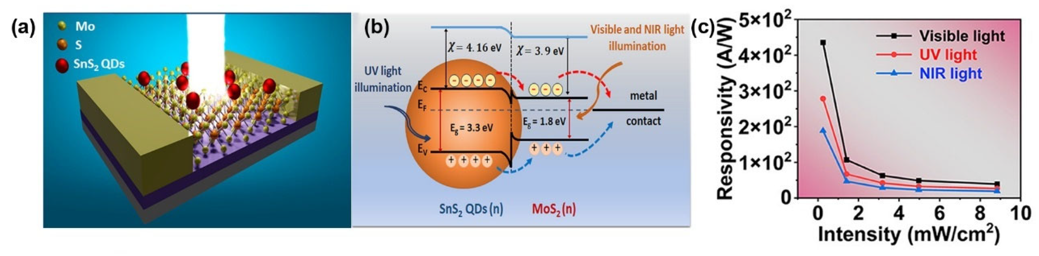
Figure 13.
Device structure and interfacial charge-carrier transport behavior for the n-ZnO/p-MoS2 PDs with a forward biasing voltage (a), with a forward biasing voltage and under UV light (b), and with a forward biasing voltage and under green light (c). Reproduced with permission from ref [182]. Copyright 2020 John Wiley & Sons, Inc.
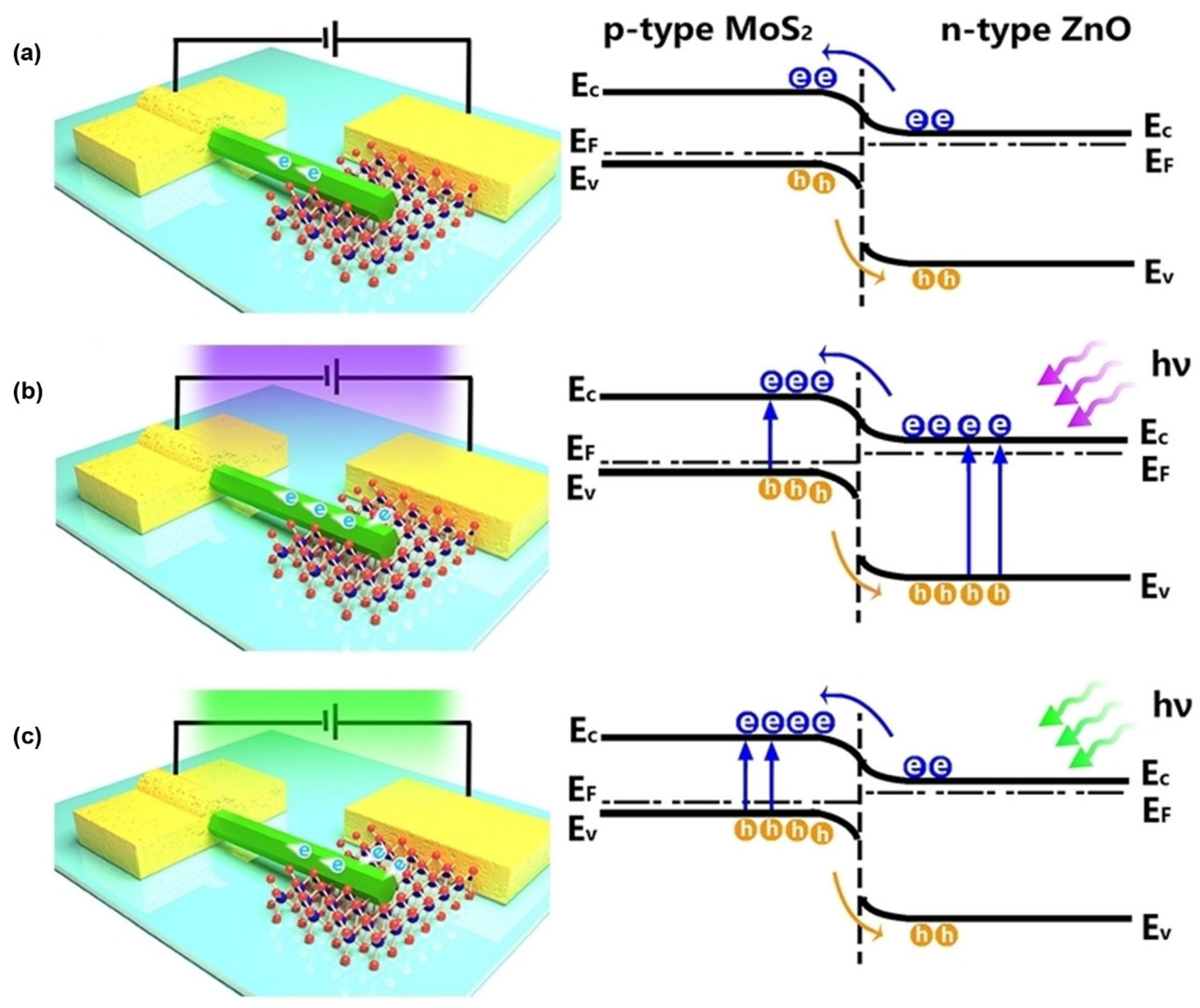
Figure 15.
(a) Schematic presentation of the device structure of a MoS2/CsPbBr3 PD. Charge production and transport processes at the MoS2/CsPbBr3 heterojunction in the dark (b) and under light illumination (c). (d) UV-vis absorption spectra of MoS2, CsPbBr3, and MoS2/CsPbBr3 heterojunction. (e) I-V characteristics plots of MoS2, CsPbBr3, and MoS2/CsPbBr3 heterojunction with and without laser illumination. (f) Relationship between R vs. power intensity. Reproduced with permission from ref [191]. Copyright 2018 American Chemical Society.
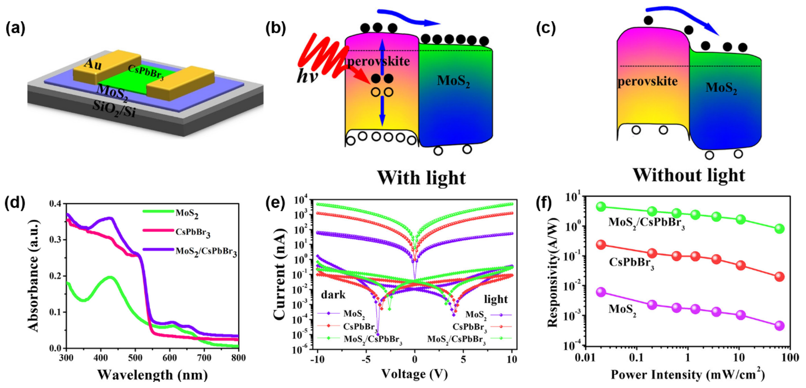
Figure 16.
(a) Schematic presentation of device structure of graphene/2D MoS2 PD under illumination. (b) A diagram of photocurrent generation of graphene/2D MoS2 PD. (c) Current-voltage of graphene/2D MoS2 PD in the dark and under 100 mW/cm2 illumination. (d) R of graphene/2D MoS2 PD at different wavelengths. (e) Photoconductivity of graphene. Reproduced with permission from ref [194]. Copyright 2015 American Chemical Society.
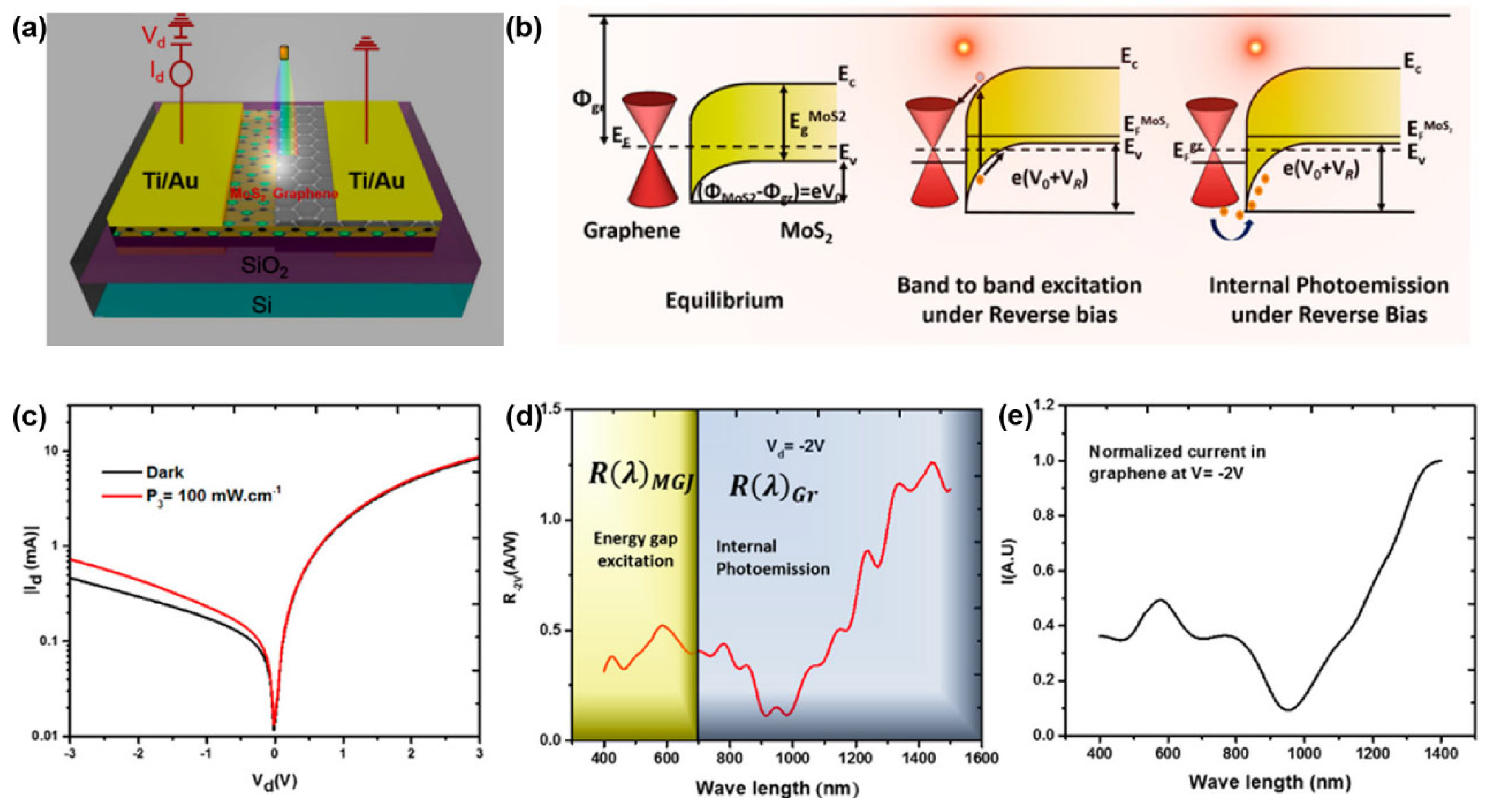
Figure 17.
(a) Schematic picture of a CZTS/MoS2 PD. (b) Charge transfer mechanism at CZTS/MoS2 heterojunctions. (c) Estimated R of the CZTS/MoS2 heterojunction PD for various wavelengths at a bias of 6 V. Reproduced with permission from ref [215]. Copyright 2020 Elsevier.
Figure 17.
(a) Schematic picture of a CZTS/MoS2 PD. (b) Charge transfer mechanism at CZTS/MoS2 heterojunctions. (c) Estimated R of the CZTS/MoS2 heterojunction PD for various wavelengths at a bias of 6 V. Reproduced with permission from ref [215]. Copyright 2020 Elsevier.
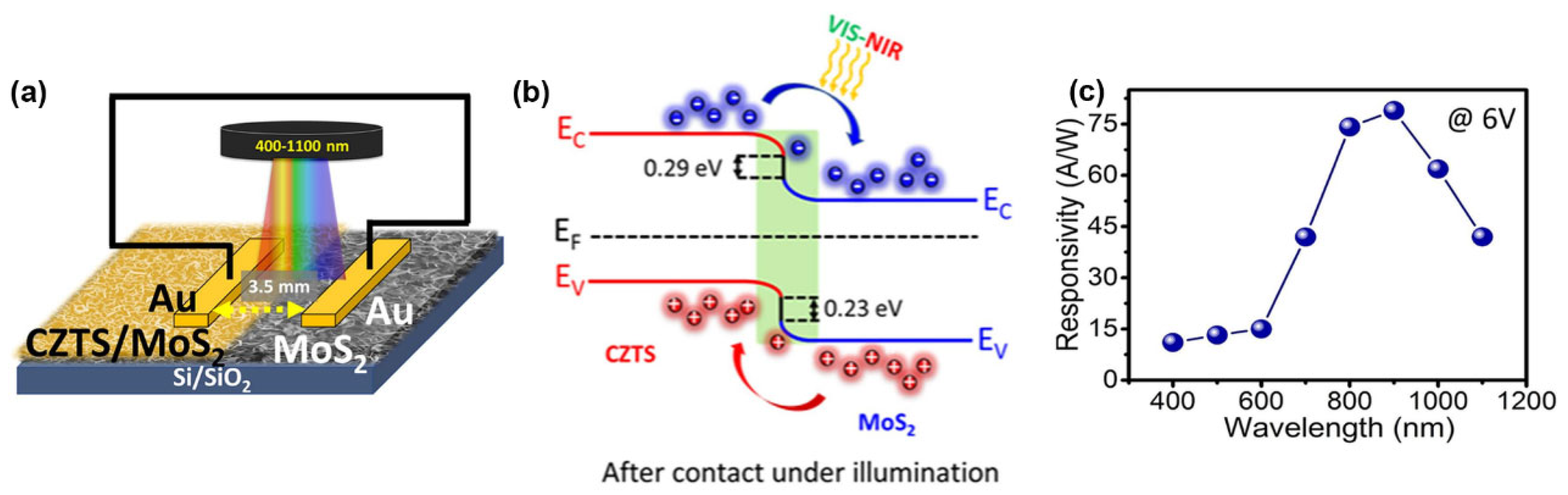
Figure 18.
(a) Schematic presentation of 3D structures of MoS2/MoSe2/GaN heterostructures. (b) Schematics of the energy band diagram for the heterostructures. (c) Photoswitching of D1, D2, D3, and D4 devices (D1, GaN/MoSe2; D2, GaN/MoS2; D3, GaN/MoS2/MoSe2; D4, GaN/MoSe2/MoS2). (d) UV (λ = 365 nm) intensity-dependent R for different device configurations. (e) Specific detectivity for different device configurations. Reproduced with permission from ref [220]. Copyright 2023 American Chemical Society.
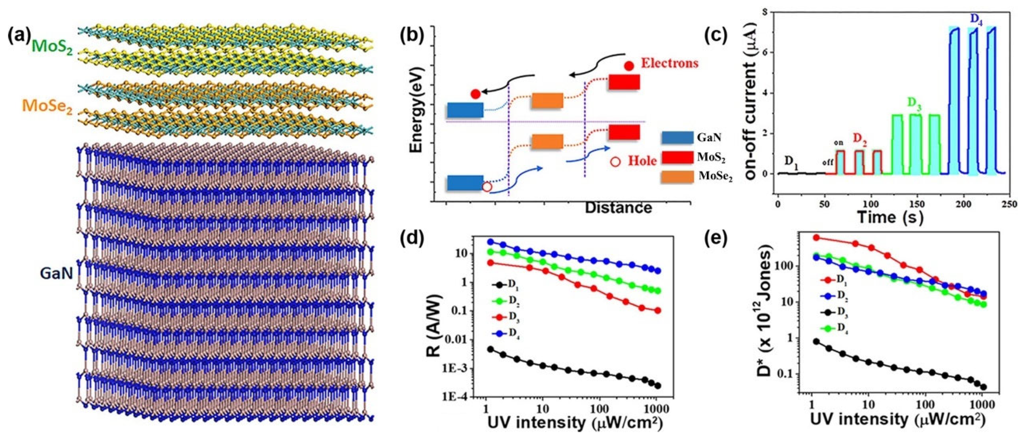
Table 3.
Summary of various photoconductive-type PDs based on MoS2-based nanocomposites for detecting pollutants.
Table 3.
Summary of various photoconductive-type PDs based on MoS2-based nanocomposites for detecting pollutants.
| Sensing Material | Main synthesis method | Target | R (A·W-1) | Linear range | Detection limit | Wavelength | Ref. |
| Few-layer MoS2/Si | CVD | Rhodamine 6G | 0.1413 | 10-3 -10-9 M | 10-9 M | White light | [154] |
| rGO/MoS2 | Hydrothermal | Escherichia Coli O157:H7 | - | 5.0-5.0 × 10⁶ CFU·mL-1 | 2.0 CFU·mL–1 | NIR | [155] |
| Pd/MoS2@g-C3N4 | Solvothermal exfoliation | Cu2+ | 9.3 | 1 μM-1 mM | 0.21 μM | - | [156] |
| Au@Ag-MoS2/ct-DNA/CdSe | ME | Hg2+ | - | 10 pmol·L−1 -100 nmol·L−1 | 5 pmol·L−1 | 430 nm | [157] |
| rGO/MoS2 | Hydrothermal | Aflatoxin B1 | - | 0.001-100 ng·mL-1 | 2.18 pg·mL-1 | 465 nm | [158] |
| MoS2 QDs/TiO2 NTs | Hydrothermal | Atrazine | - | 0.5-107.8 ng·L-1 | 0.2 ng·L-1 | Vis-UV | [159] |
| MOF-MoS2 | Hydrothermal | Hg2+ | - | 0.01-1000 nM | 0.25 pM | - | [160] |
| ZnO/MoS2 | Hydrothermal | Cr (VI) | - | 0.008-640 µM | 7 nM | - | [161] |
| ZnIn2S4/V-MoS2 | Hydrothermal | Aflatoxin B1 | - | 0.05-50 ng·mL-1 | 17 pg·mL-1 | Vis-UV | [162] |
ME: mechanically exfoliated; CVD: chemical vapor deposition; rGO: reduced graphene oxide; QDs: quantum dots; NTs: nanotubes; MOF: metal-organic framework; UV: ultraviolet; Vis: visible; V-MoS2: S-vacancy engineered MoS2; - The data are not available.
Disclaimer/Publisher’s Note: The statements, opinions and data contained in all publications are solely those of the individual author(s) and contributor(s) and not of MDPI and/or the editor(s). MDPI and/or the editor(s) disclaim responsibility for any injury to people or property resulting from any ideas, methods, instructions or products referred to in the content. |
© 2024 by the authors. Licensee MDPI, Basel, Switzerland. This article is an open access article distributed under the terms and conditions of the Creative Commons Attribution (CC BY) license (http://creativecommons.org/licenses/by/4.0/).
Copyright: This open access article is published under a Creative Commons CC BY 4.0 license, which permit the free download, distribution, and reuse, provided that the author and preprint are cited in any reuse.


