
Submitted:
17 January 2025
Posted:
20 January 2025
You are already at the latest version
Abstract
Printing techniques have been instrumental in developing flexible and stretchable electronics including organic light-emitting diode displays, organic thin film transistor arrays, electronic skins, organic electrochemical transistors for biosensors and neuromorphic computing, as well as flexible solar cells with low-cost processes such as inkjet printing, ultrasonic nozzle, roll-to-roll coating. The rise of additive manufacturing provides even more opportunities to print electronics in automated and customizable ways. In this work, we will review the current technologies of printing electronics (including printed batteries, supercapacitors, fuel cells, sensors), especially with 3D printing. In this age of ongoing AI revolution, the application of AI algorithms is discussed, in terms of combining them with 3D printing and printing electronics for a smart and efficient future.
Keywords:
Additive Manufacturing
; Batteries
; Fuel Cells
; Electronics
; Machine Learning
; AI
1. Introduction
Electronics Printing is an emerging technique that has been used in fabricating flexible and thin film displays, transistor arrays, solar cells, biosensors such as electronic skins, neuromorphic computing, and batteries, which traditionally involves low-temperature, low-cost processes including tape casting, inkjet printing, roll-to-roll manufacturing, or spray with ultrasonic nozzle.1,2 The current trend of 3D printing provides additional opportunities in printing electronics, for personalization, prototyping, cost control, and reduced reliance on supply chains and toolings.3,4
For example, the designer freedom and manufacturing cost of conventional battery manufacturing processes can be significantly enhanced by printing.2 In conventional battery manufacturing, a typical streamline consists of (1). slurry preparation, (2). tape casting and drying, (3). calendaring, (4). electrode cutting, (5). packaging, and (6). electrolyte filling, while in 2D or 3D battery printing, the number of steps are narrowed down to: (1) electrode/ electrolyte pattern design, (2). filament or ink preparation, (3). printing (including pre- and/or post- printing treatments), (4) packaging.2
Furthermore, the automation offered by electronics printing may be coupled with “digital twins” building, machine-learning-algorithm-based process optimization, and AI-driven discoveries, to prepare us for the upcoming societal challenges on healthcare, global warming, energy production, and more.5
In this review, we will first discuss printing electronics in general (e.g., contact and non-contact printing, electrostatic printing), then highlight recent progress in 3D printing electronics (including printing supercapacitors, sensors, batteries, and fuel cells). We will end with the current status of AI applications in 3D and electronics printing, summarizing popular algorithms and examples of optimization processes. Also it is important to classify that there are other electronic printing/patterning methods based on lithographic and non-lithographic patterning. We will mainly be concerned with non-lithographic printing and patterning, meaning a direct ink or material is transferred, rather than those involving etching or even photolithography.
2. Printing Electronics
While silicon-based traditional electronics provide unmatched processing speeds for our computers and heavily rely on clean-room facilities such as lithography, printed electronics involve almost all components of conventional electronics, while providing opportunities for low-cost personalization, multifunctionality, flexibility, and better interface with biological and complicated surfaces.1 Figure 1 are plots showing the publication numbers in the Web of Science database related to printable electronics. A steady rising trend is clear in Figure 1a over the years. Inks using 2D materials, metal, and oxide nanoparticles are compared in Figure 1b, demonstrating the popularity of these inks.6
Contact printing, with the relative positioning of the printing area and non-printing area, can be divided into planographic (screen printing, offset printing), relief (letterpress, flexography), and intaglio (gravure printing).8 For example, in screen printing, the printing areas are flat with non-printing areas, but pre-patterned with a mesh screen permeable to ink; in gravure printing, the printing areas are engraved below the flat surface of the non-printing areas; and in flexography, a flexible relief plate is adopted, with the non-printing areas below the printing areas.8
Non-contact printing techniques (Figure 2) include inkjet, aerosol, filamentary printing, or electrostatic printing, sometimes with UV-light curing.6 A typical nozzle size for Inkjet printing is 20 microns, an order of magnitude smaller than that of aerosol-jet printing (100-300 microns). In contrast, the nozzle sizes for electrostatic printing may range from 0.2 to 100 micron.6 Inkjet printing ejects non-viscous droplets that collapse or evaporate on substrates, electrostatic printing drives with surface-tension-limited meniscus formation under an applied electrical field, and aerosol printing relies on a carrier gas to bring atomized ink from ink reservoir to print head, a sheath gas to drive the aerosol to substrates, and the focusing ratio between sheath and carrier gas flow rate to control printing resolution (Figure 2a-b,d).6 Extrusion printing (Figure 2c) can be used for 2D and 3D object manufacturing, which will be detailed in the next section.
Electrostatic printing and electrospinning have been an important area for next-generation energy and medicine applications.9–14 Both electrostatic printing and electrospinning are techniques of utilizing electric fields to manipulate formulated precursors, thus extruding materials. Although electrospinning generates nano- to submicron- scale fibers in a membrane form with high intrinsic porosity and surface area, electrostatic printing allows the deposition of materials in a precise and controlled manner.13,14 The shared apparatus in these two techniques is the charged nozzle and collector bearing the opposite charge. The charged nozzle facilitates the charges of chemical components in the formulation, facilitating the transformation from droplets to jets (Taylor cone) and directing the trajectory of formulated materials to the target, and adhesion to the substrates.13–15 In electrospinning, the electric field changes lead to various fiber morphologies as tunable parameters in membrane structure and function.15 In electrostatic printing, in addition to the above factor, it plays critical roles in printing resolution due to its impact on droplet size and the direct writing nature of this technique.13 Moreover, with early fundamental investigation of electrospinning in 1900s and development in modern electrospinning techniques16, commercial bench scale, pilot scale and manufacturing electrospinning apparatus with controlled environment are available for both R&D work and production. In contrast, electrostatic printer is still in its infancy, offering advantages in electronics fabrication with more precision and controlled pattern compared to electrospinning.13
Wang et al. reviewed recent progress of electrospun nanofiber based soft electronics and these fibrous membranes exhibit broad applications in sensors, photo detectors, energy storage, and transistors with known primary advantages of large surface area and flexibility. It also pointed out the limitations in fiber formation among common chemicals required for electronics, and the challenges when blends and composites are used.14 Some examples of possible applications of the resultant nanofiber assemblies in energy storage include: (1) Tubular carbon network for enhanced battery electrodes via electrospun polymer templates, (2) fillers to enhance ion conductivity of solid electrolytes, (3) porous,flexible membranes for high-performance separators and stand-alone electrodes, and (4) 3D host for lithium metal and sulfur.9
3. 3. D Printing of Electronics
Additive manufacturing (AM) can build objects one layer at a time, using techniques such as jetting, lamination, extrusion, powder fusion, deposition, and photopolymerization.4,17–20 Compared to traditional subtractive manufacturing, AM is much less reliant on supply chains and tooling, while excels in complicated geometries and customization.
The various electronics that can be manufactured via additive manufacturing include transistors, diodes, multilayer circuits, solar cells, interconnects, antennas, batteries, supercapacitors, fuel cells, and sensors.3,21–26
Flexible, safe, light, stable supercapacitors with excellent power density and cyclability can be achieved via contact or non-contact printing of customer-designed current collectors, substrates, electrodes, as well as electrolyte materials.27 Choi et al. demonstrated a solid-state, paper-based, flexible supercapacitor, by printing carbon nanotubes, ionic liquid, and photo-crosslinkable triacrylate polymer electrolyte, along with a cellulose nanofibril-based primer layer and Ag-nanowires-based electrodes.28 Mevada et al. enhanced activated carbon with catechin hydrate grafting and printed choline chloride /urea deep eutectic system (DES)-based electrolytes, to a capacitance of 75 F/g, potential window of 2.0 V, 90% cycling stability after 10k cycles (Figure 3).29 To tackle high capacitance, large mass loading, structural complexity, and a high degree of system integration, 3D-printing techniques need continued adaptations to achieve highly porous structures in interdigital, modular, or integrated circuit designs for their potential in various supercapacitor usage scenarios.30
Compared to silicon or inorganic semiconductor-based rigid sensors widely used in current robotics and communication systems (such as cell phones), flexible sensors are necessary in future healthcare and internet-of-things scenarios.31 Wang et al., reviewed processes and applications of low-cost inkjet-printable sensors, which can be light, flexible, and fabricated with mass production.32 Ponan and Harnsoongnoen demonstrated that 3D printing with conductive polymer filaments can make an interdigital sensor for salt and sucrose on an insulating substrate (Figure 4).33 The sensing was based on electrical responses using a direct current.
Battery printing can enable safe, environmentally-friendly, flexible forms of energy storage.35–40 Additive manufacturing of batteries is suitable for miniaturized electronics, implantable devices, remote sensors, transmitters, smart cards, and the Internet of Things (IoT) networks, with design freedom, higher (area or volume) energy densities, larger power density, and reduced cost, via techniques such as direct ink writing (DIW), fused deposition modeling (FDM), inkjet printing (IJP), and stereolithography (SLA).2 For example, Martinez et al.,41 developed a multiprocess to 3D print sodium-ion batteries, in which DIW is used for positive electrodes and vat photopolymerization (VPP) is used for gel polymer electrolytes. With a Na0.44MnO2 electrodes, 3D printed electrolytes show room-temperature ionic conductivities up to 3.3 × 10⁻³ S·cm−1, and a stability window of 4.8 V.41 Ma et al., used DIW-based Printing to fabricate planar, flexible sodium-ion microbatteries, with microelectrodes up to 1200 µm thickness, 4.5 mAh cm−2 areal capacity, 3.6 mAh cm−2 rate capability, for as long as 6000 cycles.42
Furthermore, 3D -printing-enabled fuel cell technologies are gaining traction. As a clean energy carrier, hydrogen is undergoing an unparalleled surge in interest, with numerous countries launching national hydrogen strategies that are accelerating the emergence of a global hydrogen economy,43 targeting applications ranging from ammonia production, steel refining, to synthetic fuels from captured CO2 or electricity through a fuel cell.44–46 Fuel cells are being extensively developed for heavy-duty transportation, such as Class 8 trucks, trains, ferries, and airplanes.47 3D printing, or additive manufacturing, has emerged as a transformative technology in the development and production of fuel cells.48,49 This approach enables the creation of complex and customized components that enhance the performance, efficiency, and cost-effectiveness of fuel cell systems: (1) One of the primary advantages of 3D printing in fuel cell applications is the ability to produce intricate parts, such as proton exchange membranes (PEM), flow field plates, and gas diffusion layers, with high precision. Traditional manufacturing methods often struggle with the complexity of fuel cell components, but 3D printing can generate complex geometries that optimize the flow of reactant gases and improve overall fuel cell efficiency. (2) 3D-printed flow field plates are a key area of interest, as they can be designed with optimized channel structures to ensure even distribution of reactants, reducing energy losses and enhancing the fuel cell’s performance. (3) Furthermore, 3D printing enables the design of lightweight and compact parts, essential for fuel cell applications in sectors like automotive and aerospace, where space and weight constraints are critical. (4) The rapid prototyping capabilities of 3D printing also accelerate the development process, allowing for faster iteration and testing of new designs, significantly shortening the development cycle. (5) Additionally, the ability to use various materials in 3D printing, such as metals, ceramics, and polymers, offers the potential for producing highly durable and corrosion-resistant fuel cell components. This versatility also aids in optimizing the performance and lifespan of fuel cells under varying operating conditions. Despite the numerous benefits, challenges such as (1) material limitations related to the printing process, (2) scalability, and (3) the need for post-processing 3D-printed parts remain. Nevertheless, ongoing advancements in 3D printing techniques and materials are expected to overcome these barriers, making it a promising tool for the future of fuel cell technology. For example, Lira et al. reported a solid oxide cell (SOC) benefited from advanced ceramic 3D printing methods such as stereolithography (SLA) and robocasting,50 which allow for the creation of complex shapes, improved interfaces, and reduced material waste. This study focuses on large-area SOCs (25 cm²) fabricated using SLA 3D printing, with electrolyte supports made of yttria-stabilized zirconia (8YSZ) and composite electrodes of nickel (fuel electrode) and lanthanum strontium manganite (oxygen electrode). The printed electrolytes featured advanced honeycomb geometries for enhanced performance. In fuel cell mode, the cells generated up to 3.5W with a peak power density of 240-220mW/cm² at 950°C, and in the electrolysis mode, they provided 7.3W with a current density of 340mA/cm² at 1.3V. A long-term degradation test at 900°C over 1150 hours showed minimal degradation of 11mV/kWh. In comparison, solid oxide fuel cells have also been manufactured using traditional contact and non-contact printing methods. For example, Han et al., developed an inkjet-printed submicron-thickness ceramic electrolyte that maintained a stable microstructure during electrochemical testing.51 Somalu et al., reviewed the application of screen printing in fabricating solid oxide fuel cell electrodes and electrolytes with thickness between 10 and 100 µm.52 The oxide particles, binder, dispersant, or solvent in the screen printing ink recipes contribute to their overall rheology, as well as mechanical, electrical, and electrochemical performances.
4. AI in 3D and Electronics Printing
Machine learning can be effectively combined with printing and additive manufacturing to enhance efficiency at another level,5,53–59 in areas ranging from planning, design automation, property prediction, process monitoring and optimization, to quality control, maintenance scheduling, and defect detection.60–65 In situ or customized additive manufacturing, with bio-electroactive inks and open-source AI algorithms, can lead to wearable and smart biosensors at a fraction of the current cost for a better healthcare future via efficient diagnostics and regenerative medicines.
Figure 5 analyzes the application areas of AI models that enhance 3D printing. For fused diffusion modeling (FDM), nozzle temperature, flow rate, and pressure can be significant, while parameters such as laser power and scan speed are critical for Powder Bed Fusion (PBF). These explain why 42% of the AI optimizations in Figure 5 deal with the manufacturing process. Other essential subjects of AI algorithms include: (1) quality predictions of the printed products (for example, roughness, mechanical strength), (2) simulation optimization for reduced computational costs, (3) design, and (4) topology optimization.
Artificial neural network (ANN) was used to simulate melting kinematics and filament flows in FDM processes.67 Mohamed et al., used FDM settings as inputs (features) to predict the resultant cylinder dimensions.67 The ANN model in Figure 6 showcases the internal construct of the algorithm.The algorithm uses features such as slice thickness, raster-to-raster air gap, deposition angle, printing direction, bead width, and shell number, to predict the length and diameter changes of the 3D-printed cylinders.
Some of the popular algorithms used for AI-aided Manufacturing include support vector machine (SVM), Bayesian networks, and deep learning ( including computer vision and natural language processing).68 Figure 7 has a pie chart of AI algorithms for above-mentioned (Figure 5) publications on 3D printing optimizations.66 In this chart, deep learning (DL) models are specified separately, and other regression and classification models are under the general machine learning (ML) group. DL models in the chart include artificial neural network (ANN), convolutional neural network (CNN), Generative Adversarial Artificial Networks (GAAN), and Long Short-Term Memory (LSTM) networks.66 GAAN relies on a generator and discriminator to achieve high-performance unsupervised learning, while neural networks are designed for supervised learning.68 Recurrent neural networks, such as LSTM and Attention models, provide the capability to selectively discard or keep information from previous frames.68
In the field of AI-automated 3D printing, Gongora et al.,69 developed a Bayesian experimental autonomous researcher (BEAR) for additive manufacturing, to combine high-throughput automated experimentation (Figure 8) and Bayesian optimization (Figure 9). This achieved a 60-fold experimental iteration reduction to maximize the toughness of the printed structure, as compared to a grid search. It is noted that this was achieved with limited experimental data availability. An automated polymer analysis and discovery array (PANDA) combined high-throughput fluid handling, electrodeposition, electrochemistry, and optical measurements in 96-well plates to maximize electrochromic switching of conductive polymer with Bayesian-optimization generated monomer concentration, deposition time and voltage.70 We expect that the future adaptation of similar approaches will benefit electronics printing and optimization.
(A) Experimental system composed of (i) five dual extruder fused deposition modeling (FDM) printers (M3, MakerGear), (ii) a six-axis robotic arm (UR5e, Universal Robotics), (iii) a scale (CP225D, Sartorius), and (iv) a universal testing machine (5965, Instron Inc.). (Photo credit: Aldair E. Gongora and Bowen Xu, Boston University). (B) Model “crossed barrel” family of parametric structures with two circular platforms that are held apart by a series of n hollow columns of outer radius r and thickness t and that are twisted with an angle θ. Force F and corresponding displacement D from the testing of (C) a crossed barrel that did not yield before ~5 kN (designated too strong), (D) a crossed barrel that failed in a brittle manner (designated “brittle”), and (E) a crossed barrel that exhibited appreciable strength after an initial yield point (designated “ductile”). (Figure and Caption from reference69 without change, under Creative Commons Attribution 4.0 International License.7)
It is important to point out, for both additive and subtractive manufacturing techniques, materials property and processing need to be optimized, and this can be automated by machine learning. For example, the development of new sensors will require optimized materials properties together with high-efficiency, low-cost manufacturing, often with hybrid materials. Multi-material and 3D/4D printing technologies will rely more on AI/ML (artificial intelligence / machine learning) methods,71 to revolutionize materials and composition design for tailored properties, dynamic responsiveness, processability (viscosity, curing behavior, thermo-mechanical, etc. ), and rapid prototyping-to-production transition. With digital twins and workflows for materials selection, sensor design, and optimized printing, one can significantly reduce time and costs for future electronics and 3D printing development.72 For instance, composites with up to 91% filler were formulated with an elastomer matrix for 3D printing, using image-driven ML model and finite element analysis (FEA).73 Interfacial properties in 3D printed particle-matrix composite can be modeled with ML, FEA, and empirical experiments for composite sensor design.74 ML and structure-composition-processing property (SCPP) relationship are combined to 3D print polyvinylidene fluoride (PVDF)/ molybdenum disulfide (MoS2) composites with boosted piezoelectric sensing behavior, providing a promising route to the design and fabrication of high-performance flexible electronics and wearable device via AI-aided 3D printing.71,75
In addition, templated or guided assembly is widely used to fabricate functional nanomaterials,76–78 organic electronics,79 and ionics 80,81. These methods offer unique self-assembly-induced properties in a vast processing parameter space (including varied molecular structures of the crystallization mediator, assembly conditions), and can be combined with 3D printing to more efficiently optimize the resultant nanostructures and electrical performances.
5. Conclusion
Printing electronics and AI are a natural combination of our progress in the Internet of Things, Industrial Revolution 4.0, and smart manufacturing. The continued interactions between the two will spark inspiration for a personalized, environment-friendly, energy-efficient future for Mankind. This review summarizes recent advances in electronics printing (especially with additive manufacuring), and AI-aided electronics printing, laying a foundation to inspire future developments in machine learning and algorithm-driven manufacturing of flexible electronics, supercapacitors, batteries, sensors, and fuel cells with reduced cost and higher performance.
Acknowledgments
This work was supported by the Center for Nanophase Materials Sciences (CNMS), which is a US Department of Energy, Office of Science User Facility at Oak Ridge National Laboratory.
Conflicts of Interest
The author declares no conflict of interest. This manuscript has been authored by UT-Battelle, LLC, under Contract No. DEAC05-00OR22725 with the U.S. Department of Energy. The United States Government and the publisher, by accepting the article for publication, acknowledges that the United States Government retains a nonexclusive, paid-up, irrevocable, world-wide license to publish or reproduce the published form of this manuscript, or allow others to do so, for United States Government purposes. DOE will provide public access to these results of federally sponsored research in accordance with the DOE Public Access Plan (http://energy.gov/downloads/doe-public-access-plan).
References
- Martins, P.; Pereira, N.; Lima, A. C.; Garcia, A.; Mendes-Filipe, C.; Policia, R.; Correia, V.; Lanceros-Mendez, S. Advances in Printing and Electronics: From Engagement to Commitment. Adv. Funct. Mater. 2023, 33, 2213744. [Google Scholar] [CrossRef]
- Lyu, Z.; Lim, G. J. H.; Koh, J. J.; Li, Y.; Ma, Y.; Ding, J.; Wang, J.; Hu, Z.; Wang, J.; Chen, W.; Chen, Y. Design and Manufacture of 3D-Printed Batteries. Joule 2021, 5, 89–114. [Google Scholar] [CrossRef]
- Espera, A. H.; Dizon, J. R. C.; Valino, A. D.; Advincula, R. C. Advancing Flexible Electronics and Additive Manufacturing. Jpn. J. Appl. Phys. 2022, 61, SE0803. [Google Scholar] [CrossRef]
- Tan, H. W.; Choong, Y. Y. C.; Kuo, C. N.; Low, H. Y.; Chua, C. K. 3D Printed Electronics: Processes, Materials and Future Trends. Prog. Mater. Sci. 2022, 127, 100945. [Google Scholar] [CrossRef]
- Goh, G. D.; Sing, S. L.; Yeong, W. Y. A Review on Machine Learning in 3D Printing: Applications, Potential, and Challenges. Artif. Intell. Rev. 2021, 54, 63–94. [Google Scholar] [CrossRef]
- Chandrasekaran, S.; Jayakumar, A.; Velu, R. A Comprehensive Review on Printed Electronics: A Technology Drift towards a Sustainable Future. Nanomaterials 2022, 12, 4251. [Google Scholar] [CrossRef] [PubMed]
- Deed - Attribution 4.0 International - Creative Commons. https://creativecommons.org/licenses/by/4.0/ (accessed 2024-12-09).
- Introduction to Printed Electronics. 2022. [CrossRef]
- Li, X.; Chen, W.; Qian, Q.; Huang, H.; Chen, Y.; Wang, Z.; Chen, Q.; Yang, J.; Li, J.; Mai, Y. Electrospinning-Based Strategies for Battery Materials. Adv. Energy Mater. 2021, 11, 2000845. [Google Scholar] [CrossRef]
- Joshi, B.; Samuel, E.; Kim, Y.; Yarin, A. L.; Swihart, M. T.; Yoon, S. S. Progress and Potential of Electrospinning-Derived Substrate-Free and Binder-Free Lithium-Ion Battery Electrodes. Chem. Eng. J. 2022, 430, 132876. [Google Scholar] [CrossRef]
- Senthilkumar, S. H.; Ramasubramanian, B.; Rao, R. P.; Chellappan, V.; Ramakrishna, S. Advances in Electrospun Materials and Methods for Li-Ion Batteries. Polymers 2023, 15, 1622. [Google Scholar] [CrossRef]
- Wang, Y.; Liu, Y.; Liu, Y.; Shen, Q.; Chen, C.; Qiu, F.; Li, P.; Jiao, L.; Qu, X. Recent Advances in Electrospun Electrode Materials for Sodium-Ion Batteries. J. Energy Chem. 2021, 54, 225–241. [Google Scholar] [CrossRef]
- Galliker, P.; Schneider, J.; Eghlidi, H.; Kress, S.; Sandoghdar, V.; Poulikakos, D. Direct Printing of Nanostructures by Electrostatic Autofocussing of Ink Nanodroplets. Nat. Commun. 2012, 3, 890. [Google Scholar] [CrossRef] [PubMed]
- Wang, Y.; Yokota, T.; Someya, T. Electrospun Nanofiber-Based Soft Electronics. NPG Asia Mater. 2021, 13, 1–22. [Google Scholar] [CrossRef]
- Karatay, O.; Dogan, M. Modelling of Electrospinning Process at Various Electric Fields. Micro Nano Lett. 2011, 6, 858–862. [Google Scholar] [CrossRef]
- Tucker, N.; Stanger, J. J.; Staiger, M. P.; Razzaq, H.; Hofman, K. The History of the Science and Technology of Electrospinning from 1600 to 1995. J. Eng. Fibers Fabr. 2012, 7, 155892501200702S10. [Google Scholar] [CrossRef]
- Rao, C. H.; Avinash, K.; Varaprasad, B. K. S. V. L.; Goel, S. A Review on Printed Electronics with Digital 3D Printing: Fabrication Techniques, Materials, Challenges and Future Opportunities. J. Electron. Mater. 2022, 51, 2747–2765. [Google Scholar] [CrossRef]
- Goh, G. L.; Zhang, H.; Chong, T. H.; Yeong, W. Y. 3D Printing of Multilayered and Multimaterial Electronics: A Review. Adv. Electron. Mater. 2021, 7, 2100445. [Google Scholar] [CrossRef]
- Hua, W.; Mitchell, K.; Kariyawasam, L. S.; Do, C.; Chen, J.; Raymond, L.; Valentin, N.; Coulter, R.; Yang, Y.; Jin, Y. Three-Dimensional Printing in Stimuli-Responsive Yield-Stress Fluid with an Interactive Dual Microstructure. ACS Appl. Mater. Interfaces 2022, 14, 39420–39431. [Google Scholar] [CrossRef]
- Kharat, V. J.; Singh, P.; Sharath Raju, G.; Kumar Yadav, D.; Satyanarayana Gupta, M.; Arun, V.; Hussein Majeed, A.; Singh, N. Additive Manufacturing (3D Printing): A Review of Materials, Methods, Applications and Challenges. Mater. Today Proc. 2023. [Google Scholar] [CrossRef]
- Persad, J.; Rocke, S. Multi-Material 3D Printed Electronic Assemblies: A Review. Results Eng. 2022, 16, 100730. [Google Scholar] [CrossRef]
- Persad, J.; Rocke, S. A Survey of 3D Printing Technologies as Applied to Printed Electronics. IEEE Access 2022, 10, 27289–27319. [Google Scholar] [CrossRef]
- Park, Y.-G.; Yun, I.; Chung, W. G.; Park, W.; Lee, D. H.; Park, J.-U. High-Resolution 3D Printing for Electronics. Adv. Sci. 2022, 9, 2104623. [Google Scholar] [CrossRef]
- Zhan, S.; Guo, A. X. Y.; Cao, S. C.; Liu, N. 3D Printing Soft Matters and Applications: A Review. Int. J. Mol. Sci. 2022, 23, 3790. [Google Scholar] [CrossRef] [PubMed]
- Kwon, K.-S.; Rahman, M. K.; Phung, T. H.; Hoath, S. D.; Jeong, S.; Kim, J. S. Review of Digital Printing Technologies for Electronic Materials. Flex. Print. Electron. 2020, 5, 043003. [Google Scholar] [CrossRef]
- Kiranlal, S.; Brathikan, V. M.; Anandh, B.; Vikash, S. A Review on Electrical and Electronics Part of 3D Printer. IOP Conf. Ser. Mater. Sci. Eng. 2022, 1228, 012007. [Google Scholar] [CrossRef]
- Zhang, Y.-Z.; Wang, Y.; Cheng, T.; Yao, L.-Q.; Li, X.; Lai, W.-Y.; Huang, W. Printed Supercapacitors: Materials, Printing and Applications. Chem. Soc. Rev. 2019, 48, 3229–3264. [Google Scholar] [CrossRef] [PubMed]
- Choi, K.-H.; Yoo, J.; Lee, C. K.; Lee, S.-Y. All-Inkjet-Printed, Solid-State Flexible Supercapacitors on Paper. Energy Environ. Sci. 2016, 9, 2812–2821. [Google Scholar] [CrossRef]
- Mevada, C.; Tissari, J.; Parihar, V. S.; Tewari, A.; Keskinen, J.; Mäntysalo, M. Bio-Inspired 3D-Printed Supercapacitors for Sustainable Energy Storage. J. Power Sources 2024, 624, 235529. [Google Scholar] [CrossRef]
- Li, M.; Zhou, S.; Cheng, L.; Mo, F.; Chen, L.; Yu, S.; Wei, J. 3D Printed Supercapacitor: Techniques, Materials, Designs, and Applications. Adv. Funct. Mater. 2023, 33, 2208034. [Google Scholar] [CrossRef]
- Khan, Y.; Thielens, A.; Muin, S.; Ting, J.; Baumbauer, C.; Arias, A. C. A New Frontier of Printed Electronics: Flexible Hybrid Electronics. Adv. Mater. 2020, 32, 1905279. [Google Scholar] [CrossRef] [PubMed]
- Wang, X.; Zhang, M.; Zhang, L.; Xu, J.; Xiao, X.; Zhang, X. Inkjet-Printed Flexible Sensors: From Function Materials, Manufacture Process, and Applications Perspective. Mater. Today Commun. 2022, 31, 103263. [Google Scholar] [CrossRef]
- Ponan, W.; Harnsoongnoen, S. 3D Printing of Interdigital Sensor Based Conductive ABS for Salt and Sucrose Concentration Sensing. J. Phys. Conf. Ser. 2019, 1380, 012129. [Google Scholar] [CrossRef]
- Deed - Attribution 3.0 Unported - Creative Commons. https://creativecommons.org/licenses/by/3.0/ (accessed 2024-12-09).
- Mouraliraman, D.; Thiagarajan, A.; Deepa, S.; Sriram, G.; Aruchamy, K.; Oh, T. H.; Shin, D. 3D Printed Lithium-Ion Batteries: An in-Depth Examination of the Advancements in Flexibility and Stand-Alone Capability. J. Energy Storage 2024, 81, 110395. [Google Scholar] [CrossRef]
- Fonseca, N.; Thummalapalli, S. V.; Jambhulkar, S.; Ravichandran, D.; Zhu, Y.; Patil, D.; Thippanna, V.; Ramanathan, A.; Xu, W.; Guo, S.; Ko, H.; Fagade, M.; Kannan, A. M.; Nian, Q.; Asadi, A.; Miquelard-Garnier, G.; Dmochowska, A.; Hassan, M. K.; Al-Ejji, M.; El-Dessouky, H. M.; Stan, F.; Song, K. 3D Printing-Enabled Design and Manufacturing Strategies for Batteries: A Review. Small 2023, 19, 2302718. [Google Scholar] [CrossRef]
- Gao, X.; Liu, K.; Su, C.; Zhang, W.; Dai, Y.; Parkin, I. P.; Carmalt, C. J.; He, G. From Bibliometric Analysis: 3D Printing Design Strategies and Battery Applications with a Focus on Zinc-Ion Batteries. SmartMat 2024, 5, e1197. [Google Scholar] [CrossRef]
- Reyes, C.; Somogyi, R.; Niu, S.; Cruz, M. A.; Yang, F.; Catenacci, M. J.; Rhodes, C. P.; Wiley, B. J. Three-Dimensional Printing of a Complete Lithium Ion Battery with Fused Filament Fabrication. ACS Appl. Energy Mater. 2018, 1, 5268–5279. [Google Scholar] [CrossRef]
- Mottaghi, M.; Pearce, J. M. A Review of 3D Printing Batteries. Batteries 2024, 10, 110. [Google Scholar] [CrossRef]
- Maurel, A.; Grugeon, S.; Fleutot, B.; Courty, M.; Prashantha, K.; Tortajada, H.; Armand, M.; Panier, S.; Dupont, L. Three-Dimensional Printing of a LiFePO4/Graphite Battery Cell via Fused Deposition Modeling. Sci. Rep. 2019, 9, 18031. [Google Scholar] [CrossRef]
- Martinez, A. C.; Schiaffino, E. M.; Aranzola, A. P.; Fernandez, C. A.; Seol, M.-L.; Sherrard, C. G.; Jones, J.; Huddleston, W. H.; Dornbusch, D. A.; Sreenivasan, S. T.; Cortes, P.; MacDonald, E.; Maurel, A. Multiprocess 3D Printing of Sodium-Ion Batteries via Vat Photopolymerization and Direct Ink Writing. J. Phys. Energy 2023, 5, 045010. [Google Scholar] [CrossRef]
- Ma, J.; Zheng, S.; Chi, L.; Liu, Y.; Zhang, Y.; Wang, K.; Wu, Z.-S. 3D Printing Flexible Sodium-Ion Microbatteries with Ultrahigh Areal Capacity and Robust Rate Capability. Adv. Mater. 2022, 34, 2205569. [Google Scholar] [CrossRef]
- Net Zero Roadmap: A Global Pathway to Keep the 1.5 °C Goal in Reach – Analysis. IEA. https://www.iea.org/reports/net-zero-roadmap-a-global-pathway-to-keep-the-15-0c-goal-in-reach (accessed 2025-01-09).
- Morin, A.; Balestrière, P.; LaManna, J. M.; Baltic, E.; Hussey, D. S.; Jacobson, D. L.; Vacquier, C.; Poirot-Crouvezier, J.-P. Experimental and Modeling Analyses of the Correlation between Local 3D Heterogeneities and the Macroscopic Observers of a Proton Exchange Membrane Fuel Cell Stack. J. Electrochem. Soc. 2024, 171. [Google Scholar] [CrossRef]
- Lehmann, M.; Leonard, D.; Zheng, J.; He, L.; Tang, X.; Chen, X. C.; Lim, K. H.; Maurya, S.; Kim, Y. S.; Saito, T. Quaternized Polynorbornene Random Copolymers for Fuel Cell Devices. ACS Appl. Energy Mater. 2023, 6, 1822–1833. [Google Scholar] [CrossRef]
- Chabot, F.; Lee, J.; Vandenberghe, F.; Guétaz, L.; Gebel, G.; Lyonnard, S.; Porcar, L.; Rosini, S.; Morin, A. Detailed Catalyst Layer Structure of Proton Exchange Membrane Fuel Cells from Contrast Variation Small-Angle Neutron Scattering. ACS Appl. Energy Mater. 2023, 6, 1185–1196. [Google Scholar] [CrossRef]
- Cullen, D. A.; Neyerlin, K. C.; Ahluwalia, R. K.; Mukundan, R.; More, K. L.; Borup, R. L.; Weber, A. Z.; Myers, D. J.; Kusoglu, A. New Roads and Challenges for Fuel Cells in Heavy-Duty Transportation. Nat. Energy 2021, 6, 462–474. [Google Scholar] [CrossRef]
- Pesce, A.; Hornés, A.; Núñez, M.; Morata, A.; Torrell, M.; Tarancón, A. 3D Printing the next Generation of Enhanced Solid Oxide Fuel and Electrolysis Cells. J. Mater. Chem. A 2020, 8, 16926–16932. [Google Scholar] [CrossRef]
- Golubkov, S. S.; Morozova, S. M. Recent Progress of 3D Printing of Polymer Electrolyte Membrane-Based Fuel Cells for Clean Energy Generation. Polymers 2023, 15, 4553. [Google Scholar] [CrossRef]
- Lira, M.; Kostretsova, N.; Babeli, I.; Bernadet, L.; Marquez, S.; Morata, A.; Torrell, M.; Tarancón, A. Large-Area 3D Printed Electrolyte-Supported Reversible Solid Oxide Cells. Electrochimica Acta 2023, 467, 143074. [Google Scholar] [CrossRef]
- Han, G. D.; Bae, K.; Kang, E. H.; Choi, H. J.; Shim, J. H. Inkjet Printing for Manufacturing Solid Oxide Fuel Cells. ACS Energy Lett. 2020, 5, 1586–1592. [Google Scholar] [CrossRef]
- Somalu, M. R.; Muchtar, A.; Daud, W. R. W.; Brandon, N. P. Screen-Printing Inks for the Fabrication of Solid Oxide Fuel Cell Films: A Review. Renew. Sustain. Energy Rev. 2017, 75, 426–439. [Google Scholar] [CrossRef]
- Zhang, X.; Chu, D.; Zhao, X.; Gao, C.; Lu, L.; He, Y.; Bai, W. Machine Learning-Driven 3D Printing: A Review. Appl. Mater. Today 2024, 39, 102306. [Google Scholar] [CrossRef]
- Liu, C.; Tian, W.; Kan, C. When AI Meets Additive Manufacturing: Challenges and Emerging Opportunities for Human-Centered Products Development. J. Manuf. Syst. 2022, 64, 648–656. [Google Scholar] [CrossRef]
- Zhu, Z.; Ng, D. W. H.; Park, H. S.; McAlpine, M. C. 3D-Printed Multifunctional Materials Enabled by Artificial-Intelligence-Assisted Fabrication Technologies. Nat. Rev. Mater. 2021, 6, 27–47. [Google Scholar] [CrossRef]
- Meng, L.; McWilliams, B.; Jarosinski, W.; Park, H.-Y.; Jung, Y.-G.; Lee, J.; Zhang, J. Machine Learning in Additive Manufacturing: A Review. JOM 2020, 72, 2363–2377. [Google Scholar] [CrossRef]
- Fok, K.-Y.; Cheng, C.-T.; Ganganath, N.; Iu, H. H.-C.; Tse, C. K. Accelerating 3D Printing Process Using an Extended Ant Colony Optimization Algorithm. In 2018 IEEE International Symposium on Circuits and Systems (ISCAS); 2018; pp 1–5. [CrossRef]
- Wang, Y.; Zheng, P.; Peng, T.; Yang, H.; Zou, J. Smart Additive Manufacturing: Current Artificial Intelligence-Enabled Methods and Future Perspectives. Sci. China Technol. Sci. 2020, 63, 1600–1611. [Google Scholar] [CrossRef]
- Wang, C.; Tan, X. P.; Tor, S. B.; Lim, C. S. Machine Learning in Additive Manufacturing: State-of-the-Art and Perspectives. Addit. Manuf. 2020, 36, 101538. [Google Scholar] [CrossRef]
- Grierson, D.; Rennie, A. E. W.; Quayle, S. D. Machine Learning for Additive Manufacturing. Encyclopedia 2021, 1, 576–588. [Google Scholar] [CrossRef]
- Kumar, S.; Gopi, T.; Harikeerthana, N.; Gupta, M. K.; Gaur, V.; Krolczyk, G. M.; Wu, C. Machine Learning Techniques in Additive Manufacturing: A State of the Art Review on Design, Processes and Production Control. J. Intell. Manuf. 2023, 34, 21–55. [Google Scholar] [CrossRef]
- Qin, J.; Hu, F.; Liu, Y.; Witherell, P.; Wang, C. C. L.; Rosen, D. W.; Simpson, T. W.; Lu, Y.; Tang, Q. Research and Application of Machine Learning for Additive Manufacturing. Addit. Manuf. 2022, 52, 102691. [Google Scholar] [CrossRef]
- Brion, D. A. J.; Shen, M.; Pattinson, S. W. Automated Recognition and Correction of Warp Deformation in Extrusion Additive Manufacturing. Addit. Manuf. 2022, 56, 102838. [Google Scholar] [CrossRef]
- Brion, D. A. J.; Pattinson, S. W. Generalisable 3D Printing Error Detection and Correction via Multi-Head Neural Networks. Nat. Commun. 2022, 13, 4654. [Google Scholar] [CrossRef]
- Heiden, B.; Alieksieiev, V.; Volk, M.; Tonino-Heiden, B. Framing Artificial Intelligence (AI) Additive Manufacturing (AM). Procedia Comput. Sci. 2021, 186, 387–394. [Google Scholar] [CrossRef]
- Ciccone, F.; Bacciaglia, A.; Ceruti, A. Optimization with Artificial Intelligence in Additive Manufacturing: A Systematic Review. J. Braz. Soc. Mech. Sci. Eng. 2023, 45. [Google Scholar] [CrossRef]
- Mohamed, O. A.; Masood, S. H.; Bhowmik, J. L. Modeling, Analysis, and Optimization of Dimensional Accuracy of FDM-Fabricated Parts Using Definitive Screening Design and Deep Learning Feedforward Artificial Neural Network. Adv. Manuf. 2021, 9, 115–129. [Google Scholar] [CrossRef]
- Chen, J.; Yuan, Y.; Ziabari, A. K.; Xu, X.; Zhang, H.; Christakopoulos, P.; Bonnesen, P. V.; Ivanov, I. N.; Ganesh, P.; Wang, C.; Jaimes, K. P.; Yang, G.; Kumar, R.; Sumpter, B. G.; Advincula, R. AI for Manufacturing and Healthcare: A Chemistry and Engineering Perspective. arXiv May 2, 2024. [CrossRef]
- Gongora, A. E.; Xu, B.; Perry, W.; Okoye, C.; Riley, P.; Reyes, K. G.; Morgan, E. F.; Brown, K. A. A Bayesian Experimental Autonomous Researcher for Mechanical Design. Sci. Adv. 2020, 6, eaaz1708. [Google Scholar] [CrossRef] [PubMed]
- Quinn, H.; A. Robben, G.; Zheng, Z.; L. Gardner, A.; G. Werner, J.; A. Brown, K. PANDA: A Self-Driving Lab for Studying Electrodeposited Polymer Films. Mater. Horiz. 2024, 11, 5331–5340. [Google Scholar] [CrossRef] [PubMed]
- Jiang, Y.; Islam, Md. N.; He, R.; Huang, X.; Cao, P.-F.; Advincula, R. C.; Dahotre, N.; Dong, P.; Wu, H. F.; Choi, W. Recent Advances in 3D Printed Sensors: Materials, Design, and Manufacturing. Adv. Mater. Technol. 2023, 8, 2200492. [Google Scholar] [CrossRef]
- Choi, W.; Advincula, R. C.; Wu, H. F.; Jiang, Y. Artificial Intelligence and Machine Learning in the Design and Additive Manufacturing of Responsive Composites. MRS Commun. 2023, 13, 714–724. [Google Scholar] [CrossRef]
- Ferdousi, S.; Advincula, R.; Sokolov, A. P.; Choi, W.; Jiang, Y. Investigation of 3D Printed Lightweight Hybrid Composites via Theoretical Modeling and Machine Learning. Compos. Part B Eng. 2023, 265, 110958. [Google Scholar] [CrossRef]
- Ferdousi, S.; Chen, Q.; Soltani, M.; Zhu, J.; Cao, P.; Choi, W.; Advincula, R.; Jiang, Y. Characterize Traction–Separation Relation and Interfacial Imperfections by Data-Driven Machine Learning Models. Sci. Rep. 2021, 11, 14330. [Google Scholar] [CrossRef] [PubMed]
- Rupom, R. H.; Islam, M. N.; Demchuk, Z.; Advincula, R.; Dahotre, N. B.; Jiang, Y.; Choi, W. Tailoring Piezoelectricity of 3D Printing PVDF-MoS2 Nanocomposite via In Situ Induced Shear Stress. ACS Appl. Nano Mater. 2024, 7, 22714–22722. [Google Scholar] [CrossRef]
- Chen, J. Biomimetic Manufacturing and Healthcare: Sustainable Pattern, Algorithm, and Assembly. Engineering Archive January 9, 2024. [CrossRef]
- Chen, J. Crystallization and Assembly-Driven Nanostructures for Energy, Electronics, Environment, and Emerging Applications. Nanomaterials 2023, 13, 637. [Google Scholar] [CrossRef]
- Chen, J. Advanced Electron Microscopy of Nanophased Synthetic Polymers and Soft Complexes for Energy and Medicine Applications. Nanomaterials 2021, 11, 2405. [Google Scholar] [CrossRef] [PubMed]
- Chen, J.; Das, S.; Shao, M.; Li, G.; Lian, H.; Qin, J.; Browning, J. F.; Keum, J. K.; Uhrig, D.; Gu, G.; Xiao, K. Phase Segregation Mechanisms of Small Molecule-Polymer Blends Unraveled by Varying Polymer Chain Architecture. SmartMat 2021, 2, 367–377. [Google Scholar] [CrossRef]
- Chen, J.; Keum, J.; Wang, Y.; Wang, H.; Lokitz, B.; Yang, G.; Yuan, Y.; Kumar, R.; Advincula, R. Interface-Enhanced Conductivities in Surfactant-Mediated, Solution-Grown Ionic Crystalline Complexes. Front. Nanotechnol. 2023, 5. [Google Scholar] [CrossRef]
- Chen, J.; Espera, A.; Carrillo, J. M. Y.; Advincula, R. Enhanced Capacitance in Surfactant Mediated Ion Complexes. arXiv January 5, 2024. [CrossRef]
Figure 1.
Recent publications in the Web of Science database using keywords, (a) printable electronics and (b) 2D material ink, metal nanoparticle ink, and metal oxide nanoparticle ink.6 (Images and captions are used without changes from the reference6, under Creative Commons 4.0 License.7).
Figure 1.
Recent publications in the Web of Science database using keywords, (a) printable electronics and (b) 2D material ink, metal nanoparticle ink, and metal oxide nanoparticle ink.6 (Images and captions are used without changes from the reference6, under Creative Commons 4.0 License.7).
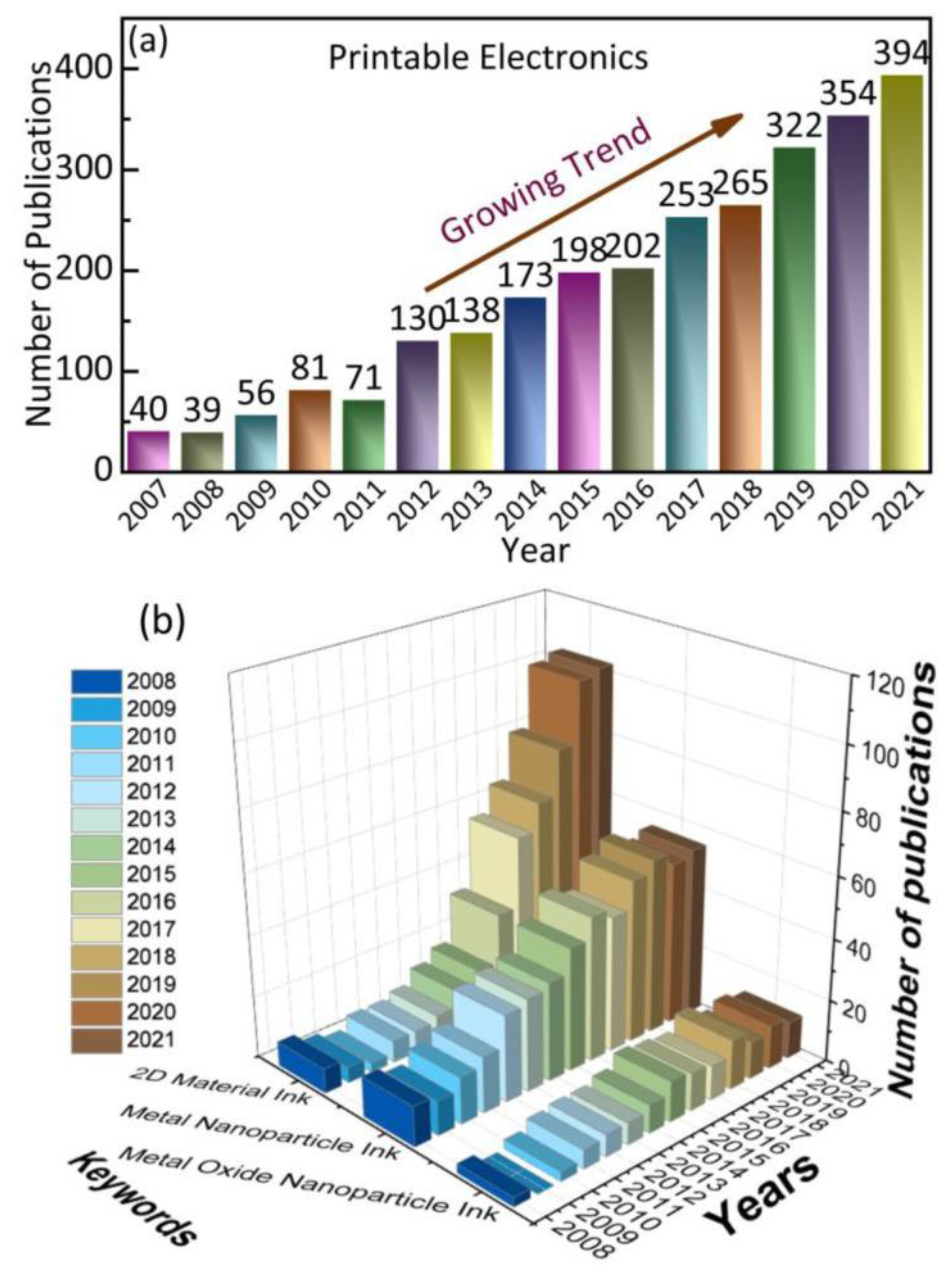
Figure 2.
Printing technologies using conducting ink (a) inkjet printing; (b) aerosol printing; (c) extrusion-based printing; and (d) electrohydrodynamic printing.6 (Images and captions are used without changes from the reference6, under Creative Commons 4.0 License.7).
Figure 2.
Printing technologies using conducting ink (a) inkjet printing; (b) aerosol printing; (c) extrusion-based printing; and (d) electrohydrodynamic printing.6 (Images and captions are used without changes from the reference6, under Creative Commons 4.0 License.7).
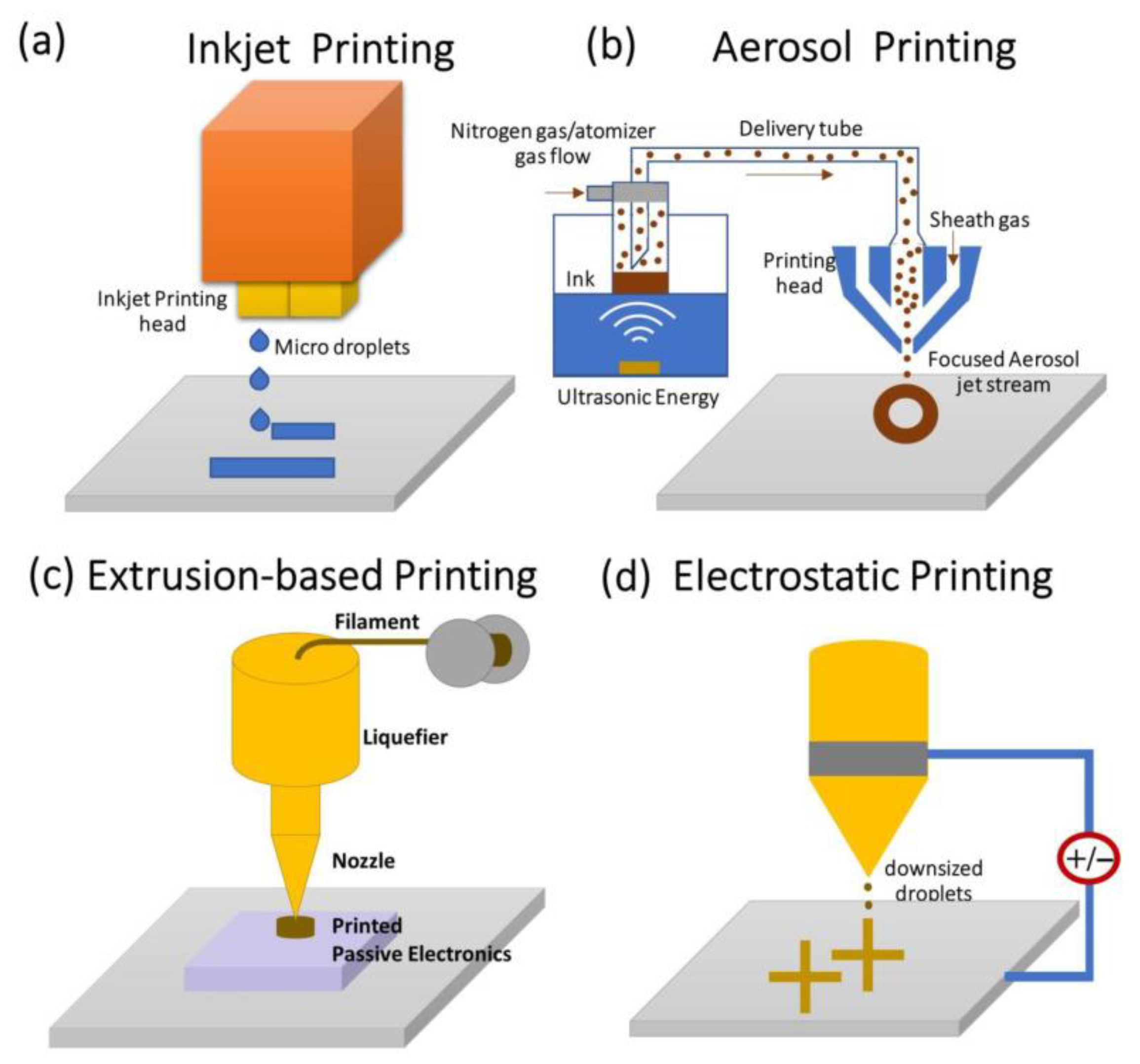
Figure 3.
Top: Schematic illustration depicting the steps entailed in the fabrication of the SC. Bottom: Charge storage mechanism in CHBAC electrode. (CHBAC refers to catechin-grafted activated carbon; SC for supercapacitor; images and captions are used without changes from reference29, under Creative Commons 4.0 License.7).
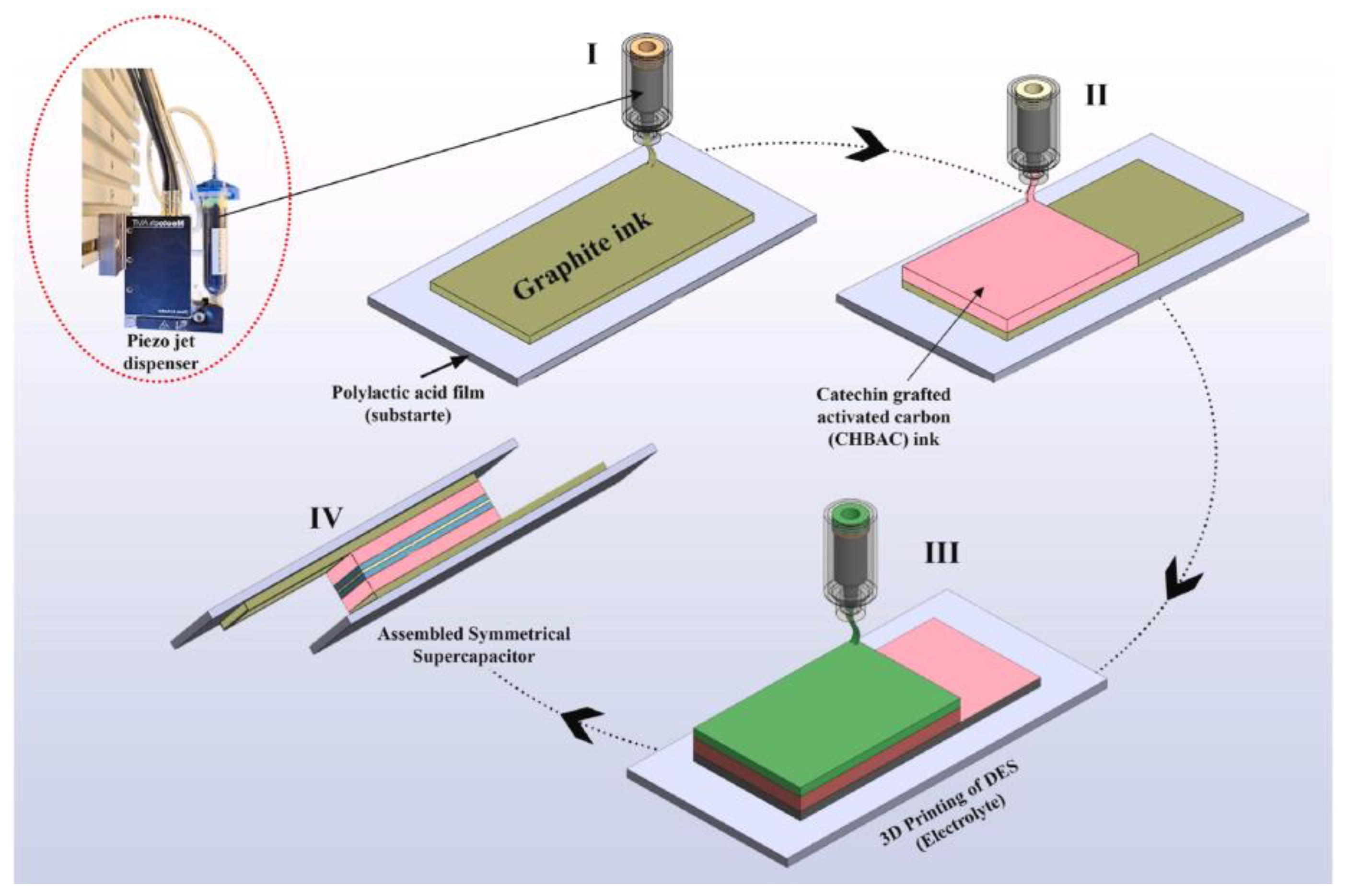
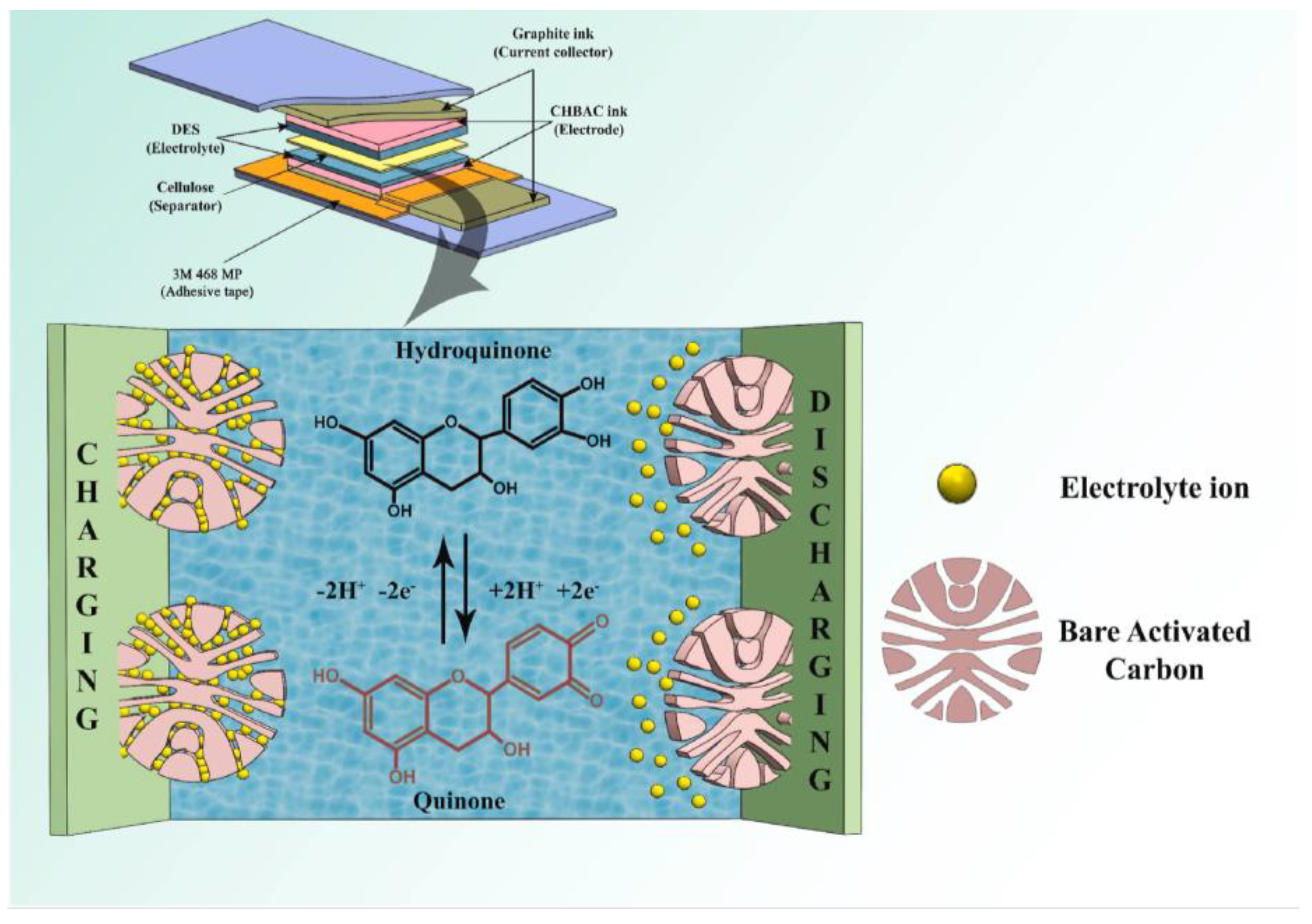
Figure 4.
Top: Interdigital conductive ABS sensor (a) structural layout (b) front view of fabricated sensor (c) back view of fabricated sensor (W = 4 mm, L1 = 65 mm, L2 = 70 mm and g = 2 mm). Bottom: Salt and sucrose concentration sensing. (Images and captions are used without changes from reference33, under Creative Commons.34).
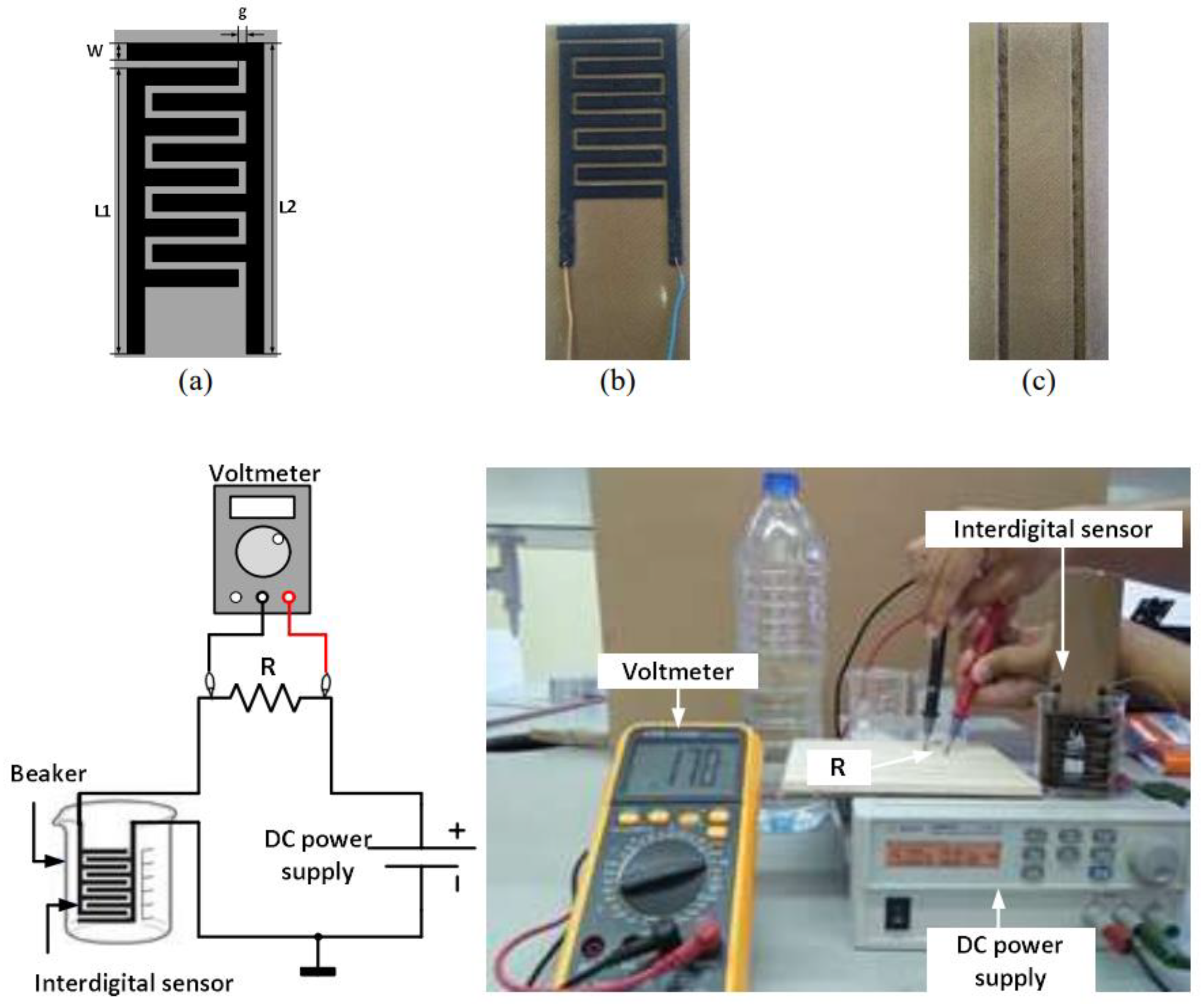
Figure 5.
Field of application of optimization in the 48 publications selected from the relevant literature66 (The image and caption are used without changes from the reference66, under Creative Commons 4.0 License.7).
Figure 5.
Field of application of optimization in the 48 publications selected from the relevant literature66 (The image and caption are used without changes from the reference66, under Creative Commons 4.0 License.7).
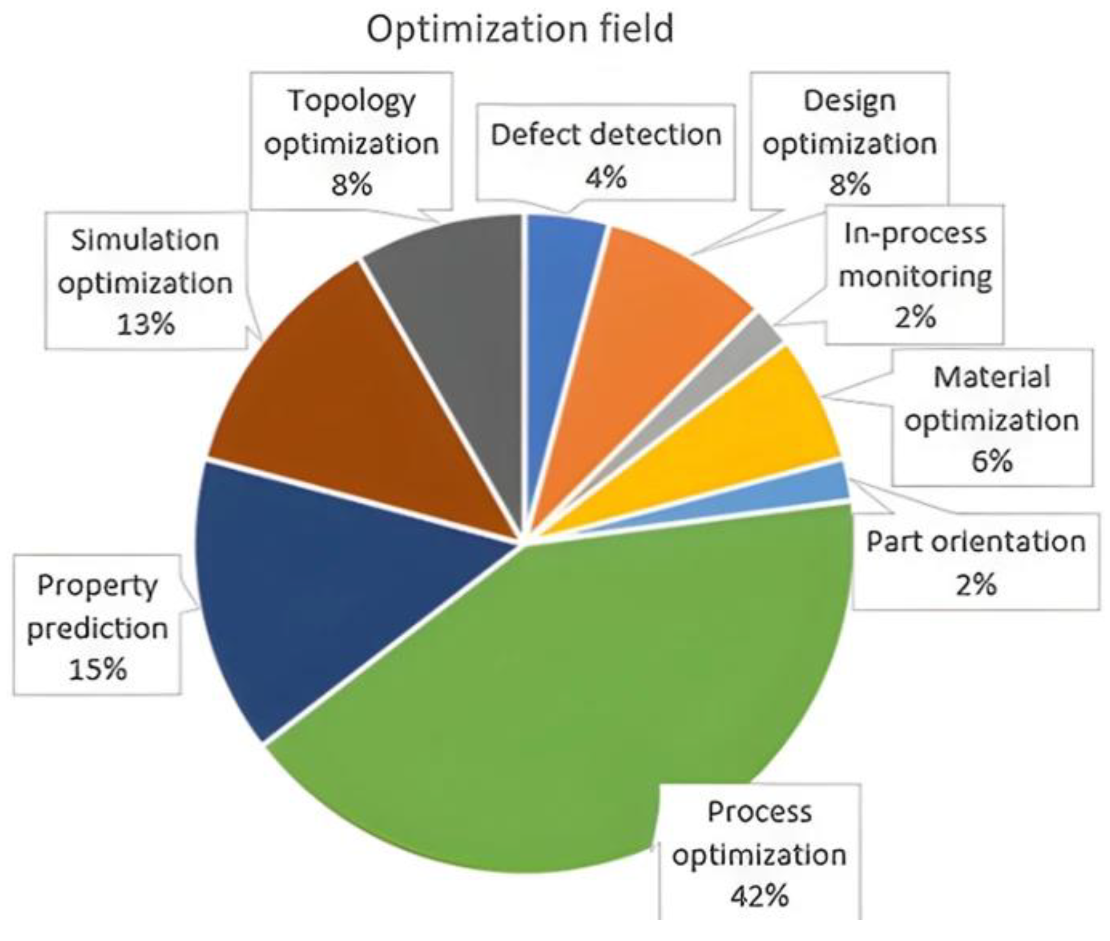
Figure 6.
Schematic example of the ANN67 (The image and caption are used without changes from the reference67, under Creative Commons 4.0 License.7).
Figure 6.
Schematic example of the ANN67 (The image and caption are used without changes from the reference67, under Creative Commons 4.0 License.7).
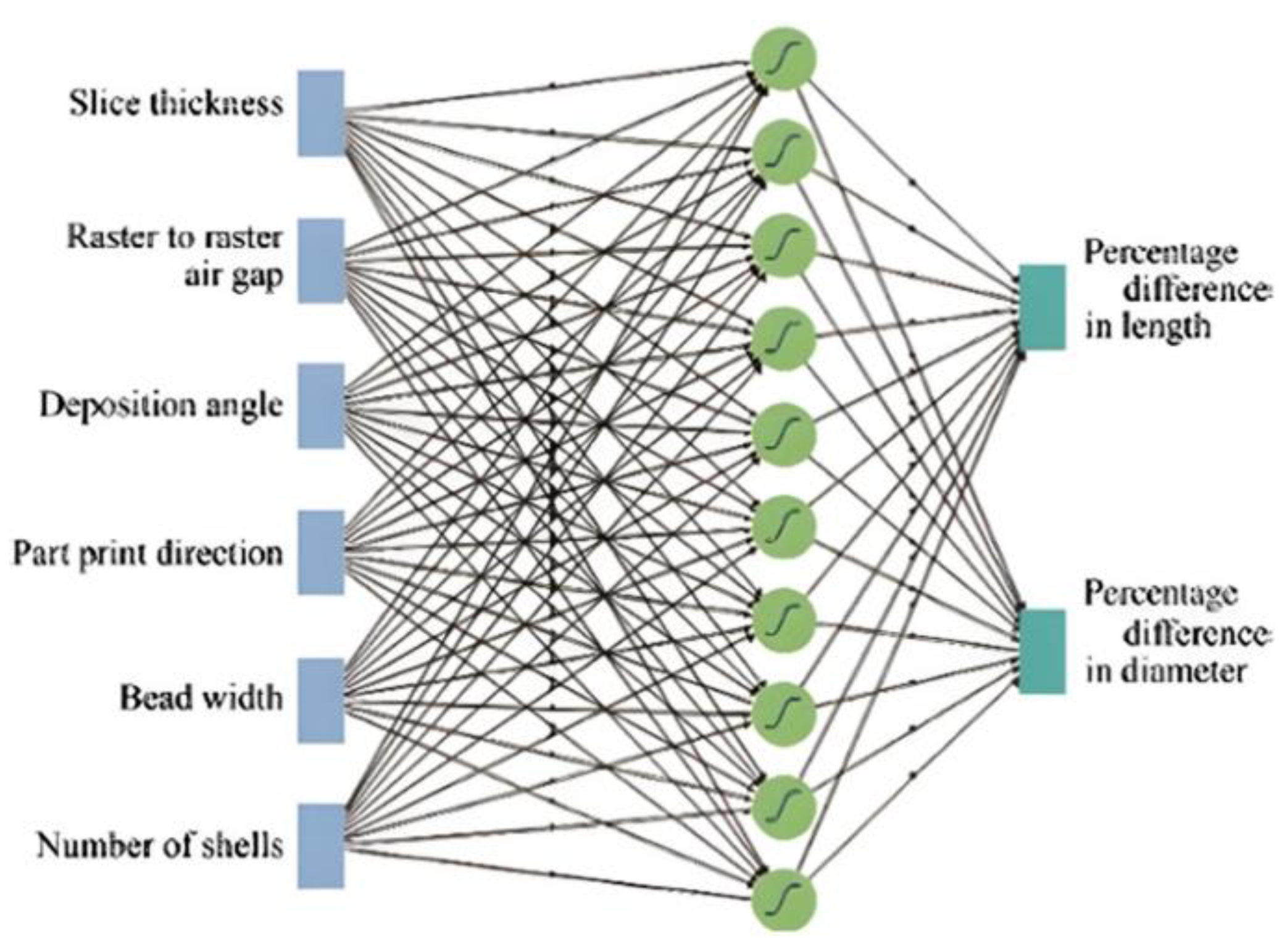
Figure 7.
AI methodologies applied in the 48 publications selected from the relevant literature66 (The image is used without changes from the reference66, under Creative Commons 4.0 License.7).
Figure 7.
AI methodologies applied in the 48 publications selected from the relevant literature66 (The image is used without changes from the reference66, under Creative Commons 4.0 License.7).
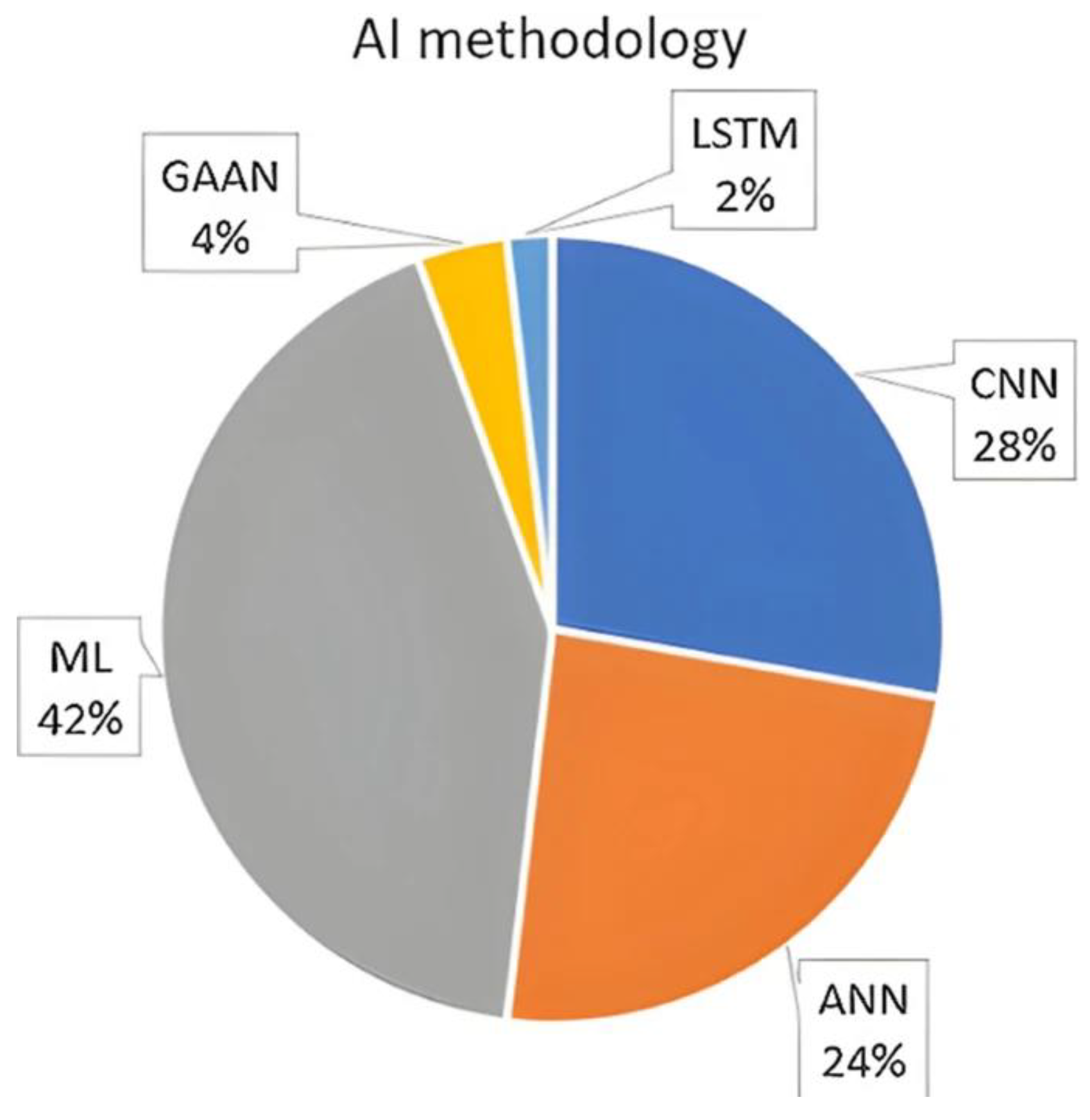
Figure 8.
BEAR for studying the mechanics of additively manufactured components.
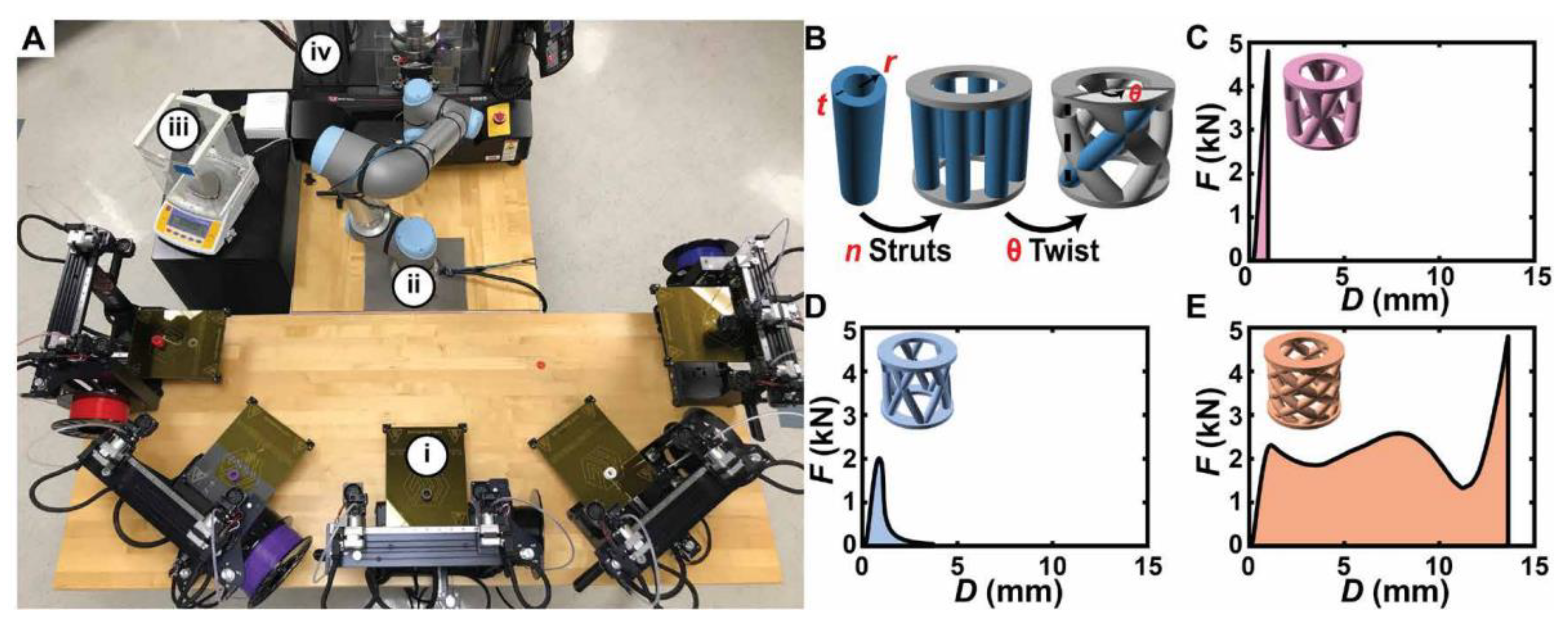
Figure 9.
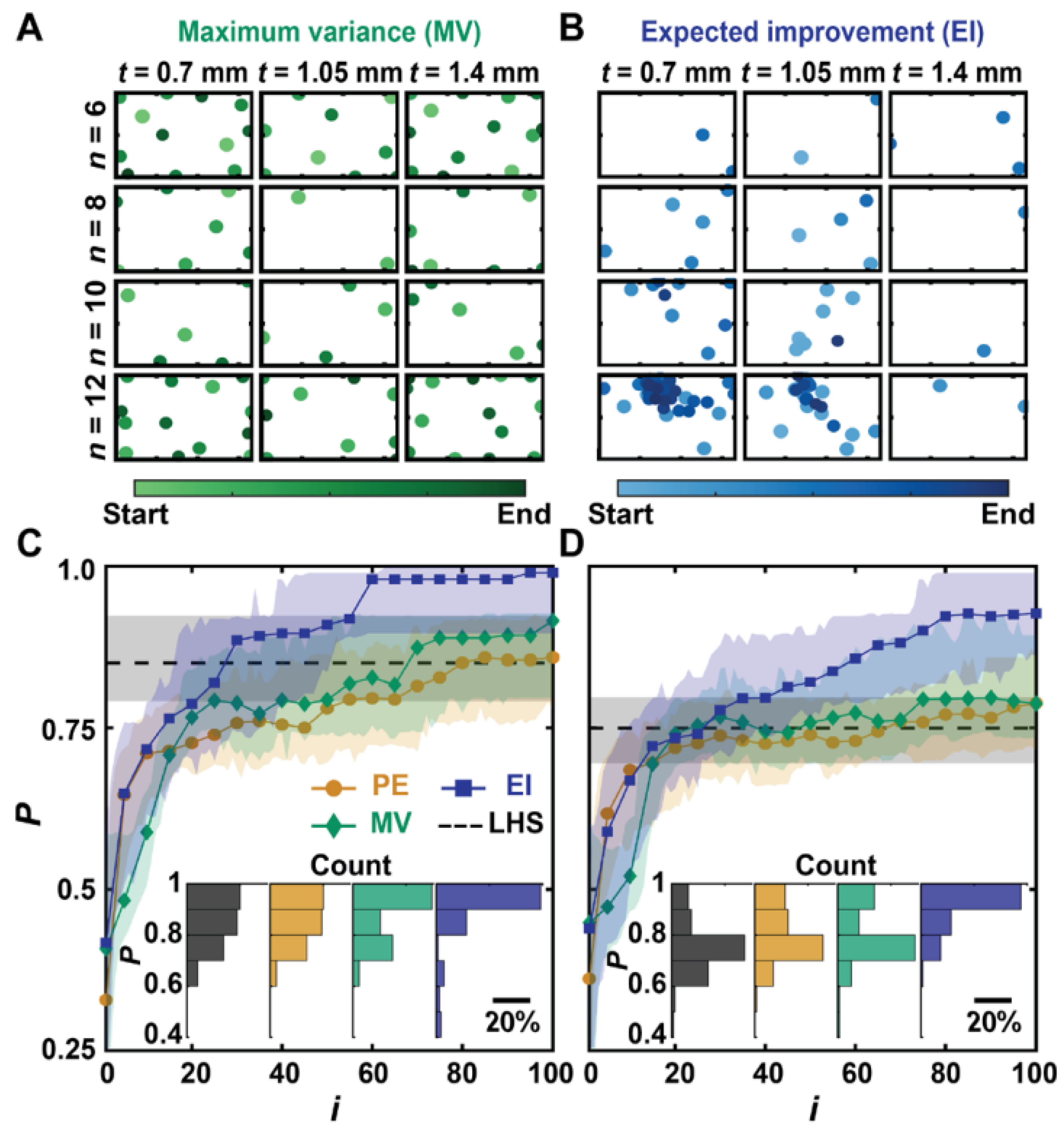
Simulated learning using BO. Distribution of experimental points when guided using (A) MV and (B) EI decision-making policies. The color gradient indicates the start and end of the campaign. Performance P versus experiment number i of simulated Bayesian campaigns with noise added to each simulated measurement drawn from a zero-mean Gaussian with (C) SD σ = 0.1 J and (D) σ = 5 J. EI- and MV-guided campaigns are benchmarked against PE and the average result of selecting 100 experiments using Latin hypercube sampling (LHS). Shaded regions correspond to the middle two quartiles of 100 simulated campaigns. The inset bar charts show the distribution in P at i = 100.(Figure and Caption from reference69 without change, under Creative Commons Attribution 4.0 International License.7).
Figure 9.
Simulated learning using BO. Distribution of experimental points when guided using (A) MV and (B) EI decision-making policies. The color gradient indicates the start and end of the campaign. Performance P versus experiment number i of simulated Bayesian campaigns with noise added to each simulated measurement drawn from a zero-mean Gaussian with (C) SD σ = 0.1 J and (D) σ = 5 J. EI- and MV-guided campaigns are benchmarked against PE and the average result of selecting 100 experiments using Latin hypercube sampling (LHS). Shaded regions correspond to the middle two quartiles of 100 simulated campaigns. The inset bar charts show the distribution in P at i = 100.(Figure and Caption from reference69 without change, under Creative Commons Attribution 4.0 International License.7).
Disclaimer/Publisher’s Note: The statements, opinions and data contained in all publications are solely those of the individual author(s) and contributor(s) and not of MDPI and/or the editor(s). MDPI and/or the editor(s) disclaim responsibility for any injury to people or property resulting from any ideas, methods, instructions or products referred to in the content. |
© 2025 by the authors. Licensee MDPI, Basel, Switzerland. This article is an open access article distributed under the terms and conditions of the Creative Commons Attribution (CC BY) license (http://creativecommons.org/licenses/by/4.0/).
Copyright: This open access article is published under a Creative Commons CC BY 4.0 license, which permit the free download, distribution, and reuse, provided that the author and preprint are cited in any reuse.


