
Submitted:
12 February 2025
Posted:
12 February 2025
You are already at the latest version
Abstract
With the rapid development of high-speed imaging, aerospace, and telecommunications, high-performance photodetectors across a broadband spectrum are urgently demanded. Due to abundant surface configurations and exceptional electronic properties, two-dimensional (2D) materials are considered as ideal candidates for broadband photodetection applications. However, broadband photodetectors with both high responsivity and fast response time remain a challenging issue for all the researchers. This review paper is organized as follows. Section I introduces the fundamental properties and broadband photodetection performances of transition metal dichalcogenides (TMDCs), perovskites, topological insulators, graphene, and black phosphorus (BP). This section provides an in-depth analysis of their unique optoelectronic properties and probes the intrinsic physical mechanism of broadband detection. In Section II, some innovative strategies are given to expand the detection wavelength range of 2D material-based photodetectors and enhance their overall performances. Among them, chemical doping, defect engineering, heterostructure construction, and strain engineering way are found to be mor effective for improving their photodetection performances. The last section addresses the challenges and future prospects of 2D material-based broadband photodetectors. Furthermore, to meet the practical requirements for very large-scale integration (VLSI) applications, their work reliability, production cost and compatibility with planar technology should be paid much attention.
Keywords:
2D materials
; broadband photodetection
; enhancing photodetection performance
; photoresponse mechanism
1. Introduction
With the rapid advancement of information technology, there is an increasing demand for photodetectors capable of covering a wide spectral range from visible to infrared light and even terahertz [1,2,3]. These detectors play an important role in aerospace exploration, remote sensing [4,5,6,7], environmental monitoring [8,9,10,11], and high-speed imaging [12,13,14,15]. Over the past decades, the narrow-bandgap compound semiconductors like mercury cadmium telluride (HgCdTe), indium antimonide (InSb) and silicon have been intensively researched due to their optimal bandgaps, which inherently keep them from broadband photodetection applications [16,17,18]. Although traditional photodetectors have made some progress, they still encounter some limitations [19,20]. For instance, HgCdTe photodetectors require a low operation temperature below 70 K to achieve high-performance detection. Moreover, they are not friendly to the environmental due to the existence of heavy metal elements Hg and Cd, and their fabrication process is complicated and expensive.
Two-dimensional(2D) materials such as transition metal dichalcogenides (TMDCs) [21,22,23,24], perovskite [25,26,27], graphene [28,29,30], topological insulators [31,32,33], black phosphorus (BP) [34,35] and MXenes [36,37,38] attract tremendous interest owing to their distinctive physical and chemical properties. 2D materials exhibit tunable bandgaps [39,40], strong light-matter interactions [41], high carrier mobility [42], and exceptional mechanical flexibility [43,44], enabling them with outstanding performances in broadband photodetection. For example, Hu et al. [45] achieved an ultra-broadband photoresponse ranging from ultraviolet to long-wave infrared (375 nm-10 μm) by integrating ferroelectric materials with pyroelectric functionality and low-dimensional semiconductor materials. Using the electric field reversible modulation characteristics of bipolar 2D van der Waals (vdW) heterojunctions, Zhai et al. [46] utilized to implement wide-spectrum (365-980 nm) convolution processing and recognition within sensors. Zhang et al. [47] designed an innovative 2D vertical heterostructure photodetector with an exceptionally high optical responsivity and detectivity over a broad wavelength range (405-1550 nm). Despite there are some research progresses in 2D material-based photodetectors, fabrication of high-performance broadband photodetectors with both rapid switching speed and large photoresponsivity is still challenging due to the limitation of photosensitive materials themselves, such as low carrier mobility, high dark current, low light absorption efficiency, and poor environmental stability. Additionally, the photoresponse speed and detection spectral range of these photodetectors are often affected by carrier recombination, trap states, or material crystallinity. Therefore, modulation of the optoelectronic properties of 2D materials and fabricate high-performance photodetector are very essential for their actual application in broadband photodetection.
The purpose of this review is to provide a comprehensive perspective, which analyzes and summarizes recent research strategies for enhancing the work performances of 2D material-based devices for broadband photodetection. First, the optoelectronic properties of individual 2D materials are introduced to explore the intrinsic broadband photodetection mechanism. Next, the strategies for enhancing the work performance of 2D material-based photodetectors will be discussed in detail. Finally, we will address the challenges of realizing high-performance broadband photodetectors and their potential applications in future.
2. Individual 2D Material-Based Broadband Photodetectors
For broadband photodetection, individual 2D materials rely on two principal physical mechanisms: the photo-thermoelectric effect and photoconductivity effect. The photo-thermoelectric effect describes the change in a material's resistance due to thermal effects, resulting in a measurable resistance change. On the other hand, the photoconductivity effect refers to the creation of electron-hole pairs following the absorption of photons with energy above the material's bandgap, enhancing electrical conductivity and allowing light detection across a broad spectral range. Devices predominantly governed by the photo-thermoelectric effect can achieve an exceedingly broad detection spectrum, extending from the visible to the near-infrared, mid-infrared, far-infrared regions, and even terahertz waves. In contrast, devices of photoconductive effect are restricted to a more defined wavelength range, depending on their bandgap width. In this section, the properties of five commonly-used 2D materials are explored for realizing broadband photodetection: transition metal dichalcogenides (TMDCs), graphene, black phosphorus (BP), topological insulators, and perovskites [48,49,50].
2.1. Transition Metal Dichalcogenides
Transition Metal Dichalcogenides (TMDCs) are layered materials consisting of a layer of transition metal atoms (molybdenum (Mo) or tungsten (W)), sandwiched between two layers of chalcogen atoms (sulfur (S), selenium (Se), or tellurium (Te)). These materials are characterized by the chemical formula MX2, where M represents the transition metal and X denotes the chalcogen. A key feature of TMDCs is their bandgap, which is significantly influenced by the number of layers, thereby conferring upon them a broad spectral response capability. The sensitivity of TMDCs to layer thickness endows them with the ability to absorb a broad spectrum of light, rendering them highly desirable for applications in broadband photodetection.
For instance, Pargam et al. [51] developed a 2D SnSe thin films photodetector capable of detecting light from 400 to 1200 nm owing to its narrow bandgap, maintaining stable performance even after 30 days of air exposure. Guo et al. [52] fabricated a high-performance photodetector using high quality ternary Ta2NiSe5 nanosheets (Figure 1a), featuring a narrow bandgap of 0.25 eV. As illustrated in Figure 1b, the device exhibits broadband photodetection capabilities across the visible to infrared (IR) spectral (405-2200 nm) at room temperature. At 405 nm, it achieves a maximum responsivity of up to 280 A/W. Notably, at 2200 nm, it exhibits an impressive responsivity of 63.9 A/W and a detectivity of 3.8 × 10⁹ Jones, as shown in Figure 1c. Ren et al. [53] synthesized a high-quality 2D Bi2O2Se thin film on a SrTiO3 substrate via chemical vapor deposition (Figure 1d), exhibiting an perfect atomic arrangement and a well-defined interface with the substrate. As illustrated in Figure 1e-g, a photodetector based on the 2D Bi2O2Se thin film was developed to detect across ultraviolet, visible, and infrared wavelengths from 365 to 940 nm. It demonstrates rapid response time of 32 ms and 44 ms, a peak response sensitivity of 136 mA/W, and a detectivity up to 2×10⁹ Jones. Moreover, the Bi2O2Se photodetector shown remarkable stability performance in ambient atmosphere after one year storage, as demonstrated in Figure 1h.
2.2. Two-Dimensional Perovskite
In addition to conventional 2D materials like TMDCs, 2D perovskite materials are also emerged in broadband photodetectors [54,55]. Perovskite materials have a crystal structure of ABX3, where A is typically an organic molecule or alkali metal ion, B is a transition metal ion, and X is a halogen ion. They have attracted significant interest in broadband photodetection due to their remarkable optical properties, including tunable bandgap [56,57] and excellent charge carrier performance [58].
Li et al. [59] synthesized a stable 2D Cs0.05MA0.45FA0.5Sn0.5Pb0.5I3(Sn-Pb) perovskite, with reduced Sn vacancy density and suppressed yellow phase impurities through Sn2+ enrichment Cs+ ions incorporation. As given in Figure 2a, the photodetector based on Sn-Pb perovskite exhibits a response range spanning from ultraviolet to near-infrared wavelengths (Figure 2b). Under irradiation with a 720 nm laser, the device demonstrated a responsivity of 0.29 A/W and achieved ultrafast response characteristics with rise and fall time of 2 μs and 12.1 μs, as shown in Figure 2c. Xu et al. [60] presented a novel flexible optoelectronic detector utilizing (BA)2(MA)Sn2I7, which achieved a wide-spectral response across the ultraviolet-visible-near-infrared spectrum from 365 to 1064 nm, as illustrated in Figure 2d and 2e. The device exhibited high responsivities of 28.4 A/W at 365 nm and 0.02 A/W at 1064 nm, corresponding to detectivities of 2.3×10¹⁰ and 1.8×10⁷ Jones, respectively. Furthermore, it demonstrated stable photodetection performance after 1000 bending cycles. Figure 2f shows that Mei et al. [61] employed a low-temperature vapor-diffusion method to synthesize 2D MAPbBr3 nanoplates photodetector. The high specific surface area and surface trap-assisted absorption characteristics of the nanoplates contribute to the device's outstanding performance in the near-infrared spectral ranging from 850 to 1450 nm, as depicted in Figure 2g. Notably, it achieves an external quantum efficiency (EQE) of 1200% and a detectivity of 5.37×10¹² Jones, while also demonstrating rapid response rise/fall time of 80/110 μs, as shown in Figure 2h and 2i. Xu et al. [62] investigated a broadband photodetector based on MAPbBr3 (Figure 2j), capable of spanning the ultraviolet to near-infrared spectral range. Figure 2k presents a schematic diagram of the photo-responsive mechanism. The mechanism for photocurrent generation in the visible light spectrum was elucidated as the photoelectric effect. For incident light wavelengths shorter than the cutoff wavelength of 574 nm, single-photon absorption serves as the primary absorption mechanism. In contrast, for wavelengths exceeding 574 nm, sub-gap trap state absorption predominates. In the near-infrared region, thermal effects govern the photoresponse mechanism. Figure 2l illustrates the device's optical response across various wavelength bands, revealing that it attains a high plateau prior to reaching a wavelength of 520 nm.
2.3. Graphene
Graphene, a 2D material composed of carbon atoms arranged in an sp² hybridized configuration, forms a planar hexagonal lattice structure [63]. It exhibits zero bandgap semi-metallic characteristics, which means that the energy required for electrons to transition from the valence band to the conduction band is minimal. This allows graphene to absorb a wide range of photon energies across the spectrum [64]. Additionally, the linear dispersion of Dirac electrons in graphene suggests that for any excitation, there is always a resonance of an electron-hole pair, contributing to its high bandwidth photodetection capability. Combined with graphene's exceptionally high electron mobility, these properties enable it to rapidly generate photocurrents in response to light, making it an ideal material for broadband photodetection.
Liu et al. [65] reported an ultra-broadband photodetector based on a graphene bilayer heterostructure, with the device structure illustrated in Figure 3a. Under illumination, the top layer generates hot carriers that tunnel into the bottom layer, resulting in charge accumulation at the gate and producing a pronounced optoelectronic gating effect on channel conductivity. This device demonstrates room-temperature light detection across a spectral from visible to mid-infrared wavelengths, achieving a mid-infrared responsivity exceeding 1 A/W, as shown in Figures 3b and c. However, due to the inherently low optical absorption of graphene, the responsivity of graphene-based photodetectors is relatively low. Yang et al. [66] developed a novel method for the preparation of highly conductive reduced graphene oxide (rGO) and constructed a fully suspended photodetector as illustrated in Figure 3d. This detector displayed the fastest and broadest optical response among all reported rGO photodetectors. As demonstrated in Figures 3e and f, the response time is approximately 100 ms, with a response range spanning from ultraviolet to terahertz spectral region. Qasim et al. [67] established a high-performance, self-powered broadband photodetector, as illustrated in the Figure 3g. This device is constructed from a stack formed on an n-Si substrate by graphene. As illustrated in Figure 3h, the device exhibits a remarkable broadband spectral response ranging from visible light (405 nm) to infrared (1,550 nm). This phenomenon can be attributed to the formation of a Schottky barrier at the interface between graphene and silicon. Under illumination, photons with energies below the silicon bandgap are absorbed, generating photo-induced charge carriers that are subsequently separated by the built-in electric field, resulting in photogenerated current. Under illumination at 532 nm and with a rapid rise time of 320 µs, the device achieves a responsivity of 300 mA/W, a detectivity of 3.37 × 10¹¹ Jones, and an external quantum efficiency of 90%, as depicted in the Figure 3i. Our team has proposed an asymmetric plasmonic nanostructure array on planar graphene [68], as illustrated in the Figure 3j. Under excitation, the non-centrosymmetric metallic nanostructures exhibit a strong light-matter interaction with the local field near the tip surface, resulting in an asymmetric electric field. These characteristics can enhance the generation of hot electrons within graphene, leading to directed diffusion currents. As shown in Figure 3k, the device demonstrates significant optical responsiveness across a wavelength range of 0.8 to 1.6 µm. Under laser excitation at 1.4 µm and zero bias, it achieves a responsivity of 25 mA/W and a noise equivalent power of about 0.44 nW/Hz1/2.
2.4. Topological Insulators
Topological insulators, with their bulk exhibiting narrow band gaps and their surfaces featuring zero band gaps, possess surface states that connect the conduction and valence bands of the bulk, enabling broad spectral range detection [69]. The unique electronic structure of topological insulators, characterized by their robust topologically protected surface states, is the cornerstone of their potential for wide-spectrum photodetection. These surface states are impervious to backscattering and non-magnetic impurities, thereby ensuring efficient charge transport and light absorption across a diverse spectral of wavelengths.
Liu et al. [70] constructed a Bi2Se3 nanowire/Si photodetector, as illustrated in Figure 4a, showing exceptional photoelectric detection performance. Due to its small bulk bandgap, the device covers a wide spectral range for photodetection, spanning from 380 to 980 nm as detailed in Figure 4b. Moreover, an effective Schottky barrier is established at the interface. When subjected to varying optical power excitation at a wavelength of 808 nm, the device consistently shows favorable photocurrent responses, achieving a peak responsivity of 103 A/W and a swift response time of around 45 ms, as given in Figure 4c. Chen et al. [71] introduced a super-broadband photodetector that integrates dual mechanisms based on the topological insulator Sb2Te3, as revealed in Figure 4d. The response range of this photodetector spans from 520 nm to 0.28 THz (as shown in Figure 4e). Upon irradiation with a 520 nm laser, the device demonstrates a room-temperature responsivity of 114.6 mA/W and a detectivity of 1.78 × 108 cm² Hz1/2 W-1. At a frequency of 0.12 THz, the room-temperature responsivity is 38.5 mA/W, with a detectivity of 3.44 × 1010 cm² Hz1/2 W-1, and an observed response time of 20 ps. As presented in Figure 4f, the device's operation in the visible to infrared spectrum is primarily due to the photoconductive effect, while its terahertz functionality is largely attributed to the asymmetric scattering behavior of topological surface states. Lai et al. [72] reported a wide-spectrum photodetector based on TaIrTe4, with its device structure shown in Figure 4g. The photodetector demonstrated a broadband response from 532 nm to 10.6 μm, as seen in Figure 4h, suggesting that its detection range can be extended into the far-infrared and terahertz regions. Furthermore, the anisotropic response of the TaIrTe4 photodetector was quantified, showing that the degree of anisotropy escalates as the excitation wavelength approaches the Weyl node.
2.5. Black Phosphorus
Black phosphorus (BP), a stable allotrope of phosphorus in air, is a typical layered two-dimensional material. Each layer consists of corrugated atomic chains, where each atom engaging in sp3 hybridization to form non-planar six-membered ring structures with three neighboring atoms. This material exhibits direct bandgap semiconductor characteristics, with the bandgap narrowing from 1.7 eV in monolayers to 0.3 eV in bulk forms as the number of layers increases [73,74]. Capitalizing on its narrow bandgap, BP has been widely applied in broadband photodetection.
Huang et al. [75] developed a black phosphorus photodetector, as depicted in the Figure 5a, which demonstrated high-performance detection across the 400-900 nm spectrum with a remarkable responsivity up to 106 A/W level, as revealed in Figure 5b. Another BP photodetector developed by Guo et al. [76] and shown in Figure 5c, achieved a responsivity of 82 A/W under 3.39 μm laser irradiation. Xu et al. [77] fabricated a BP photodetector enables mid-infrared photodetection from 2.5 to 3.7 μm wavelengths. Ryan et al. [78] designed a photodetector illustrated in Figure 5d that leverages the light guiding effect of black phosphorus for effective detection from near-infrared to mid-infrared (1.56-3.75 μm). This device exhibited an ultrafast response time of 65 ps when excited by a 3.6 μm laser irradiation, as given in Figures 5e and 5f. The performance of some broadband photodetectors based on individual 2D materials are summarized in Table 1.
3. Strategies for Enhancing Photodetection Performances
As previously mentioned, devices based on individual 2D materials for broadband photodetection have been extensively discussed. Despite notable progress, their performance has yet to fully meet current requirements. Therefore, researchers have devoted considerable effort to developing innovative techniques and strategies to enhance the photodetection performance of these devices. Such methodologies include chemical doping to alter electronic properties, defect engineering to modulate carrier concentrations, heterostructure fabrication to create synergistic effects, and strain engineering to tune bandgaps and enhance light-matter interactions (Figure 6). These strategies are crucial for enhancing the functionality and efficiency of 2D material-based broadband photodetectors, ensuring they can meet the demanding requirements of practical applications.
3.1. Chemical Doping
Chemical doping is a strategy employed to fine-tuning the band structure and carrier density in semiconductor materials by incorporating impurity atoms or molecules [93,94], thereby enabling broadband photodetection. Peng et al. [95] synthesized a PbSe0.5Te0.5 atomic film through the incorporation of Te into PbSe, which resulted in a reduced bandgap and enhanced carrier mobility, leading to exceptional photo-response and broad-spectral detection capabilities as shown in Figure 7a. The doped PbSe0.5Te0.5 photodetector displays superior broadband photodetection performance (405-5000 nm), which attributed to its narrow band gap (Figure 7b and 7c). Parth et al. [96] synthesized a range of metal-doped SnS materials (Fe, Mg, Mn, Pd, W) via the hydrothermal method. Interestingly, Mg-doped SnS demonstrated the most pronounced response in both visible and near-infrared spectra among the various metal-doped SnS variants, as observed in Figure 7d and 7e. By modulating the energy band through Mg doping, the 7% Mg-doped SnS demonstrated excellent photo responsivity in the visible-infrared spectral, as seen in Figure 7f-g. Additionally, Parth et al. [97] effectively doped in into SnS to facilitate broad-spectrum photodetection ranging from 400 nm to 1100 nm by altering the bandgap from 1.44 eV to 2.08 eV . Through density functional theory calculations, Zhao et al. [98] investaged that the synergistic effect of vanadium substitution doping and molybdenum vacancies not only diminishes the bandgap but also enhances light absorption in monolayer MoSe2, as illustrated in Figure 7h. They successfully fabricated a photodetector based on monolayer MoSe2 with 6% V and Mo vacancies, which displayed a broadband spectral response from 365 nm to 2240 nm, and the photoresponsivity reached 9.7 A/W and 2.8 mA/W at 520 nm and 2240 nm, respectively (Figure 7i). Using the CVD method, our team [99] synthesized high-quality single-crystal (GaN)1-x(ZnO)x nanobelts and fabricated a wide-spectral ultraviolet-visible photodetector as illustrated in the Figure 7j. The photodetector exhibited remarkable responses across the ultraviolet to visible light spectral, thanks to its excellent optical response and tunable bandgap. As shown in the Figure 7k and 7l, under 365 nm ultraviolet irradiation, the device exhibited a responsivity of 2.8×10⁵ A/W. Under 532 nm visible light irradiation, the device achieved a response time of 480 ms with a responsivity of 1.9×10⁴ A/W.
3.2. Defect Engineering
Defects such as vacancies, edges, grain boundaries, and substitutional impurities inherently present in 2D materials significantly influence their electronic and optoelectronic characteristics. By employing defect engineering strategies, these defects can be deliberately controlled and optimized, enhancing the performance of 2D material-based devices and overcoming the limitations imposed by their inherent bandgap. This approach has the potential to noticeably enhance the responsivity, response speed, and operational wavelength range of photodetectors, expanding their capabilities in optoelectronic applications. Wu et al. [100] developed WS2/Ge heterojunction photodetectors through defect engineering and interface passivation techniques, as shown in Figure 8a. The WS2/AlOx/Ge photodetector demonstrates exceptional performance attributed to a reduced bandgap resulting from defects. It exhibits a high responsivity of 634.5 mA/W, a detectivity of 4.3×10¹¹ Jones, rapid response times, and an extensive spectral response ranging from 200 nm to 4.6 µm, as found in Figure 8b and 8c. Furthermore, this device exhibits remarkable MWIR imaging capabilities at room temperature. Xie et al. [101] achieved room-temperature THz photodetection in MoS2 by conducting bandgap engineering through the introduction of Mo4+ and S2- vacancies. The generation and transport of excess charge carriers in the MoS2 sample are regulated by the vacancy concentration and resistivity in the THz electromagnetic radiation. A photo responsivity at 2.52 THz with 10 mA/W was achieved by balancing the fluctuation of carrier concentration and the scattering probability of charge carriers in the MoS2.19 sample.
In contrast to the bandgap modulation, defects also can act as efficient charge traps, achieving exceptional photocurrent gain in broadband photodetectors. Cao et al. [102] proposed a macro-assembled graphene nanofilm with precisely controlled defect states for wide-band infrared detection, investigating the correlation between the concentration of material defect states and detection performance. The device architecture is illustrated in Figure 8d. Defect states re-enter the conduction band (CB) and valence band (VB) within the D-nMAG trapped charge carriers for thermalization, resulting in enhanced photocurrent gain. Figure 8e presents the responsivity of various defect state concentrations of D-nMAG in the near-infrared (NIR) region at 900 nm, while Figure 8f displays the responsivity in the mid-infrared (MIR) region at 4 µm. Duan et al. [103] introduced a Ni/MoS2 photodetector, as illustrated in Figure 8g. This detector is modified with nickel nanoparticles on MoS2 that contains S vacancies, achieving excellent photodetection performance through defect engineering. The introduction of S vacancies enables effective light detection in the near-infrared range. Additionally, the photocatalytic effect of the nickel nanoparticles within the device reduces recombination rates and enhances hole transport. Figure 8h illustrates the schematic representation of the energy band structure under this configuration, thereby improving both the sensitivity and response speed of the photodetector. The MoS2 photodetector modified with nickel nanoparticles demonstrates responsivity of 106.21 A/W and 1.38 A/W under 532 nm and 980 nm light, with detectivity of 1.9×10¹² Jones and 8.9×10⁹ Jones, respectively, as revealed in Figure 8i.
3.3. Heterostructure Construction
2D materials' lack of dangling bonds on their surfaces provides exceptional flexibility in integrating with materials of other dimensions, including 0D, 1D, 2D and 3D, without strict lattice matching requirements. This flexibility expands the possibilities for engineering diverse device architectures. By selectively combining complementary materials to form heterostructures, synergistic effects and functionalities surpassing those of individual components can be achieved, leading to significantly improved device performance and opening up new horizons for the design and novelty of photodetectors.
As presented in Figure 9a, Kolli et al. [104] utilized CVD method to grow monolayer MoS2 on the SiO2/Si substrate and employed a cost-effective solution processing method to synthesis SnS2 quantum dots (QDs). This strategy resulted in the creation of a 0D/2D SnS2-QDs/monolayer MoS2 photodetector. The integration of SnS2 QDs with the monolayer MoS2 not only boosted the device's performance but also expanded its spectral response to the ultraviolet region. Figure 9b shows that the device achieves responsivities of approximately 278 A/W, 435 A/W, and 189 A/W in the ultraviolet, visible light, and near-infrared regions, respectively. The superior performance of this photodetector is largely due to the band bending and built-in potential at the SnS2 QDs/MoS2 interface (as shown in Figure 9c), which enhances carrier injection and separation efficiency under optical excitation. Moreover, the hybrid dimensional structure effectively minimizes the dark current in the photodetector. To overcome the limitations of long response time and low light responsiveness associated with one-dimensional ZnO, our team [105] constructed a MoS2-on-ZnO vertical heterojunction photodetector, as illustrated in Figure 9d. As shown in Figure 9e, under ultraviolet (UV) irradiation, the photodetector achieves a remarkable responsivity of 273 A/W with a response speed of less than 24 ms. Furthermore, the MoS2-on-ZnO heterojunction photodetector also exhibits excellent visible light response, achieving a high responsivity of 74 A/W and rapid response speed (<24 ms) under irradiation by a 650 nm laser. Figure 9f presents the energy band structure of this heterostructure under UV and visible light excitation. The ZnO nanowires possess high carrier mobility that enables them to respond effectively to UV light while providing a fast carrier transport pathway. Meanwhile, the MoS2 layer serves as an optical control layer that respond to visible light and facilitates the transfer of photo-generated electrons into the ZnO nanowires to modulate their conductivity. Duan et al. [106] fabricated a 2D/2D self-powered photodetector based on a multilayer MoSe2/FePS3 heterojunction, as shown in Figure 9g. The device exhibits significant optical response across the wavelength range of 350 to 900 nm, with maximum Rmax and EQEmax reaching 52 mA/W and 12%, respectively, at a wavelength of 522 nm, as shown in Figure 9h. This excellent performance is attributed to the type-II band alignment in the MoSe2/FePS3 van der Waals heterojunction, which creates a built-in electric field (Figure 9i). By utilizing wide direct bandgap (3.4 eV), high carrier mobility (approximately 1250 cm²/V·s), exceptional radiation hardness, and superior thermal conductivity of GaN, Liu et al. [107] designed a fully vertical 2D/3D van der Waals stacked p-MoxRe1-xS2/n-GaN heterojunction photodetector, demonstrating a high Ilight/Idark ratio of 1.48×10⁶, photoresponsivity of 888.69 A/W, impressive detectivity (D*) at 6.13×10¹⁴ Jones, and rapid response times with rise and fall durations of 181 ms and 259 ms (Figure 9j and 9k). The device's spectral response covers ultraviolet (UV), visible light, and near-infrared (NIR) regions through bandgap integration and modulation (Figure 9l).
As shown in Figure 10a, our team [108] has developed a van der Waals heterostructure photodetector based on InSe/Te. Figure 10b indicates that this photodetector, which is based on type-I band alignment, allows the InSe component to selectively modulate the spectral response. The Te layer efficiently collects photo-generated holes from the InSe layer, suppressing the recombination of photo-generated carriers and thereby enhancing the device's optical responsivity and detection range. Figure 10c demonstrates that the device exhibits a broad spectral response from 400 to 1100 nm. Under illumination, the heterostructure device achieves an optical on/off ratio of up to 105 and a detectivity reaching as high as 1.77×10¹¹ Jones. Vashishtha et al. [109] constructed a MoS2/Sb2Se3 heterojunction photodetector (Figure 10d), where the two materials formed a type-II band alignment directly, as shown in Figure 10e. This alignment creates a small barrier potential at the MoS2/Sb2Se3 interface, minimizing the bending effect in the energy band diagram and significantly increasing the number of accessible states for charge carriers. This enhancement in charge carrier concentration substantially boosts the device's photoresponse, improving its efficiency in converting photonic energy into electrical response. Figure 10f illustrates the device's capability to function across the visible to infrared spectral range. As shown in Figure 10g, Yuan et al. [110] constructed a type-III band alignment GeSe/SnS2 van der Waals photodetector by utilizing the band structure alignment characteristics of GeSe and SnS2. As illustrated in Figure 10h, the heterostructure device of GeSe/SnS2 exhibits exceptional photodetection capabilities, including a broad spectral response across the ultraviolet-visible-near-infrared range (255-1920 nm). Under 255 nm laser irradiation, it demonstrates a high responsivity of 50.7 A/W, an impressive specific detectivity of 1.09 × 10¹⁰ Jones, and a rapid response time of 2.1 ms. The outstanding device performance and wide spectral sensitivity of the device can be attributed to its type-III electronic band structure arrangement. As depicted in Figure 10i, the formation of the heterostructure creates an internal electric field from SnS2 to GeSe, establishing a favorable environment for effective interlayer charge transfer.
3.4. Strain Engineering
The remarkable mechanical flexibility of 2D materials allows for the application of substantial strain, which in turn can significantly modify the electronic, optical, and transport properties of these materials. This strain-induced modulation of properties opens up new possibilities for optoelectronic device applications, paving the way for the development of innovative and high-performance devices [111,112,113]. Strain engineering enhances the performance of wide-spectral photodetectors by adjusting the band structure, light absorption, and charge carrier mobility of the materials [92,114,115].
Lu et al. [116] designed a strain-plasmonic coupled MoS2 photodetector by transferring a monolayer of MoS2 onto a pre-fabricated array of gold nanoparticles, as shown in Figure 11a. This design enables significant biaxial tensile strain, which narrows MoS2's wide bandgap and enhances light absorption of MoS2 due to the gold nanoparticles. Figure 11c shows the strain-plasmonic coupled photodetector exhibited an expanded detection range of 60 nm and a remarkable enhancement in signal-to-noise ratio by 650%, optimizing both detection range and responsivity. Wang et al. [117] demonstrated a MoS2/Sb2Te3 photodetector (Figure 11d) that exhibited substantial tunability under compressive strain of up to 0.3%. The strain at the heterojunction interface influenced the bandgap of MoS2/Sb2Te3, altering the heterojunction band structure and modulating the detector's optical absorption characteristics. Figure 11e illustrates the wide-spectral response range of the device, spanning from 500 to 900 nm. Under strain, the bandgap and resistance increase while the dark current decreases, reducing responsivity and enhancing the photodetector's versatility for practical applications (Figure 11f).
In addition, Zeng et al. [118] introduced a gradient strain modulation strategy in 2D materials, significantly enhancing the photodetection performance of a ZnO/WSe2/graphene photodetector (Figure 12a). In contrast to conventional photodetectors where all components experience uniform strain, the biaxial tensile strain in WSe2 can be finely tuned by adjusting the height of ZnO nanorods, with minimal impact on ZnO. As the strain modulation increased from 1.3% to 4.0%, the EQE of the photodetector rise from 11.4% to 35.3% (Figure 12b). The primary factors contributing to this enhancement in photodetection capability are illustrated in Figure 12c. The gradient strain develops a built-in electric field across various strained regions within WSe2, and the high exciton binding energy of WSe2 directs photo-generated electron-hole pairs towards areas of concentrated strain, increasing charge carrier density at the ZnO- WSe2 interface and facilitating charge separation. Additionally, the decrease in WSe2's Fermi level with increasing strain increases the Fermi level difference between ZnO and WSe2, enhancing the built-in potential at the interface and driving charge separation. Li et al. [119] developed a photodetector (Figure 12d) to investigate the influence of strain on atomic arrangement across various orientations. Figures 12e and 12f show that under a bending strain of 0.8%, the self-powered photoelectric current is significantly greater when the electrode is aligned perpendicular to the armchair direction compared to the zigzag orientation, demonstrating the significant impact of strain on device performance. A summary of the performance of some broadband photodetectors in recent years is provided in Table 2.
4. Outlook and Conclusions
This review article has comprehensively summarized the recent advancements of 2D material-based broadband photodetection, including an in-depth discussion of their intrinsic optoelectronic properties, enhancing strategies, and challenges. Among them, some 2D materials with unique properties, such as graphene, transition metal dichalcogenides (TMDCs), black phosphorus (BP) etc., have demonstrated great potential in broadband photodetection due to their tunable bandgaps, strong light-matter interactions, high carrier mobility, and excellent mechanical flexibility.
Although 2D materials have obtained some encouraging achievements in broadband photodetection, there still remains some challenging issues to be solved for promoting their rapid developments. Firstly, the development of narrow-gap materials is urgently desired for broadband photodetection because they have tunable bandgap, good chemical stability, high carrier mobility, and low dark current at the same time. The researchers should explore more novel 2D materials suitable for broadband detection by combination of theoretical calculations and experiments. Secondly, mastering more novel strategies for enhancing photodetection performances of 2D materials is very crucial, which can simultaneously have high responsivity and fast response time. There is usually consisted of four strategies based on the reported results, in which the use of novel heterojunction or the structure design or optimization of 2D material-based photodetector should be more effective. Thirdly, large-scale integration of 2D materials is another challenge, including scalable production technique, compatibility to traditional plane technology, device uniformity and long-term work stability in various conditions.
In conclusion, 2D materials should have particular advantages for broadband photodetection, which need to be paid much attention for advocating their practical applications in next-generation optoelectronic information technology.
Author Contributions
Y.T.: Formal analysis; Y.T., H.L.: Writing—original draft preparation; Y.T., J.L., F.L., B.D.L.: Writing—review and editing; F.L., B.D.L.: Supervision; F.L., B.D.L.: Funding acquisition. All authors have read and agreed to the published version of the manuscript.
Funding
This research was supported in part by the National Key R&D Program of China (Grant No. 2024YFA1207804), National Science Foundation of China (Grant No. 51872337, 52202166), National Science Foundation of Guangdong Province (Grant No. 2021A1515012592, 2022A1515011170 and 2023A1515010678), the Science and Technology Department of Guangdong Province (Grant No. 2020B1212060030), the Fundamental Research Funds for the Central Universities (no. N2229002), the Research and the Development Start-up Foundation of Foshan Graduate School of Innovation, Northeastern University (nos. FSNEU20201016001 and FSNEU20201016003), the Scientific Research Project of Foshan Talents (nos. 200076622001 and 200076622004) and the Open Fund of the State Key Laboratory of Optoelectronic Materials and Technologies (Sun Yat-Sen University) with grant no. OEMT-2023-KF-02.
Data Availability Statement
Data is contained within the article.
Conflicts of Interest
The authors declare no conflict of interest.
References
- Yao, J.; Yang, G. 2D material broadband photodetectors. Nanoscale 2020, 12, 454–476. [Google Scholar] [CrossRef]
- Yu, Y.; Hu, Y.; Yang, J.; Wei, Z. Recent advances in wide-spectrum photodetectors based on low-dimensional semiconductors. Mater. Today Electron. 2022, 2, 100013. [Google Scholar] [CrossRef]
- Si, W.; Zhou, W.; Liu, X.; Wang, K.; Liao, Y.; Yan, F.; Ji, X. Recent Advances in Broadband Photodetectors from Infrared to Terahertz. Micromachines 2024, 15, 427. [Google Scholar] [CrossRef]
- Wang, Z.; Gao, Y.; Li, Y.; Yan, H.; Kang, F.; Shen, Y.; Zhang, X.P.; Wei, G.; Fu, H. High Speed Dual-Band Photodetector for Dual-Channel Optical Communications in Wavelength Division Multiplexing and Security Enhancement. Adv. Funct. Mater. 2024, 34, 2310911. [Google Scholar] [CrossRef]
- Zheng, J.; Yang, D.; Guo, D.; Yang, L.; Li, J.; Ma, D. An Ultrafast Organic Photodetector with Low Dark Current for Optical Communication Systems. ACS Photonics 2023, 10, 1382–1388. [Google Scholar] [CrossRef]
- Bao, C.; Yang, J.; Bai, S.; Xu, W.; Yan, Z.; Xu, Q.; Liu, J.; Zhang, W.; Gao, F. High Performance and Stable All-Inorganic Metal Halide Perovskite-Based Photodetectors for Optical Communication Applications. Adv. Mater. 2018, 30, 1803422. [Google Scholar] [CrossRef]
- Pospischil, A.; Humer, M.; Furchi, M.M.; Bachmann, D.; Guider, R.; Fromherz, T.; Mueller, T. CMOS-compatible graphene photodetector covering all optical communication bands. Nat. Photonics 2013, 7, 892–896. [Google Scholar] [CrossRef]
- Wang, J.; Ling, C.; Xue, X.; Ji, H.; Rong, C.; Xue, Q.; Zhou, P.; Wang, C.; Lu, H.; Liu, W. Self-Powered and Broadband Photodetectors Based on High-performance Mixed Dimensional Sb2O3/PdTe2/Si Heterojunction for Multiplex Environmental Monitoring. Small 2024, 20, 2310107. [Google Scholar] [CrossRef]
- Liu, F.; Liu, K.; Rafique, S.; Xu, Z.; Niu, W.; Li, X.; Wang, Y.; Deng, L.; Wang, J.; Yue, X.; Li, T.; Wang, J.; Ayala, P.; Cong, C.; Qin, Y.; Yu, A.; Chi, N.; Zhan, Y. Highly Efficient and Stable Self-Powered Mixed Tin-Lead Perovskite Photodetector Used in Remote Wearable Health Monitoring Technology. Adv. Sci. 2023, 10, 2205879. [Google Scholar] [CrossRef] [PubMed]
- Zhang, T.; Ling, C.; Wang, X.; Feng, B.; Cao, M.; Xue, X.; Xue, Q.; Zhang, J.; Zhu, L.; Wang, C.; Lu, H.; Liu, W. Six-arm Stellat Dendritic-PbS Flexible Infrared Photodetector for Intelligent Healthcare Monitoring. Adv. Mater. Technol. 2022, 7, 2200250. [Google Scholar] [CrossRef]
- Qiu, M.; Sun, P.; Liu, Y.; Huang, Q.; Zhao, C.; Li, Z.; Mai, W. Visualized UV Photodetectors Based on Prussian Blue/TiO2 for Smart Irradiation Monitoring Application. Adv. Mater. Technol. 2018, 3, 1700288. [Google Scholar] [CrossRef]
- Liu, Y.J.; Liu, C.; Shen, K.; Sun, P.; Li, W.J.; Zhao, C.; Ji, Z.; Mai, Y.H.; Mai, W.J. Underwater Multispectral Computational Imaging Based on a Broadband Water-Resistant Sb2Se3 Heterojunction Photodetector. ACS Nano 2022, 16, 5820–5829. [Google Scholar] [CrossRef]
- Meng, H.; Gao, Y.; Wang, X.; Li, X.; Wang, L.; Zhao, X.; Sun, B. Quantum dot-enabled infrared hyperspectral imaging with single-pixel detection. Light Sci. Appl. 2024, 13, 121. [Google Scholar] [CrossRef] [PubMed]
- Bala, A.; Sritharan, M.; Liu, N.; Naqi, M.; Sen, A.; Han, G.; Rho, H.Y.; Yoon, Y.; Kim, S. Active pixel image sensor array for dual vision using large-area bilayer WS2. InfoMat. 2024, 6, e12513. [Google Scholar] [CrossRef]
- Feng, S.; Liu, Z.; Feng, L.; Wang, J.; Xu, H.; Deng, L.; Zhou, O.; Jiang, X.; Liu, B.; Zhang, X. High-performance self-powered ultraviolet photodetector based on Ga2O3/GaN heterostructure for optical imaging. J. Alloys Compd. 2023, 945, 169274. [Google Scholar] [CrossRef]
- Devarakonda, V.; Pandey, A.; Chakrabarti, P. Enhanced optoelectronic properties of a mercury cadmium telluride based double heterojunction photodetector for terahertz applications. Optik 2021, 247, 167947. [Google Scholar] [CrossRef]
- Chen, M.; Lu, H.; Abdelazim, N.M.; Zhu, Y.; Wang, Z.; Ren, W.; Kershaw, S.V.; Rogach, A.L.; Zhao, N. Mercury Telluride Quantum Dot Based Phototransistor Enabling High-Sensitivity Room-Temperature Photodetection at 2000 nm. ACS Nano 2017, 11, 5614–5622. [Google Scholar] [CrossRef]
- Kimukin, I.; Biyikli, N.; Kartaloglu, T.; Aytür, O.; Ozbay, E. High-speed InSb photodetectors on GaAs for Mid-IR applications. IEEE J. Sel. Top. Quantum Electron. 2004, 10, 766–770. [Google Scholar] [CrossRef]
- Du, S.; Lu, W.; Ali, A.; Zhao, P.; Shehzad, K.; Guo, H.; Ma, L.; Liu, X.; Pi, X.; Wang, P.; Fang, H.; Xu, Z.; Gao, C.; Dan, Y.; Tan, P.; Wang, H.; Lin, C.-T.; Yang, J.; Dong, S.; Cheng, Z.; Li, E.; Yin, W.; Luo, J.; Yu, B.; Hasan, T.; Xu, Y.; Hu, W.; Duan, X. A Broadband Fluorographene Photodetector. Adv. Mater. 2017, 29, 1700463. [Google Scholar] [CrossRef] [PubMed]
- Koppens, F.H.L.; Mueller, T.; Avouris, P.; Ferrari, A.C.; Vitiello, M.S.; Polini, M. Photodetectors based on graphene, other two-dimensional materials and hybrid systems. Nat. Nanotechnol. 2014, 9, 780–793. [Google Scholar] [CrossRef] [PubMed]
- Wang, Q.H.; Kalantar-Zadeh, K.; Kis, A.; Coleman, J.N.; Strano, M.S. Electronics and optoelectronics of two-dimensional transition metal dichalcogenides. Nat. Nanotechnol. 2012, 7, 699–712. [Google Scholar] [CrossRef]
- Tian, Y.; Guo, Z.; Liu, Z.; Lin, H.; Li, X.; Chen, J.; Deng, S.; Liu, F. Efficiently enhanced the visible-light absorption of monolayer WS2 by constructing an asymmetric Fabry-Perot cavity. Mater. Today Nano 2021, 14, 100112. [Google Scholar] [CrossRef]
- Li, G.; Song, Y.; Feng, S.; Feng, L.; Liu, Z.; Leng, B.; Fu, Z.; Li, J.; Jiang, X.; Liu, B.; Zhang, X. Improved Optoelectronic Performance of MoS2 Photodetector via Localized Surface Plasmon Resonance Coupling of Double-Layered Au Nanoparticles with Sandwich Structure. ACS Appl. Electron. Mater. 2022, 4, 1626–1632. [Google Scholar] [CrossRef]
- Zhang, J.; Zhang, X.; Li, J.; Ma, Z.; Leng, B.; Xia, Q.; Shen, L.; Song, Y.; Fu, Z.; Feng, S.; Feng, L.; Liu, Z.; Yuldashev, S.; Jiang, X.; Liu, B. Simultaneous visible and ultraviolet photoresponse improvement of MoS2/ZnO heterostructure photodetector via direct resonant coupling of Au nanoparticles localized surface plasmon resonance. Opt. Mater. 2022, 124, 111997. [Google Scholar] [CrossRef]
- Li, Y.; Guo, F.; Yu, S.; Wang, J.; Yang, S. Bipolar dual-broadband photodetectors based on perovskite heterojunctions. Nano Futures 2022, 6, 025006. [Google Scholar] [CrossRef]
- Liu, Z.; Cao, G.; Guan, Z.; Tian, Y.; Liu, J.; Chen, J.; Deng, S.; Liu, F. An advanced self-powered visible-light photodetector based on the asymmetric Au/CsPbBr3/SmB6 junction. J. Mater. Chem. C 2024, 12, 17395–17402. [Google Scholar] [CrossRef]
- Guan, Z.; Mi, H.; Liu, Z.; Tian, Y.; Lin, H.; Chen, H.; Deng, S.; Liu, F. Colossal photodetection enhancement via plasmon-exciton synergy in ultra-smooth CsPbBr3 microplates. J. Mater. Chem. C 2024, 12, 15955–15964. [Google Scholar] [CrossRef]
- Stankovich, S.; Dikin, D.A.; Dommett, G.H.B.; Kohlhaas, K.M.; Zimney, E.J.; Stach, E.A.; Piner, R.D.; Nguyen, S.T.; Ruoff, R.S. Graphene-based composite materials. Nature 2006, 442, 282–286. [Google Scholar] [CrossRef] [PubMed]
- Castro Neto, A.H.; Guinea, F.; Peres, N.M.R.; Novoselov, K.S.; Geim, A.K. The electronic properties of graphene. Rev. Mod. Phys. 2009, 81, 109–162. [Google Scholar] [CrossRef]
- Geim, A.K. Graphene: Status and Prospects. Science 2009, 324, 1530–1534. [Google Scholar] [CrossRef] [PubMed]
- He, Q.L.; Hughes, T.L.; Armitage, N.P.; Tokura, Y.; Wang, K.L. Topological spintronics and magnetoelectronics. Nat. Mater. 2022, 21, 15–23. [Google Scholar] [CrossRef] [PubMed]
- He, M.; Sun, H.; He, Q.L. Topological insulator: Spintronics and quantum computations. Front. Phys. Beijing 2019, 14, 43401. [Google Scholar] [CrossRef]
- Rachel, S. Interacting topological insulators: a review. Rep. Prog. Phys. 2018, 81, 116501. [Google Scholar] [CrossRef] [PubMed]
- Novoselov, K.S.; Geim, A.K.; Morozov, S.V.; Jiang, D.; Zhang, Y.; Dubonos, S.V.; Grigorieva, I.V.; Firsov, A.A. Electric field effect in atomically thin carbon films. Science 2004, 306, 666–669. [Google Scholar] [CrossRef]
- Shen Yang, H.; Guo Wei, Z.; Fan Jie, W.; Yu Chen, L.; Hu Gen, Y. Optical properties of two-dimensional black phosphorus. Acta Phys. Sin. 2021, 70, 027802. [Google Scholar]
- Wyatt, B.C.; Rosenkranz, A.; Anasori, B. 2D MXenes: Tunable Mechanical and Tribological Properties. Adv. Mater. 2021, 33, 2007973. [Google Scholar] [CrossRef]
- Gao, L.; Bao, W.; Kuklin, A.V.; Mei, S.; Zhang, H.; Agren, H. Hetero-MXenes: Theory, Synthesis, and Emerging Applications. Adv. Mater. 2021, 33, 2004129. [Google Scholar] [CrossRef]
- Shahzad, F.; Iqbal, A.; Kim, H.; Koo, C.M. 2D Transition Metal Carbides (MXenes): Applications as an Electrically Conducting Material. Adv. Mater. 2020, 32, 202002159. [Google Scholar] [CrossRef] [PubMed]
- Ryou, J.; Kim, Y.-S.; Santosh, K.C.; Cho, K. Monolayer MoS2 Bandgap Modulation by Dielectric Environments and Tunable Bandgap Transistors. Sci. Rep. 2016, 6, 29184. [Google Scholar] [CrossRef]
- Deng, B.; Tran, V.; Xie, Y.; Jiang, H.; Li, C.; Guo, Q.; Wang, X.; Tian, H.; Koester, S.J.; Wang, H.; Cha, J.J.; Xia, Q.; Yang, L.; Xia, F. Efficient electrical control of thin-film black phosphorus bandgap. Nat. Commun. 2017, 8, 14474. [Google Scholar] [CrossRef] [PubMed]
- Baranov, D.G.; Wersall, M.; Cuadra, J.; Antosiewicz, T.J.; Shegai, T. Novel Nanostructures and Materials for Strong Light Matter Interactions. ACS Photonics 2018, 5, 24–42. [Google Scholar] [CrossRef]
- Zhang, C.; Wang, R.; Mishra, H.; Liu, Y. Two-Dimensional Semiconductors with High Intrinsic Carrier Mobility at Room Temperature. Phys. Rev. Lett. 2023, 130, 087001. [Google Scholar] [CrossRef]
- Wei, Q.; Peng, X. Superior mechanical flexibility of phosphorene and few-layer black phosphorus. Appl. Phys. Lett. 2014, 104, 251915. [Google Scholar] [CrossRef]
- Zhuang, X.; Mai, Y.; Wu, D.; Zhang, F.; Feng, X. Two-Dimensional Soft Nanomaterials: A Fascinating World of Materials. Adv. Mater. 2015, 27, 403–427. [Google Scholar] [CrossRef]
- Wang, X.; Shen, H.; Chen, Y.; Wu, G.; Wang, P.; Xia, H.; Lin, T.; Zhou, P.; Hu, W.; Meng, X.; Chu, J.; Wang, J. Multimechanism Synergistic Photodetectors with Ultrabroad Spectrum Response from 375 nm to 10 μm. Adv. Sci. 2019, 6, 1901050. [Google Scholar] [CrossRef] [PubMed]
- Pi, L.; Wang, P.; Liang, S.-J.; Luo, P.; Wang, H.; Li, D.; Li, Z.; Chen, P.; Zhou, X.; Miao, F.; Zhai, T. Broadband convolutional processing using band-alignment-tunable heterostructures. Nat. Electron. 2022, 5, 248–254. [Google Scholar] [CrossRef]
- Li, A.; Chen, Q.; Wang, P.; Gan, Y.; Qi, T.; Wang, P.; Tang, F.; Wu, J.Z.; Chen, R.; Zhang, L.; Gong, Y. Ultrahigh-Sensitive Broadband Photodetectors Based on Dielectric Shielded MoTe2/Graphene/SnS2 p-g-n Junctions. Adv. Mater. 2019, 31, 1805656. [Google Scholar] [CrossRef] [PubMed]
- Fiori, G.; Bonaccorso, F.; Iannaccone, G.; Palacios, T.; Neumaier, D.; Seabaugh, A.; Banerjee, S.K.; Colombo, L. Electronics based on two-dimensional materials. Nat. Nanotechnol. 2014, 9, 768–779. [Google Scholar] [CrossRef]
- Bhimanapati, G.R.; Lin, Z.; Meunier, V.; Jung, Y.; Cha, J.; Das, S.; Xiao, D.; Son, Y.; Strano, M.S.; Cooper, V.R.; Liang, L.; Louie, S.G.; Ringe, E.; Zhou, W.; Kim, S.S.; Naik, R.R.; Sumpter, B.G.; Terrones, H.; Xia, F.; Wang, Y.; Zhu, J.; Akinwande, D.; Alem, N.; Schuller, J.A.; Schaak, R.E.; Terrones, M.; Robinson, J.A. Recent Advances in Two-Dimensional Materials beyond Graphene. ACS Nano 2015, 9, 11509–11539. [Google Scholar] [CrossRef] [PubMed]
- Manzeli, S.; Ovchinnikov, D.; Pasquier, D.; Yazyev, O.V.; Kis, A. 2D transition metal dichalcogenides. Nat. Rev. Mater. 2017, 2, 17033. [Google Scholar] [CrossRef]
- Vashishtha, P.; Goswami, P.; Prajapat, P.; Gangwar, A.K.; Singh, P.; Gupta, G. Highly efficient, self-powered, and air-stable broadband photodetector based on SnSe thin film. Mat. Sci. Eng., B-Adv. 2023, 297, 116808. [Google Scholar] [CrossRef]
- Guo, T.; Sa, Z.; Wei, P.; Jian, Y.; Chen, X.; Chen, Z.; Avila, J.; Dudin, P.; Yang, Z.-x.; Song, X.; Liu, F.; Zhang, S. High-performance flexible broadband photodetectors enabled by 2D Ta2NiSe5 nanosheets. 2D Mater. 2023, 10, 025004. [Google Scholar] [CrossRef]
- Ren, S.; Gao, S.; Rong, P.; Li, L.; Zhang, M.; Lu, H.; Yan, J.; Ling, D.; Jiao, S.; Wang, J. Ultra-stable, sensitive and broadband photodetector based on large-area 2D bismuth oxyselenide film for multiband image sensing. Chem. Eng. J. 2023, 468, 143626. [Google Scholar] [CrossRef]
- Saidaminov, M.I.; Haque, M.A.; Savoie, M.; Abdelhady, A.L.; Cho, N.; Dursun, I.; Buttner, U.; Alarousu, E.; Wu, T.; Bakr, O.M. Perovskite Photodetectors Operating in Both Narrowband and Broadband Regimes. Adv. Mater. 2016, 28, 8144–8149. [Google Scholar] [CrossRef] [PubMed]
- Huang, F.; Shen, L.; Zhou, S.; Wang, S.; Wang, S.; Deng, G.; Zhou, S. Flexible broadband photodetector based on laser-induced graphene/CH3NH3PbI3 composite. Opt. Mater. 2022, 128, 112364. [Google Scholar] [CrossRef]
- Yang, Z.; Rajagopal, A.; Jen, A.K.Y. Ideal Bandgap Organic-Inorganic Hybrid Perovskite Solar Cells. Adv. Mater. 2017, 29, 1704418. [Google Scholar] [CrossRef] [PubMed]
- Tsai, C.M.; Wu, H.P.; Chang, S.T.; Huang, C.F.; Wang, C.H.; Narra, S.; Yang, Y.W.; Wang, C.L.; Hung, C.H.; Diau, E.W.G. Role of Tin Chloride in Tin-Rich Mixed-Halide Perovskites Applied as Mesoscopic Solar Cells with a Carbon Counter Electrode. ACS Energy Lett. 2016, 1, 1086–1093. [Google Scholar] [CrossRef]
- Buin, A.; Comin, R.; Xu, J.; Ip, A.H.; Sargent, E.H. Halide-Dependent Electronic Structure of Organolead Perovskite Materials. Chem. Mater. 2015, 27, 4405–4412. [Google Scholar] [CrossRef]
- Li, W.; Chen, J.; Lin, H.; Zhou, S.; Yan, G.; Zhao, Z.; Zhao, C.; Mai, W. The UV-vis-NIR Broadband Ultrafast Flexible Sn-Pb Perovskite Photodetector for Multispectral Imaging to Distinguish Substance and Foreign-Body in Biological Tissues. Adv. Opt. Mater. 2024, 12, 2301373. [Google Scholar] [CrossRef]
- Xu, Y.; Wang, F.; Xu, J.; Lv, X.; Zhao, G.; Sun, Z.; Xie, Z.; Zhu, S. UV-VIS-NIR broadband flexible photodetector based on layered lead-free organic-inorganic hybrid perovskite. Opt. Express 2023, 31, 8428–8439. [Google Scholar] [CrossRef]
- Mei, L.; Zhang, K.; Cui, N.; Yu, W.; Li, Y.; Gong, K.; Li, H.; Fu, N.; Yuan, J.; Mu, H.; Huang, Z.; Xu, Z.; Lin, S.; Zhu, L. Ultraviolet-Visible-Short-Wavelength Infrared Broadband and Fast-Response Photodetectors Enabled by Individual Monocrystalline Perovskite Nanoplate. Small 2023, 19, 2301386. [Google Scholar] [CrossRef]
- Xu, M.; Wang, X.; Weng, J.; Shen, J.; Hou, Y.; Zhang, B. Ultraviolet-to-infrared broadband photodetector and imaging application based on a perovskite single crystal. Opt. Express 2022, 30, 40611–40625. [Google Scholar] [CrossRef] [PubMed]
- Geim, A.K.; Novoselov, K.S. The rise of graphene. Nat. Mater. 2007, 6, 183–191. [Google Scholar] [CrossRef] [PubMed]
- Chen, Z.F.; Cheng, Z.Z.; Wang, J.Q.; Wan, X.; Shu, C.; Tsang, H.K.; Ho, H.P.; Xu, J.B. High Responsivity, Broadband, and Fast Graphene/Silicon Photodetector in Photoconductor Mode. Adv. Opt. Mater. 2015, 3, 1207–1214. [Google Scholar] [CrossRef]
- Liu, C.H.; Chang, Y.C.; Norris, T.B.; Zhong, Z. Graphene photodetectors with ultra-broadband and high responsivity at room temperature. Nat. Nanotechnol. 2014, 9, 273–278. [Google Scholar] [CrossRef]
- Yang, H.; Cao, Y.; He, J.; Zhang, Y.; Jin, B.; Sun, J.; Wang, Y.; Zhao, Z. Highly conductive free-standing reduced graphene oxide thin films for fast photoelectric devices. Carbon 2017, 115, 561–570. [Google Scholar] [CrossRef]
- Qasim, M.; Sulaman, M.; Bukhtiar, A.; Deng, B.; Jalal, A.; Sandali, Y.; Shah, N.H.; Li, C.; Dastgeer, G.; Bin, H. High-Performance Self-Powered Broadband Schottky Junction Photodetector Based on Graphene-Silicon van der Waals Heterostructure. Energy Technol. 2023, 11, 2300492. [Google Scholar] [CrossRef]
- Zhang, L.; Wang, X.; Zheng, Z.; Zhang, C.; Zheng, H.; Liu, C.; Chen, H.; Wang, M. Self-Driven Graphene Photodetector Arrays Enabled by Plasmon-Induced Asymmetric Electric Field. Nano Lett. 2024, 24, 11654–11660. [Google Scholar] [CrossRef] [PubMed]
- Zhang, X.; Wang, J.; Zhang, S.C. Topological insulators for high-performance terahertz to infrared applications. Phys. Rev. B 2010, 82, 245107. [Google Scholar] [CrossRef]
- Liu, C.; Zhang, H.; Sun, Z.; Ding, K.; Mao, J.; Shao, Z.; Jie, J. Topological insulator Bi2Se3 nanowire/Si heterostructure photodetectors with ultrahigh responsivity and broadband response. J. Mater. Chem. C 2016, 4, 5648–5655. [Google Scholar] [CrossRef]
- Chen, J.; Ying, X. High-performance, ultra-broadband Sb2Te3 photodetector assisted by multimechanism. AIP Adv. 2024, 14, 035025. [Google Scholar] [CrossRef]
- Lai, J.; Liu, Y.; Ma, J.; Zhuo, X.; Peng, Y.; Lu, W.; Liu, Z.; Chen, J.; Sun, D. Broadband Anisotropic Photoresponse of the "Hydrogen Atom" Version Type-II Weyl Semimetal Candidate TaIrTe4. ACS Nano 2018, 12, 4055–4061. [Google Scholar] [CrossRef] [PubMed]
- Carvalho, A.; Wang, M.; Zhu, X.; Rodin, A.S.; Su, H.; Castro Neto, A.H. Phosphorene: from theory to applications. Nat. Rev. Mater. 2016, 1, 16061. [Google Scholar] [CrossRef]
- Vy, T.; Soklaski, R.; Liang, Y.; Yang, L. Layer-controlled band gap and anisotropic excitons in few-layer black phosphorus. Phys. Rev. B 2014, 89, 235319. [Google Scholar]
- Huang, M.; Wang, M.; Chen, C.; Ma, Z.; Li, X.; Han, J.; Wu, Y. Broadband Black-Phosphorus Photodetectors with High Responsivity. Adv. Mater. 2016, 28, 3481–3485. [Google Scholar] [CrossRef]
- Guo, Q.; Pospischil, A.; Bhuiyan, M.; Jiang, H.; Tian, H.; Farmer, D.; Deng, B.; Li, C.; Han, S.J.; Wang, H.; Xia, Q.; Ma, T.P.; Mueller, T.; Xia, F. Black Phosphorus Mid-Infrared Photodetectors with High Gain. Nano Lett. 2016, 16, 4648–4655. [Google Scholar] [CrossRef]
- Xu, M.; Gu, Y.; Peng, R.; Youngblood, N.; Li, M. Black phosphorus mid-infrared photodetectors. Appl. Phys. B-Lasers Opt. 2017, 123, 130. [Google Scholar] [CrossRef]
- Suess, R.J.; Leong, E.; Garrett, J.L.; Zhou, T.; Salem, R.; Munday, J.N.; Murphy, T.E.; Mittendorff, M. Mid-infrared time-resolved photoconduction in black phosphorus. 2D Mater. 2016, 3, 041006. [Google Scholar] [CrossRef]
- Cao, R.; Zhang, Y.; Wang, H.; Zeng, Y.; Zhao, J.; Zhang, L.; Li, J.; Meng, F.; Shi, Z.; Fan, D.; Guo, Z. Solar-blind deep-ultraviolet photodetectors based on solution-synthesized quasi-2D Te nanosheets. Nanophotonics 2020, 9, 2459–2466. [Google Scholar] [CrossRef]
- Prajapat, P.; Vashishtha, P.; Goswami, P.; Gupta, G. Fabrication of Sb2Se3-based high-performance self-powered Visible-NIR broadband photodetector. Mater. Sci. Semicond. Process. 2024, 169, 107873. [Google Scholar] [CrossRef]
- Yang, J.; Yu, W.; Pan, Z.; Yu, Q.; Yin, Q.; Guo, L.; Zhao, Y.; Sun, T.; Bao, Q.; Zhang, K. Ultra-Broadband Flexible Photodetector Based on Topological Crystalline Insulator SnTe with High Responsivity. Small 2018, 14, 1802598. [Google Scholar] [CrossRef] [PubMed]
- Zhao, Y.; Tang, L.; Yang, S.; Teng, K.S.; Lau, S.P. Infrared photodetector based on GeTe nanofilms with high performance. Opt. Lett. 2020, 45, 1108–1111. [Google Scholar] [CrossRef] [PubMed]
- Guo, C.; Hu, Y.B.; Chen, G.; Wei, D.C.; Zhang, L.B.; Chen, Z.Q.Z.; Guo, W.L.; Xu, H.; Kuo, C.N.; Lue, C.S.; Bo, X.Y.; Wan, X.G.; Wang, L.; Politano, A.; Chen, X.S.; Lu, W. Anisotropic ultrasensitive PdTe2-based phototransistor for room-temperature long-wavelength detection. Sci. Adv. 2020, 6, eabb6500. [Google Scholar] [CrossRef] [PubMed]
- Tong, X.W.; Lin, Y.N.; Huang, R.; Zhang, Z.X.; Fu, C.; Wu, D.; Luo, L.B.; Li, Z.J.; Liang, F.X.; Zhang, W. Direct Tellurization of Pt to Synthesize 2D PtTe2 for High-Performance Broadband Photodetectors and NIR Image Sensors. ACS Appl. Mater. Interfaces 2020, 12, 53921–53931. [Google Scholar] [CrossRef]
- Wang, X.; Xiong, T.; Zhao, K.; Zhou, Z.; Xin, K.; Deng, H.X.; Kang, J.; Yang, J.; Liu, Y.Y.; Wei, Z. Polarimetric Image Sensor and Fermi Level Shifting Induced Multichannel Transition Based on 2D PdPS. Adv. Mater. 2022, 34, 2107206. [Google Scholar] [CrossRef] [PubMed]
- Chen, J.; Li, L.; Gong, P.; Zhang, H.; Yin, S.; Li, M.; Wu, L.; Gao, W.; Long, M.; Shan, L.; Yan, F.; Li, G. A Submicrosecond-Response Ultraviolet-Visible-Near-Infrared Broadband Photodetector Based on 2D Tellurosilicate InSiTe3. ACS Nano 2022, 16, 7745–7754. [Google Scholar] [CrossRef] [PubMed]
- Wang, F.; Gao, T.; Zhang, Q.; Hu, Z.-Y.; Jin, B.; Li, L.; Zhou, X.; Li, H.; Van Tendeloo, G.; Zhai, T. Liquid-Alloy-Assisted Growth of 2D Ternary Ga2In4S9 toward High-Performance UV Photodetection. Adv. Mater. 2019, 31, 1806306. [Google Scholar] [CrossRef]
- Li, C.; Xu, K.; Cheng, L.; Wu, Z.; Qian, Y. Solution-grown ternary quasi-cube AgSbTe2 and its optoelectronic performance for broadband photodetection. CrystEngComm 2023, 25, 2237–2242. [Google Scholar] [CrossRef]
- Zhang, R.; Li, M.; Li, L.; Wei, Z.; Jiao, F.; Geng, D.; Hu, W. The More, the Better-Recent Advances in Construction of 2D Multi-Heterostructures. Adv. Funct. Mater. 2021, 31, 2102049. [Google Scholar] [CrossRef]
- Hu, Z.H.; Wu, Z.T.; Han, C.; He, J.; Ni, Z.H.; Chen, W. Two-dimensional transition metal dichalcogenides: interface and defect engineering. Chem. Soc. Rev. 2018, 47, 3100–3128. [Google Scholar] [CrossRef] [PubMed]
- Iqbal, M.W.; Elahi, E.; Amin, A.; Hussain, G.; Aftab, S. Chemical doping of transition metal dichalcogenides (TMDCs) based field effect transistors: A review. Superlattices Microstruct. 2020, 137, 106350. [Google Scholar] [CrossRef]
- Yang, S.; Chen, Y.; Jiang, C. Strain engineering of two-dimensional materials: Methods, properties, and applications. Infomat 2021, 3, 397–420. [Google Scholar] [CrossRef]
- Zhang, X.; Li, L.; Sun, Z.; Luo, J. Rational chemical doping of metal halide perovskites. Chem. Soc. Rev. 2019, 48, 517–539. [Google Scholar] [CrossRef] [PubMed]
- Zhao, W.; Ding, J.; Zou, Y.; Di, C.-a.; Zhu, D. Chemical doping of organic semiconductors for thermoelectric applications. Chem. Soc. Rev. 2020, 49, 7210–7228. [Google Scholar] [CrossRef]
- Peng, S.; Zhang, C.; Han, J.; Li, C.; Zhou, H.; Yu, H.; Chen, C.; Gou, J.; Wang, J. High-Performance Te-Doped PbSe Film Heterojunction Photodetector with Current Rectification Effect and Broadband Detection Capability. Adv. Opt. Mater. 2023, 11, 2300915. [Google Scholar] [CrossRef]
- Shah, P.V.; Pataniya, P.; Som, N.N.; Sathe, V.; Ck, S. Flexible and Hand-Printed Photodetector Based on Mg-SnS Nanoflakes. ACS Appl. Nano Mater. 2024, 7, 5967–5981. [Google Scholar] [CrossRef]
- Shah, P.; Modi, K.; Patel, R.P.; Pataniya, P.M.; Sathe, V.; Sumesh, C.K. Scalable and cost-effective synthesis of flexible paper-based Indium doped SnS photodetector in the VIS-NIR range. Surf. Interfaces 2023, 42, 103408. [Google Scholar] [CrossRef]
- Zhao, Y.; Ren, Y.; Coile, C.O.; Li, J.; Zhang, D.; Arora, S.K.; Jiang, Z.; Wu, H.-C. High response and broadband photodetection by monolayer MoSe2with vanadium doping and Mo vacancies. Appl. Surf. Sci. 2021, 564, 150399. [Google Scholar] [CrossRef]
- Feng, L.; Ma, Z.; Feng, S.; Liu, Z.; Xu, H.; Zhou, O.; Deng, L.; Yang, L.; Altynay, S.; Jiang, X.; Liu, B.; Zhang, X. High-responsivity ultraviolet-visible photodetector based on an individual (GaN)1-x(ZnO)x solid solution nanobelt. Opt. Mater. 2023, 139, 113796. [Google Scholar] [CrossRef]
- Wu, D.; Guo, J.; Wang, C.; Ren, X.; Chen, Y.; Lin, P.; Zeng, L.; Shi, Z.; Li, X.J.; Shan, C.X.; Jie, J. Ultrabroadband and High-Detectivity Photodetector Based on WS2/Ge Heterojunction through Defect Engineering and Interface Passivation. ACS Nano 2021, 15, 10119–10129. [Google Scholar] [CrossRef] [PubMed]
- Xie, Y.; Liang, F.; Chi, S.; Wang, D.; Zhong, K.; Yu, H.; Zhang, H.; Chen, Y.; Wang, J. Defect Engineering of MoS2 for Room-Temperature Terahertz Photodetection. ACS Appl. Mater. Interfaces 2020, 12, 7351–7357. [Google Scholar] [CrossRef] [PubMed]
- Cao, X.; Peng, L.; Liu, L.; Lv, J.; Li, Z.; Tian, F.; Dong, Y.; Liu, X.; Shen, Y.; Sun, H.; Xu, Y.; Fang, W.; Gao, C. Defect-induced photocurrent gain for carbon nanofilm-based broadband infrared photodetector. Carbon 2022, 198, 244–251. [Google Scholar] [CrossRef]
- Duan, R.; Qi, W.; Li, P.; Tang, K.; Ru, G.; Liu, W. A High-Performance MoS2-Based Visible-Near-Infrared Photodetector from Gateless Photogating Effect Induced by Nickel Nanoparticles. Research 2023, 6, 0915. [Google Scholar] [CrossRef]
- Kolli, C.S.R.; Selamneni, V.; Muniz Martinez, B.A.; Carreno, A.F.; Sanchez, D.E.; Terrones, M.; Strupiechonski, E.; De Luna Bugallo, A.; Sahatiya, P. Broadband, Ultra-High-Responsive Monolayer MoS2/SnS2 Quantum-Dot-Based Mixed-Dimensional Photodetector. ACS Appl. Mater. Interfaces 2022, 14, 15415–15425. [Google Scholar] [CrossRef]
- Zhang, X.L.; Li, J.; Leng, B.; Yang, L.; Song, Y.D.; Feng, S.Y.; Feng, L.Z.; Liu, Z.T.; Fu, Z.W.; Jiang, X.; Liu, B.D. High-performance ultraviolet-visible photodetector with high sensitivity and fast response speed based on MoS2-on-ZnO photogating heterojunction. Tungsten 2023, 5, 91–99. [Google Scholar] [CrossRef]
- Duan, J.; Chava, P.; Ghorbani-Asl, M.; Lu, Y.; Erb, D.; Hu, L.; Echresh, A.; Rebohle, L.; Erbe, A.; Krasheninnikov, A.V.; Helm, M.; Zeng, Y.-J.; Zhou, S.; Prucnal, S. Self-Driven Broadband Photodetectors Based on MoSe2/FePS3 van der Waals n-p Type-II Heterostructures. ACS Appl. Mater. Interfaces 2022, 14, 11927–11936. [Google Scholar] [CrossRef]
- Jiang, Z.; Zhou, J.; Li, B.; Ma, Z.; Huang, Z.; Yang, Y.; Zhang, Y.; Huang, Y.; Zhang, H.; Fan, K.; Li, Y.; Liu, X. Vertical Van Der Waals Epitaxy of p-MoXRe1-Xs2 on GaN for Ultrahigh Detectivity Uv-vis-NIR Photodetector. Adv. Opt. Mater. 2024, 12, 2302613. [Google Scholar] [CrossRef]
- Liu, J.; Hao, Q.; Gan, H.; Li, P.; Li, B.; Tu, Y.; Zhu, J.; Qi, D.; Chai, Y.; Zhang, W.; Liu, F. Selectively Modulated Photoresponse in Type-I Heterojunction for Ultrasensitive Self-Powered Photodetectors. Laser Photonics Rev. 2022, 16, 2200338. [Google Scholar] [CrossRef]
- Vashishtha, P.; Dash, A.; Prajapat, P.; Goswami, P.; Walia, S.; Gupta, G. Self-Powered Broadband Photodetection of MoS2/Sb2Se3 Heterostructure. ACS Applied Optical Materials 2023, 1, 1952–1962. [Google Scholar] [CrossRef]
- Yuan, L.; Xu, Z.; Li, J.; Zhang, F.; Liu, S.; Shi, H.; Xia, Q.; Zhong, M. Broad-spectrum and ultrasensitive photodetectors based on GeSe/SnS2 heterostructures with type-III band alignment. Appl. Phys. Lett. 2023, 122, 241106. [Google Scholar] [CrossRef]
- Qi, Y.; Sadi, M.A.; Hu, D.; Zheng, M.; Wu, Z.; Jiang, Y.; Chen, Y.P. Recent Progress in Strain Engineering on Van der Waals 2D Materials: Tunable Electrical, Electrochemical, Magnetic, and Optical Properties. Adv. Mater. 2023, 35, 2205714. [Google Scholar] [CrossRef]
- Miao, Y.; Zhao, Y.; Zhang, S.; Shi, R.; Zhang, T. Strain Engineering: A Boosting Strategy for Photocatalysis. Adv. Mater. 2022, 34, 2200868. [Google Scholar] [CrossRef] [PubMed]
- Deng, S.; Sumant, A.V.; Berry, V. Strain engineering in two-dimensional nanomaterials beyond graphene. Nano Today 2018, 22, 14–35. [Google Scholar] [CrossRef]
- Shang, C.; Wang, W.; Zhang, J.; Zhao, Y.; Li, J.; Chen, L.; Jia, G.; Zhou, N.; Liu, G.; Hui, M.; Huang, H.; Zhang, L.; Dong, G.; Zhang, J.; Xu, H.; Li, X.; Yang, R. Uniaxial Strain Engineering of Anisotropic Phonon in Few-Layer Violet Phosphorus with High Stretchability for Polarized Sensitive Flexible Photodetector. Adv. Funct. Mater. 2024, 2410783. [Google Scholar] [CrossRef]
- Mao, J.; Wu, Z.; Guo, F.; Hao, J. Strain-Induced Performance Enhancement of a Monolayer Photodetector via Patterned Substrate Engineering. ACS Appl. Mater. Interfaces 2022, 14, 36052–36059. [Google Scholar] [CrossRef]
- Lu, D.; Chen, Y.; Kong, L.; Luo, C.; Lu, Z.; Tao, Q.; Song, W.; Ma, L.; Li, Z.; Li, W.; Liu, L.; Li, Q.; Yang, X.; Li, J.; Li, J.; Duan, X.; Liao, L.; Liu, Y. Strain-Plasmonic Coupled Broadband Photodetector Based on Monolayer MoS2. Small 2022, 18, 2107104. [Google Scholar] [CrossRef]
- Wang, H.; Dong, C.; Gui, Y.; Ye, J.; Altaleb, S.; Thomaschewski, M.; Nouri, B.M.; Patil, C.; Dalir, H.; Sorger, V.J. Self-Powered Sb2Te3/MoS2 Heterojunction Broadband Photodetector on Flexible Substrate from Visible to Near Infrared. Nanomaterials 2023, 13, 1973. [Google Scholar] [CrossRef] [PubMed]
- Zeng, H.; Yu, H.; Liu, B.; Lu, S.; Wei, X.; Gao, L.; Hong, M.; Zhang, X.; Zhang, Z.; Zhang, Y. Gradient-Strained Van Der Waals Heterojunctions for High-Efficient Photodetectors. Adv. Funct. Mater. 2024, 34, 2400712. [Google Scholar] [CrossRef]
- Li, F.; Shen, T.; Xu, L.; Hu, C.; Qi, J. Strain Improving the Performance of a Flexible Monolayer MoS2 Photodetector. Adv. Electron. Mater. 2019, 5, 1900803. [Google Scholar] [CrossRef]
- Liu, S.; Zhang, L.; Ma, B.; Zeng, X.; Liu, Y.; Ma, Z.; Yang, Z.; Wang, X. High-Performance Ultraviolet to Near-Infrared Antiambipolar Photodetectors Based on 1D CdSxSe1-x/2D Te Heterojunction. ACS Appl. Mater. Interfaces 2024, 16, 47808–47819. [Google Scholar] [CrossRef] [PubMed]
Figure 1.
(a) Schematic illustration of the multilayer Ta2NiSe5 photodetector. (b) Photocurrent curves versus Vds under the different illumination of lasers. (c) R and D∗ of Ta2NiSe5 photodetector as a function of wavelength [52]. Copyright 2023, IOP Publishing. (d) Schematic illustration of CVD process for growing 2D Bi2O2Se film on SrTiO3 substrate. (e) The magnified rising and falling edges at 850 nm. (f) Schematic diagram of the Bi2O2Se photodetector. (g) R and D∗ of Bi2O2Se photodetector as a function of wavelength. (h) Time-resolved current of the fresh Bi2O2Se photodetector and stored in air atmosphere for 4 h, 1 day, 3 days, 1 week, 2 weeks, 3 weeks, 1 month, 3months, 6 months, 9 months and 1 year [53]. Copyright 2023, Elsevier.
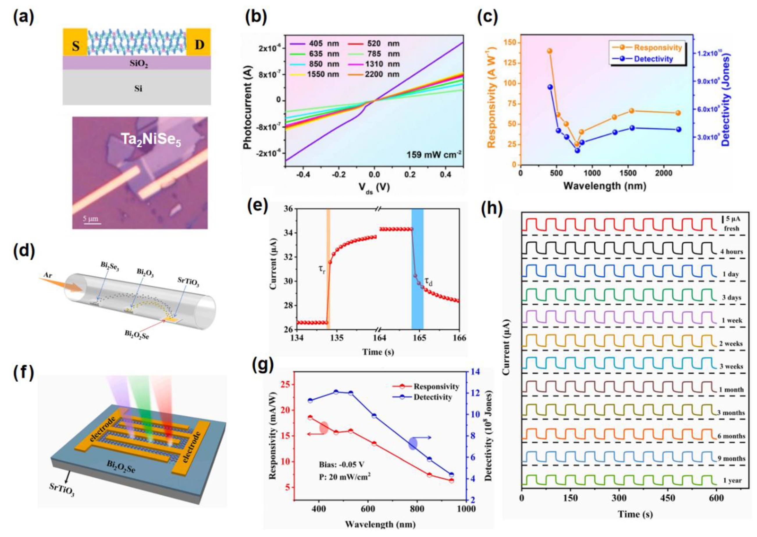
Figure 2.
(a) Structure of flexible Sn-Pb perovskite photodetector. (b) R of Sn-Pb photodetector as a function of wavelength. (c) Response speed curve [59]. Copyright 2024, Wiley. (d) Schematic device structure of the (BA)2(MA)Sn2I7 photodetector. (e) Photocurrent dependence on light wavelength measured at 1 V bias voltage [60]. Copyright 2023, OSA publishing. (f) SEM images of MAPbBr3 nanoplates. The inset in (f) shows an optical image of the as-prepared photodetector. (g) Responsivity and photocurrent of MAPbBr3 photodetector under infrared laser irradiation. (h) Normalized time-resolved photocurrent of MAPbBr3 photodetector under pulsed laser irradiation with frequency of 333 Hz. (i) A single normalized cycle in (k) [61]. Copyright 2023, Wiley. (j) Schematic diagram of the MAPbBr3/Ag photodetector. (k) Energy levels of the MAPbBr3 photodetector under different illumination conditions. (l) R of the MAPbBr3 photodetector at different wavelength [62]. Copyright 2022, OSA publishing.
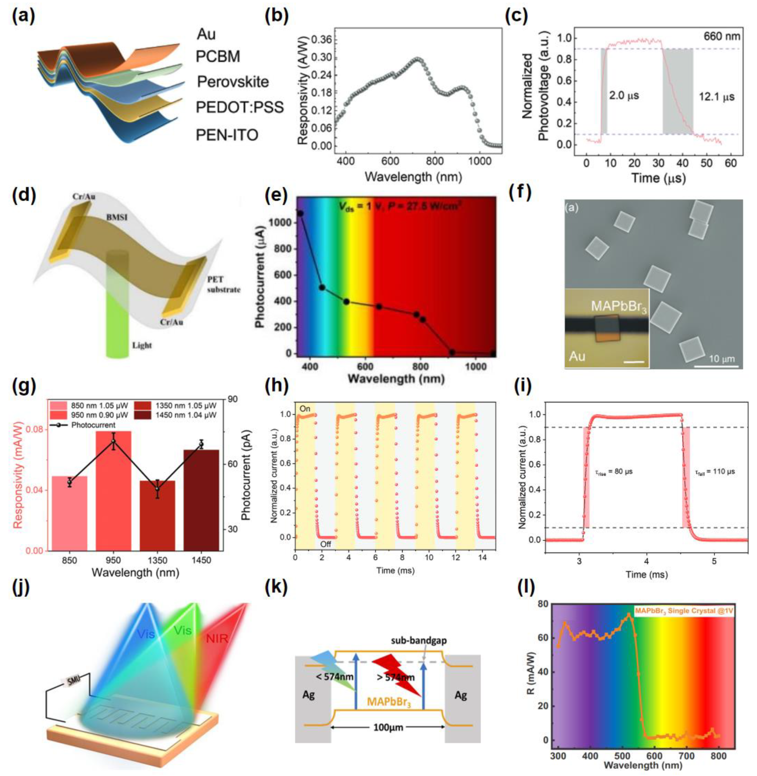
Figure 3.
(a) Structure of graphene photodetector. (b) Gate dependence of photocurrent under different illumination powers with excitation wavelengths at 1.3mm (c) Gate dependence of photocurrent under different illumination powers with excitation wavelengths at 3.2mm [65]. Copyright 2014, Macmillan. (d) Schematic diagram of the fully suspended rGO thin film photodetector. (e-f) Performance of a fully suspended rGO thin film photodetector from the UV to THz spectral region [66]. Copyright 2014, Elsevier. (g) Schematic diagram of the graphene photodetector device. (h) Responsivity and external quantum efficiency of the device. (i) Specific detectivity and noise equivalent power of the device [67]. Copyright 2023, Wiley. (j) Schematic diagram of the graphene photodetectors. (k) Normalized photocurrent profile acquired upon various excitation light wavelengths [68]. Copyright 2024, American Chemical Society.
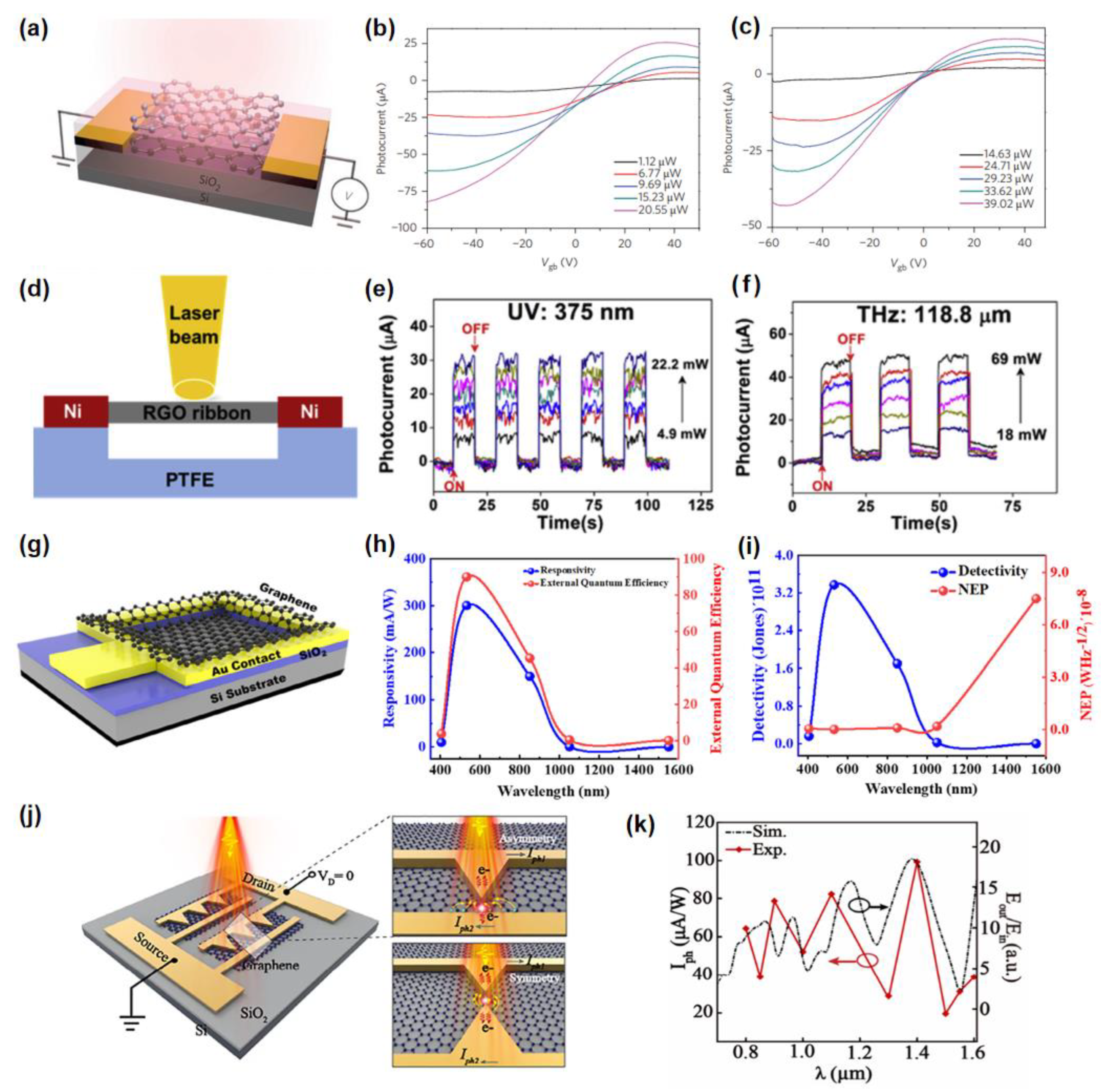
Figure 4.
(a) Typical SEM image of the Bi2Se3 nanowire device. (b) Spectral response of the device measured in the wavelength range of 380-980 nm. (c) Responsivity and detectivity of the device as a function of light intensity [70]. Copyright 2016, Royal Society of Chemistry. (d) Schematic illustration of the Sb2Te3 photodetector structure. (e) Wavelength dependency of current responsivity, at zero bias and room temperature, covering both visible to IR and THz spectral bands. (f) The top half panel demonstrates the band diagrams of the Sb2Te3 photodetector under illumination with limited positive (left) and negative (right) bias voltages, the bottom half panel demonstrates asymmetry in elastic scattering due to the wedge effect [71]. Copyright 2024, AIP Publishing. (g) Optical image of a TaIrTe4 device. (h) Broadband photoresponse of TaIrTe4 photodetector. Photoresponse of the TaIrTe4 device for different excitation wavelengths at 298 K [72]. Copyright 2018, American Chemical Society.
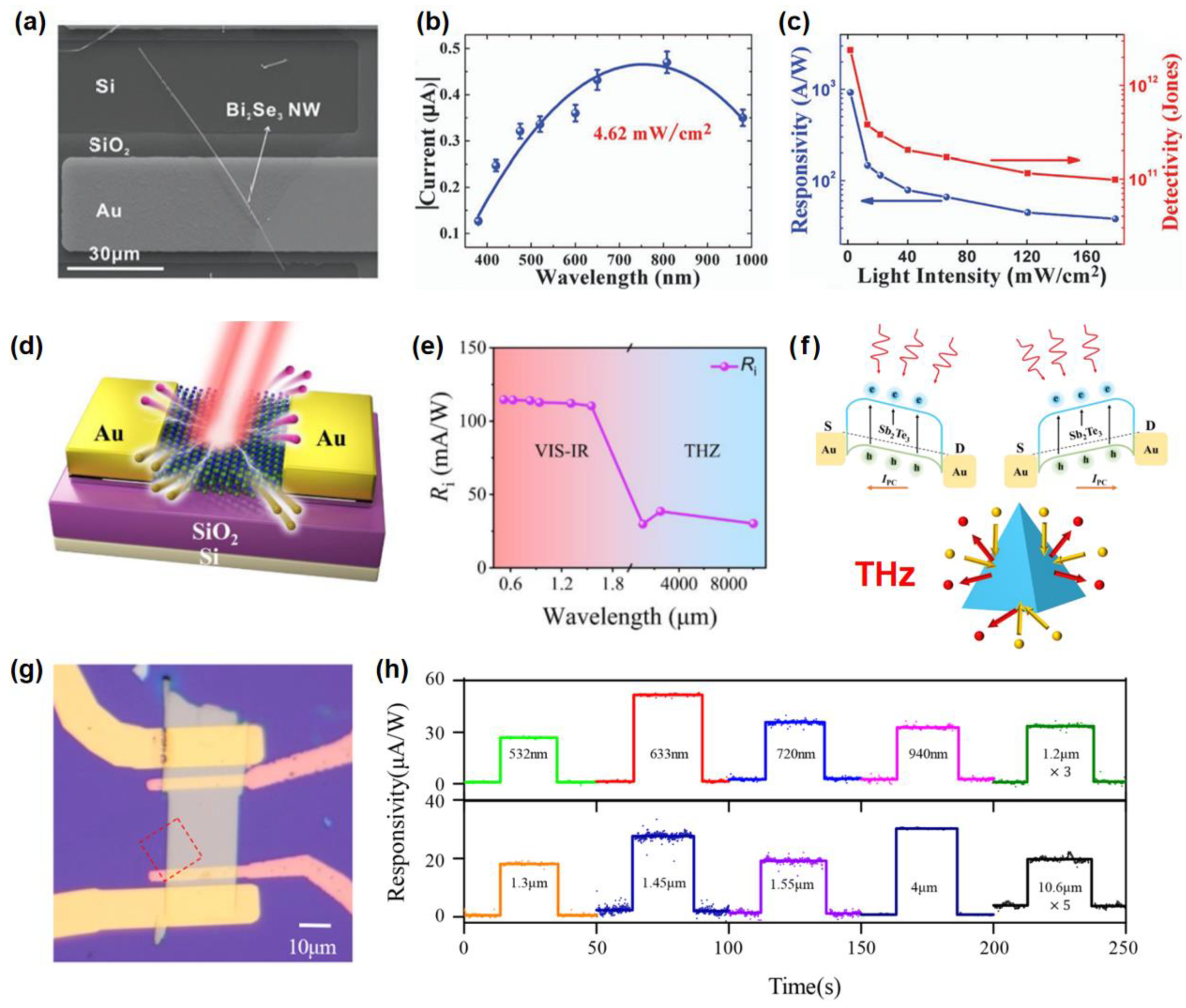
Figure 5.
(a) Structure of black phosphorus photodetector. (b) Responsivity and External quantum efficiency for different kinds of incident photons [75]. Copyright 2016, Wiley. (c) Structure of black phosphorus photodetector [76]. Copyright 2016, American Chemical Society. (d) Schematic diagram of black phosphorus photodetector. (e) Peak photocurrent for all wavelengths plotted as a function of incident flux. For all measurements a bias voltage of 200 mV and back gate of 0 V was used. (f) Photocurrent impulse response showing 65 ps rise time [78]. Copyright 2016, IOP.
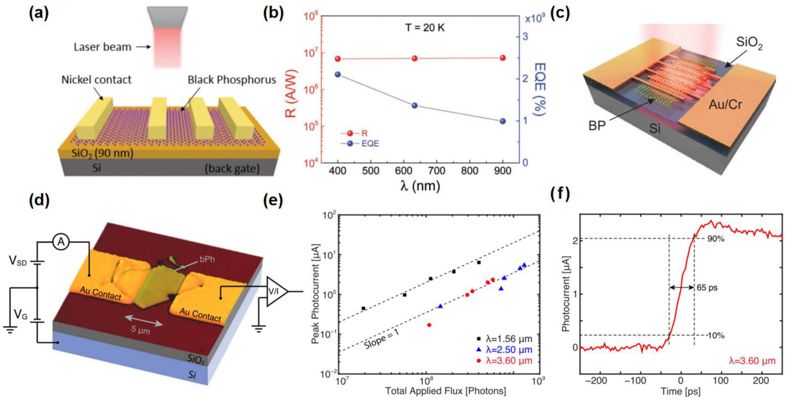
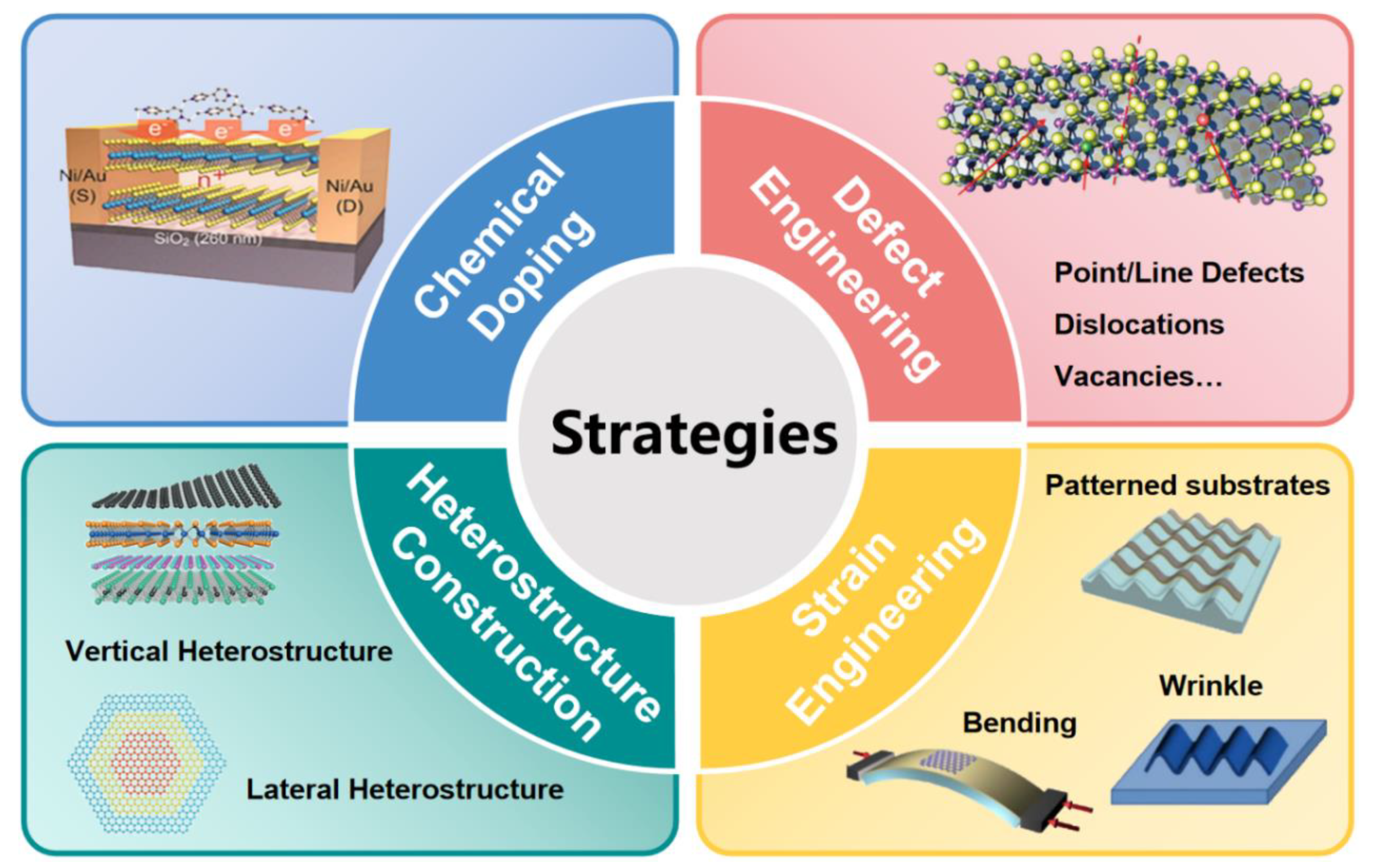
Figure 7.
(a) DFT calculation band structures for PbSe1-xTex. (b) The schematic diagram of PbSe1-xTex/MoSe2 device and the atomic structure models of PbSe1-xTex and MoSe2. (c) Responsivity and Detectivity of PbSe1-xTex/MoSe2 device from 405 to 5000 nm [95]. Copyright 2023, Wiley. (d) Responsivity and Detectivity of different types doped SnS photodetectors. (e) Schematic diagram and charge transfer mechanism for SnS/Mg. (f-g) I-t characteristics of SnS/Mg (2, 5, 7, 10, 12%) devices under visible and IR radiation [96]. Copyright 2024, American Chemical Society. (h) DFT calculated absorption spectrum of Mo16Se32, V1Mo15Se32, Mo15Se32 and V1Mo14Se32. (i) Responsivity of photodetectors based on MoSe2 with different V compositions as a function of excitation wavelength [98]. Copyright 2021, Elsevier. (j) Optical images of (GaN)1-x(ZnO)x photodetector. (k) Comparison of the responsivity with previous reports. (l) Comparison of the photoresponse time with previous reports [99]. Copyright 2024, Elsevier.
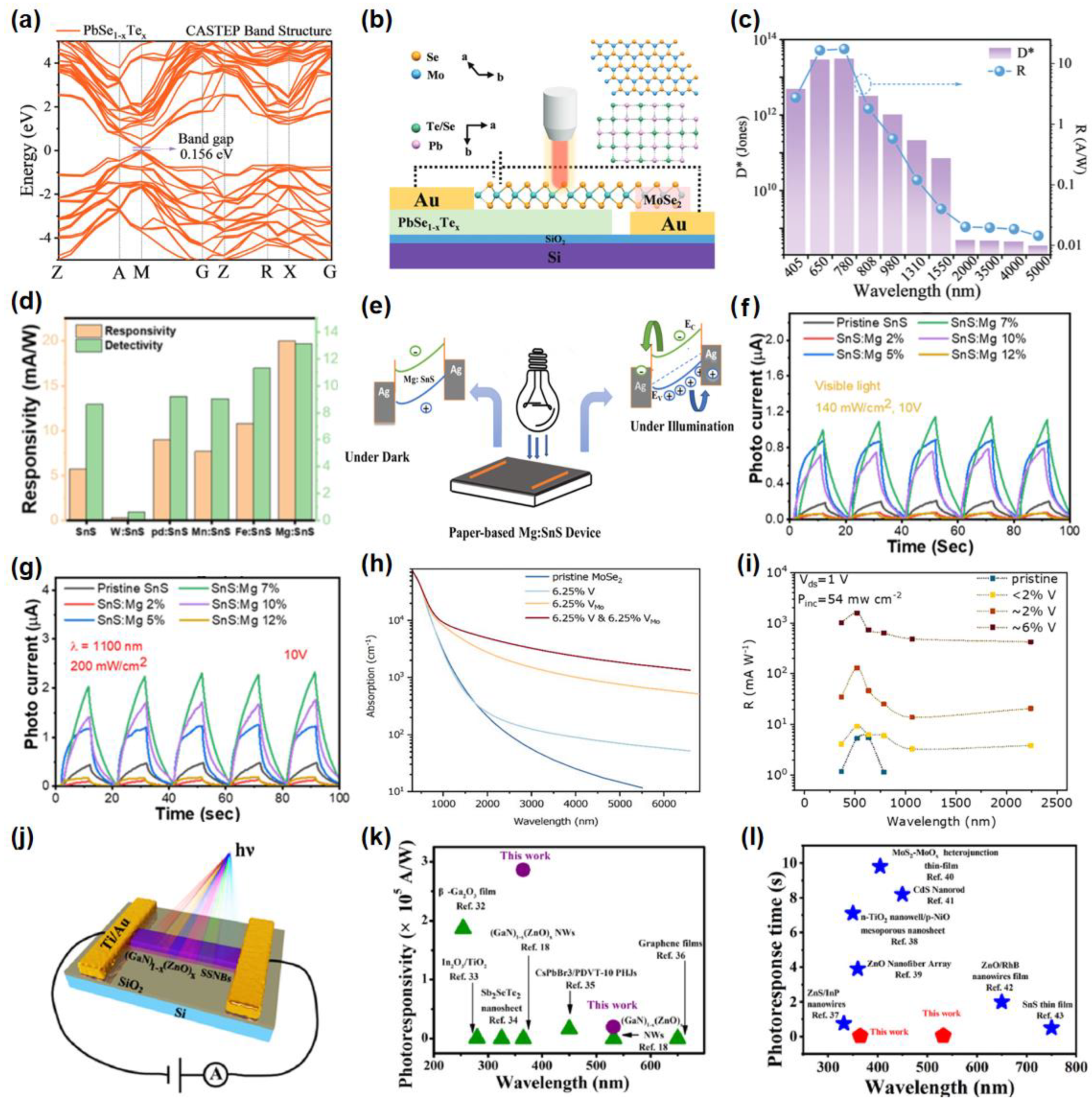
Figure 8.
(a) Schematic diagram of the WS2/AlOx/Ge photodetector. (b) Responsivity and EQE values of the photodetector as a function of light intensity. (c) Spectral photoresponse of the WS2/AlOx/Ge photodetectors and pure Ge photodetectors. Under light illumination of 1550 nm [100]. Copyright 2021, American Chemical Society. (d) Schematic diagram of the D-nMAG/Si photodetector. (e) The responsivity of D-nMAG/Si as a function of laser power density at 900 nm. (f) The responsivity of D-nMAG/Si as a function of laser power density at 4 μm [102]. Copyright 2022, Elsevier. (g) Schematic illustration of the Ni/MoS2 photodetector. (h) Energy band diagram of the MoS2 photodetector under negative voltage. (i) Responsivity and detectivity of the MoS2 device and the Ni/MoS2 device under 532 nm illumination at 5 V [103]. Copyright 2023, Duan et al.
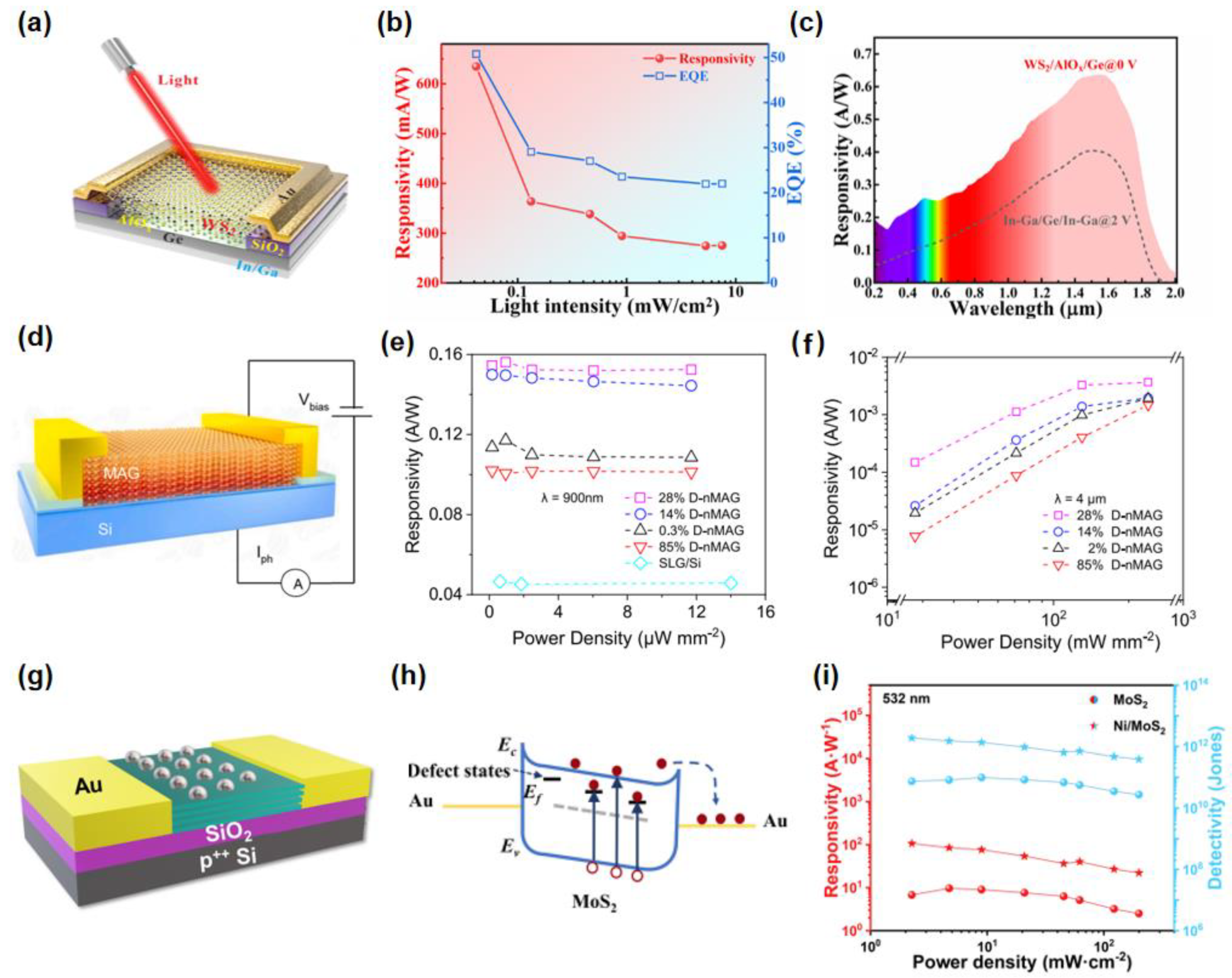
Figure 9.
(a) Schematic diagram of SnS2 QDs/MoS2 heterojunction. (b) Responsivity of the fabricated SnS2-QDs/MoS2 photodetector. (c) Band structure of SnS2-QDs and monolayer MoS2 after the formation of heterojunction [104]. Copyright 2022, American Chemical Society. (d) Schematic diagram of MoS2-on-ZnO heterojunction photodetectors. (e) Photocurrent curve of the MoS2-on-ZnO heterojunction photodetectors as a dependence of wavelength. (f) Schematic diagrams of band energy structure of MoS2-on-ZnO heterojunction under UV and visible light [105]. Copyright 2023, Springer. (g) Schematic diagram of the MoSe2/FePS3 photodetector. (h) Responsivity and EQE spectra of MoSe2/FePS3 photodetector measured at zero bias. (i) Straddling type-II configuration for multilayer MoSe2/FePS3 [106]. Copyright 2022, American Chemical Society. (j) Photodetector based on the quasi-vertical and vertical heterostructure of p-MoxRe1-xS2 /GaN. (k) Rise and fall times of high-resolution time-resolved photocurrent response of Vertical and Quasi-vertical photodetector. (l) The time-resolved photo response of Vertical p-MoxRe1-xS2/GaN heterostructure photodetector under different wavelength excitation at -5 V bias [107]. Copyright 2024, Wiley.
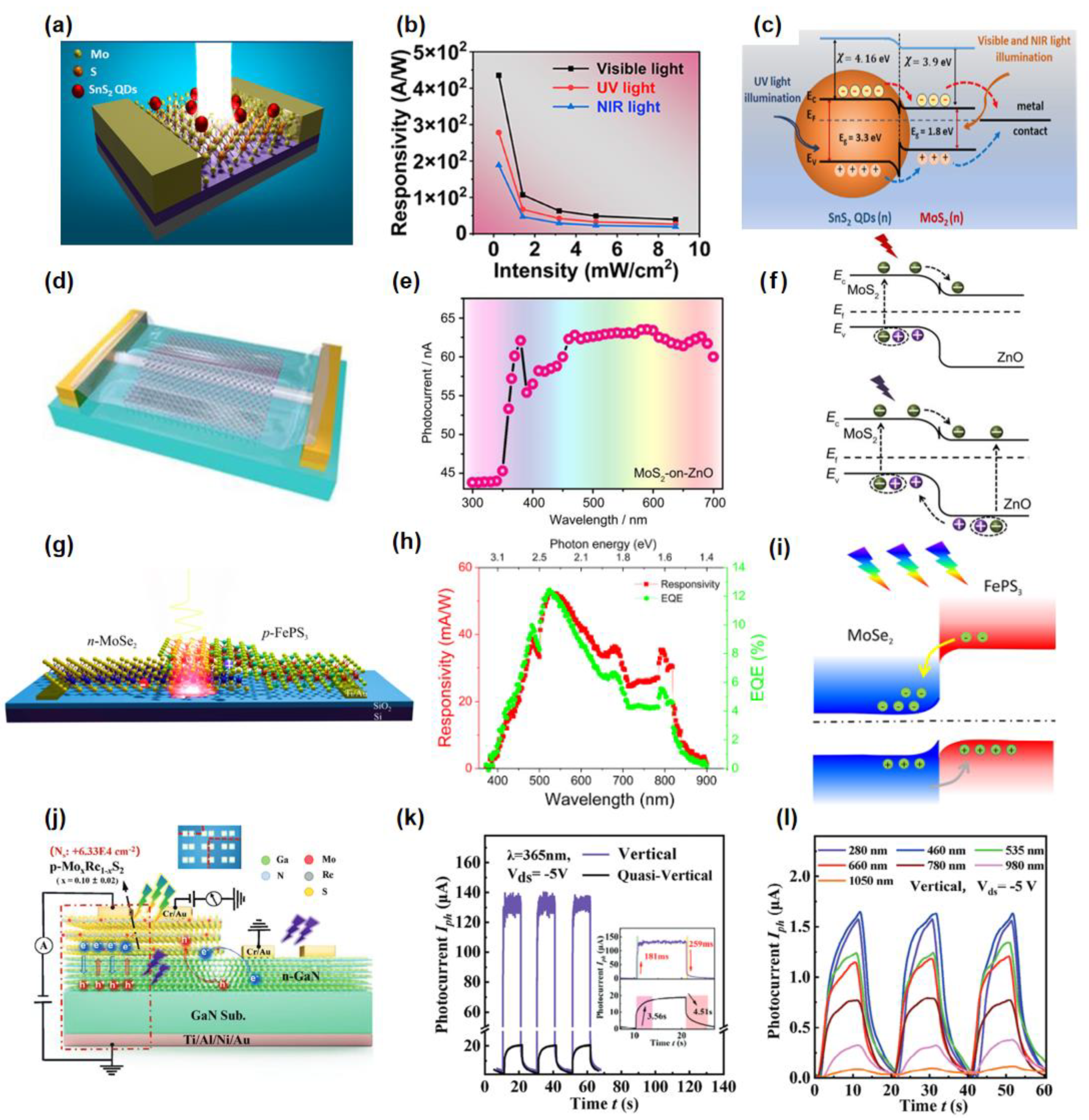
Figure 10.
(a) Optical image of a typical InSe/Te heterostructure device. (b) Energy band profiles of InSe and Te. (c) Photoswitching behavior of the device under different light wavelengths [108]. Copyright 2022, Wiley. (d) Schematic of MoS2/Sb2Se3 photodetector. (e) Spectral response of MoS2/Sb2Se3 photodetector. (f) Band-diagram of MoS2/Sb2Se3 photodetector [109]. Copyright 2023, American Chemical Society. (g) Schematic image of GeSe/SnS2 heterostructure photodetector. (h) The responsivity and detectivity curves irradiated under different wavelength from 255 to 1064 nm. (i) The band alignment of the GeSe/SnS2 heterostructure before and after contact [110]. Copyright 2024, AIP Publishing.
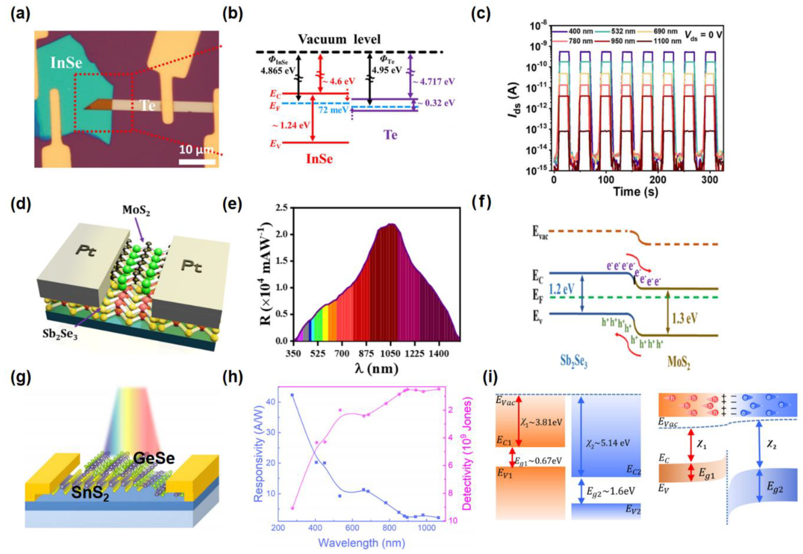
Figure 11.
(a) Schematics of strain-plasmonic coupled photodetector. (b) Schematic energy band diagram of the photodetection mechanism. (c) Time-dependent photo-response of pure MoS2 and Au NPs/MoS2 photodetectors under 660 nm, 680, 700, 720, and 740 nm light illumination [116]. Copyright 2022, Wiley. (d) Schematic of the Sb2Te3/MoS2 photodetector. (e) The measured photoresponsivity at different wavelengths (500 nm, 600 nm, 700 nm, 800 nm, and 900 nm). (f) The I–V characteristic of the Sb2Te3/MoS2 photodetector measured under varying strains [117]. Copyright 2023, MDPI.
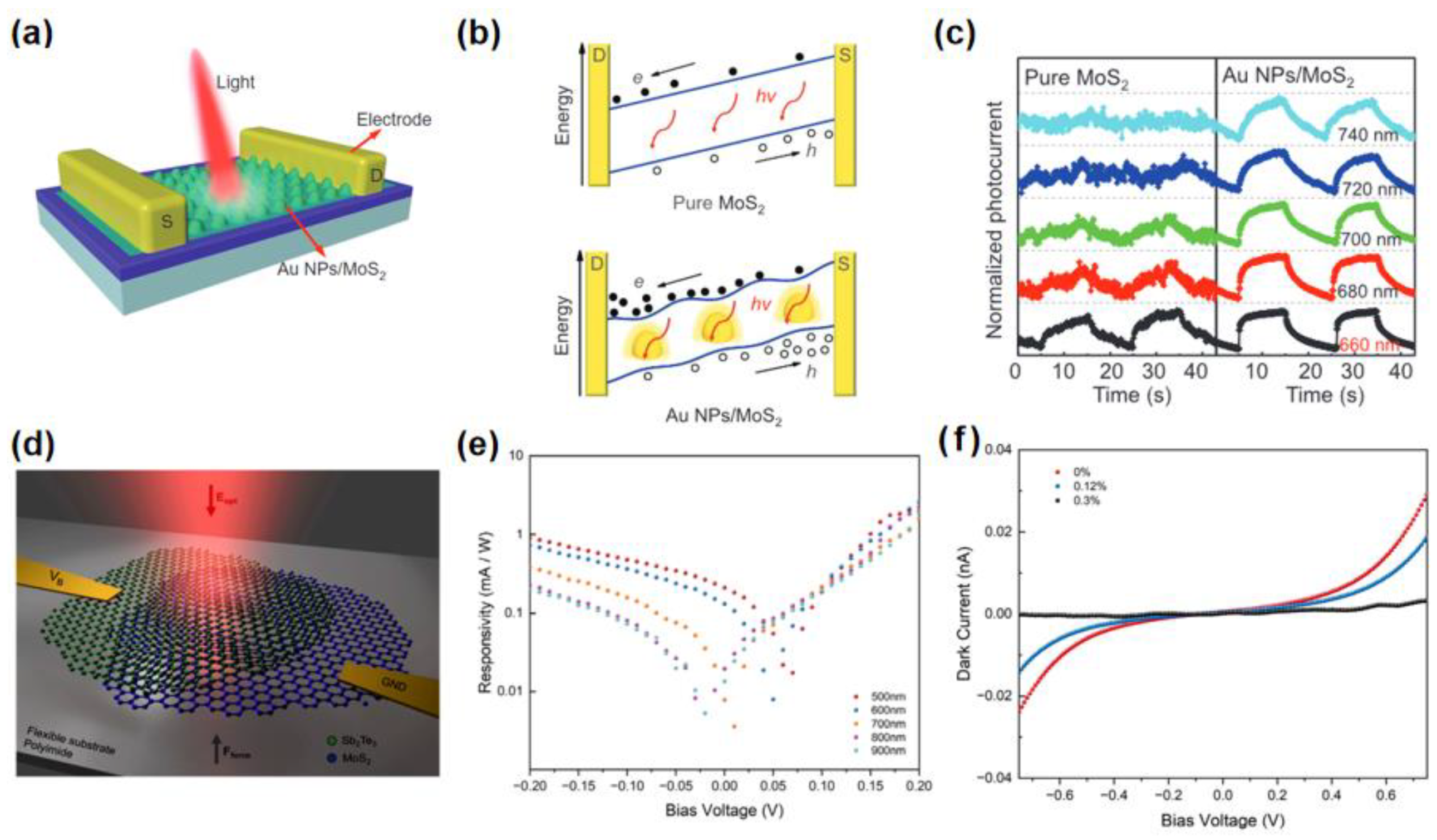
Figure 12.
(a) Schematic diagram of the heterostructure with gradient strain modulation. (b) SPCM of the vdWs heterostructure at zero bias voltage. (c) The mechanism explanation of the strain-enhanced optoelectronic performance of ZnO/WSe2 heterojunction [118]. Copyright 2022, Wiley. (d) Schematic diagram for photoelectric performance measurement under strain. (e) Time dependence of source-drain current of the photodetector during the light switching in armchair direction. (f) Time dependence of source-drain current of the photodetector during the light switching in zigzag direction [119]. Copyright 2019, Wiley.
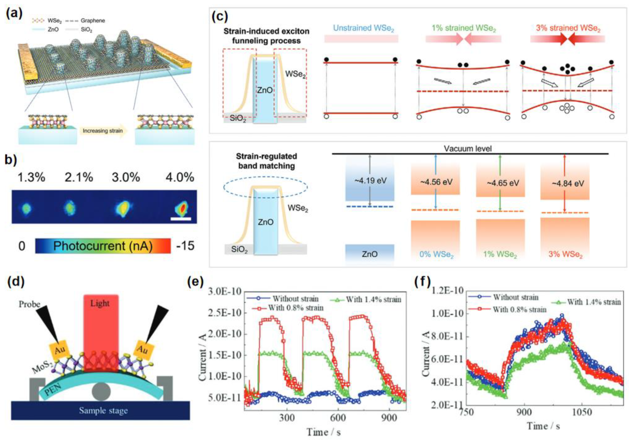

Table 1.
Comparison of various 2D materials broadband photodetectors.
| Device | Bias (V) | Range (nm) |
Responsivity (A/W) | Detectivity (109 Jones) |
EQE (%) | Ref. |
| Ta2NiSe5 nanosheets | 1 | 405-2200 | 138.9@405 nm | 8.4@405 nm | 4.3×10⁴ | [52] |
| Bi2O2Se thin film | -0.05 | 365-940 | 0.14@365 nm | 1.1@365 nm | - | [53] |
| Sn-Pb perovskite films | 0 | 350-1000 | 0.29@720 nm | 1.6@720 nm | - | [59] |
| CH3NH3PbBr3 crystal | 1 | 355-1560 | 0.23@520 nm | 143@520 nm | 55 | [62] |
| (BA)2(MA)Sn2I7 | 1 | 365-1064 | 28.4@365 nm | 23@365 nm | - | [60] |
| MAPbBr3 nanoplate | 2 | 850-1450 | 5.04@520 nm | 5370@520 nm | 1200 | [61] |
| Te nanosheets | 3 | 261-405 | 65000@261 nm | 0.37@261 nm | 2.2×10⁶ | [79] |
| Sb2Se3 thin film | 1 | 400-1200 | 3.37@1064 nm | 1.0@1064 nm | 393 | [80] |
| SnSe thin film | 0.8 | 400-1200 | 5.24@1064 nm | 4.2@1064 nm | 611 | [51] |
| SnTe nanosheets | 1 | 254-4650 | 71.11@254 nm | - | - | [81] |
| 4.17@4650 nm | ||||||
| GeTe nanofilm | 0.5 | 600-900 | 100@850 nm | 1000@850 nm | - | [82] |
| PdTe2 | 0.1 | 1-7.5 mm | 10@0.3 THz | - | [83] | |
| PtTe2 | -0.4 | 200-1650 | 0.406@980 nm | 3620@980 nm | 32.1 | [84] |
| PdPs | 1 | 254-1064 | 1180@532 nm | 440@532 nm | [85] | |
| Graphene | 1 | 375-118 μm | 1@532 nm | - | - | [66] |
| Graphene | 0 | 800-1600 | 0.025@1400 nm | - | - | [68] |
| InSiTe3 flakes | 11 | 365-1310 | 0.07@365 nm | 7.6@365 nm | - | [86] |
| Ga2In4S9 flakes | 5 | 330-900 | 112@360 nm | 225@360 nm | 2.2×10⁴ | [87] |
| TaIrTe4 | 0 | 532-10.6 μm | 0.02@10.6 μm | 0.18@10.6 μm | - | [72] |
| AgSbTe2 | 1 | 405-980 | 0.024@405 nm | 2@405 nm | - | [88] |
| Black phosphorus | -1 | 400-900 | 106@900 nm | - | 1×10⁹ | [75] |
| Black phosphorus | 0 | 2.5-3.7 μm | 0.047@2.7 μm | - | 2 | [77] |
Table 2.
The comparable table of working performance of some broadband photodetectors in recent years.
Table 2.
The comparable table of working performance of some broadband photodetectors in recent years.
| Device | Strategies | Range (nm) | Responsivity (A/W) | Enhancement | Ref. |
| PbSe0.5Te0.5 | Chemical Doping | 405-5000 | 17.5@780 nm | - | [95] |
| Mg-doped SnS | Chemical Doping | 400-1100 | 0.052@470 nm | 344% | [96] |
| MoSe2 with 6% V | Chemical Doping | 365-2240 | 9.7@520 nm | 625% | [98] |
| WS2/AlOx/Ge | Defect Engineering | 200-4600 | 0.63@1550 nm | 150% | [100] |
| D-nMAG | Defect Engineering | 900-4000 | 0.15@900 nm | 385% | [102] |
| CdSxSe1-x/Te | Heterostructure | 355-800 | 435@vis | 446% | [120] |
| MoSe2/FePS3 | Heterostructure | 350-900 | 0.052@522 nm | 144% | [106] |
| p-MoxRe1-xS2/ GaN | Heterostructure | 280-1050 | 888.69@365 nm | 352% | [107] |
| MoS2 | Strain Engineering | 660-740 | 660@418 nm | 400% | [116] |
| MoS2/Sb2Te3 | Strain Engineering | 500-900 | 0.001@600 nm | - | [117] |
Disclaimer/Publisher’s Note: The statements, opinions and data contained in all publications are solely those of the individual author(s) and contributor(s) and not of MDPI and/or the editor(s). MDPI and/or the editor(s) disclaim responsibility for any injury to people or property resulting from any ideas, methods, instructions or products referred to in the content. |
© 2025 by the authors. Licensee MDPI, Basel, Switzerland. This article is an open access article distributed under the terms and conditions of the Creative Commons Attribution (CC BY) license (http://creativecommons.org/licenses/by/4.0/).
Copyright: This open access article is published under a Creative Commons CC BY 4.0 license, which permit the free download, distribution, and reuse, provided that the author and preprint are cited in any reuse.


