1. Introduction
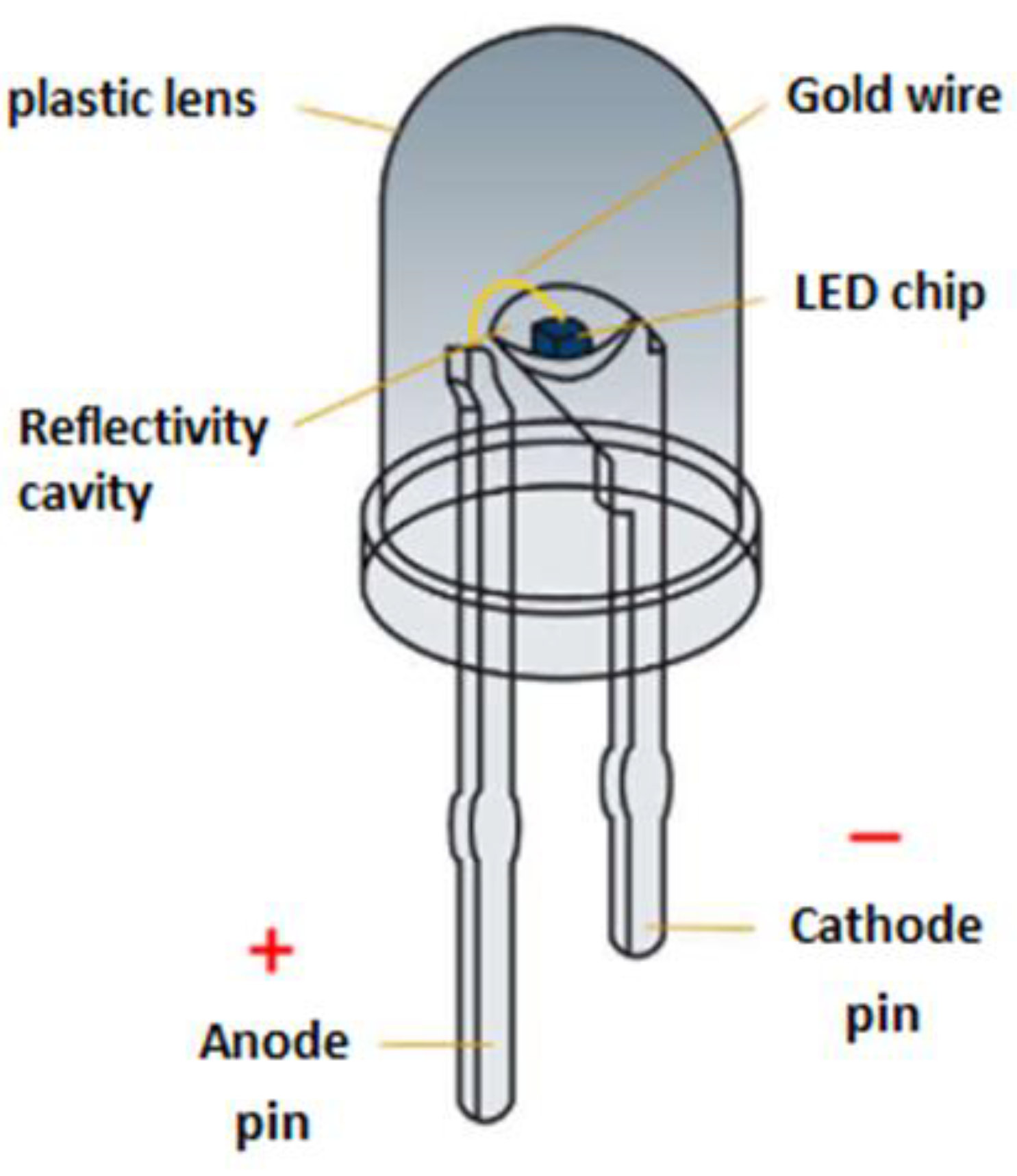
Light-Emitting Diodes (LEDs) are light sources based on a semiconducting LED chip and constructed of two pins (a cathode and an anode), a reflectivity cavity, a gold wiring, and a plastic lens that covers the device (
Figure 1). When voltage is applied, light is emitted, with the color dictated by the band gap of the semiconductor used in the device. LED lighting is energy-efficient and long-lasting, offering an environmentally responsible and sustainable technology. Its popularity stems from its ability to lower environmental impact while providing reliable performance. While LEDs have not yet been officially classified as electronic waste (e-waste), manufacturers proactively advise proper disposal. Although, currently, there is not a strong impetus to recycle LEDs, that might change shortly because of the following. First, consumers may replace LEDs sooner and before they seize to work due to rapid technological developments towards better performance at a lower cost. As a result, consumers may consider purchasing LED lights in the same way they do other electronic devices, replacing them well before their lifetime expires. This market trend is predicted to significantly increase LED production as well as LED waste in the environment. Second, LEDs are manufactured using a number of metals, including the more common iron and copper but also more valuable ones, such as aluminum, silver, gold, and more importantly gallium, arsenic, and indium among others. As the rates of production and use increase, critical metals like gallium, arsenic, and indium used in semiconductor manufacturing could be depleted within the next two decades. Based on the above reasoning, regulators and other government agencies are expected to introduce LED recycling programs to both reduce the environmental impact of LED waste and preserve the supply of critical metals essential for semiconductor manufacturing [1-5].
Current methods proposed for LED recycling include manual segregation, solvent dissolution, acid leaching, thermal treatment, or combinations thereof. Manual segregation typically involves mechanical processes such as prying, cutting, and cracking to separate the various components of the device [6, 7]. Dissolution employs solvents that dissolve some materials [8, 9], while leaching uses acids to extract valuable metals from the LED components [5, 10-13]. Thermal treatment, on the other hand, involves heating to high temperatures to facilitate decomposition followed by separation [7, 10, 14, 15]. Despite the effectiveness of these techniques, separating the LED components is often a labor-intensive and complex process that can jeopardize the benefits of recycling. The intricate structure of LEDs, which integrates multiple materials in compact designs, adds to the challenge of efficient disassembly and recovery. Given these challenges, researchers are actively searching for new, innovative and more sustainable methods for recycling LEDs.
Microwave treatment of e-waste has emerged as a fast and eco-friendly method, particularly suitable for recycling e-waste that contains both plastics and metals, including printed circuit boards, cell phones, CDs, and copper cable wires. Microwave irradiation selectively heats the metal due to its high conductivity, while the surrounding plastic undergoes pyrolysis, breaking down into gases, oils, and char. As the metal heats up during microwave treatment, it loosens up from the plastic matrix, enabling easy separation and recovery. Hence, this process has been explored for several applications including metal recovery from e-waste [16-25]. However, no studies have reported the use of microwave technology for processing LED e-waste to date [21, 22]. Herein, we demonstrate for the first time microwave-assisted recovery of critical and valuable metals from LED e-waste. The microwave process is remarkably fast, completing in under a minute. After microwave treatment, the LED components can be separated easily, reducing the need for intensive manual labor and minimizing the use of solvents or chemicals to dismantle the device components. Furthermore, the process is suited for batch processing, suggesting that it is appropriate for large-scale operations. Microwave-assisted separation holds significant promise in recycling LEDs, where speed and recovery efficiency are crucial. It has the potential to further streamline recycling processes, enhancing both effectiveness and sustainability.
2. Materials and Methods
All chemicals and solvents were purchased from Sigma-Aldrich. Experiments were conducted using a household microwave oven (frequency 2.45 GHz, wavelength
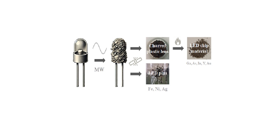
ca. 12 cm). Microwave treatment was carried out in a fume hood. LEDs of various colors-white, warm, red, pink, orange, yellow, green, and blue-were employed. The LEDs, each measuring 3 cm in size, were composed of three primary components: a plastic lens, an LED chip, and metallic pins (
Figure 1).
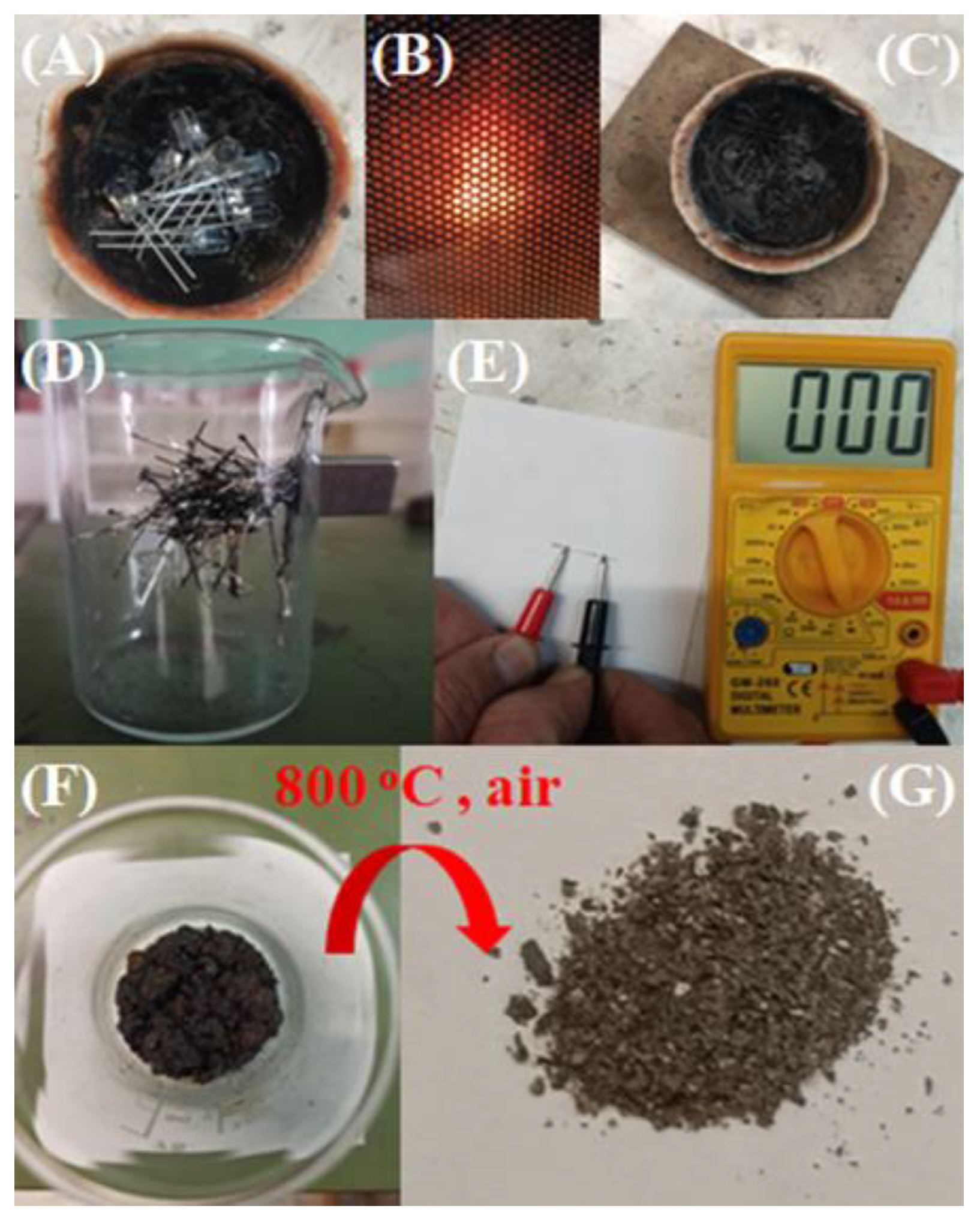
For the process, 10 to 20 LEDs were placed in a silica ceramic crucible and subjected to irradiation in a household microwave oven at 700 W under ambient air while rotating for 1 min. This microwave treatment resulted in the charring of the plastic lenses, which encapsulate the LED chip, while leaving the metallic pins intact. Subsequent mechanical separation of the components involved hand scraping to detach the charred plastic lenses followed by magnetic separation using a hand magnet to remove the metallic pins. The recovered metallic pins, referred to as PNLED, were both attracted by a magnet and they were conductive. The charred plastic residue was further treated by calcination in air at 800 °C for 1 hour, resulting in its complete removal from the chip, which we refer to as SMLED. Since the amount of SMLED is 0.1 mg per LED, approximately 400 LEDs were processed, in order to collect sufficient SMLED material. The complete process is illustrated in
Figure 2.
The structure and elemental composition of all samples were studied using complementary X-ray diffraction (XRD) and X-ray fluorescence (XRF) techniques. XRD patterns were obtained using a glass holder (for pins) or a background-free silicon wafer (for powders) with Cu Kα radiation (λ = 1.54 Å) from a Bruker Advance D8 diffractometer. Samples were scanned from 2-80° 2θ, in steps of 0.02° (2θ), at a rate of 0.2 s per step [
26]. Elemental analyses were carried out using a home-built Energy-Dispersive XRF spectrometer. Photons emitted from an annular
241Am source were used for sample excitation, while a Si(Li) crystal was used for the detection of fluorescent X-rays. Spectral analysis was carried out using the WinQxas software package developed by the International Atomic Energy Agency (IAEA, Vienna, Austria). Metallic pins were analyzed directly with no sample pretreatment. Quantitative analysis was performed using a custom fundamental parameters code developed specifically for the spectrometer. Powder samples were measured in the form of 1.25-cm-diameter pellets, prepared by mixing certain amount of finely ground sample with microcrystalline cellulose. Elemental quantification was based on calibration curves obtained for each analyte from sets of standard pellets prepared by mixing high-purity reagents with microcrystalline cellulose.
3. Results and Discussion
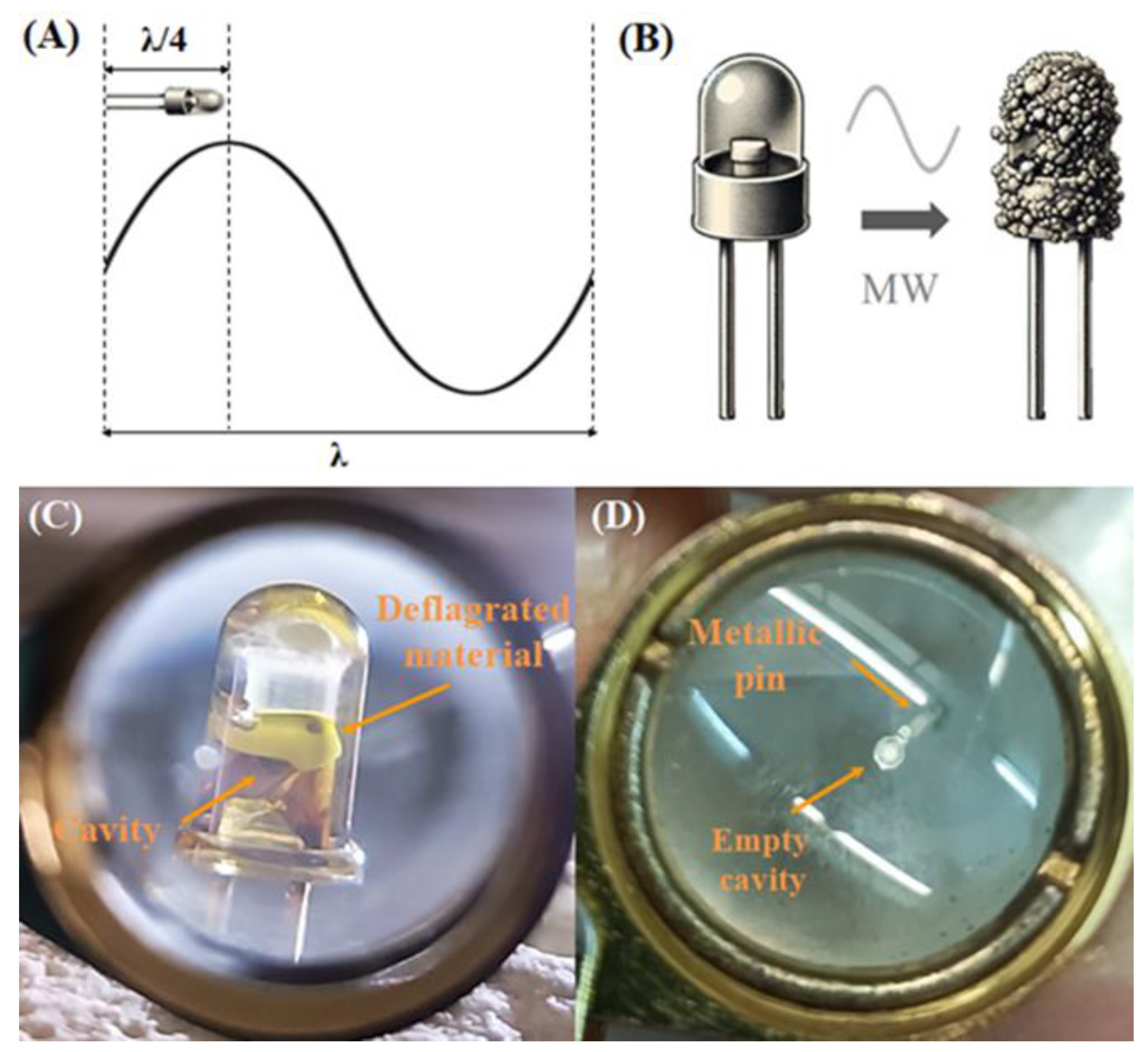
Due to their high conductivity the presence of the metallic pins in the LEDs, is key to the process. Since they are good conductors, they heat up rapidly in the microwave and the temperature increase initiates the recovery process. The size of the LED, being one-fourth of the microwave's standing wave wavelength, aligns with the peak of highest intensity in the wave (
Figure 3A). This resonance enhances the interaction between the microwaves and the LED, amplifying the heating and separation processes [23, 25]. This intense heating causes thermal expansion of the metallic pins (PNLED), weakening their bond with the surrounding plastic lens and, thus, facilitating their separation. The plastic lens deteriorates into a brittle char under the high temperatures generated by the microwaves (
Figure 3B), further softening the bonds and making the mechanical separation easier. During the initial stages of the microwave exposure, the LED chip deflagrates leaving the pin’s cavity empty (
Figure 3C, D). The brittle char encases the LED chip, allowing for easy separation from the metallic pin's reflective cavity. Finally, the char residue is calcined in air, exposing SMLED material. The resulting materials (PNLED and SMLED) are analyzed using complementary X-ray techniques-XRD for structural characterization and XRF to determine the elemental composition of the samples.
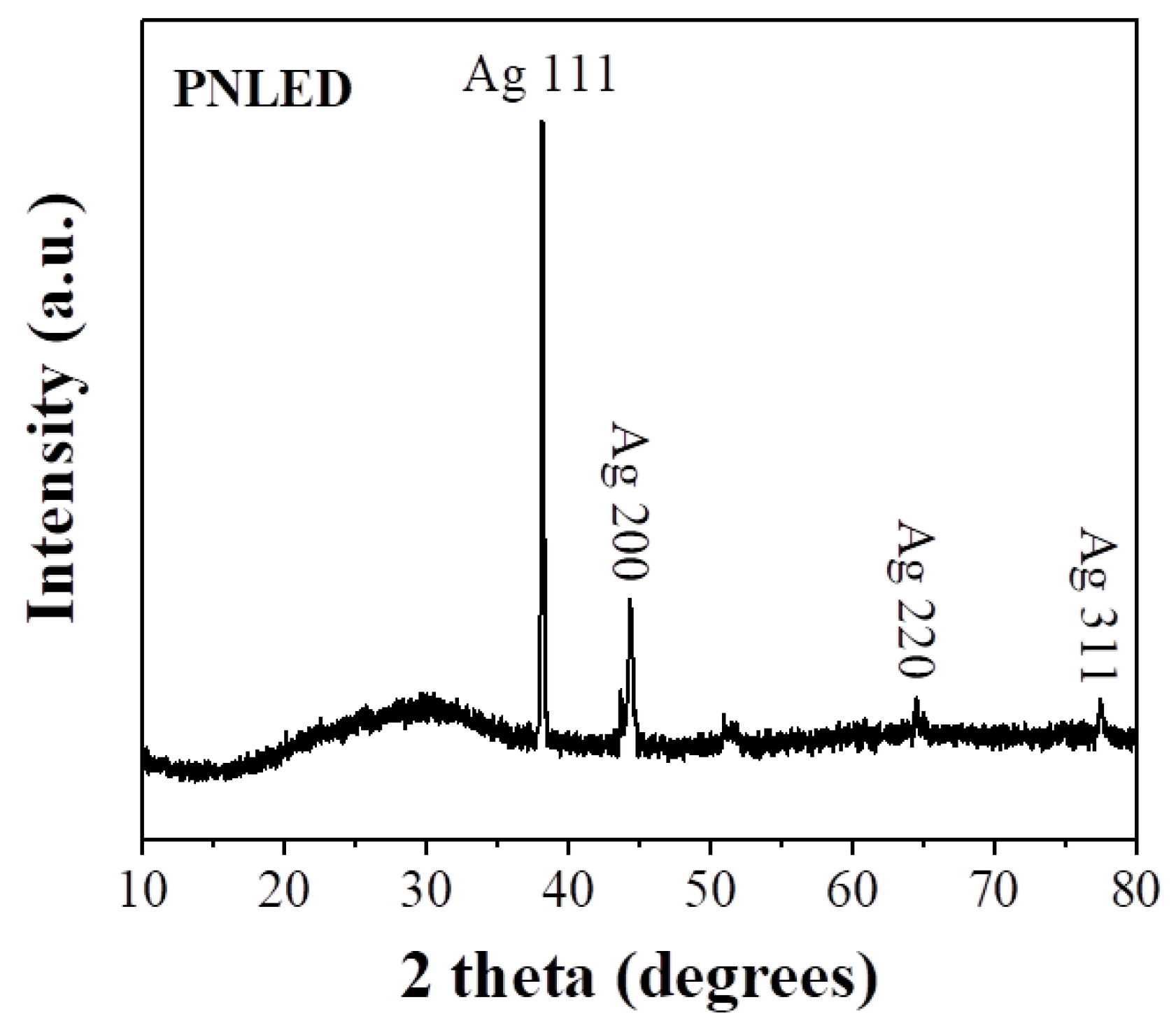
The XRD pattern of PNLED reveals characteristic reflections corresponding to the silver coating, as shown in
Figure 4. This confirms the presence of a silver layer on the surface of the pins. Complementary XRF analysis identifies additional elements (
Table 1), notably iron and nickel, which are absent in the XRD pattern. Among the latter, iron is present in a larger fraction and consistent with the observed magnetic properties of the metallic pins. The silver coating, on the other hand, accounts for the excellent conductivity of the pins. The detection of only silver in the XRD pattern is due to the nature of the coating. Silver, being a heavy polyelectronic element with a high atomic number, produces intense reflections in the XRD analysis, overshadowing signals from lighter elements like iron. Furthermore, the iron core is buried beneath the thin silver coating, reducing its contribution to the diffraction pattern. This combination of structural and compositional information illustrates the dual functionality of the metallic pins, with the iron core imparting magnetic behavior and the silver coating ensuring better conductivity. The magnetic properties of iron are not a critical factor in LED performance but may provide indirect benefits, such as electromagnetic compatibility in circuits and easy magnetic mounting and alignment of LED components. However, the primary reason for using iron in LEDs is its cost, as it is relatively inexpensive and readily available, making it a practical choice for manufacturers.
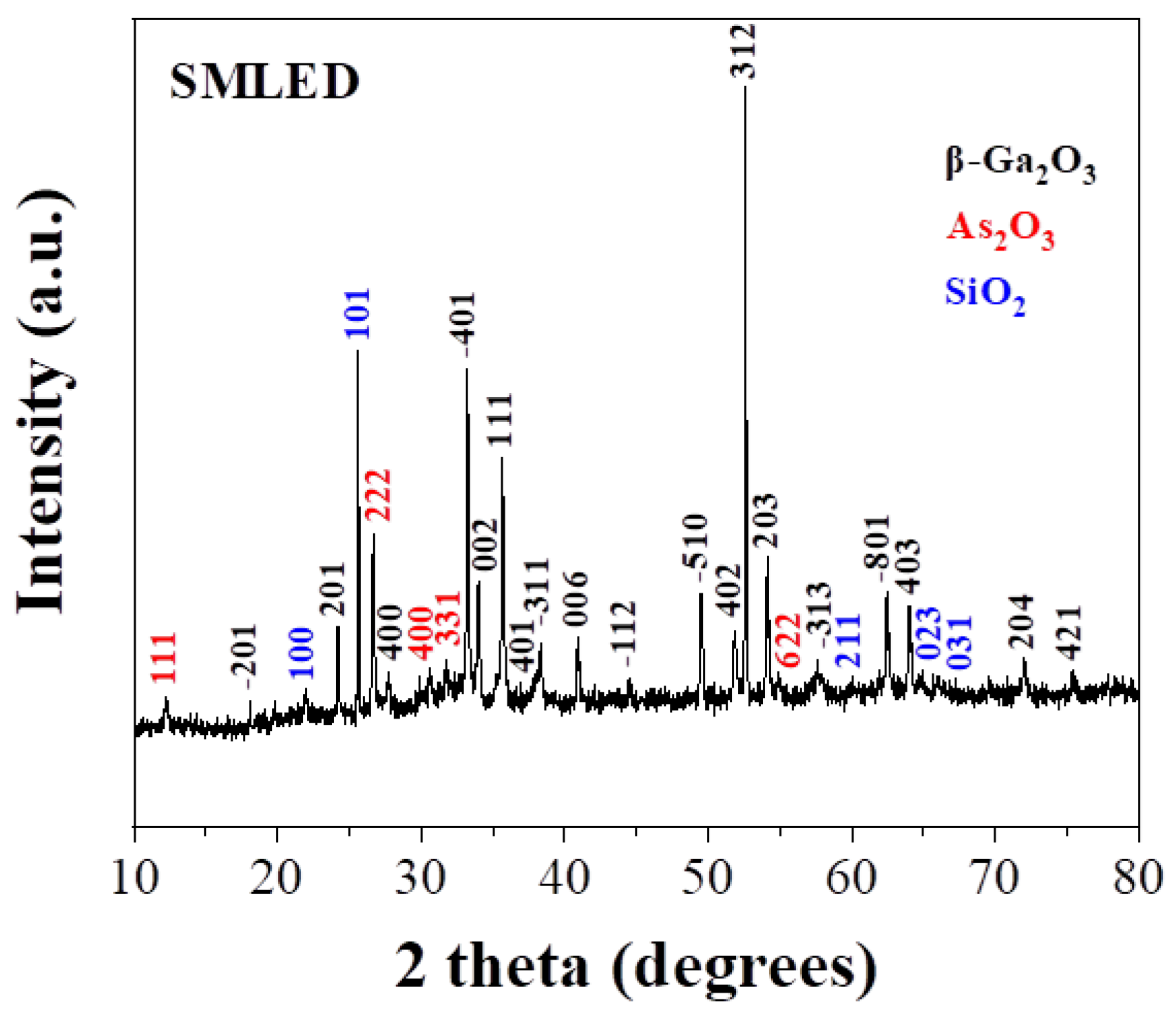
The XRD pattern of SMLED shown in
Figure 5 exhibits sharp reflections corresponding to β-Ga
2O
3 [27-29] and As
2O
3 [30, 31], confirming the presence of gallium and arsenic as expected for a GaAs based LED. Additionally, crystalline silica reflections are observed [
32]. These reflections are due to impurities introduced from the ceramic crucible during the microwave treatment. While the crucible is initially composed of amorphous silica, it undergoes localized crystallization near hot spots. These hot spots form because of microwave radiation interacting with metallic parts of the LED that come into contact with the crucible. The complete XRF composition of SMLED is detailed in
Table 1. In addition to Ga and As, elements including In, Au, Ag, Y, Ce, Sn, Pb, and Cu are present. Indium is used as dopant in GaAs. Yttrium and cerium come from the thin phosphor coating, which enhances light conversion efficiency. The presence of gold is due to the Au wires used for electrical connections, ensuring reliable conduction in the device, whereas the presence of Ag is due to silver coatings used as reflectors inside the LED to enhance light output by increasing reflectivity. Lead and tin come from the solder, which facilitates secure electrical contacts. Lastly, copper serves as the metallic substrate, contributing to effective thermal dissipation and cooling of the LED chip.
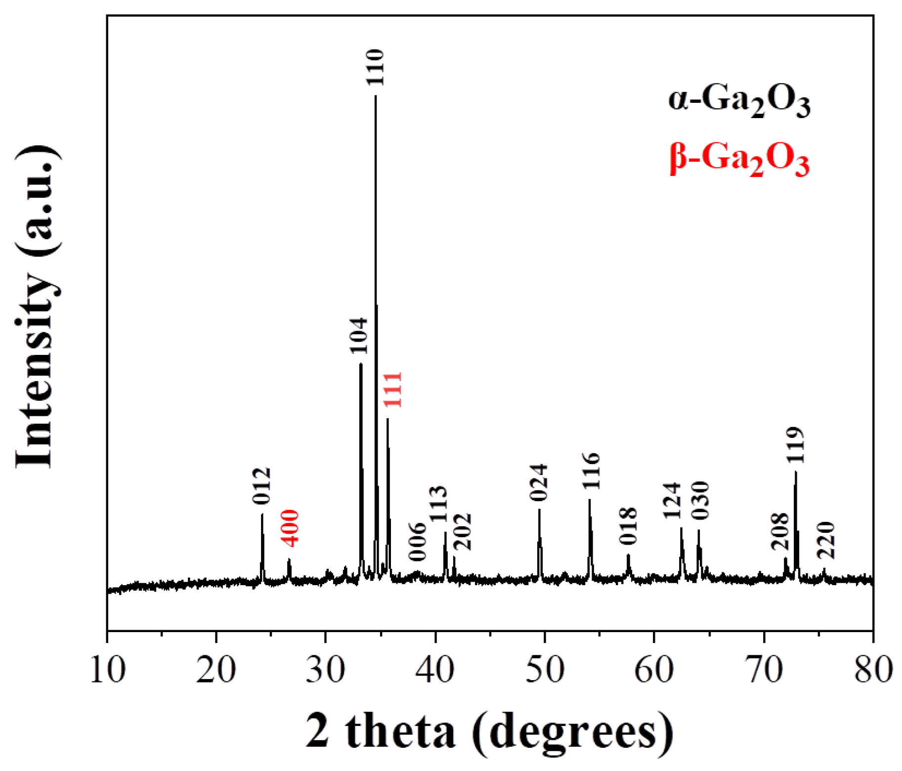
Based on the above results, SMLED has significant potential as a feedstock material for the extraction of critical metals essential to the electronic industry, including gallium, precious metals, and rare earths [4, 7, 10, 33-37], thus promoting resource recovery and reducing dependence on primary raw material sources. Separation and recovery of different metals from SMLED was explored using a two-step process. In the first step, acid treatment of SMLED with aqua regia (40 mg per 2 mL acid) at room temperature for 24 hours removes Cu, As, In, and Au with 75-100 % efficiency, and Ag and Sn with 40-60 % efficiency (
Table 1, SMLEDH material). Subsequent calcination of the remaining material at 800 °C in air enhances crystallinity, resulting in a solid with an XRD pattern similar to α-Ga
2O
3 [
38] (
Figure 6). Note that no As
2O
3 can be seen. Under acidic conditions, β-Ga
2O
3 converts to α-GaOOH after 24 hours of exposure through dissolution and recrystallization [
39]. Heat treatment at 800 °C dehydrates α-GaOOH, resulting in α-Ga
2O
3 [
40]. In the second step, the crystalline solid was treated with hot concentrated HCl (25 mg per 2 mL acid) at 100 °C for 2 hours. XRF analysis confirmed the complete leaching of rare earth elements Y and Ce, leaving behind a small quantity (approximately 1-1.5 mg) of a Ga-enriched solid (
Table 1, SMLEDHH material). The XRD pattern of the Ga-enriched solid, mounted on a background-free silicon wafer, displays a sharp and intense (110) reflection (not shown), which is the main peak of crystalline α-Ga
2O
3 [
41]. Typically, α-Ga
2O
3 (corundum-type) has a dense structure similar to α-Al
2O
3, which enhances its resistance to acid dissolution and facilitates gallium enrichment by removing any leachable species. Gallium is not leached out through this process, as chemically evidenced in the supernatant fractions by the addition of a gallium-precipitating agent, such as concentrated HF solution (GaF
3: K
sp ~ 10
-22). The addition of HF to the supernatant resulting from aqua regia treatment produces a precipitate composed of silver and tin, as indicated by XRF analysis, most likely due to the formation of insoluble Ag
2SnF
6, whereas the addition of HF to the supernatant after HCl treatment yields no precipitate. Overall, the stepwise application of aqua regia and hot concentrated HCl enables the efficient separation of different groups of critical elements for recovery or further processing [4, 7, 10, 33-37].
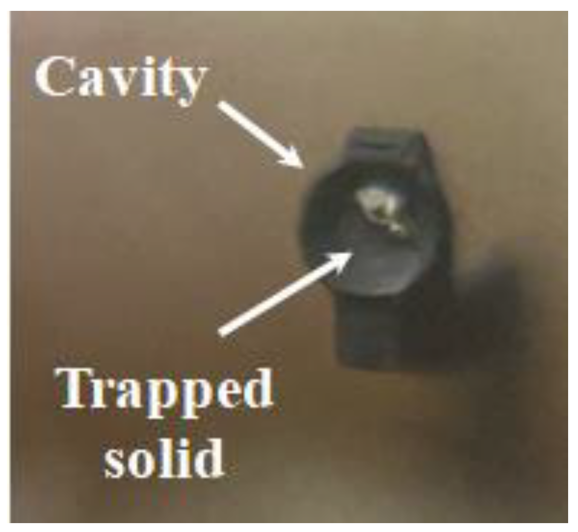
For comparison, conventional treatment by direct calcination of the LEDs at 800 °C in air for 1 h was also performed. This treatment can still separate the components, but it poses significant challenges of recovery because: (i) thermal heating reduces the recovery efficiency within the reflective cavity, as some of the LED chip materials deform, adhere, or become trapped, making the separation and extraction of the chip more difficult. Results obtained using a precision scale with five-digit accuracy showed that, in the case of microwave treatment, the LED chip is fully recovered, with a mass remarkably close to the expected value of 0.1 mg per LED, leaving the reflective cavity completely empty (
Figure 3D). In contrast, conventional heat treatment results in only partial recovery, with an efficiency of 45 % with some material remaining trapped in the cavity (
Figure 7).
Therefore, microwave treatment achieves 100 % recovery efficiency of the LED chip, while heat treatment reaches only 45 %; (ii) conventional heat treatment causes severe oxidation of the metallic pins into iron oxides, which compromises their structural integrity and renders them non-conductive (
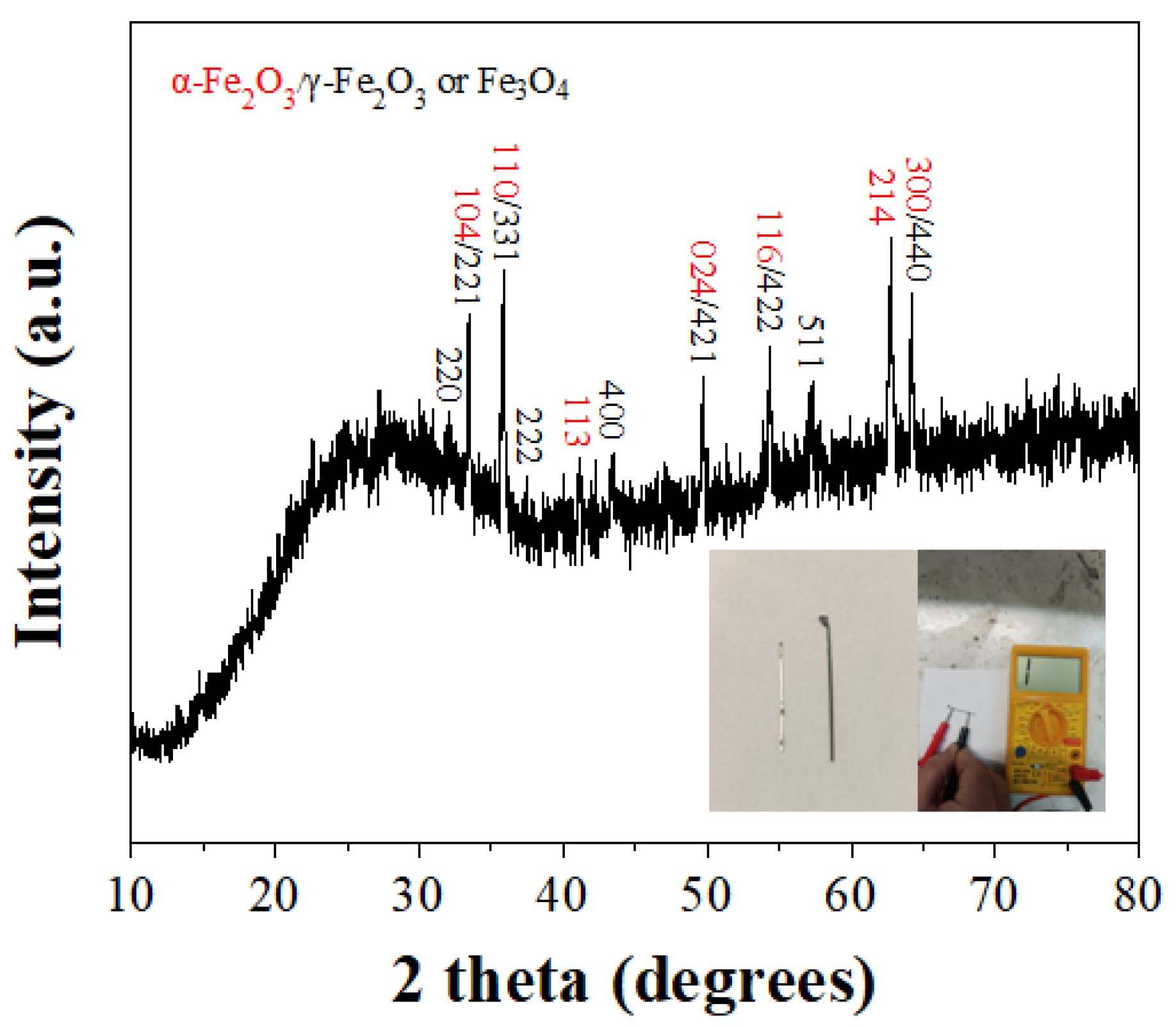
Figure 8). Silver can be detected in small amounts using XRF but not in the XRD in this case. When heated in air at 800°C, the iron core oxidizes, forming a thick iron oxide layer. This layer, along with the fact that silver is present in small amounts, can completely obscure the detection of silver by XRD. Thus, direct heating is less favorable as it does not fully recover the LED chip material and causes irreversible damage to the metallic pins, ultimately reducing the recovery efficiency of the LED components.
4. Conclusions
In this study, we introduce a microwave-assisted, efficient recycling method for Ga, As and other precious or critical elements present in LED devices. Microwave irradiation transforms the plastic lens of LED into a brittle char while simultaneously weakening the bond between the semiconducting chip and metallic pins (Fe, Ni, Ag). This process enables mechanical separation with minimal effort, reducing reliance on labor-intensive or chemically intensive methods. During the microwave processing the LED chip penetrates the plastic lens and becomes embedded in the charred residue. Further calcination of the charred residue produces a solid with all the materials used for the LED chip including critical elements (e.g., Ga, As, In, Y, Au). A two-step acid treatment, involving aqua regia followed by hot concentrated HCl, effectively leached away several of these metals, resulting in considerable gallium enrichment as shown by complementary analytical techniques. XRD verified the crystalline structure of the isolated materials, while XRF provided detailed information into the elemental composition. The analysis confirmed the successful recovery of key materials, validating the effectiveness of the proposed recycling approach. The microwave process is efficient and scalable, making it an attractive option for industrial recycling operations. Its ability to achieve rapid heating through resonance effects which facilitates component separation in just a minute offers a significant advantage over traditional methods. All in all, our study demonstrates that the microwave-assisted approach not only improves recycling efficiency but also represents a sustainable pathway for managing the growing challenge of LED e-waste.
Author Contributions
Conceptualization—AB.B.; data curation—A.B.B, C.P., N.C., E.P.G., D.P.G., C.E.S. and M.A.K.; formal analysis—A.B.B, C.P., N.C., E.P.G., D.P.G., C.E.S. and M.A.K..; investigation—A.B.B, C.P., N.C., methodology—A.B.B.; supervision—A.B.B., N.C., and M.A.K.; validation—A.B.B, C.P., N.C., E.P.G., D.P.G., C.E.S. and M.A.K.; writing, original draft—A.B.B, N.C., E.P.G., C.E.S. and M.A.K,.; writing, review and editing—A.B.B., N.C., and E.P.G. All authors have read and agreed to the published version of the manuscript.
Funding
We acknowledge support of this work by the project “Advanced Nanostructured Materials for Sustainable Growth: Green Energy Production/Storage, Energy Saving and Environmental Remediation” (TAEDR-0535821) which is implemented under the action “Flagship actions in interdisciplinary scientific fields with a special focus on the productive fabric” (ID 16618), Greece 2.0-National Recovery and Resilience Fund and funded by European Union NextGenerationEU. The research project is implemented in the framework of H.F.R.I. Call “Basic research Financing (Horizontal support of all Sciences)” under the National Recovery and Resilience Plan “Greece 2.0” funded by the European Union-NextGenerationEU (H.F.R.I. Project Number: 15949). This work made use of the Cornell Center for Materials Research (CCMR) shared instrumentation facility. The authors acknowledge support by the Center for Alkaline-Based Energy Solutions (CABES), part of the Energy Frontier Research Center (EFRC) program supported by the U.S. Department of Energy, under Grant DE-SC-0019445.
Data Availability Statement
The datasets generated for this study are available upon reasonable request from the corresponding authors.
Conflicts of Interest
The authors declare no conflicts of interest.
References
- Lim, S.-R.; Kang, D.; Ogunseitan, O.A.; Schoenung, J.M. Potential environmental impacts from the metals in incandescent, compact fluorescent lamp (CFL), and light-emitting diode (LED) bulbs. Environ. Sci. Technol. 2013, 47, 1040–1047. [Google Scholar] [PubMed]
- Rahman, S.M. M.; Pompidou, S.; Alix, T.; Laratte, B. A review of LED lamp recycling process from the 10 R strategy perspective. Sustain. Prod. Consum. 2021, 28, 1178–1191. [Google Scholar]
- Wehbie, M.; Semetey, V. Characterization of end-of-life LED lamps: evaluation of reuse, repair and recycling potential. Waste Manag. 2022, 141, 202–207. [Google Scholar]
- Mandal, S.; Bakaruddin, B.R. B.; Jeon, S.; Lee, Y.; Kim, K.-W. Assessment of the recycling potential of valuable metals by mapping the elemental composition in discarded light-emitting diodes (LEDs). J. Environ. Manag. 2023, 328, 116900. [Google Scholar]
- Illés, I.B.; Kékesi, T. The production of high-purity gallium from waste LEDs by combining sulfuric acid digestion, cation-exchange and electrowinning. J. Environ. Chem. Eng. 2023, 11, 110391. [Google Scholar]
- Ruiz-Mercado, G.J.; Gonzalez, M.A.; Smith, R.L.; Meyer, D.E. A conceptual chemical process for the recycling of Ce, Eu, and Y from LED flat panel displays. Resour. Conserv. Recycl. 2017, 126, 42–49. [Google Scholar]
- Cenci, M.P.; Dal Berto, F.C.; Castillo, B.W.; Veit, H.M. Precious and critical metals from wasted LED lamps: characterization and evaluation. Environ. Technol. 2022, 43, 1870–1881. [Google Scholar] [PubMed]
- Zhu, P.; Ma, Y.; Wang, Y.; Yang, Y.; Qian, G. Separation and recovery of materials from the waste light emitting diode (LED) modules by solvent method. J. Mater. Cycles Waste Manag. 2020, 22, 1184–1195. [Google Scholar]
- Zhan, L.; Wang, Z.; Zhang, Y.; Xu, Z. Recycling of metals (Ga, In, As and Ag) from waste light-emitting diodes in sub/supercritical ethanol. Resour. Conserv. Recycl. 2020, 155, 104695. [Google Scholar]
- Swain, B.; Mishra, C.; Kang, L.; Park, K.-S.; Lee, C.G.; Hong, H.S. Recycling process for recovery of gallium from GaN an e-waste of LED industry through ball milling, annealing and leaching. Environ. Res. 2015, 138, 401–408. [Google Scholar]
- Chen, W.-S.; Hsu, L.-L.; Wang, L.-P. Recycling the GaN waste from LED industry by pressurized leaching method. Metals 2018, 8, 861. [Google Scholar] [CrossRef]
- Annoni, R.; Lange, L.C.; Amaral, M.C. S.; Silva, A.M.; Assunção, M.C.; Franco, M.B.; de Souza, W. Light emitting diode waste: potential of metals concentration and acid reuse via the integration of leaching and membrane processes. J. Clean. Prod. 2020, 246, 119057. [Google Scholar]
- Rebello, R.Z.; Lima, M.T. W. D. C.; Yamane, L.H.; Siman, R.R. Characterization of end-of-life LED lamps for the recovery of precious metals and rare earth elements. Resour. Conserv. Recycl. 2020, 153, 104557. [Google Scholar]
- Zhan, L.; Xia, F.; Xia, Y.; Xie, B. Recycle gallium and arsenic from GaAs-based e-wastes via pyrolysis-vacuum metallurgy separation: theory and feasibility. ACS Sustain. Chem. Eng. 2018, 6, 1336–1342. [Google Scholar]
- Li, B.; Tao, R.; Wu, Y.; Zhang, W.; Liu, X.; Wang, W. Study on the pyrolysis characteristics and reaction mechanisms of WLED packaging materials. J. Anal. Appl. Pyrol. 2023, 170, 105935. [Google Scholar]
- Sun, J.; Wang, W.; Liu, Z.; Ma, C. Recycli,ng of waste printed circuit boards by microwave induced pyrolysis and featured mechanical processing. Ind. Eng. Chem. Res. 2011, 50, 11763–11769. [Google Scholar]
- Anis, S.; Lestari, S.E. Production of liquid oil from thermolysis of electrical and electronic wastes (e-waste) under microwave irradiation. J. Phys. Sci. 2018, 29, 53–62. [Google Scholar]
- Anis, S.; Prasetyo, E. Conversion of hand phone case waste into liquid fuels in a microwave reactor. IOP Conf. Ser.: Earth Environ. Sci. 2019, 258, 012011. [Google Scholar]
- Huang, Y.-F.; Pan, M.-W.; Lo, S.-L. Hydrometallurgical metal recovery from waste printed circuit boards pretreated by microwave pyrolysis. Resour. Conserv. Recycl. 2020, 163, 105090. [Google Scholar]
- Anis, S.; Qudus, N.; Kusumastuti, A. Treatment of electrical and electronic waste to reduce environmental issue. J. Adv. Res. Fluid Mech. Therm. Sci. 2020, 72, 148–156. [Google Scholar]
- Risco, Á.; Sucunza, D.; González-Egido, S. Chemical recovery of waste electrical and electronic equipment by microwave-assisted pyrolysis: a review. J. Anal. Appl. Pyrol. 2021, 159, 105323. [Google Scholar]
- Andooz, A.; Eqbalpour, M.; Kowsari, E.; Ramakrishna, S.; Cheshmeh, Z.A. A comprehensive review on pyrolysis of e-waste and its sustainability. J. Clean. Prod. 2022, 333, 130191. [Google Scholar]
- [23] Horikoshi, S.; Hachisuga, N.; Serpone, N. Recycling of e-waste power cables using microwave-induced pyrolysis-process characteristics and facile recovery of copper metal. RSC Adv. 2024, 14, 29955–29964. [Google Scholar]
- Bourlinos, A.B.; Spyrou, K.; Moschovas, D.; Avgeropoulos, A.; Salmas, C.; Karakassides, M.A. Fast microwave carbonization of aluminum-coated plastic wastes and perspectives: the examples of CDs and snack bags. Next Mater. 2025, 6, 100333. [Google Scholar]
- Bourlinos, A.B.; Chalmpes, N.; Giannelis, E.P.; Gournis, D.P.; Moschovas, D.; Avgeropoulos, A.; Salmas, C.; Karakassides, M.A. Total recycling of copper cable scrap and production of carbon using fast microwave technology. Micro submitted. 2025. [Google Scholar]
- Chalmpes, N.; Tantis, I.; Bakandritsos, A.; Bourlinos, A.B.; Karakassides, M.A.; Gournis, D. Rapid Carbon Formation from Spontaneous Reaction of Ferrocene and Liquid Bromine at Ambient Conditions. Nanomaterials 2020, 10, 1564. [Google Scholar] [CrossRef]
- Delgado, M.R.; Areán, C.O. Surface chemistry and pore structure of β-Ga2O3. Mater. Lett. 2003, 57, 2292–2297. [Google Scholar]
- Shi, F.; Qiao, H. Influence of hydrothermal reaction time on crystal qualities and photoluminescence properties of β-Ga2O3 nanorods. J. Mater. Sci.: Mater. Electron. 2020, 31, 20223–20231. [Google Scholar]
- Meitei, S.R.; Devi, L.S.; Singh, N.K. Nanocrystalline β-Ga2O3 thin film prepared by electron beam evaporation for enhanced photodetection. J. Phys. D: Appl. Phys. 2023, 56, 395104. [Google Scholar]
- Bioud, Y.A.; Boucherif, A.; Belarouci, A.; Paradis, E.; Drouin, D.; Arès, R. Chemical composition of nanoporous layer formed by electrochemical etching of p-type GaAs. Nanoscale Res. Lett. 2016, 11, 446. [Google Scholar]
- Verma, Y.; Rana, S.V. S. Hepatotoxic manifestations of arsenic trioxide loaded poly (lactide-coglycolide) nanoparticles in wistar rat. J. Anesth. Pain Med. 2024, 9, 1–9. [Google Scholar]
- El-Faramawy, N.; Gad, A.; Alazab, H.A.; Farouk, S. Thermoluminescence assessment of quartz veins emplaced in Talc-Schist Metamorphic Rocks. Egypt, J. Mater. Res. 2022, 37, 3784–3791. [Google Scholar]
- Chen, W.-T.; Tsai, L.-C.; Tsai, F.-C.; Shu, C.-M. Recovery of gallium and arsenic from gallium arsenide waste in the electronics industry. Clean-Soil Air Water 2012, 40, 531–537. [Google Scholar]
- de Oliveira, R.P.; Benvenuti, J.; Espinosa, D.C. R. A review of the current progress in recycling technologies for gallium and rare earth elements from light-emitting diodes. Renew. Sust. Energ. Rev. 2021, 145, 111090. [Google Scholar]
- Vinhal, J.T.; de Oliveira, R.P.; Coleti, J.L.; Espinosa, D.C. R. Characterization of end-of-life LEDs: mapping critical, valuable and hazardous elements in different devices. Waste Manag. 2022, 151, 113–122. [Google Scholar]
- Balinski, A.; Recksiek, V.; Stoll, M.; Christesen, C.; Stelter, M. Liberation and separation of valuable components from LED modules: presentation of two innovative approaches. Recycling 2022, 7, 26. [Google Scholar] [CrossRef]
- Illés, I.B.; Kékesi, T. A comprehensive aqueous processing of waste LED light bulbs to recover valuable metals and compounds. Sustain. Mater. Technol. 2023, 35, e00572. [Google Scholar]
- Lavalley, J.C.; Daturi, M.; Montouillout, V.; Clet, G.; Areán, C.O.; Delgado, M.R.; Sahibed-dine, A. Unexpected similarities between the surface chemistry of cubic and hexagonal gallia polymorphs. Phys. Chem. Chem. Phys. 2003, 5, 1301–1305. [Google Scholar]
- Chiang, J.-L.; Yadlapalli, B.K.; Chen, M.-I.; Wuu, D.-S. A review on gallium oxide materials from solution processes. Nanomaterials 2022, 12, 3601. [Google Scholar] [CrossRef]
- Sharma, A.; Varshney, M.; Saraswat, H.; Chaudhary, S.; Parkash, J.; Shin, H.-J.; Chae, K.-H.; Won, S.-O. Nano-structured phases of gallium oxide (GaOOH, α-Ga2O3, β-Ga2O3, γ-Ga2O3, δ-Ga2O3, and ε-Ga2O3): fabrication, structural, and electronic structure investigations. Int. Nano Lett. 2020, 10, 71–79. [Google Scholar]
- Zhang, Y.; Yan, J.; Li, Q.; Qu, C.; Zhang, L.; Xie, W. Optical and structural properties of Cu-doped β-Ga2O3 films. Mater. Sci. Eng. B 2011, 176, 846–849. [Google Scholar]
|
Disclaimer/Publisher’s Note: The statements, opinions and data contained in all publications are solely those of the individual author(s) and contributor(s) and not of MDPI and/or the editor(s). MDPI and/or the editor(s) disclaim responsibility for any injury to people or property resulting from any ideas, methods, instructions or products referred to in the content. |
© 2025 by the authors. Licensee MDPI, Basel, Switzerland. This article is an open access article distributed under the terms and conditions of the Creative Commons Attribution (CC BY) license (http://creativecommons.org/licenses/by/4.0/).