
Submitted:
08 April 2025
Posted:
09 April 2025
You are already at the latest version
Abstract
Transition metal dichalcogenide (TMDC)-based two-dimensional (2D) type-II van der Waals heterostructures exhibit remarkable potential in next-generation optoelectronics, valleytronics, and spintronics. Nevertheless, the inevitable Fermi level pinning (FLP) effect at metal/TMDC interfaces intrinsically leads to elevated Schottky barrier heights (SBHs) and consequent contact resistance degradation. In this work, we present a first-principles investigation on the interfacial physics of metal-contacted WSe₂/MoSe₂ heterostructures with four representative electrodes (Ag, Al, Au, Pt). All the metal-WSe2/MoSe2 contacts induce significant metal-induced gap states (MIGSs), which are responsible for FLP inside the WSe2/MoSe2 band gaps. Ag-MoSe2 contact has the minimum electron SBH of 0.31 eV, where the Pt-WSe2 exhibits a minimum hole SBH of 0.43 eV. Upon inserting a 2D metal-doped metallic mWSe/mMoSe layer between WSe2/MoSe2 layer and metal electrodes, the MIGSs arising from the penetration of metal wave functions into the semiconductor layers can be effectively suppressed, leading to practically negligible SBHs both for electron and hole, and even a vanishing SBH is obtained, suggesting a high carrier injection efficiency. The achieved quasi-Ohmic contact characteristics provide a universal design paradigm for high-performance TMDC-based devices requiring ultralow contact resistance.
Keywords:
WSe2/MoSe2 heterostructures
; Fermi level pinning
; Schottky barrier height
; buffer layer
; carrier injection efficiency
1. Introduction
Among various two-dimensional (2D) materials, transition metal dichalcogenides (TMDCs) are attracting tremendous interest due to their promising applications in electronics [1,2], valleytronics [3], optoelectronics [4,5]and spintronics [6]. Specifically, dangling bond free surfaces of 2D TMDCs enable the flexible construction of van der Waals (vdWs) heterostructures, providing opportunities for developing new devices with advanced functions. The observation of moiré superlattice exciton states in WSe2/WS2 vdWs heterostructures experimentally provides an attractive platform for controlling excited states of matter [7]. Tunneling field effect transistors based on 2D TMDCs heterostructures with subthreshold swing smaller than 60 mV dec−1 were demonstrated previously [8,9]. Intriguingly, selection of appropriate TMDCs layers allows type II heterostructures to be constructed, in which the ultrafast dynamics of charge transfer across the vdWs interface and the spatial segregation of photo-generated holes and electrons can be achieved. The electron transfer from WSe2 to MoS2 taken place within 470 fs with 99% charge transfer efficiency in MoS2/WSe2 p-n heterojunctions was reported [10]. Policht et al. observed an ultrafast interlayer electron transfer of up to 69 fs in WS2/MoS2 type II band alignment by using 2D electronic spectroscopy [11]. Similar sub-ps level charge transfer processes were also demonstrated in MoS2/MoTe2, MoSe2/MoS2 and WSe2/WS2 heterostructures [12,13]. However, the photoresponse times drop to the order of μs when made these heterojunctions into optoelectronic devices [14,15].
Inevitably, 2D TMDCs-based devices have contact interfaces with metal electrodes, and the quality of the electrical contacts becomes particularly important on their performances. 2D semiconductors generally exhibit unfavorable band edges due to the strong excitonic effect and quantum confinement [16], thus, for most commercially available metals (with the work function ranging from 3.5 eV to 5.7 eV) [17] the formation of low resistance ohmic contacts to mask the intrinsic exceptional properties of 2D TMDCs is still challenging to obtain [18]. The Schottky barrier height (SBH) at the metal-2D TMDCs interfaces, not simply depending on the difference between the work function of the metal and the conduction band minimum (CBM)/valence band maximum (VBM) of the TMDCs due to the complex Fermi level pinning (FLP), is a measure of the barrier to charge injection. A large SBH leads to high contact resistance at the metal-TMDCs interfaces, reducing the carrier injection efficiency [19,20]. Therefore, it is highly desirable to decrease SBH (a low resistance ohmic contact with vanishing SBH) to gain a high performance of a device.
A Schottky pinning factor S is normally introduced to describe the strength of the FLP, which is defined as the change in SBH (ΦSBH) with respect to the metal work function (WF), i.e., S=|dΦSBH/dWF| [17,21,22]. Not that S is the slope of ΦSBH versus WF, typical values reported are in the range of 0~1 [17,21,22,23], where a value close to 0 corresponds to a strong pinning interface, and a weakly interacting metal-TMDCs system is achieved for S close to 1, indicative of approaching the ideal Schottky-Mott limit. The FLP effects can be normally attributed to the interfacial effects [24], surface traps [25] and metal-induced gap states (MIGSs) [24,26,27]. Several works reported that the FLP can be weakened by inserting a buffer layer between the TMDCs and metal experimentally and theoretically, such as hexagonal boron nitride (h-BN) [28,29], molybdenum trioxide (MoOx, x<3) [30], ultrathin TiO2 [31], graphene [32,33], ZnO [34], monolayer (ML) NbS2 [25], VS2 [26], and so on. These results show that the introduction of buffer layers is an effective strategy to break the direct metal-TMDCs interaction and destroy the interface states, improving the contact properties.
Beyond their established advantages in ultrafast optoelectronics and emerging quantum information applications [35,36,37], WSe₂/MoSe₂ heterostructures present unique opportunities for fundamental interface engineering studies. Through density functional theory (DFT) simulations of four conventional metals (Ag, Al, Au, Pt) interfaced with monolayer WSe₂/MoSe₂ heterostructures, we reveal universal Schottky-type contacts with characteristic Fermi-level pinning. No ohmic contact is observed, MoSe2 forms an N-type Schottky contact with Ag and Al electrodes with electron SBH of 0.31 and 0.88 eV, and a P-type Schottky contact with Pt and Au electrodes with hole SBH of 0.42 and 0.76 eV, respectively. A similar trend is also observed in metal-WSe2 contacts, where the Pt-WSe2 exhibits a minimum hole SBH of 0.43 eV. Furthermore, we also demonstrated that inserting a 2D materials metallic layer (mMoSe/mWSe) between the metals and WSe2/MoSe2 layer indeed weakens the interaction at the contacting interfaces, which can effectively suppress the MIGSs, depinning the Fermi level, and thus reducing all the SBHs significantly.
2. Computational Methods
We use the Projector Augmented Wave (PAW) method and plane wave basis set implemented in the Vienna ab initio simulation package (VASP) code to optimize the geometries [23,24]. Using the Perdew Burke Ernzerhof (PBE) exchange correction function to modify the generalized gradient approximation (GGA) function [38]. To ensure accuracy, the plane-wave cutoff energy is set to 600 eV. The Brillouin zone are sampled with special k-points of 5×5×1 for optimizing supercell structures and 10×10×1 for densities of states (DOS) calculations. DOS calculations are implemented by using Gaussian drag method with a drag width of 0.02 eV [39,40]. The calculation is considered complete only when the energy difference between two consecutive steps is less than 10-6 eV and the force acting on each atom is less than 0.01 eV/Å.
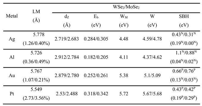
To accurately model metal electrode interfaces, six atomic layers of (111)-oriented Ag, Al, Au, and Pt slabs were employed based on converged surface properties established in prior studies [41,42]. The in-plane lattice constants of WSe2 and MoSe2 are a1=3.29 Å and a2=3.32 Å showed excellent agreement with experimental measurements [43,44]. A supercell with a lattice mismatch of less than 5% is needed to get stable structures of heterojunctions. Thus, the pristine metals/WSe2/MoSe2 supercells are constructed using a 2×2 expansion of Ag, Al, Au, and Pt (111) and a√3×√3 expansion of monolayer (ML) WSe2/MoSe2, resulting in lattice mismatches ranging from 0.21% to 3.56% as displayed in Tables 1. A vacuum layer exceeding 15 Å thickness was implemented along the z-direction to eliminate spurious interactions between periodic images.
3. Results and Discussion
Figure 1(a) and (b) illustrate the architecture of top-contact configurations where monolayer WSe₂/MoSe₂ interfaces with six-layer (111)-oriented metal slabs (Al, Ag, Au, Pt). The most stable configuration of the ML WSe2/MoSe2 on Ag and Au comes from the structure that the Se atoms are located at the center of a hexagon formed by six adjacent metal surface atoms, directly below the surface hollow site, where the W/Mo atoms are located above the center of a triangle formed by three neighboring metal atoms, as shown in Figure 1(a). Figure 1(b) displays the most stable configuration of Al- and Pt-WSe2/MoSe2 interfaces in which the W/Mo atoms sit above the center of the hexagons and Se atoms are above the centers of the triangles formed by metal atoms, respectively. Since the obtained results do not change appreciably beyond six layers of metal atoms [45], we restrict the simulation to this thickness. The equilibrium interfacial distances dz, defined as the difference between Se atoms and metal atoms along the z-direction (perpendicular to the interface) at the contact interfaces, varying from 2.488 to 2.912 Å, decreasing in the order of Al>Au>Ag>Pt (see Table 1). The binding energy of per interfacial Se atom is defined as
Eb = (EWSe2/MoSe2 + Emetal − E metal-WSe2/MoSe2)/NSe
Where Emetal, EWSe2/MoSe2, and Emetal-WSe2/MoSe2 are the relaxed energies for metal surface, WSe2/MoSe2, and the combined system per supercell, respectively, and NSe is the number of Se atoms at the interface of each supercell. Eb ranges from 0.182 eV (Al-WSe2) to 0.342 eV (Pt-MoSe2) as listed in Table 1, demonstrating the bonding strength trend. It can be found that Pt has a relatively strong adsorption (Eb =0.318/0.342 eV) and a small distance (dz=2.53/2.488 Å) with WSe2/MoSe2, showing a relatively strong bonding compared to those of other metals.
Before performing the metal-TMDCs systems investigation, we obtain the band structures of pure ML MoSe2 and WSe2 layers (see Figure S1 in the supporting information). The results show that ML WSe2/MoSe2 is a semiconductor with a band gap of 1.63/1.51 eV, which is consistent with previously reported values [46,47]. Figure 2 shows the projected band structures of metal-ML WSe2 combined systems where the band structures of metal-MoSe2 systems are presented in Figure 3. Both majority bands of ML WSe2 and MoSe2 are still identifiable when contacted with Ag, Al, Au and Pt surfaces. Although the conduction bands of MoSe2/WSe2 is reserved well when contacted with Pt, as shown in Figure 2(d) and Figure 3(d), the valence bands exhibit a slight hybridization, which are related to the d-orbital radius and occupied level of metals [47]. Actually, the band hybridization degree in different metal-MoSe2/WSe2 interfaces can be explained by the d-band model [48]. Pt has partially occupied d-orbitals leads to stronger bond with MoSe2/WSe2 than that of Ag and Au (full d-shells), which can mix with the band-edge d-orbitals of W and Mo, resulting in a better electron injection efficiency. This result is in good agreement with the binding energy calculation. Accordingly, Al is not a good choice for metal-MoSe2/WSe2 contact owing to the absence of d-orbitals [41,46], and a high resistance contact of Al-TMDCs has been verified experimentally [49].
After formation of the contacts, the Schottky barriers appear in the vertical direction, and thus vertical Schottky barriers height can be precisely determined by Φn= ECBM-EF (electrons) and Φp= EF-EVBM (holes), where ECBM, EVBM, and EF are the positions of the CBM, VBM, and Fermi level in the metal-MoSe2/WSe2 junctions, respectively. ΦSBH is crucial for the optical and electrical properties of MoSe2/WSe2 device. As shown in Figure 2(a) and (b), in Ag- and Al-WSe2 contacts, the Schottky barriers are N-type with electron SBHs of Φn= 0.43 and 1.1 eV, respectively. While in Au- and Pt-WSe2 contacts (see Figure 2(c) and (d)), the vertical Schottky barriers exhibit P-type, giving hole SBHs of Φp =0.66 eV and 0.43 eV. The extracted SBHs values for various metal-WSe2 combinations are listed in Table 1. Using a same approach, as displayed in Figure 3, SBHs for all of the metal-MoSe2 systems are calculated, and the extracted electron/hole SBHs as given in Table 1. Similarly, the Schottky barriers are N-type with Φn=0.31 and 0.88 eV in Ag- and Al-MoSe2, and are P-type with Φp = 0.76 eV and 0.42 eV in Au- and Pt-MoSe2, respectively. In these contacts, the large Φn of Al-MoSe2/WSe2 indicating a high resistance in the contact interfaces, which is consistent with the previous analysis. Actually, the contact polarity of Au-WSe2 has generally been reported to be ambipolar or P-type [50,51,52]. However, a predict N-type contact polarity could be realized with selenium vacancies [24]. A reported drop of P-type SBH from the transferred Au electrode (0.62 eV) to the evaporated Au electrode (0.19 eV) for WSe2 ML devices [51], indicating that a SBH value can be tuned by different fabricated approaches. Moreover, For Pt-MoSe2/WSe2 contact systems, the vertical hole SBHs (0.42/0.43 eV) is comparable with the one (0.55/0.34 eV) reported by other works [46,47].
Contact engineering is necessary to suppress the ΦSBH of the metal-TMDCs systems with the goal to achieve a low resistance Ohmic contact for 2D devices. An ultrathin buffer layer is a technologically viable approach to reduce the ΦSBH. It has been reported, for example, that a hBN buffer layer in Ni-MoS2 contact can decrease the SBH from 0.158 to 0.031 eV [53]. Also, a graphene buffer layer is effective in reducing the SBH from 0.3 to 0.19 eV in Ag-MoS2 configuration [54]. Moreover, thin oxides, such as Al2O3, have been used as buffer layer in Ti-MoS2, reducing the SBH from 0.18 to 0.13 eV [55]. Here, we report the metal-doped MoSe2/WSe2 (mMoSe/mWSe) acts as a buffer that can be sandwiched between metal electrodes and 2D MoSe2/WSe2 semiconductors (as illustrated in Figure 1(c)). It is important to stress that the configuration of metal atoms replacing Se atoms required less formation energy and is more stable than that of replacing Mo/W atoms, and a mMoS layer has been realized via a three-step plasma-deposition-annealing yttrium-doping process experimentally [56]. The metal-doping means to covert semiconducting MoSe2/WSe2 into metallic mMoSe/mWSe is theoretically predicted. Au-doping is taken as an example (see Figure S2), the band structure of AuMoSe/AuWSe with the VBM as well as the CBM coinciding in the Brillouin zone, confirming the zero bandgap metallic characteristic. Figure 4(a)-(d) show the projected band structures of metal-mWSe-WSe2 complexes. Obviously, after inserting an 2D mWSe layer into the contact interfaces, the barrier heights are reduced to 0.19, 0.04, 0.13 and 0.19 eV in the Ag-, Al-, Au- and Pt-mWSe-WSe2 contacts, respectively. While for metal-mMoSe-MoSe2 configurations, as shown in Figure 5(a)-(d), the corresponding vertical Schottky barriers are extracted to 0, 0.02, 0.03 and 0.29 eV, respectively. All the SBHs of electrons and holes are summarized in parentheses in Table 1. It is obvious that Φn is decreased significantly in the N-type contacts while Φp is relatively slight in the P-type contacts compared with those of without involving a buffer layer. Intriguingly, in contrast to the previous conclusion, the ultra-low Schottky barrier heights of Al-mMoSe/mWSe-MoSe2/WSe2 proves that Al becomes a good metal for low resistance contact after inserting the buffer layer. Furthermore, the transition from P-type contacts at Au-MoSe2/WSe2 interfaces to N-type contacts at Au-mMoSe/mWSe-MoSe2/WSe2 interfaces is observed. It is worth noting that a vanishing vertical N-type SBH in Ag-mMoSe-MoSe2 combined system indicates a low resistance Ohmic or quasi-Ohmic contact (Figure 5(a)), implying a high carrier injection efficiency.
Apparently, the extracted ΦSBH for various configurations are different from the predicted values by straightforward band alignment estimation, which are ascribed to the Fermi level pinning effect at the interfaces. To further quantify the strength of pinning behavior in different contacts, we plot the work function dependent Φn between semiconductor MoSe2/WSe2 and various metals systems, as shown in Figure 6. It is found that the SBHs of metal-WSe2 interfaces lie on a line of slope S=0.41, while those of metal-MoSe2 contacts lie on a line of slope S=0.33 (see Figure 6(a)), deviating from ideal Schottky-mott limit, indicating a strong pinning effect. Nevertheless, it is worth noting that these values are much larger than that of conventional semiconductor combines (GaAs (0.07) and Si (0.27)) [57]. For comparison, as exhibited in Figure 6(b), we also extract the value of S factors with mMoSe/mWSe buffer layers inserted between the metals and MoSe2/WSe2. A large pinning factor close to 1 (0.79 for metal-mMoSe-MoSe2 and 0.76 for metal-mWSe-WSe2) indicates a depinning Fermi level effect, which can be attributed to the reduction of the MIGS density in the contact stacks due to a weakened interaction between the metal and MoSe2/WSe2 layer. It is reported that an increased metal-TMDCs distance also can effectively suppress the MIGSs, and thus depinning Fermi level, reducing the SBHs [23].
To deeply understand the effect of conventional metals or mMoSe/mWSe layers on the ML MoSe2/WSe2 semiconductor, we calculate the partial density of states (PDOS) of pristine MoSe2/WSe2 and the contact systems. As shown in Figure 7(a)-(d), after contacted with metal faces, significant MIGSs are induced in the original band gap of WSe2 compared to that of the pristine WSe2 without contact (see Figure S3), which is consistent with previous studies [17,46]. It is observed that much more overlap interface states distributed in the pristine band gap for Pt contact compared with those of in other contacts (Figure 7(d)), indicating a strong hybridization in Pt-WSe2 combine, which is in agreement with the band structure hybridization degree. In contrast, as indicated in Figure 7(e)-(h), the corresponding metal-doped metallic mWSe in contact with ML WSe2 has negligible metal-induced gap states, leading to almost no additional Fermi-level pinning, which can be attributed to the native ideal vdWs interfaces between the mWSe and WSe2 layers. Moreover, similar contact nature trends are also obtained by comparing the PDOS in metal-MoSe2 and mMoSe-MoSe2 systems (see Figure S4 in the supporting information).
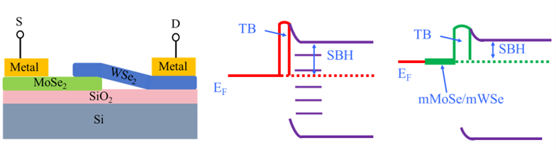
A prototype device (optoelectronic/electronic) based on MoSe2-WSe2 vdWs heterostructure consisting of a drain (D), a source (S) and a heterostructure channel is illustrated in Figure 8(a). dZ measured from optimized geometries (Table 1) and a notably high ΔV, defined as the potential energy above EF at the metal-WSe2/MoSe2 interfaces, is obtained (Figure S5), verifying the existence of tunneling barriers (TBs) [17,46]. In the light of TBs and Schottky barriers which are analyzed to evaluate the carrier injection efficiency of contacts, take N-type contact as an example, band diagrams for metal-WSe2/MoSe2 stacks and metal-interlayer-WSe2/MoSe2 stacks are shown in Figure 8(b) and (c), respectively. It is important to note that a narrow tunneling barrier and low Schottky barrier at metal-TMDCs interface can increase the carrier injection efficiency [17,18,46]. In the absence of buffer layer, a thin (even a vanishing) tunneling barrier is formed at the metal-WSe2/MoSe2 interface which is related to the band hybridization degree (Figure 8(b)). Although inserting a mMoSe/mWSe layer leads to a larger distance due to the nonbonding vdWs gap (~0.70 nm) between the mMoSe/mWSe and ML WSe2/MoSe2, resulting in a higher tunneling barrier, the weakened interaction at the interfaces can effectively suppress the formation of MIGSs (Figure 8(c)), thus reducing the SBHs.
4. Conclusions
The strategic modulation of Schottky barrier heights (SBHs) for both carrier polarities constitutes a critical advancement in developing high-efficiency two-dimensional optoelectronic devices. In this work, we have systematically investigated the contact interfaces between WSe2/MoSe2 heterojunction and a set of metals with a wide range of work functions (Ag, Al, Au, and Pt). Our calculation results show that the directly contacting WSe2/MoSe2 with various elemental metals leads to partial FLP due to the large density of MIGSs, and the electron/hole SBHs can be modulated effectively by varying metals (with the relatively large values ranging from 0.31 eV for Ag-MoSe2 contact to 1.11 eV for Al-WSe2 contact). A larger value of S close to 1 can be obtained by inserting a metal-doped mWSe/mMoSe layer as a metallic buffer between the metals and the 2D WSe2/MoSe2 semiconductor, suggesting a depinning Fermi level effect. In the presence of a buffer layer, both the polarities of Au-MoSe2 and Au-WSe2 contacts change from P-type to N-type, and all the SBHs can be reduced to a small even negligible value due to the suppression of MIGSs, implying a low resistance Ohmic contact. Our studies provide a theoretical reference for designing of high-performance 2D TMDCs devices.
Declaration of Competing Interest
The authors declare that they have no conflict of interest.
Supplementary Materials
The following supporting information can be downloaded at the website of this paper posted on Preprints.org.
Acknowledgments
This work was supported by the National Natural Science Foundation of China (No. 62264001), the Provincial Basic Research Program project of Guizhou (Nos. QKHJC-ZK [2022]YB009 and QKHJC-ZK[2022]YB014), and the High Level Innovation Talents Project of Guizhou Province (No. ZKHT-GCC[2023]007). The talent introduction start-up funds for scientific research project (GYU-KY-2025).
References
- An, J.; Zhao, X.; Zhang, Y.; Liu, M.; Yuan, J.; Sun, X.; Zhang, Z.; Wang, B.; Li, S.; Li, D. Perspectives of 2D materials for optoelectronic integration. Adv. Funct. Mater. 2022, 32, 2110119. [Google Scholar] [CrossRef]
- Chhowalla, M.; Jena, D.; Zhang, H. Two-dimensional semiconductors for transistors. Nat. Rev. Mater. 2016, 1, 1–15. [Google Scholar] [CrossRef]
- Long, X.; Deng, X.; Hu, F.; Xie, J.; Lv, B.; Liao, Y.; Wang, W. Tunable valley characteristics of WSe2 and WSe2/VSe2 heterostructure. Appl. Surf. Sci. 2023, 624, 157111. [Google Scholar] [CrossRef]
- Dhakal, K.P.; Roy, S.; Jang, H.; Chen, X.; Yun, W.; Kim, H.; Lee, J.; Kim, J. Local strain induced band gap modulation and photoluminescence enhancement of multilayer transition metal dichalcogenides. Chem. Mater. 2017, 29, 5124–5133. [Google Scholar] [CrossRef]
- Dai, T.; Liu, Y.; Fan, X.; Liu, X.; Xie, D.; Li, Y. Synthesis of few-layer 2H-MoSe2 thin films with wafer-level homogeneity for high-performance photodetector. Nanophotonics 2018, 7, 1959–1969. [Google Scholar] [CrossRef]
- Kurpas, M.; Junior, P.; Gmitra, M.; Fabian, J. Spin-orbit coupling in elemental two-dimensional materials. Phys. Rev. B. 2019, 100, 125422. [Google Scholar] [CrossRef]
- Jin, C.; Regan, E.C.; Yan, A.; Utama, M.; Wang, D.; Zhao, S.; Qin, Y.; Yang, S.; Zheng, Z.; Taniguchi, K.; Tongay, S.; Zettl, A.; Wang, F. Observation of moiré excitons in WSe2/WS2 heterostructure superlattices. Nature 2019, 567, 76–80. [Google Scholar] [CrossRef]
- Alam, K. Physical insight and performance metrics of monolayer MX2 heterojunction TFETs. Micro Nano Lett. 2020, 15, 81–85. [Google Scholar] [CrossRef]
- Choukroun, J.; Pala, M.; Fang, S.; Kaxiras, E.; Dollfus, P. High performance tunnel field effect transistors based on in-plane transition metal dichalcogenide heterojunctions. Nanotechnology 2018, 30, 025201. [Google Scholar] [CrossRef] [PubMed]
- Peng, B.; Yu, G.; Liu, X.; Liu, B.; Liang, X.; Bi, L.; Deng, L.; Sum, T.; Loh, K. Ultrafast charge transfer in MoS2/WSe2 p–n Heterojunction. 2D Mater. 2016, 3, 025020. [Google Scholar] [CrossRef]
- Policht, V.R.; Russo, M.; Liu, F.; Trovatallo, C.; Maiuri, M.; Bai, Y.; Zhu, X.; Conte, S.; Cerullo, G. Dissecting interlayer hole and electron transfer in transition metal dichalcogenide heterostructures via two-dimensional electronic spectroscopy. Nano Lett. 2021, 21, 4738–4743. [Google Scholar] [CrossRef]
- Conte, S.; Trovatello, C.; Gadermaier, C.; Gerullo, G. Ultrafast photophysics of 2D semiconductors and related heterostructures. Trends Chem. 2020, 2, 28–42. [Google Scholar] [CrossRef]
- Jin, C.; Ma, E.; Karni, O.; Regan, E.C.; Wang, F.; Heinz, T.F. Ultrafast dynamics in van der Waals heterostructures. Nat. Nanotechnol. 2018, 13, 994–1003. [Google Scholar] [CrossRef] [PubMed]
- Varghese, A.; Saha, D.; Thakar, K.; Jindal, V.; Ghosh, S.; Medhekar, N.; Ghosh, S.; Lodha, S. Near-direct bandgap WSe2/ReS2 type-II pn heterojunction for enhanced ultrafast photodetection and high-performance photovoltaics. Nano lett. 2020, 20, 1707–1717. [Google Scholar] [CrossRef] [PubMed]
- Ornelas, C.D.; Bowman, A.; Walmsley, T.S.; Wang, T.; Andrews, K.; Zhou, Z.; Xu, Y. Ultrafast photocurrent response and high detectivity in two-dimensional MoSe2-based heterojunctions. ACS Appl. Mater. Interfaces 2020, 12, 46476–46482. [Google Scholar] [CrossRef]
- Ugeda, M.M.; Bradley, A.J.; Shi, S.; Jornada, F.; Zhang, Y.; Qiu, D.Y.; Ruan, W.; Mo, S.; Hussain, Z.; Wang, F.; Louie, S.G.; Crommie, M.F. Giant bandgap renormalization and excitonic effects in a monolayer transition metal dichalcogenide semiconductor. Nat. Mater. 2014, 13, 1091–1095. [Google Scholar] [CrossRef]
- Ding, X.; Zhao, Y.; Xiao, H.; Qiao, L. Engineering Schottky-to-Ohmic contact transition for 2D metal–semiconductor junctions. Appl. Phys. Lett. 2021, 1, 18. [Google Scholar] [CrossRef]
- Y. Wang, M. Chhowalla, Making clean electrical contacts on 2D transition metal dichalcogenides. Nat. Rev. Phys. 2022, 4, 101–112.
- Ross, J.S.; Klement, P.; Jones, A.M.; Ghimire, N.J.; Yan, J.; Mandrus, D.G.; Taniguchi, T.; Watanabe, K.; Kitamura, K.; Yao, W.; Cobden, D.H.; Xu, X. Electrically tunable excitonic light-emitting diodes based on monolayer WSe2 p–n junctions. Nat. Nanotechnol. 2014, 9, 268–272. [Google Scholar] [CrossRef]
- Baugher, B.W.H.; Churchill, H.O.H.; Yang, Y.; Jarillo-Herrero, P. Optoelectronic devices based on electrically tunable p–n diodes in a monolayer dichalcogenide. Nat. Nanotechnol. 2014, 9, 262–267. [Google Scholar] [CrossRef]
- Liu, Y.; Guo, J.; Zhu, E.; Liao, L.; Lee, S.; Ding, M.; Shakir, I.; Gambin, V.; Huang, Y.; Duan, X. Approaching the Schottky–Mott limit in van der Waals metal–semiconductor junctions. Nature 2018, 557, 696–700. [Google Scholar] [CrossRef]
- Chen, J.; Zhang, Z.; Guo, Y.; Robertson, J. Metal contacts with Moire interfaces on WSe2 for ambipolar applications. Appl. Phys. Lett. 2022, 121, 051602. [Google Scholar] [CrossRef]
- Lizzit, D.; Khakbaz, P.; Driussi, F.; Pala, M.; Esseni, D. Ohmic behavior in metal contacts to n/p-type transition-metal dichalcogenides: Schottky versus tunneling barrier trade-off. ACS Appl. Nano Mater. 2023, 6, 5737–5746. [Google Scholar] [CrossRef]
- Noori, K.; Xuan, F.; Quek, S. Origin of contact polarity at metal-2D transition metal dichalcogenide interfaces. 2D Mater. Appl. 2022, 6, 73. [Google Scholar] [CrossRef]
- Wang, T.; Jin, H.; Li, J.; Wei, Y. Toward barrier free contact to MoSe2/WSe2 heterojunctions using two-dimensional metal electrodes. Nanotechnology 2018, 30, 015707. [Google Scholar] [CrossRef] [PubMed]
- Sotthewes, K.; Bremen, R.; Dollekamp, E.; Boulogne, T.; Nowakowski, K.; Kas, D.; Zandvliet, H.J.W.; Bampoulis, P. Universal Fermi-level pinning in transition-metal dichalcogenides. J. Phys. Chem. C. 2019, 123, 5411–5420. [Google Scholar] [CrossRef]
- Li, S.; Chen, J.; He, X.; Zheng, Y.; Yu, C.; Lu, H. Comparative study of the micro-mechanism of charge redistribution at metal-semiconductor and semimetal-semiconductor interfaces: Pt(Ni)-MoS2 and Bi-MoS2(WSe2) as the prototype. Appl. Surf. Sci. 2023, 623, 157036. [Google Scholar] [CrossRef]
- Pande, G.; Sian, J.; Chen, W.; Lee, C.; Sankar, R.; Chang, Y.; Chen, C.; Chang, W.; Chou, F.; Lin, M. Ultralow Schottky barriers in hexagonal boron nitride-encapsulated monolayer WSe2 tunnel field-effect transistors. ACS Appl. Mater. Interfaces 2020, 12, 18667–18673. [Google Scholar] [CrossRef]
- Farmanbar, M.; Brocks, G. Controlling the Schottky barrier at MoS2/metal contacts by inserting a BN monolayer. Phys. Rev. B. 2015, 91, 161304. [Google Scholar] [CrossRef]
- Chuang, S.; Battaglia, C.; Azcatl, A.; McDonnel, S.; Kang, J.; Yin, X.; Tosun, M.; Kapadia, R.; Fang, H.; Wallace, R.M.; Javey, A. MoS2 p-type transistors and diodes enabled by high work function MoOx contacts. Nano lett. 2014, 14, 1337–1342. [Google Scholar] [CrossRef]
- Kaushik, N.; Karmakar, D.; Nipane, A.; Karande, S.; Lodha, S. Interfacial n-doping using an ultrathin TiO2 layer for contact resistance reduction in MoS2. ACS Appl. Mater. Interfaces 2016, 8, 256–263. [Google Scholar] [CrossRef]
- Chanana, A.; Mahapatra, S. Prospects of zero Schottky barrier height in a graphene-inserted MoS2-metal interface. J. Appl. Phys. 2016, 119, 014303. [Google Scholar] [CrossRef]
- Chee, S.; Seo, D.; Kim, H.; Jang, H.; Lee, S.; Moon, S.; Lee, K.; Kim, S.; Choi, H.; Ham, M. Lowering the Schottky barrier height by graphene/Ag electrodes for high-mobility MoS2 field-effect transistors. Adv. Mater. 2019, 31, 1804422. [Google Scholar] [CrossRef] [PubMed]
- Jang, J.; Kim, Y.; Chee, S.; Kim, H.; Whang, D.; Kim, G.; Yun, S. Clean interface contact using a ZnO interlayer for low-contact-resistance MoS2 transistors. ACS Appl. Mater. Interfaces 2019, 12, 5031–5039. [Google Scholar] [CrossRef] [PubMed]
- Tran, K.; Moody, G.; Wu, F.; Lu, X.; Choi, J.; Kim, K.; Rai, A.; Sanchez, D. A.; Quan, J.; Singh, A.; Embley, J.; Zepeda, A.; Campbell, M.; Autry, T.; Taniguchi, T.; Watanabe, K.; Lu, N.; Banerjee, S. K.; Silverman, K. L.; Kim, S.; Tutuc, E.; Yang, L.; MacDonald, A.H.; Li, X. Evidence for moiré excitons in van der Waals heterostructures. Nature 2019, 567, 71–75. [Google Scholar] [CrossRef] [PubMed]
- Seyler, K.L.; Rivera, P.; Yu, H.; Wilson, N.P.; Ray, E.L.; Mandrus, D.G.; Yan, J.; Yao, W.; Xu, X. Signatures of moiré-trapped valley excitons in MoSe2/WSe2 heterobilayers. Nature 2019, 567, 66–70. [Google Scholar] [CrossRef]
- Jauregui, L.A.; Joe, A.Y.; Pistunova, K.; Wild, D.S.; Hign, A.A.; Zhou, Y.; Scuri, G.; Greve, K.; Sushko, A.; Yu, C.; Taniguchi, T.; Watanabe, K.; Needleman, D.J.; Lukin, M.D.; Park, H.; Kim, P. Electrical control of interlayer exciton dynamics in atomically thin heterostructures. Science 2019, 366, 870–875. [Google Scholar] [CrossRef] [PubMed]
- Perdew, J.P.; Burke, K.; Ernzerhof, M. Generalized gradient approximation made simple. Phys. Rev. Lett. 1996, 77, 3865. [Google Scholar] [CrossRef]
- Methfessel, M.; Paxton, A.T. High-precision sampling for Brillouin-zone integration in metals. Phys. Rev. B. 1989, 40, 3616. [Google Scholar] [CrossRef]
- Blöchl, P.E.; Jepsen, O.; Andersen, O.K. Improved tetrahedron method for Brillouin-zone integrations. Phys. Rev. B. 1994, 49, 16223. [Google Scholar] [CrossRef]
- Kang, J.; Liu, W.; Sarkar, D.; Jena, D.; Banerjee, K. Computational study of metal contacts to monolayer transition-metal dichalcogenide semiconductors. Phys. Rev. X. 2014, 4, 031005. [Google Scholar] [CrossRef]
- Kang, J.; Liu, W.; Banerjee, K. High-performance MoS2 transistors with low-resistance molybdenum contacts. Appl. Phys. Lett. 2014, 104, 233502. [Google Scholar] [CrossRef]
- Morales, J.; Santos, J.; Tirado, J.L. Electrochemical studies of lithium and sodium intercalation in MoSe2. Solid State Ionics 1996, 83, 57–64. [Google Scholar] [CrossRef]
- Al-Hilli, A.A.; Evans, B.L. The preparation and properties of transition metal dichalcogenide single crystals. J. Cryst. Growth 1972, 15, 93–101. [Google Scholar] [CrossRef]
- Kang, J.; Sarkar, D.; Liu, W.; Jena, D.; Banerjee, K. A computational study of metal-contacts to beyond-graphene 2D semiconductor materials. IEEE International Electron Devices Meeting 2012, 407–410. [Google Scholar]
- Wang, Y.; Yang, R.; Quhe, R.; Zhong, H.; Cong, L.; Ye, M.; Ni, Z.; Song, Z.; Yang, J.; Shi, J.; Li, J.; Lu, J. Does p-type ohmic contact exist in WSe2–metal interfaces? Nanoscale 2016, 8, 1179–1191. [Google Scholar] [CrossRef] [PubMed]
- Pan, Y.; Li, S.; Ye, M.; Quhe, R.; Song, Z.; Wang, Y.; Zheng, J.; Pan, F.; Guo, W.; Yang, J.; Lu, J. Interfacial properties of monolayer MoSe2–metal contacts. J. Phys. Chem. C. 2016, 120, 13063–13070. [Google Scholar] [CrossRef]
- Zheng, J.; Wang, Y.; Wang, L.; Quhe, R.; Ni, Z.; Mei, W.; Gao, Z.; Yu, D.; Shi, J.; Lu, J. Interfacial properties of bilayer and trilayer graphene on metal substrates. Sci. Rep. 2013, 3, 2081. [Google Scholar] [CrossRef]
- Liu, W.; Kang, J.; Sarkar, D.; Khatami, Y.; Jena, D.; Banerjee, K. Role of metal contacts in designing high-performance monolayer n-type WSe2 field effect transistors. Nano lett. 2013, 13, 1983–1990. [Google Scholar] [CrossRef]
- Wu, Q.; Tagani, M.; Zhang, L.; Wang, J.; Xia, Y.; Zhang, L.; Xie, S.; Tian, Y.; Yin, L.; Zhang, W.; Rudenko, A.N.; Wee, A.T.S.; Wong, P.; Qin, Z. Electronic tuning in WSe2/Au via van der Waals interface twisting and intercalation. ACS Nano. 2022, 16, 6541–6551. [Google Scholar] [CrossRef]
- Kong, L.; Zhang, X.; Tao, Q.; Zhang, M.; Dang, W.; Li, Z.; Feng, L.; Liao, L.; Duan, X.; Liu, Y. Doping-free complementary WSe2 circuit via van der Waals metal integration. Nat. Commun. 2020, 11, 1866. [Google Scholar] [CrossRef]
- Wang, Y.; Kim, J.; Wu, R.J.; Martinez, J.; Song, X.; Yang, J.; Zhao, F.; Mkhoyan, A.; Jeong, H.; Chhowalla, M. Van der Waals contacts between three-dimensional metals and two-dimensional semiconductors. Nature 2019, 568, 70–74. [Google Scholar] [CrossRef] [PubMed]
- Wang, J.; Yao, Q.; Huang, C.; Zou, X. High Mobility MoS2 transistor with low Schottky barrier contact by using atomic thick h-BN as a tunneling layer. Adv. Mater. 2016, 28, 8302–8308. [Google Scholar] [CrossRef] [PubMed]
- Chee, S.; Seo, D.; Kim, H.; Jang, H.; Lee, S.; Moon, S.; Lee, K.; Kim, S.; Choi, H.; Ham, M. Lowering the Schottky barrier height by graphene/Ag electrodes for high-mobility MoS2 field-effect transistors. Adv. Mater. 2019, 31, 1804422. [Google Scholar] [CrossRef] [PubMed]
- Park, W.; Kim, Y.; Lee, S.; Jung, U.; Yang, J.; Cho, C.; Kim, Y.; Lim, S.; Hwang, I.; Lee, H.; lee, B. Contact resistance reduction using Fermi level de-pinning layer for MoS2 FETs. 2014 IEEE International Electron Devices Meeting, 2014, 5.1.1-5.1. 4.
- Jiang, J.; Xu, L.; Du, L.; Li, L.; Zhang, G.; Qiu, C.; Peng, L. Yttrium-doping-induced metallization of molybdenum disulfide for ohmic contacts in two-dimensional transistors. Nat. Electron. 2024, 7, 545–556. [Google Scholar] [CrossRef]
- Cowley, A.M.; Sze, S.M. Surface states and barrier height of metal-semiconductor systems. J. Appl. Phys. 1965, 36, 3212–3220. [Google Scholar] [CrossRef]
Figure 1.
Interfacial geometries of contacts to ML WSe2/MoSe2. (a) Side and top views of Ag/Au (111)-WSe2/MoSe2 contacts. (b) Side and top views of WSe2/MoSe2 on Al/Pt (111) surfaces. (c) Side views of the metal-WSe2/MoSe2 contacts with a metal doped mMoSe/mWSe buffer layer inserted.
Figure 1.
Interfacial geometries of contacts to ML WSe2/MoSe2. (a) Side and top views of Ag/Au (111)-WSe2/MoSe2 contacts. (b) Side and top views of WSe2/MoSe2 on Al/Pt (111) surfaces. (c) Side views of the metal-WSe2/MoSe2 contacts with a metal doped mMoSe/mWSe buffer layer inserted.
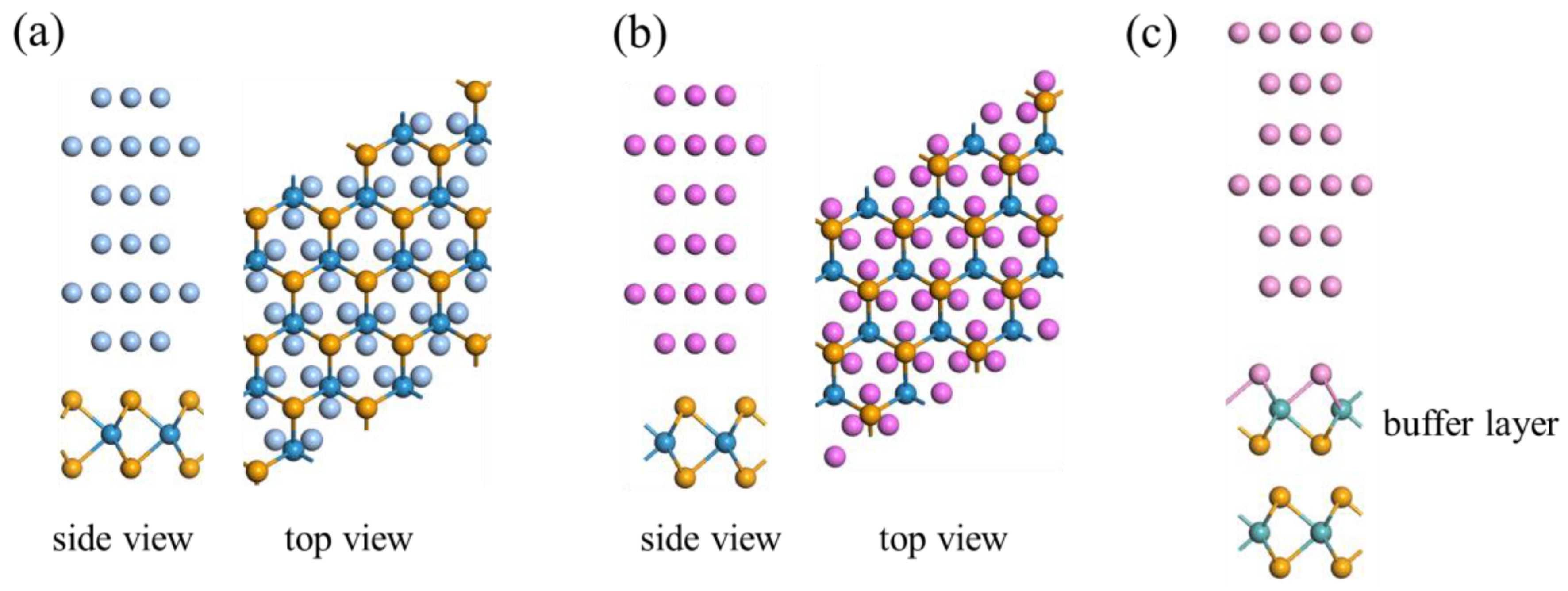
Figure 2.
Band structures of ML WSe2 contacting with several metal electrodes. The Fermi level is set to zero. (a)-(d) The bands dominated by metal atoms and ML WSe2 are plotted by gray and red curves, respectively. The Schottky barrier is marked in green and red.
Figure 2.
Band structures of ML WSe2 contacting with several metal electrodes. The Fermi level is set to zero. (a)-(d) The bands dominated by metal atoms and ML WSe2 are plotted by gray and red curves, respectively. The Schottky barrier is marked in green and red.
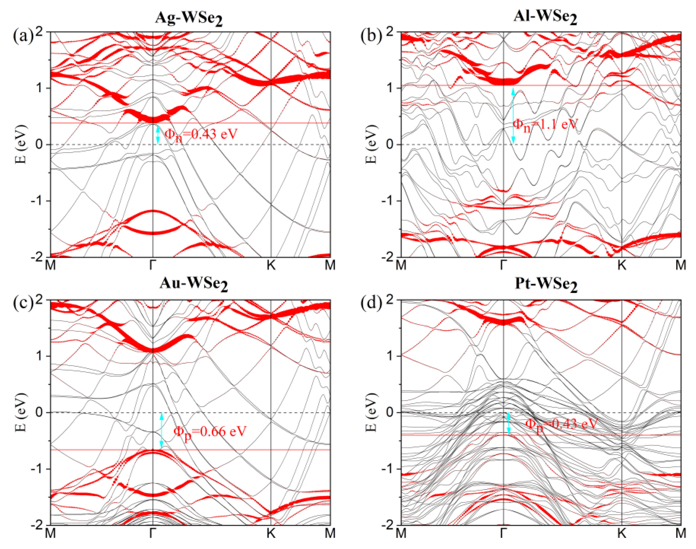
Figure 3.
Band structures of ML MoSe2 contacting with several metal electrodes. The Fermi level is set to zero. (a)-(d) The bands dominated by metal atoms and ML MoSe2 are plotted by gray and red lines, respectively. The Schottky barrier is marked in green and red.
Figure 3.
Band structures of ML MoSe2 contacting with several metal electrodes. The Fermi level is set to zero. (a)-(d) The bands dominated by metal atoms and ML MoSe2 are plotted by gray and red lines, respectively. The Schottky barrier is marked in green and red.
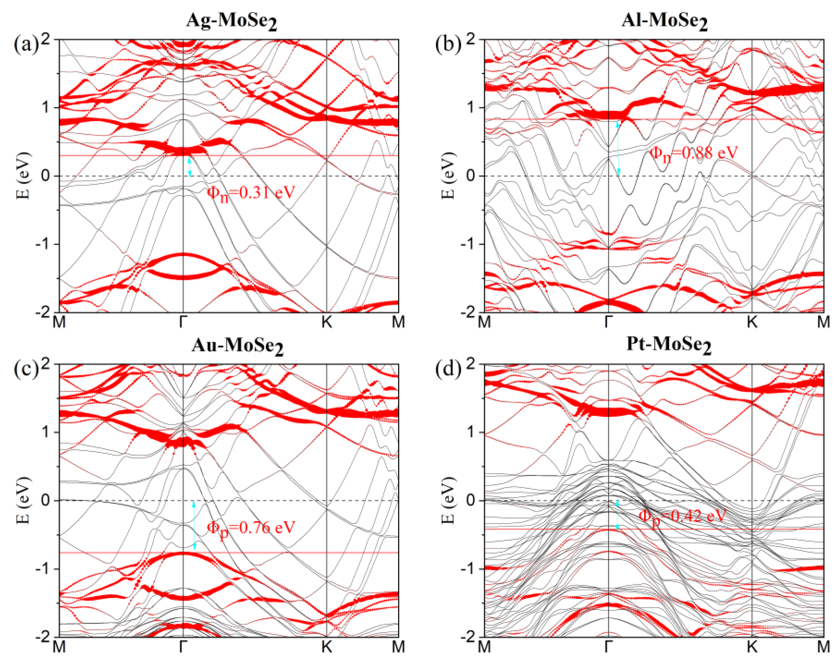
Figure 4.
Projected band structures of several metals contact to ML WSe2 with inserting mWSe buffer layers. The Fermi level is set to zero. Red line: energy bands dominated by WSe2 layer, gray line: band structures of metals-mWSe systems.
Figure 4.
Projected band structures of several metals contact to ML WSe2 with inserting mWSe buffer layers. The Fermi level is set to zero. Red line: energy bands dominated by WSe2 layer, gray line: band structures of metals-mWSe systems.
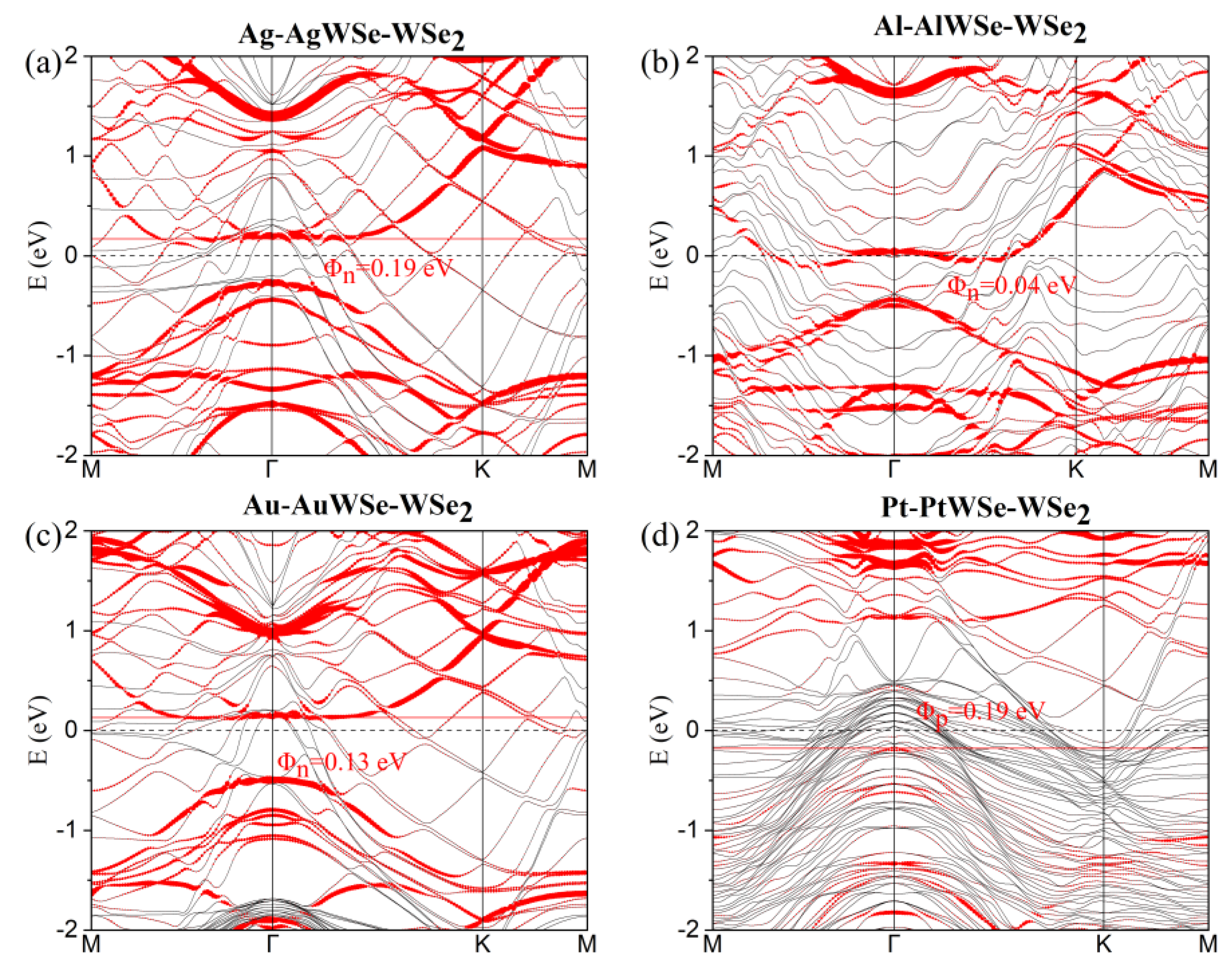
Figure 5.
Projected band structures of several metals contact to ML MoSe2 with inserting mMoSe buffer layers. The Fermi level is set to zero. Red line: energy bands dominated by MoSe2 layer, gray line: band structures of metals-mMoSe systems.
Figure 5.
Projected band structures of several metals contact to ML MoSe2 with inserting mMoSe buffer layers. The Fermi level is set to zero. Red line: energy bands dominated by MoSe2 layer, gray line: band structures of metals-mMoSe systems.
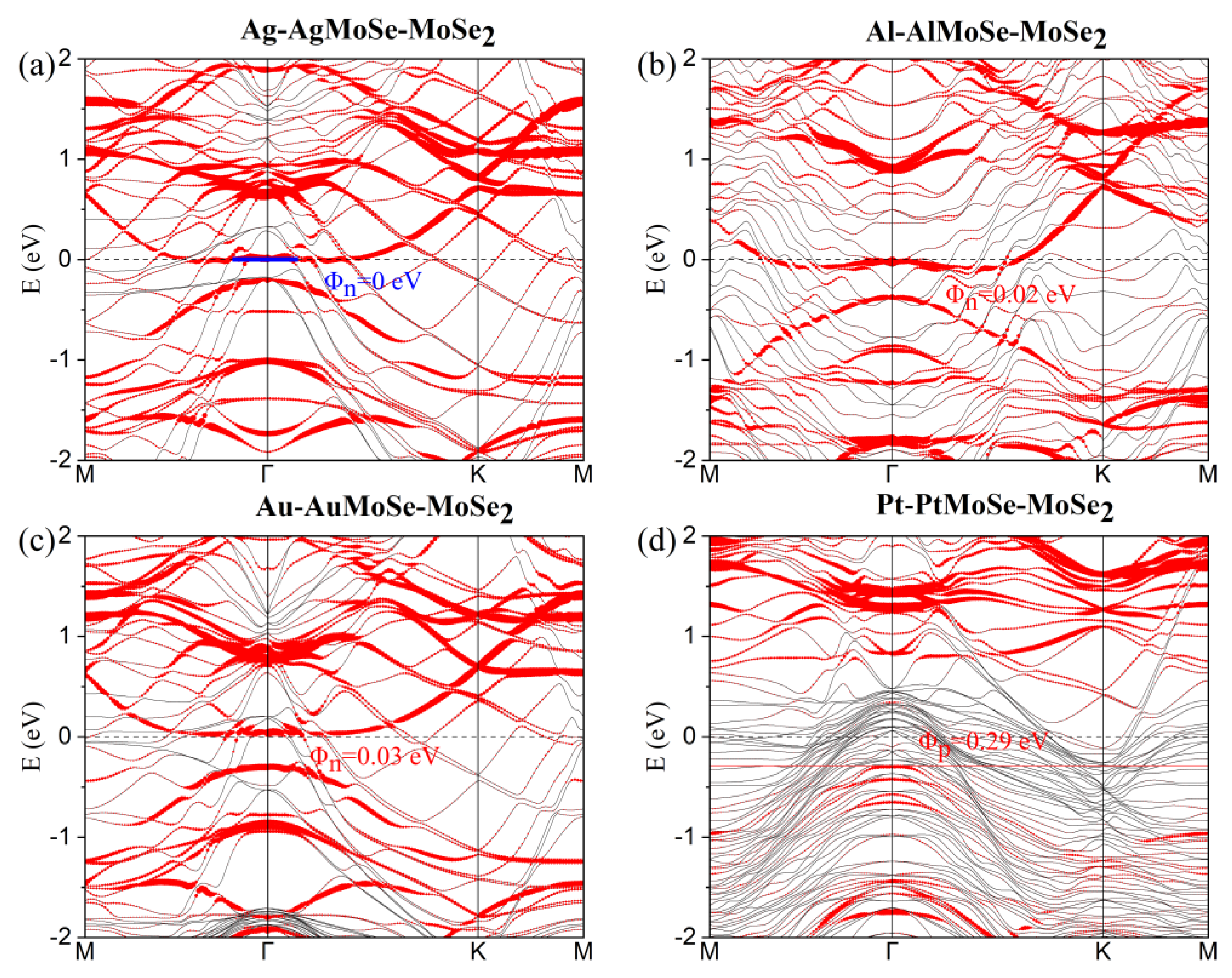
Figure 6.
Variation of the Schottky barrier height of electrons (Φn) with change of the work function for metals systems (a) in metal-MoSe2/WSe2 stacks and (b) in metal-mMoSe/mWSe-MoSe2/WSe2 stacks. The red and blue solid lines are fitted curves for metal systems contact to WSe2 and MoSe2, respectively. Fermi level depinning is seen after inserting a mMoSe/mWSe buffer layer, with pinning factors increased significantly.
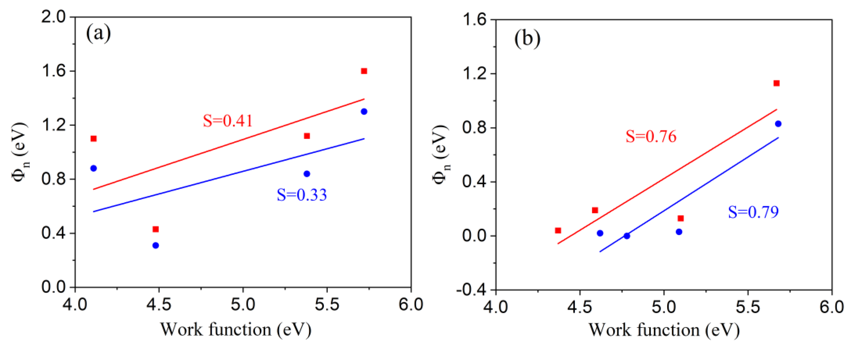
Figure 7.
Partial density of states (PDOS) of WSe2 after contact with (a)-(d) metals and (e)-(h) metallic mWSe surfaces for comparison. The Fermi level is at zero energy.
Figure 7.
Partial density of states (PDOS) of WSe2 after contact with (a)-(d) metals and (e)-(h) metallic mWSe surfaces for comparison. The Fermi level is at zero energy.
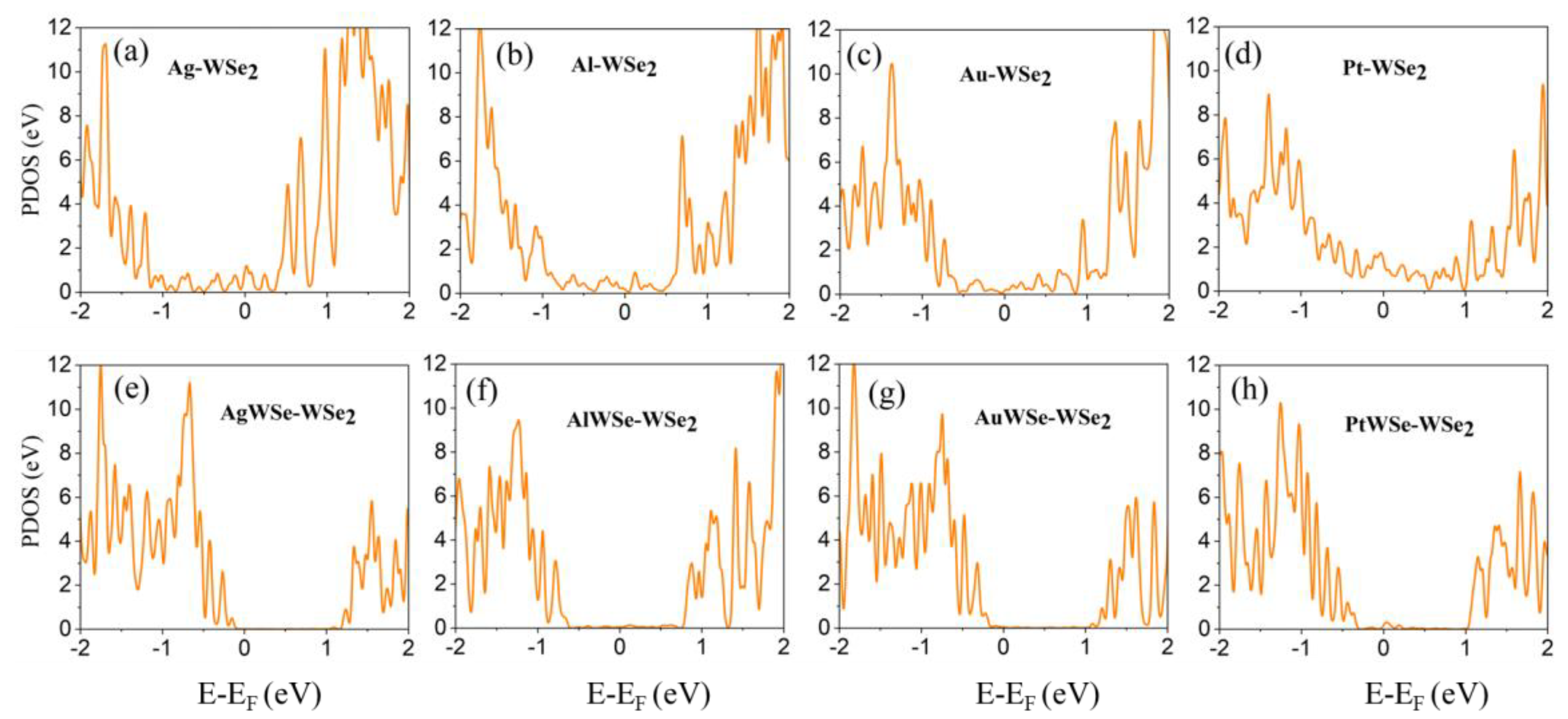
Figure 8.
(a) Schematic diagram of a MoSe2-WSe2 heterostructure device. (b) Simplified band diagram for metal-MoSe2/WSe2 contacts, the SBH and TB depend on the type of metal, which are related to the band hybridization degree. (c) Sketch of the band diagram for metal-mMoSe/mWSe-MoSe2/WSe2 stacks. The barrier height is reduced by suppressing the penetration of MIGSs.
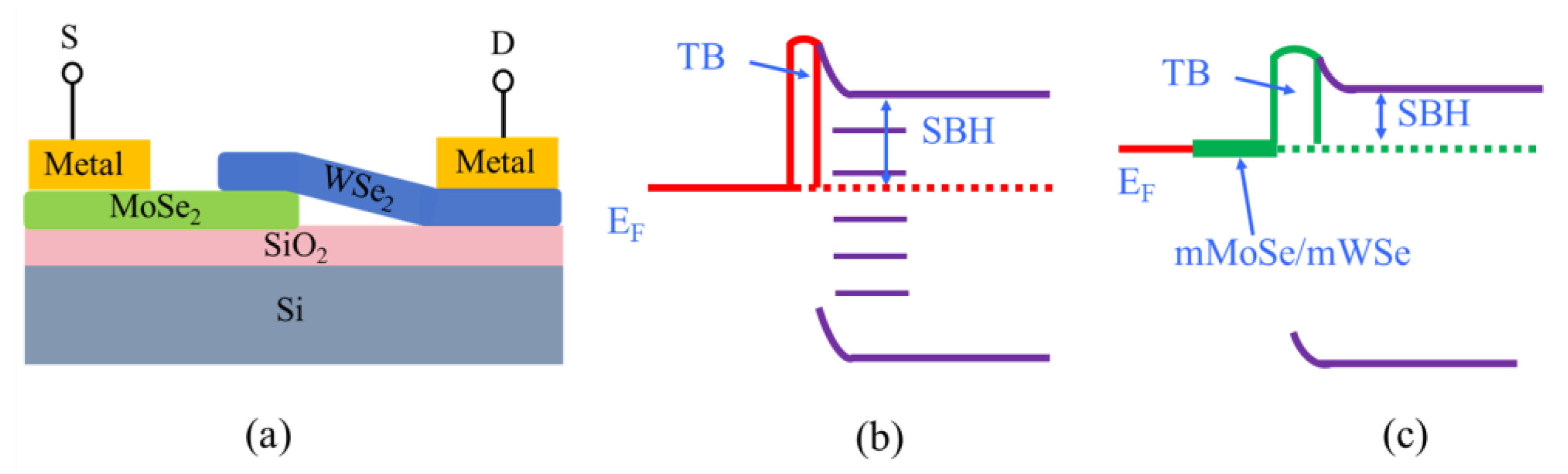

Table 1.
Calculated interfacial properties of WSe2 and MoSe2 on the metal electrodes. LM represents the lattice constant of the metals used in this article, with lattice mismatches in parenthesis below. dZ is defined as the physical separation (the distance between the Se atoms and the topmost metal atomic layer in the z direction). Eb is the binding energy. WM and W are the calculated work functions for clean metal and metal-WSe2/MoSe2 contacts, respectively. The SBHs extracted from band calculation without (with) inserting a buffer layer. (Nelectron Schottky barrier, Phole Schottky barrier).
 |
Disclaimer/Publisher’s Note: The statements, opinions and data contained in all publications are solely those of the individual author(s) and contributor(s) and not of MDPI and/or the editor(s). MDPI and/or the editor(s) disclaim responsibility for any injury to people or property resulting from any ideas, methods, instructions or products referred to in the content. |
© 2025 by the authors. Licensee MDPI, Basel, Switzerland. This article is an open access article distributed under the terms and conditions of the Creative Commons Attribution (CC BY) license (http://creativecommons.org/licenses/by/4.0/).
Copyright: This open access article is published under a Creative Commons CC BY 4.0 license, which permit the free download, distribution, and reuse, provided that the author and preprint are cited in any reuse.


