2. Material and Method
One factor to improve output in this research is the use of ultrasonic PWM from (20
500kHz) by using FPGA, which relied on the extent of voltage and the frequency from the sign utilized at the ultrasonic transducers, this is a novelty in this project, note that the FPGA is responsible for generating the signal with high accuracy. The choice of the frequency demand relies on the sort and the standard of required PWM [
4]. Ultrasonic PWM is defined as the voice waves which set frequencies behind the domain of a person's hearing [
5]. The chief standard in utilizing ultrasonic PWM is to ensure safe, to get high accuracy of the output power level, reduce the harmonic distortions (Low losses), and be more economical than the use of high frequency in an inverter, as well as used in the motor constant torque with speed variety by control of the amplitude of voltage and frequency to make to reduce torque pulsation in power switching.
The PWM effort can become rise till to undesired impact of the signals (harmonic distortion). The PWM efficiency and accuracy may be reductions occur if the used force is growing more than required without considering to components that may be used in the inverter. It can be concluded from the above paragraphs that controlling frequency, voltage, and power, as constant-time operation of the switching, have vital importance in designing ultrasonic PWM [
6,
7], with a high accuracy level on output and low losses through a design inverter. The proposal in this research is to use ultrasonic waves (UPWM) from (20 -500KHz) with the use of the positive phase sequence connected to compound splicing (CS) to improve the output with high accuracy and low losses, and control generation of UPWM by FPGA through field-oriented control (FOC).
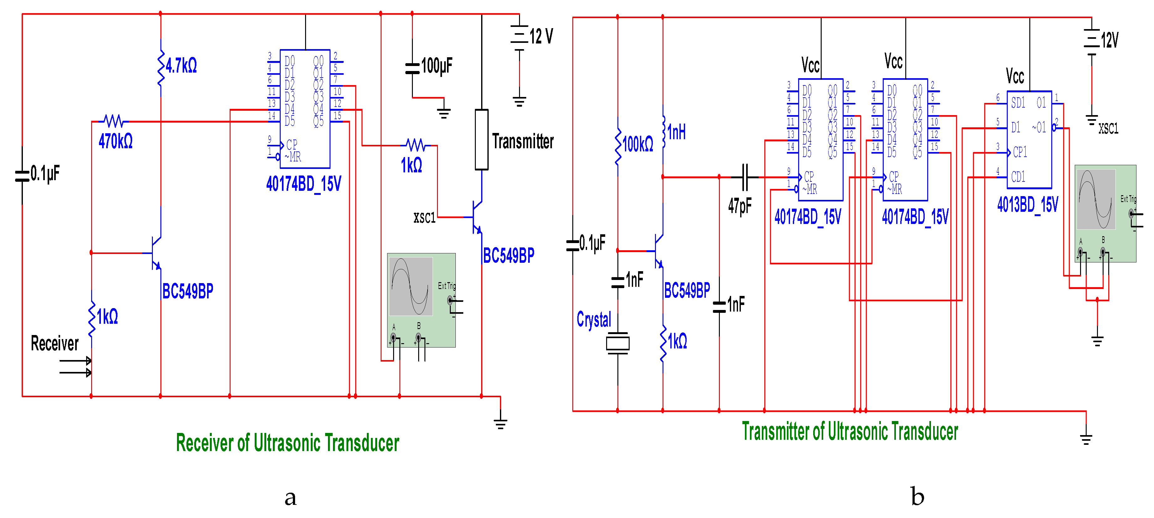
Pulse is maximum generally used through actions about a pulse generator circuit to provide integrally the system of high accuracy ultrasonic PWM generators. As well as, an oscillator circuit used as a microcontroller with 4GHz is a novelty. in this study, an ultrasonic PWM generator system is designed by using an FPGA technology controller see
Figure 1. The FPGA board is accountable for the reproduction of eight PWM digital signals into the lead for autonomous force operator collective programmable peripheral interface (PPI) type 8255A.
The hardware of this research includes digitally-controlled frequency and power units together by using an oscillator circuit proposed to control all the systems with the 4GHz.This proposed frequency has great benefits, including not to need use protection circuits from overcurrent and overvoltage that are excessive that cause surges that lead to damage to the device. As well as, reducing the size of the designed system.
The digital PWM signals obtained from FPGA implementation can securely and more reliably supply power to the MOSFETs in an inverter through the section for the ultrasonic PWM unit. The technical method used in an inverter changes the D.C. voltage to high-frequency waves through oscillator circuit control. Each three-phase transducer in the inverter has three ultrasonic transducers that have the same resonant frequency of nearly 100kHz. [
8,
9].
The remarkable thing is that every ultrasonic PWM can generate different frequencies, different powers, and at separate levels [
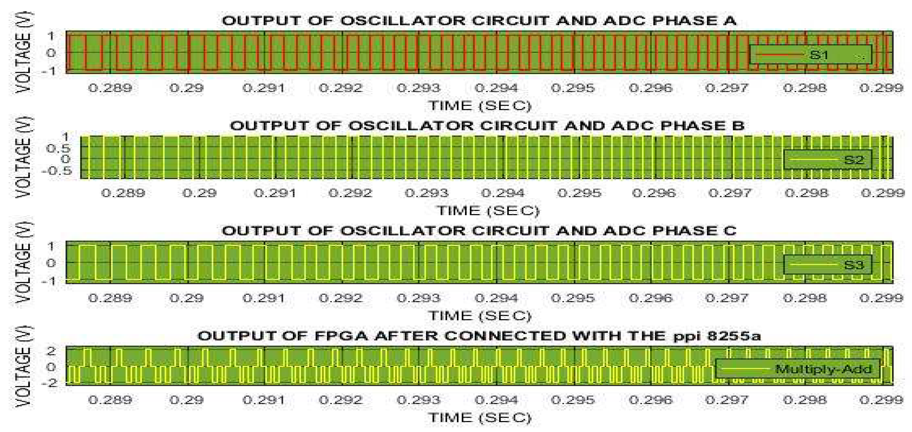
10]. Therefore, when designing, we can use only one unit of FPGA, which is based on a field-oriented control (FOC). Transistors provide power conversion at ultrasonic frequencies greater than (20 kHz). If allowed develop DC/AC converters with higher accuracy or efficiency, higher power density, lower output voltage distortion, and lower spurious sign standards in the audio frequency group. The accuracy of the output voltage waveform would be better when the value of the frequency ratio is very large since the unwanted harmonics in the output waveform move to the higher frequency region. The ultrasonically-modulated inverters offer several technical and economic advantages compared with PWM inverters which are switched at frequencies of a few kHz, while the carrier frequencies of ultrasonic PWM are in the large of 20 kHz to 100 kHz. As well as, there are advantages to this high frequency which are: (1) Very low harmonic distortion in the PWM synthesized waveform, (2) minimal acoustic noise in an inverter resulting in quiet operation, and (3) A simplified modulator system can be used with the fixed carrier frequency. See
Figure 1 and
Figure 2.
The second reason to improve production is to use compound splicing (CS) The foundation of the inverter's designed output filter is (LF, CF, and RL) [
11], When designing, it is important to minimize total harmonic distortion (THD) and ripple voltage (RV) at linear and nonlinear rectifier (RC) loads. Given its importance, the design of the filter has a very important role in reducing losses and increasing output accuracy, and it is considered a new work in conjunction with a positive phase sequence. The total of the values of the reactive power (Q) that can be produced in the inductive and capacitive filter is indicated by (LF, and CF), which should have required egalitarianism of interacting power coefficients.
Where,
is the load resistance,
is the switching frequency,
is the modulation index.
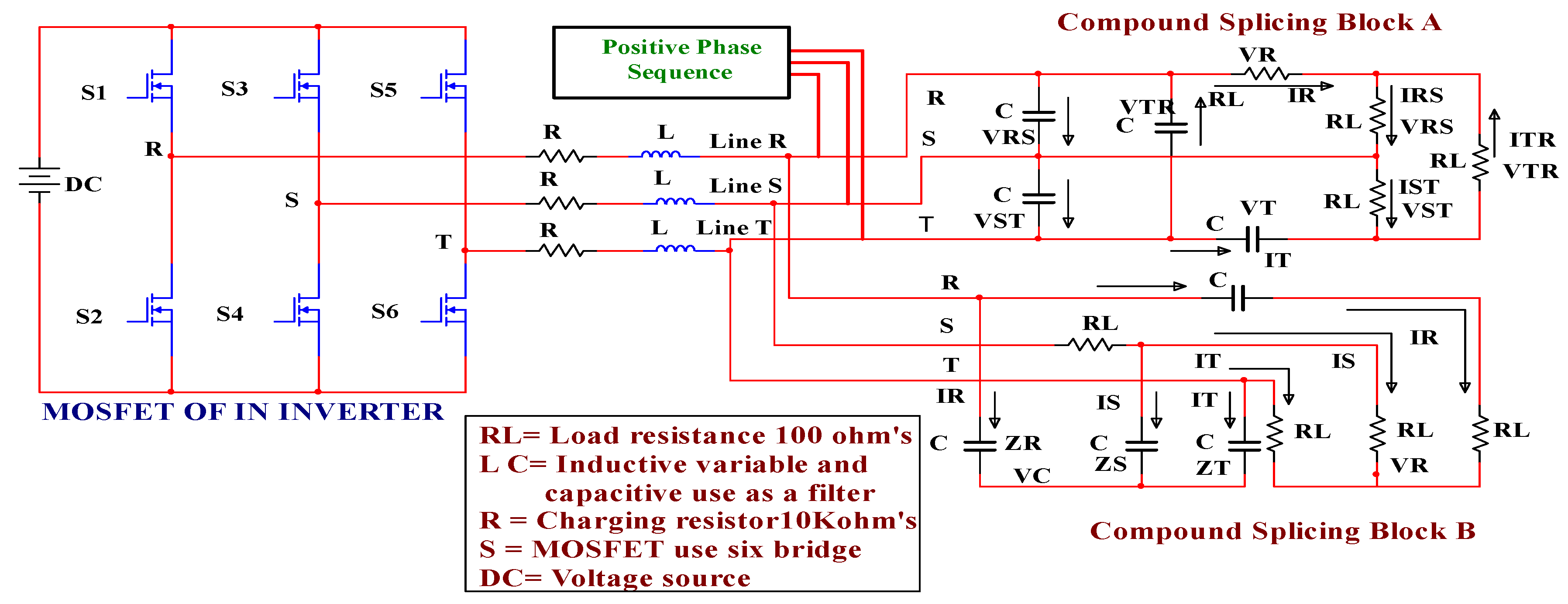
The compound splicing (CS) of balance load which is displayed in
Figure 3A,B) displays 4 lines egalitarian to PWM.
Ultrasonic PWM is advantageous for reducing the ripple voltage's (RV) amplitude, depending on the passive components employed. Given that the inductance serves as the current source, an excess current will mostly flow through the capacitor's (CF) filter, raising the output voltage. Therefore, it would appear that cutting would take longer in an inverter than switching ( ON-OFF), thus overtaking would be similar to the open circuit's work [
12,
13]. The output voltage controller's accuracy is at its highest for tiny modulation indices (M) due to the potential for a rise in the primary harmonics of an inverter output voltage that could result from (1-M) VDC. For lower productivity filter inductances, we should have a modest modulation index (M) so that the voltage controller in use is accurate enough. The voltage value above the filter inductor must be greatly raised when a nonlinear rectifier RC load starts to operate and pulse current starts to flow to the load capacitor. From equation (4), M appears at an extreme worth that is constrained [
14].
Controlling the modulation index (M) is one method for boosting voltage gain (Hertel et al; 2018), however doing so alters the duty cycle, which impacts losses. in this state, we must manipulate the (1-M) base, which has the potential to result in current ripples at low frequencies, to generate PWM with a significant jump in duty cycle support.
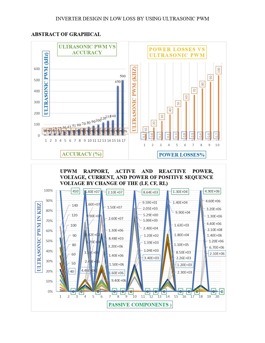
That the compound splicing (CS) in block A employs a portion of capacitors to define the redistribution of active power among the phases and compensate for most of the load's reactive power, also in part B the capacitors compensate for the active and reactive power on the other side, the crew load compensator can achieve the appropriate power factor and total stability. Contrary to the conventional compensation method, this is the new best technique. It will result in small size, reduced costs, elastic control, high accuracy (99%), and extremely low losses (0.11%). The correctness of the system is observed using the MATLAB, Simulink application. It has been found that the system's precision and low losses depend on passive components; this depends on UPWM, and the compounds of (LF, C F, and RL) change in value in response to ultrasonic PWM.
Table 1., makes it evident that the values of the passive components (CL, LF, and RL) depend on the accuracy and losses of the ultrasonic PWM signal.
Due to the triple harmonics that result from the neutral point's incidence, an inverter's PWM needs to be modified [
15]. For voltage and current variables, A balanced load of matrices was shown in equation (5).
The constant and sync framing αβ is offered by converting the matrix as follows:
Where: ω is the grid frequency, αβ is the evidence of the constant shape, and the positive and negative shapes (voltage and current) denote the series of synchronous shaps in the positive sequence voltage.
Where: The positive-phase sequence is signified in
. The relation between line-to-line voltage and a
neutral point for the grid is specified via the following:
The voltage control of the DC abilities depends on the equipped input design. The immediate and medium energy losses worth are calculated as follows.
Positive sequence voltages:
Negative phase sequence voltages:
It might note from equation (8) that they are not stable, and based on this, the proposition utilized in the search is to locate the duration of the switching frequency by mutable the worths of the Lf, Cf. thus the duty cycle of ultrasonic PWM is controlled, and after that, these worths can fulfill demands for high accuracy and low losses.
The power of every phase is 1 to 3 of the gross energy production. The Clark transformation is signified as follows.
The merit of utilizing αβ and dq in the constant shape is to disconnect axes from a mutable, the control of the constant shape is carried out via the phase shift by (90
0) of two sine waves, with the reference voltage, but be an obstacle when the reference voltage is unsteady with frequency. Park transformation at constant αβ and dq wording also uses ωk as the angular basic frequency of the output.
Lastly, power equations signal that the balance of the product is caused via the balanced of LF, and CF, by the alterations that amount are restricted, thus, the synchronous UPWM with active of FPGA, filter design, and microcontroller by an oscillator circuit, gave positive results through high accuracy and low losses.
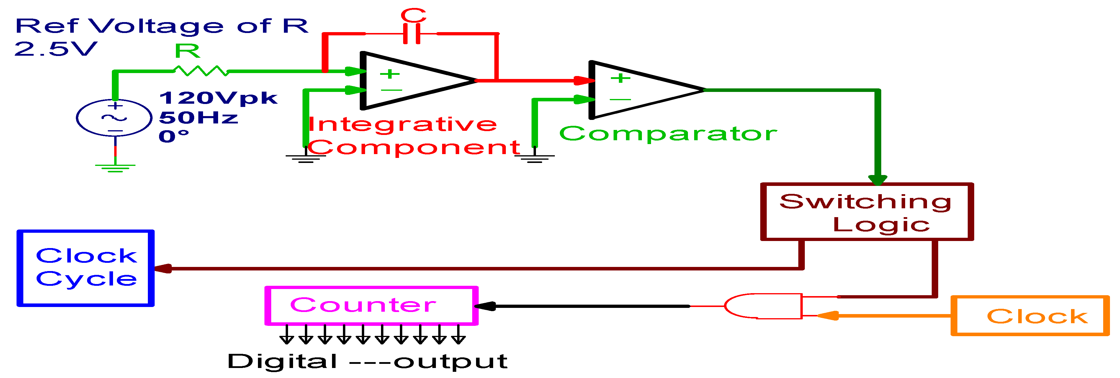
The third factor to improve output is the design of the ADC circuit was used to control the output by determining the value of the input voltage as well as to maintain the continuity of the voltage flow to the LC tanks in conjunction with the inverter work and thus it enhances the work of the MOSFET through the continuity of the voltage flow regularly, in addition to feeding the FPGA in digitally of bits sequentially [
15]. Thus ADC transforms voltages through a few input bandwidths, and it rejects distortion in high frequencies, also its work is slow. It is characterized by its high accuracy through fastening of modulation frequency at 50Hz or 60Hz, a little current is used and it is desirable in different uses [
16]. See
Figure 4.
The dual-slope of the ADC circuit through
Figure 4, is comprised of logic switching, an integrator circuit, comparator it works as a comparison between the input voltage and the reference voltage. The clock cycle, displays the time needed to measure the input voltage, the unknown voltage identified in the integration circuit and it represents the reference voltage. The switching works by the difference between the measured voltage and the reference voltage. The process is repeated by the integration circuit by unloading the capacitor charge bound in parallel with the integrator component. The conversion of the dual slope is in two stages, the first is run-up, which is called the (counting up) phase, and the second stage is run-down, which is called the phase (counting down). Through run-up, the provider of voltage to the integration component by the input voltage, in this case, the voltage supply of the integration component is chosen by the switch of action. Then, the integration components permit charging the capacitor for a specified period, for the run-down, the input voltage to the integration component is through reference voltage, i.e. the voltages are negative, and the reference voltages value is chosen by the integrator component based on to the switch devices. The integrator time of the output unit in this phase is zero. When the input voltage value is constant, the integrator component output appears in the following equation. [
16,
17].
Where: Vo is the output voltage Vref is the reference voltage, Vi is the input
voltage R and is the resistor and capacitor, , initial supplied voltage, , initial time.
The fourth factor in improving the output is the use of 4GHz frequency in the oscillator circuit to control the operation of the system without the need for external control components. This leads to a small size of the device, high accuracy, and low losses through the use of an external LC circuit, and RL slow charging circuit to increase the accuracy of the inverter work and increase the control. See
Figure 5.
3. Results and Discussion
The oscillator circuit used a clock frequency of 4GHz, in this case, all the operations of an inverter are controlled in real-time, the design of the Ultrasonic PWM inverter system uses the frequency ratio changing technique to use minimize the unwanted harmonics. Through the results in
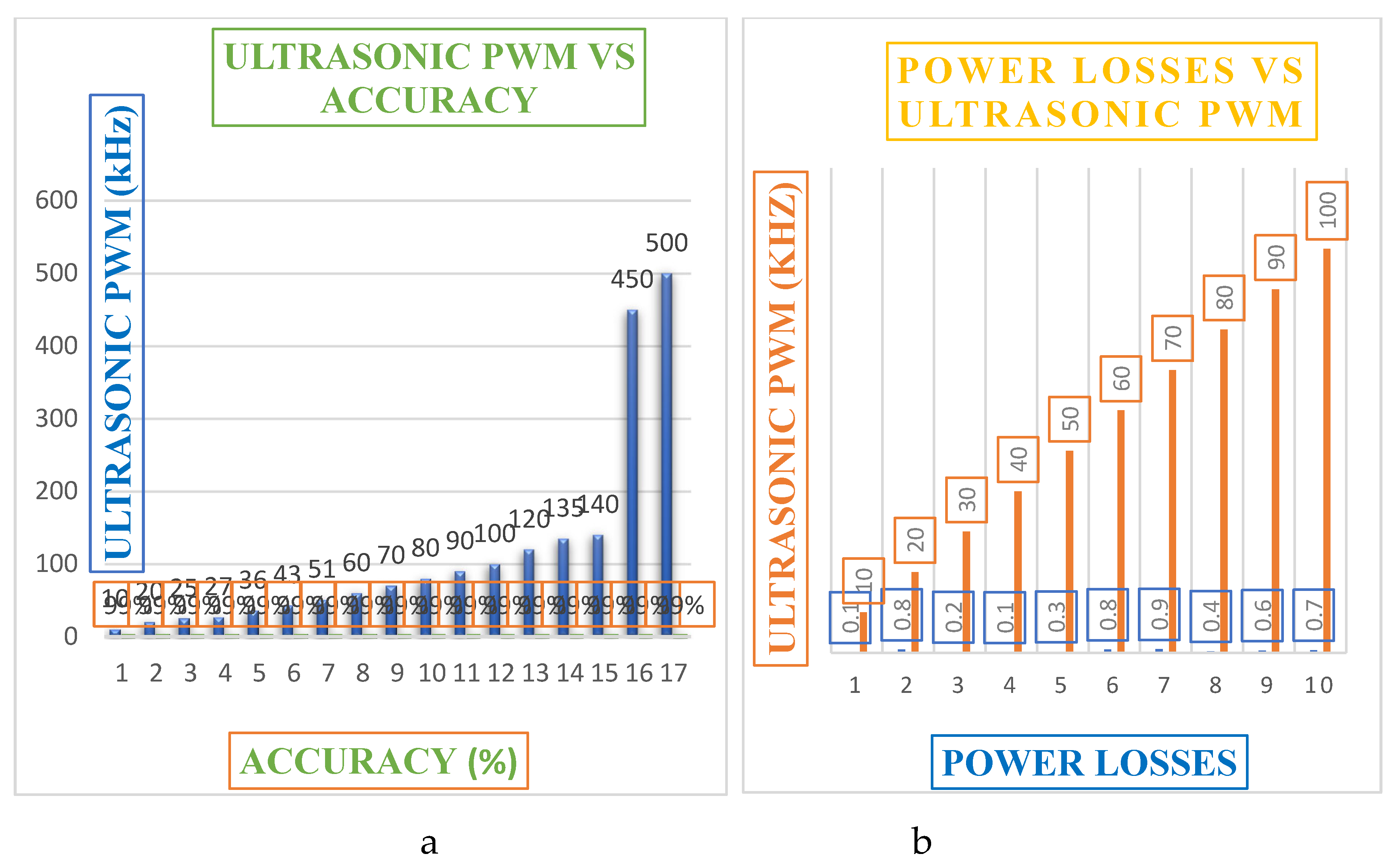
Table 1., note the effectiveness of the passive components in generating ultrasonic PWM in the output system, note when 20kHz, 30kHz, and 90kHz been obtained a high accuracy is 99%, and few losses of THD is (0.1%
, this is meaning that the medium energy of
switching losses (EMS) is low, as the switching losses depend on the input
voltage (Vi) and output of current (Io), as well as the switching frequency (
) and time that determines the work of switching
between turn-on (t2+t3) and turn-off (t5+t6). See equation (16), and see
Figure 6.
Where: is the medium energy of switching losses, is the switching frequency.
medium energy of conduction losses (EMC) is tiny because it depends on the output current (Io), RDS is the resistance of drain-source of a MOSFET, and duty cycle. see equation (17)
Whereas
Where:
energy in a turn-on,
Drain current in a turn-on,
Drain voltage in a turn-on,
rise time of current in a turn-on, and
fall time of voltage in a turn-on
If
is very small thus the energy off is:
Whereas
We conclude from equation (16). This raise in the switching frequency results in a rise in the medium energy switching losses. The medium switching energy loss is relying upon turn-on and turn-off periods, and the medium switching losses is too rely on the switching frequency, While, the conduction losses of equation (17) rely on the duty cycle (D).
The principle treatment that has been worked on in this research is to raise the ultrasonic PWM value from (20kHz-500kHz), to reduce losses and increase accuracy in conjunction with the compound splicing of output via the use of positive phase sequence to compensate for the losses that may occur from the generation of the magnetic field due to increasing the current in the inductance, and thus the generation of the parasitic capacitance, which leads to a occur a high degree of heat and increase the RDS(ON), and after that works to stop the inverter. Also, the design of the ADC gave an impetus to control the input voltage and compare it with the reference voltage, and thus the distortion was controlled to the very smallest possible value.
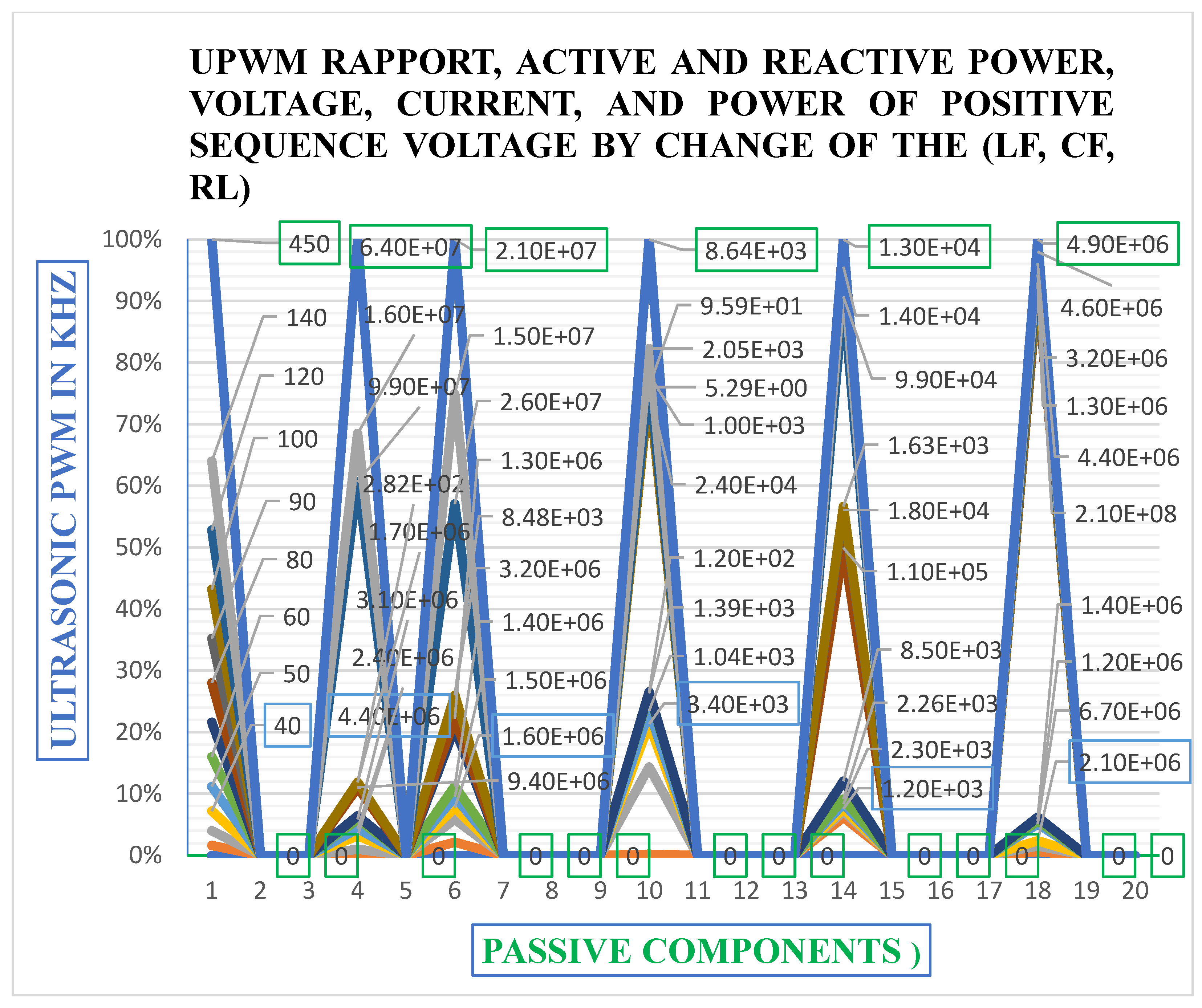
That utilizing the UPWM from (20—500khz) to acquire the necessary power and the voltage and current between phases, it has become an urgent necessity to improve the work of the inverter in this project thus positive voltage sequence, was employed at active power (P) of 6KW and reactive power (Q) of 3KVAR. Demonstrates that compound splicing using the three-phase dynamic load and synchronous with ultrasonic PWM and FPGA to produces high accuracy and low losses. Knowing that the three-phase dynamic load has been modified in the frequencies (120-500kHz) to an active power (P) of 8KW and a reactive power (Q) of 6KVAR at the frequencies of 120 kHz, 135 kHz, 140 kHz,450 kHz, and 500 kHz to acquire the necessary power, were to extend the period of switching frequency for to avoid interference between current and voltage, see
Table 2.
Figure 7.
Shows the values of UPWM, active power, reactive power, voltage, current, and the power of positive sequence voltage by the change of the passive components.
Figure 7.
Shows the values of UPWM, active power, reactive power, voltage, current, and the power of positive sequence voltage by the change of the passive components.
Figure 8.
a-shows ultrasonic PWM vs: a- accuracy; b- power losses.
Figure 8.
a-shows ultrasonic PWM vs: a- accuracy; b- power losses.
Figure 9.
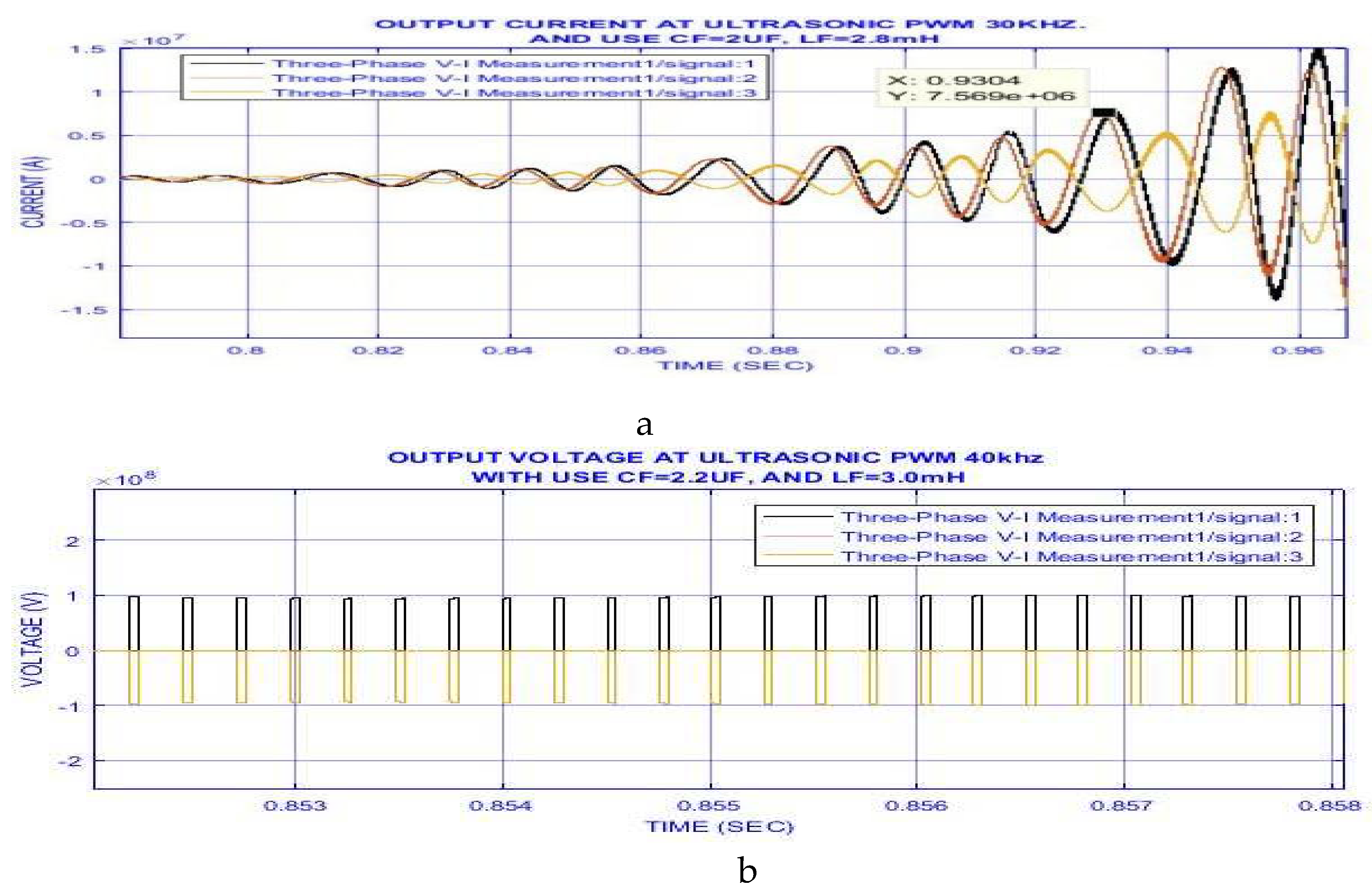
Output when using UPWM of 30kHz; a- current, b- voltage when using UPWM of 40kH.
Figure 9.
Output when using UPWM of 30kHz; a- current, b- voltage when using UPWM of 40kH.
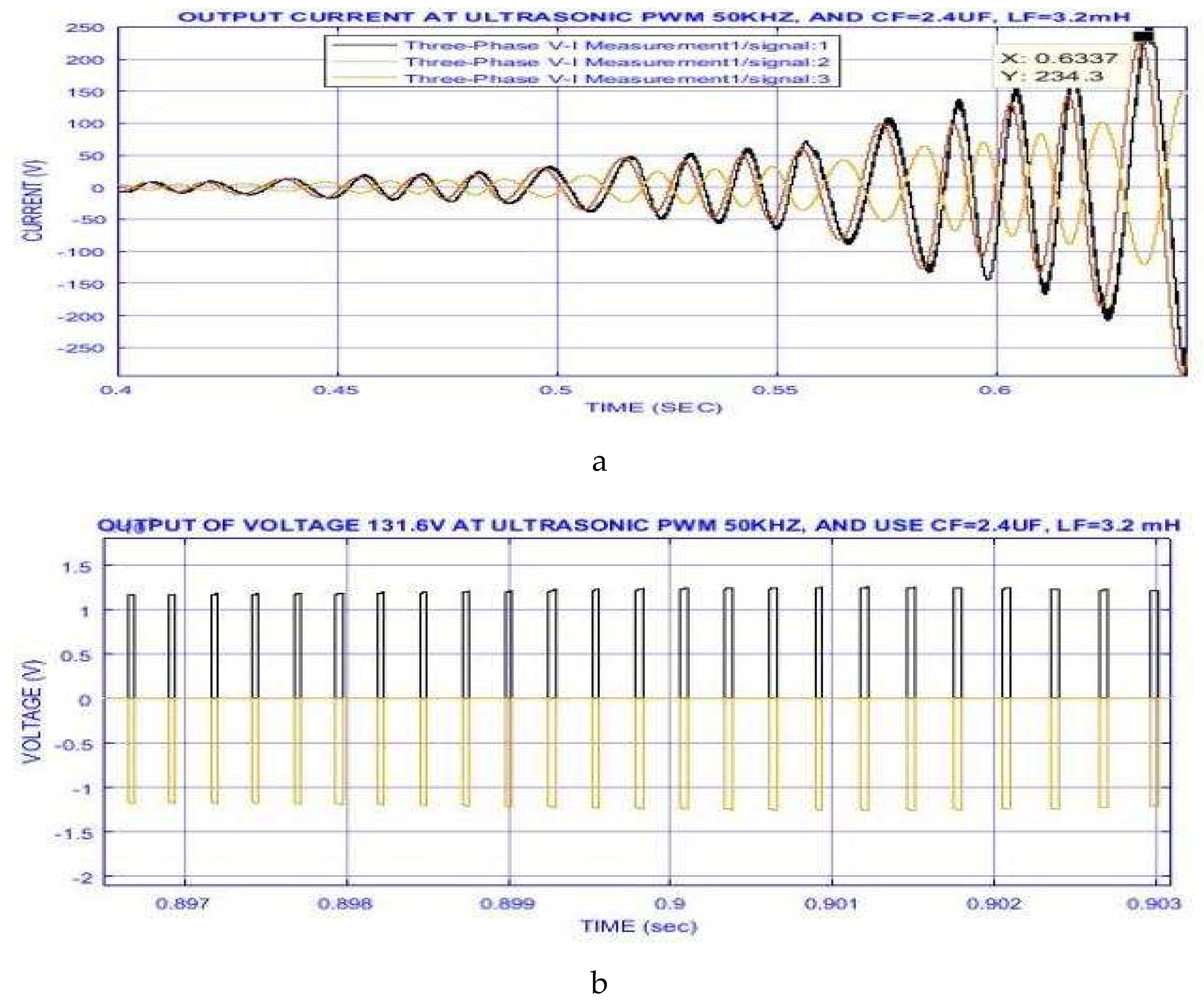
Figure 10.
Shows the output at UPWM of 50kHz: a- current; b- voltage.
Figure 10.
Shows the output at UPWM of 50kHz: a- current; b- voltage.
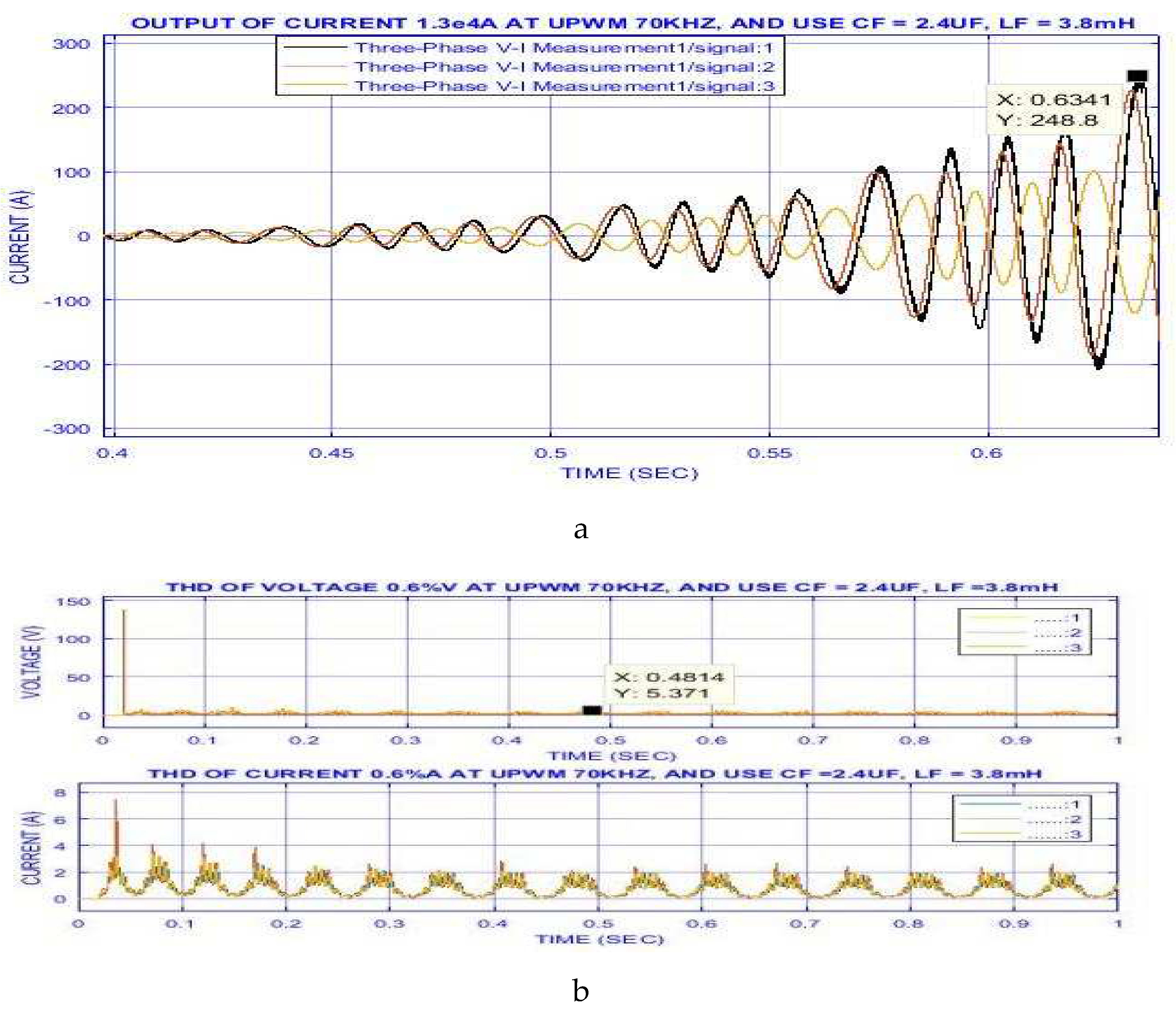
Figure 11.
Shows of output at UPWM 70kHz: a- current b- THD is 0.6%.
Figure 11.
Shows of output at UPWM 70kHz: a- current b- THD is 0.6%.
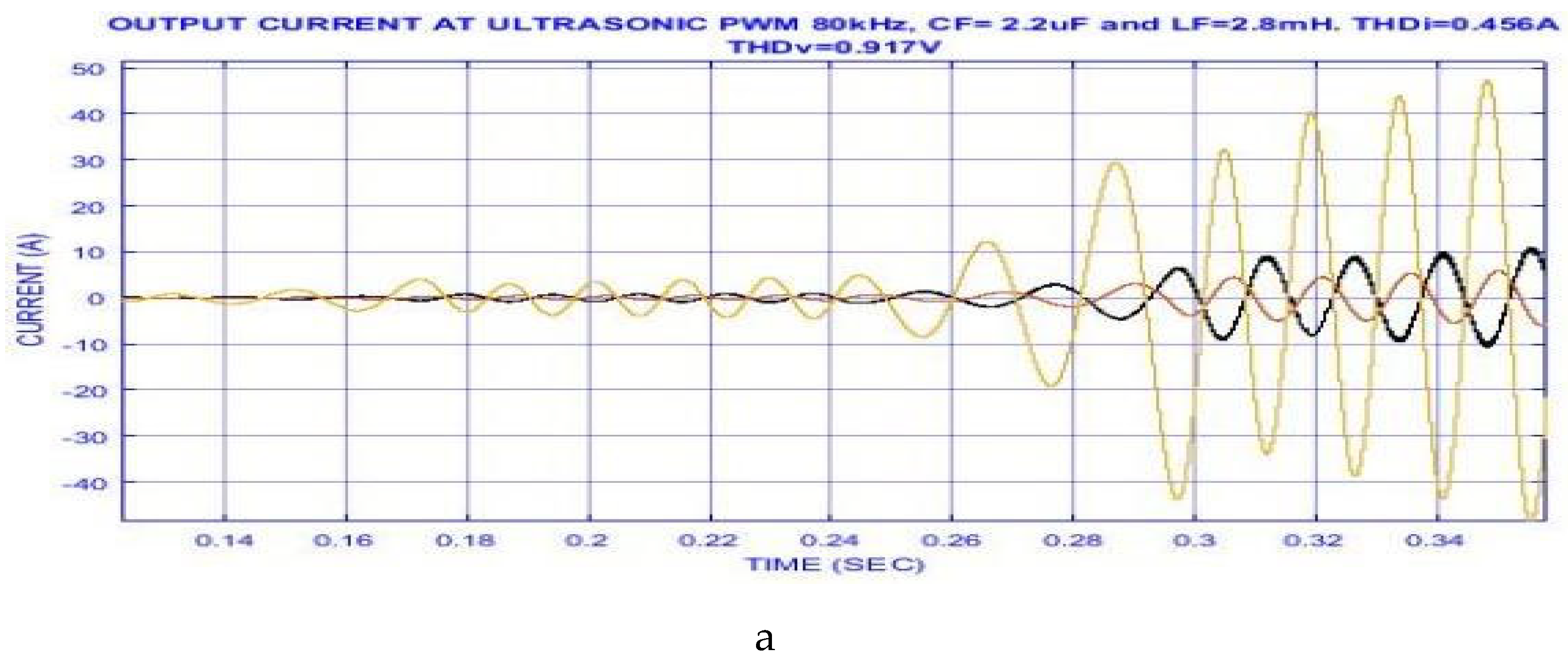
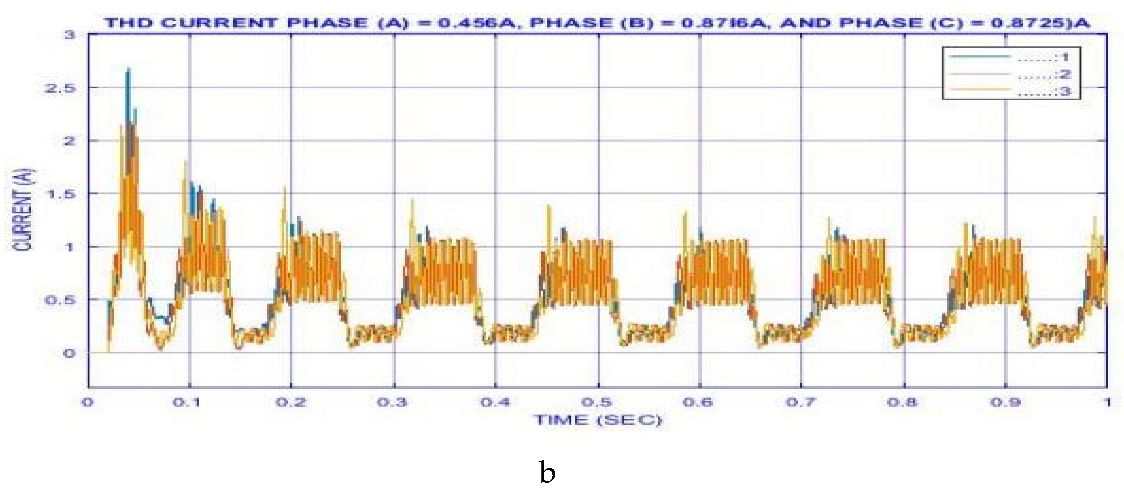
Figure 12.
The output at UPWM is 80kHz; a- current. b- THD.
Figure 12.
The output at UPWM is 80kHz; a- current. b- THD.
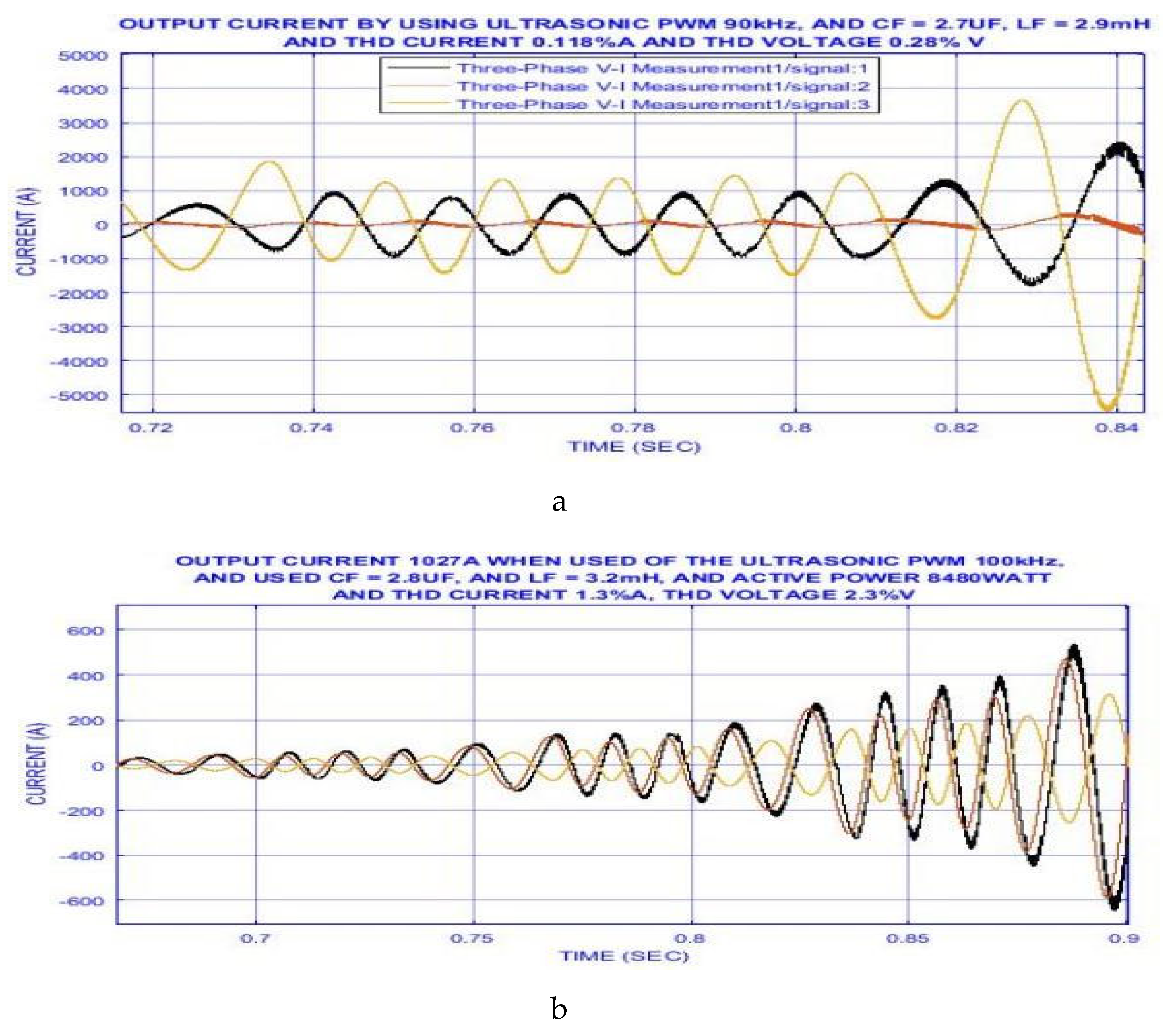
Figure 13.
a- shows the output current with UPWM is 90kHz; b- shows the output current when using UPWM at 100kHz.
Figure 13.
a- shows the output current with UPWM is 90kHz; b- shows the output current when using UPWM at 100kHz.
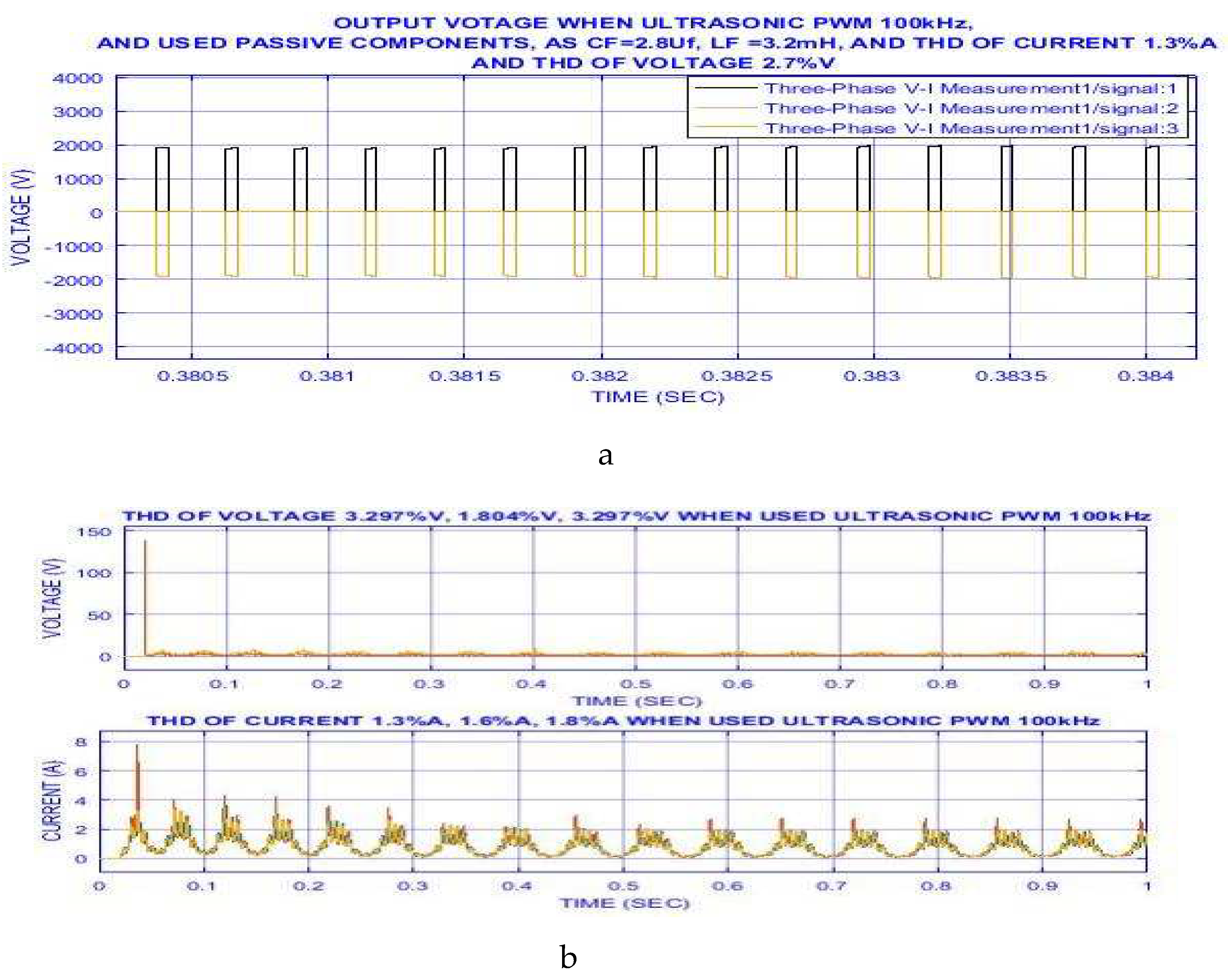
Figure 14.
Output when using UPWM at 100kHz: a-voltage. b- THD.
Figure 14.
Output when using UPWM at 100kHz: a-voltage. b- THD.
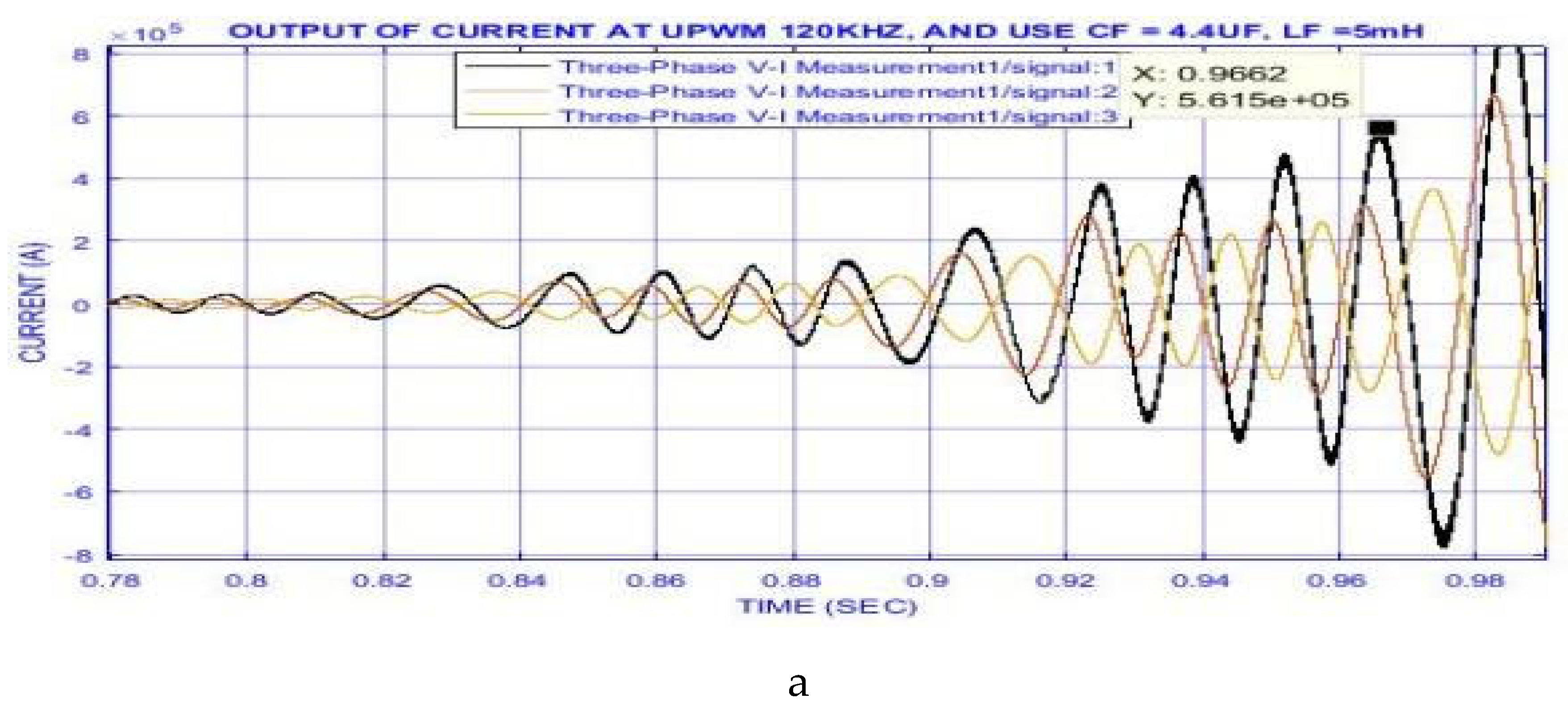
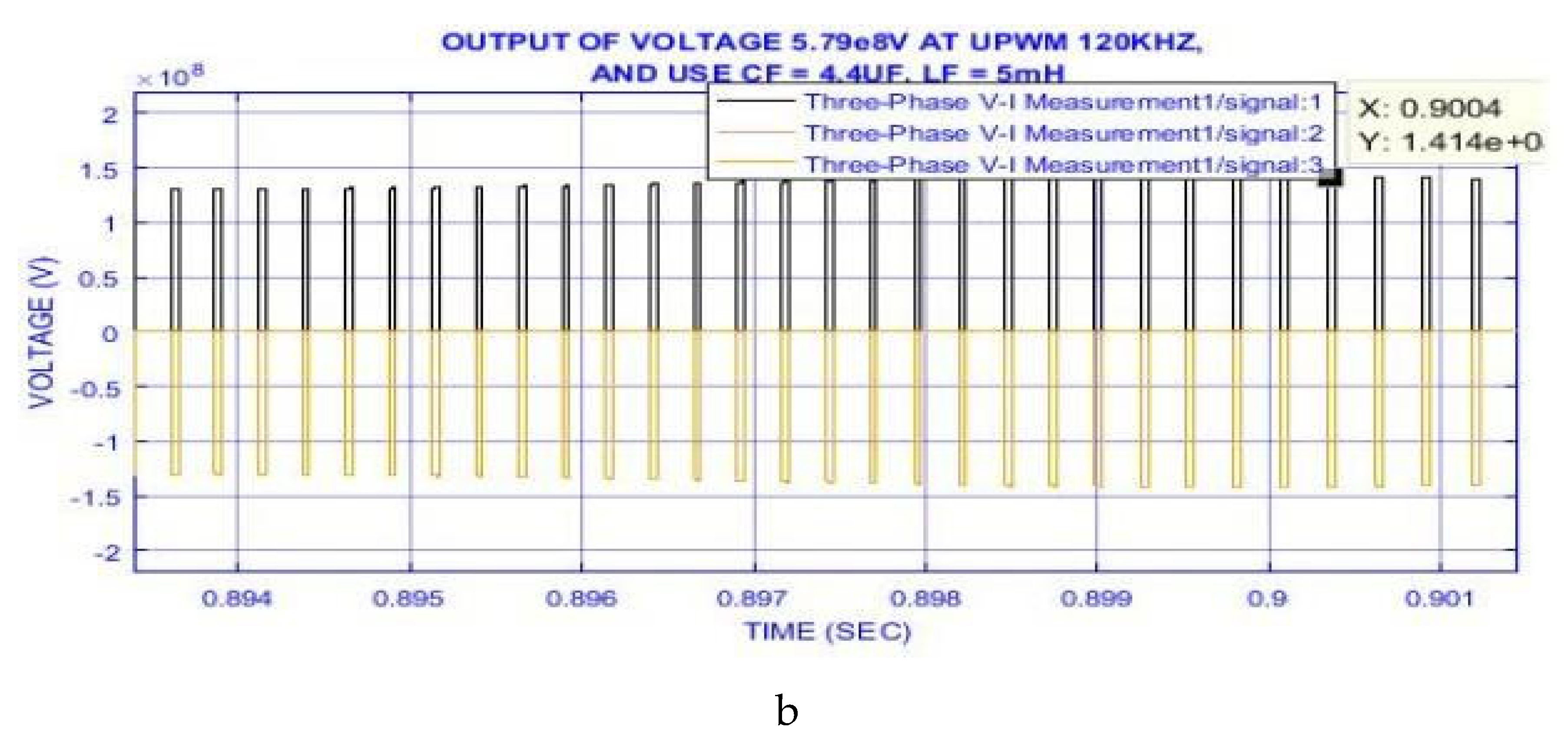
Figure 15.
The output when using UPWM is 120kHz, a-.current, b- voltage.
Figure 15.
The output when using UPWM is 120kHz, a-.current, b- voltage.
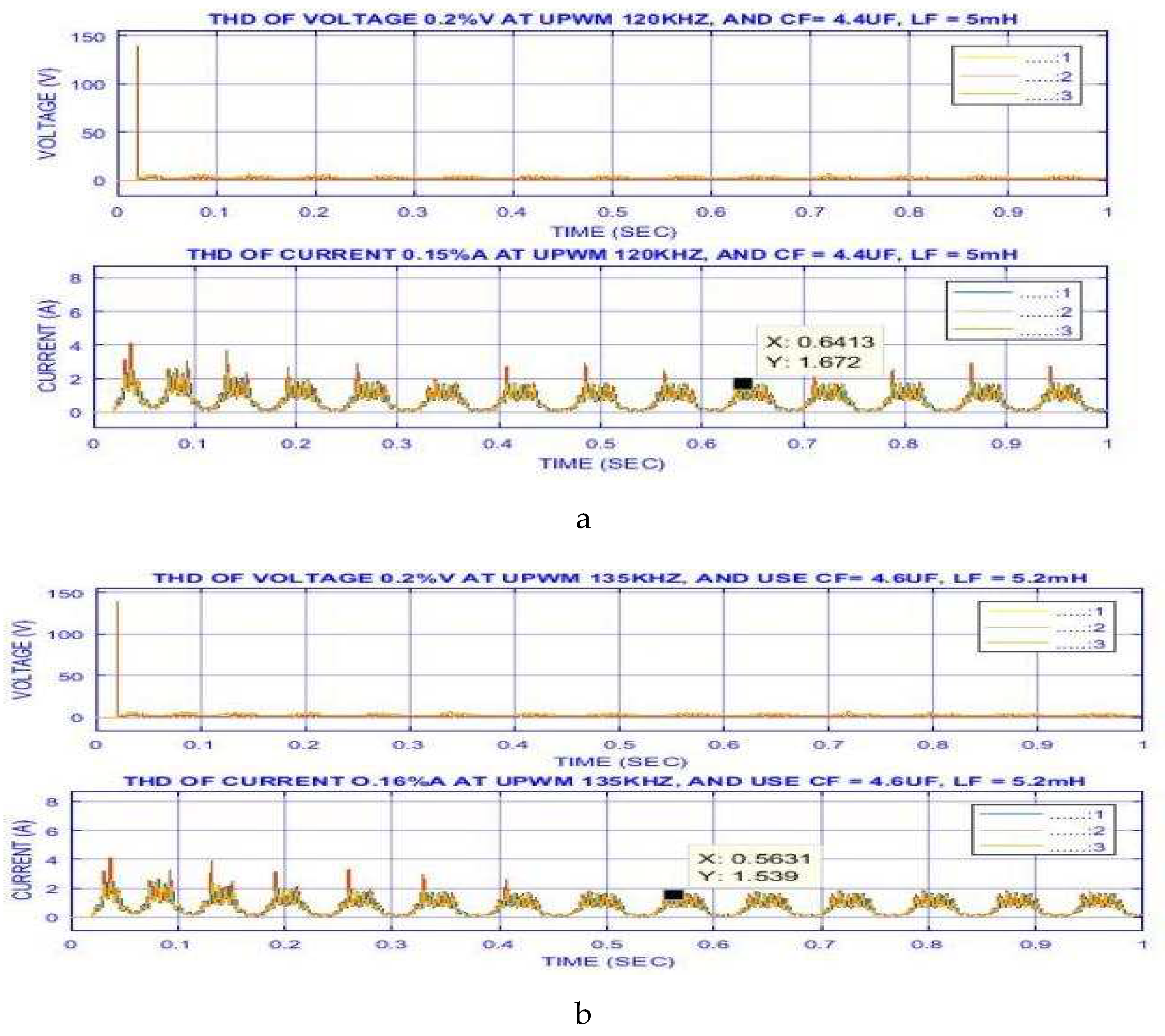
Figure 16.
a- UPWM at 120kHz; a- THD is 0.1%; b- UPWM at 135kHz THD is 0.16%.
Figure 16.
a- UPWM at 120kHz; a- THD is 0.1%; b- UPWM at 135kHz THD is 0.16%.
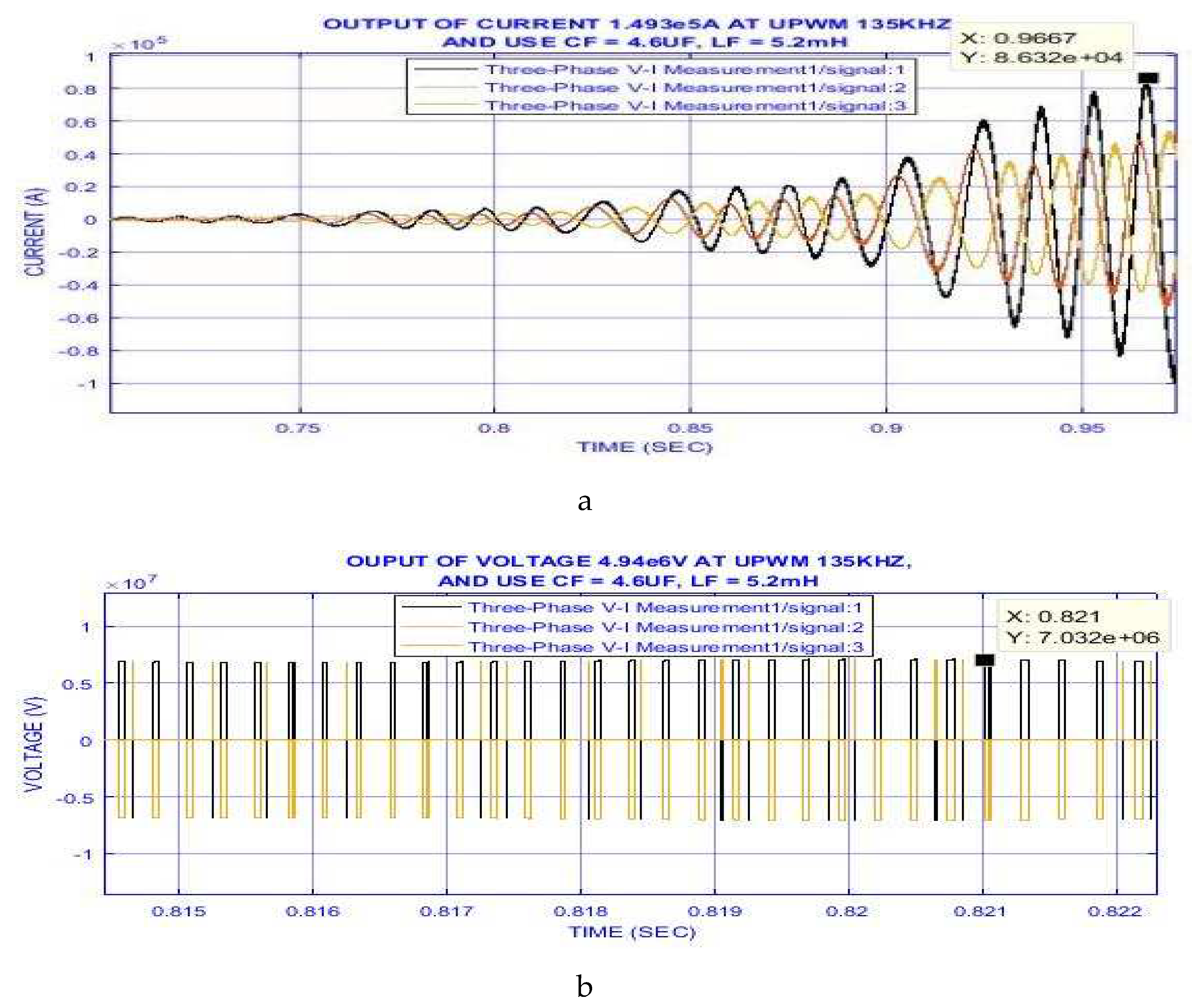
Figure 17.
The output when using UPWM of 135kHz; a- current; b- voltage.
Figure 17.
The output when using UPWM of 135kHz; a- current; b- voltage.
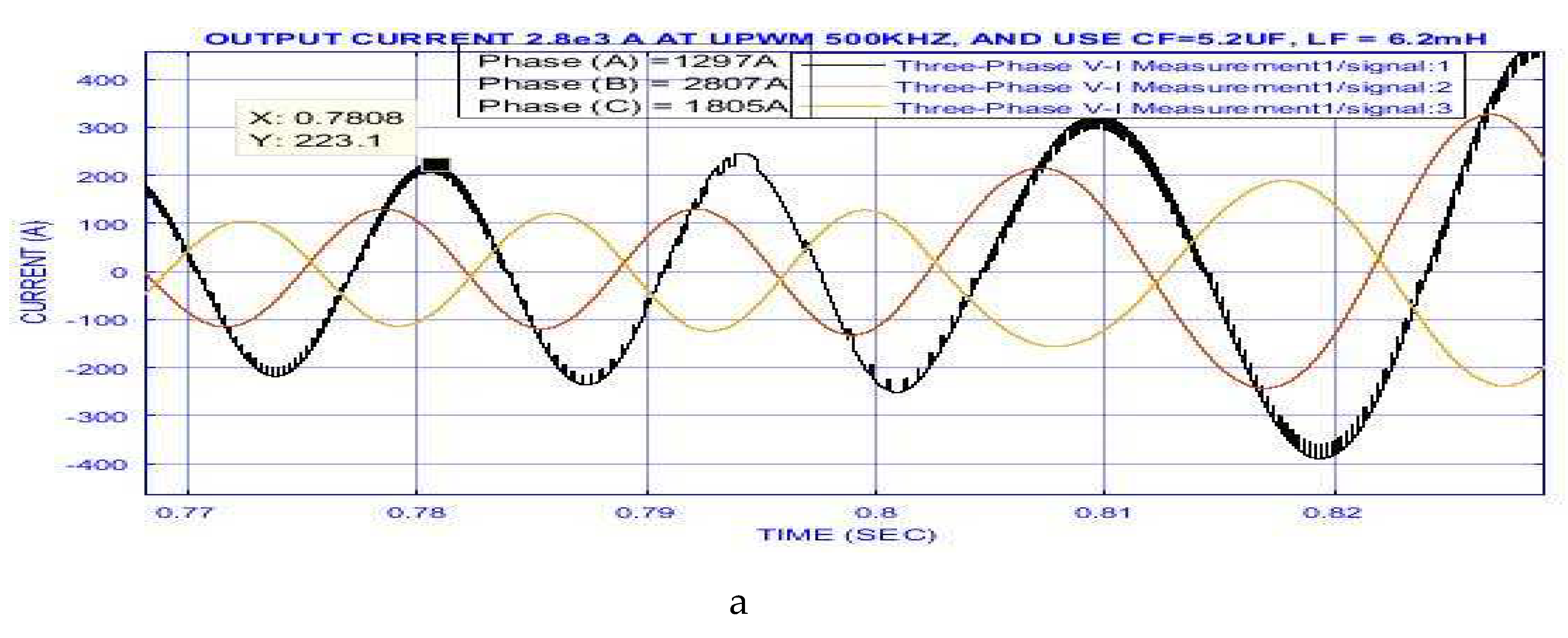
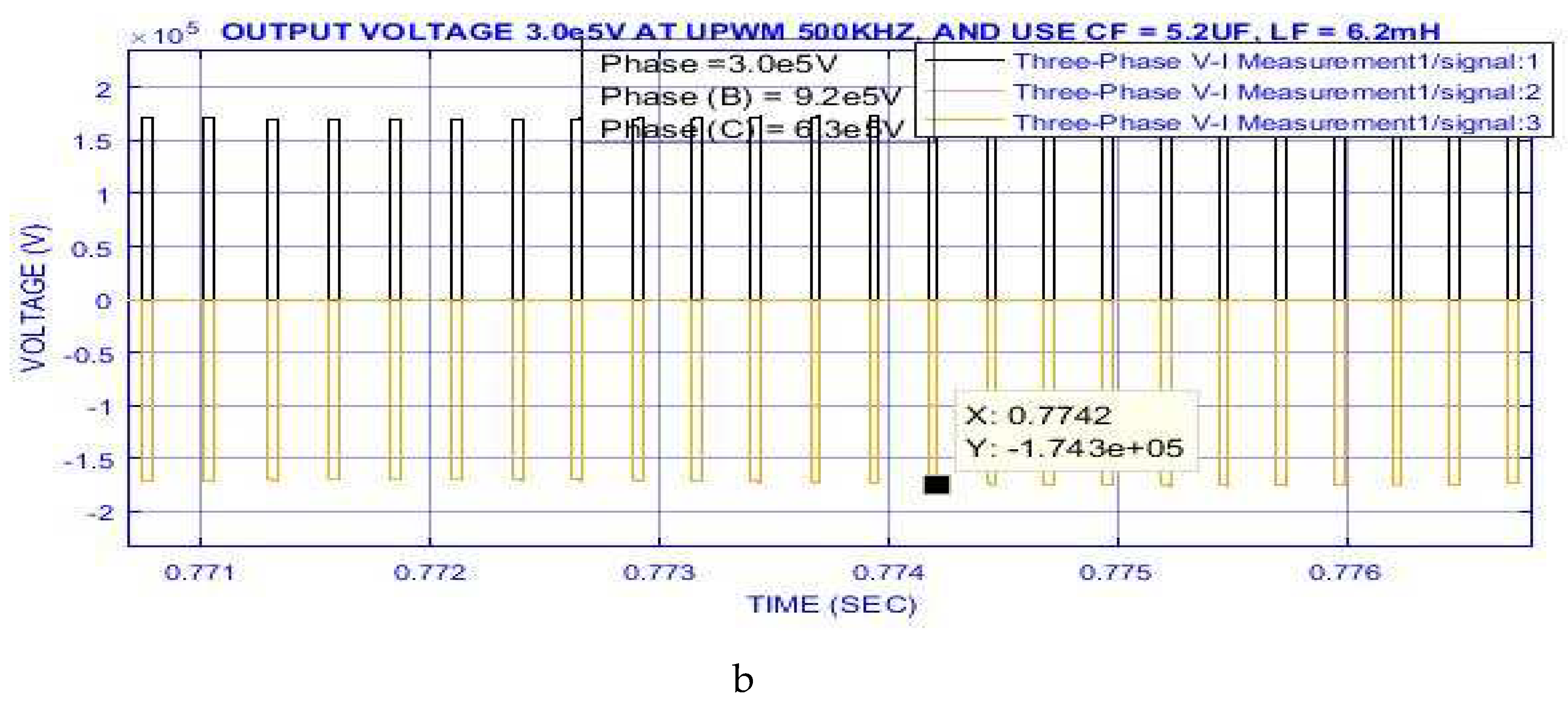
Figure 18.
The output when using UPWM of 500 kHz; a- current; b- voltage.
Figure 18.
The output when using UPWM of 500 kHz; a- current; b- voltage.
