Preprint
Article

Semiconductor-to-Insulator Transition in Inter-electrode Bridge-Like Ensembles of Anatase Nanoparticles under a Long-Term Action of the Direct Current

Altmetrics

Downloads

105

Views

55

Comments

0

A peer-reviewed article of this preprint also exists.

Submitted:

10 April 2023

Posted:

11 April 2023

You are already at the latest version

Alerts
Abstract
The results of experimental studies of ohmic conductivity degradation in the ensembles of nanostructured anatase bridges under long-term effect of direct current are presented. Stochastic sets of interelectrode partially conducting bridges consisting of close-packed anatase nanoparticles were formed by the seeding particles from drying aqueous suspensions on the surfaces of silica substrates with interdigital platinum electrodes. Multiple-run experiments at room temperature have shown that ohmic conductivity degradation in these systems is irreversible. It is presumably due to accumulated capture of conduction electrons by deep traps in anatase nanoparticles. The scaling analysis of voltage drops across the samples at the final stage of degradation gives a critical exponent for ohmic conductivity as 1.597. This value satisfactorily agrees with the reported model data for percolation systems. At an early stage of degradation, the spectral density of conduction current fluctuations wihin the frequency range of 0.01 Hz - 1 Hz decreases approximately as , while near the percolation threshold the decrease trend changes to . This transition is interpreted in terms of an increasing contribution of blockages and subsequent avalanche-like breakdowns of part of the local conduction channels in the bridges into electron transport near the percolation threshold.
Keywords: 
Subject: Physical Sciences  -   Applied Physics

1. Introduction

In recent years, dispersed structures based on close-packed semiconductor nanoparticles have been the object of particular attention as material platforms for applications in sensorics [1,2,3,4], photonics [5,6,7,8], catalytic chemistry [9,10,11], etc. In addition to various applications, studies of the features of charge and photon transfer in these systems at microscopic, mesoscopic, and macroscopic levels can contribute to further development of such fundamental areas of modern science as the percolation theory, physics of complex non-stationary systems, solid state physics, optics of random media, etc. Among the variety of nanostructured semiconductor materials that can be used to create such systems controlled by the light or external electric field, indirect-gap semiconductors characterized by strong interaction of conduction electrons with a crystal lattice are of particular interest. In combination with a high concentration of surface traps in nanoparticles, these features will lead to long-term responses of the systems to external electrical or optical influence with low relaxation rates, which can be interpreted as memory effects in such structures. In turn, this opens a way to creating bistable functional nanomaterials to be applied in sensorics, photonics, electronics, and photo-catalytic chemistry.
Аnatase is a typical representative of such materials, being a wide-gap n-type semiconductor with an indirect interband transition. The reported bandgap values for the bulk anatase are around E g 3.2 eV [12,13]. A remarkable influence of the electron-phonon coupling on the charge transport is characteristic for this material [14,15]. This leads to a high probability of occurrence of polaron-type conductivity and, accordingly, to a relatively low mobility of conduction electrons. In addition, the presence of a large number of shallow traps increases the role of hopping conductivity in the transport of mobile charge carriers in anatase nanoparticles. Z-scan experiments with water suspensions of anatase nanoparticles irradiated by a pulse-periodic high-intensity laser light in the fundamental absorption band (at 355 nm, [16,17]) show the featured behavior of an effective dielectric function of nanoparticles under a long-term irradiation. Such behavior can be interpreted as transition from a “semiconducting” state of an anatase nanoparticle to an “insulating” state and manifests itself in a dramatic decay of the modulation depth of the time-averaged effective dielectric function with an increase in duration of pulse-periodic laser action. This effect can be explained in terms of a joint influence of low recombination rate of photo-induced charge carriers, high probability of trapping mobile carriers, and depletion of the ground state of anatase molecules in the nanoparticles [17].
Localization of mobile charge carriers due to their arrest by the traps in combination with depletion of ensembles of the major charge carriers in particles can also play a crucial role for a long-term macroscopic DC charge transport through the systems of densely packed anatase nanoparticles. It should be expected that a gradual decrease in the volume-averaged concentration of mobile carriers in these systems will lead to significant changes in their macroscopic conductivity over time. An extreme state of the system, achievable as a result of such evolution, is ab “insulator” state, due to the close-to-zero average concentration of free charge carriers in the volume of the system.
The goal of this work was an experimental study and interpretation of this phenomenon in stochastic low-dimensional anatase nanostructures, which are random sets of local interelectrode bridges and are subjected to a long-term exposure of direct electric current.

2. Materials and Methods

2.1. Sample Preparation and Characterization

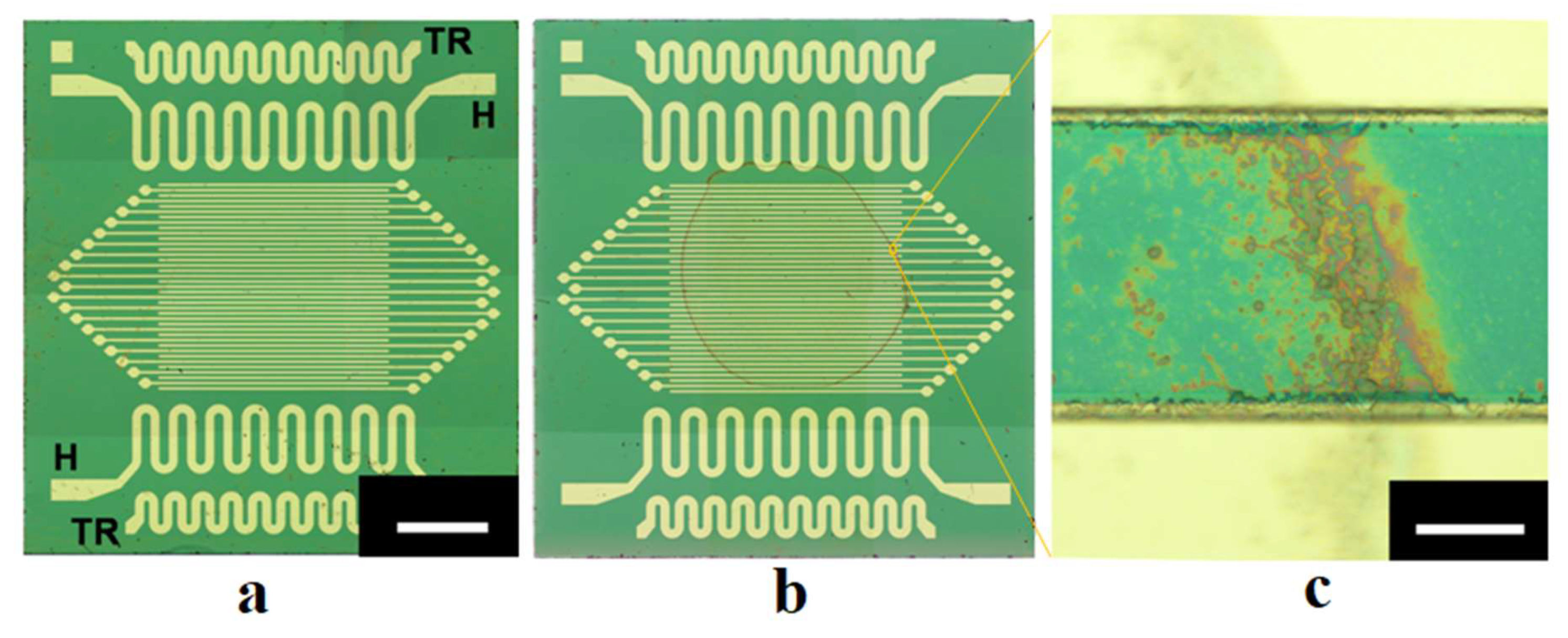
The studied stochastic structures of aggregated anatase particles were formed by “seeding” nanoparticles onto the surfaces of specially prepared silica substrates with flat interdigital electrode systems within the working zones overlapped by electrodes. These platinum interdigital electrode systems were produced on the surfaces of silica plates with the sizes of 9.0×10.0 mm2 and thickness of 0.3 mm using PVD technology (see Figure 1, a as an example of the substrate design). To expand the functionality of the substrates, they also contained flat resistive heaters and flat thermoresistors (respectively, positions H and TR in Figure 1, a). Two types of interdigital electrode systems with the following geometrical parameters were used:
1)
with an inter-electrode distance of (103.8±3.9) µm and electrode width of (89.8±5.7) µm;
2)
with the inter-electrode distance of (44.9±4.0) µm and electrode width of (54.2±5.2) µm.
In both cases, the number of electrode pairs was equal to 19; the sizes of the working zones defined by electrode-covered areas were 4.29×7.37 mm2 in the first case and 4.26×3.84 mm2 in the second case. The heights of electrodes above the surfaces of the substrates, measured using the Dektak 150 profilometer (the product of Veeco, USA), were approximately (0.88±0.02) µm in the first case and (1.61± 0.01) µm in the second case. Before electrical measurements, the contact pads of even and odd electrodes on the sides of the substrates were interconnected by jumpers and led out to connect them with the measuring units.
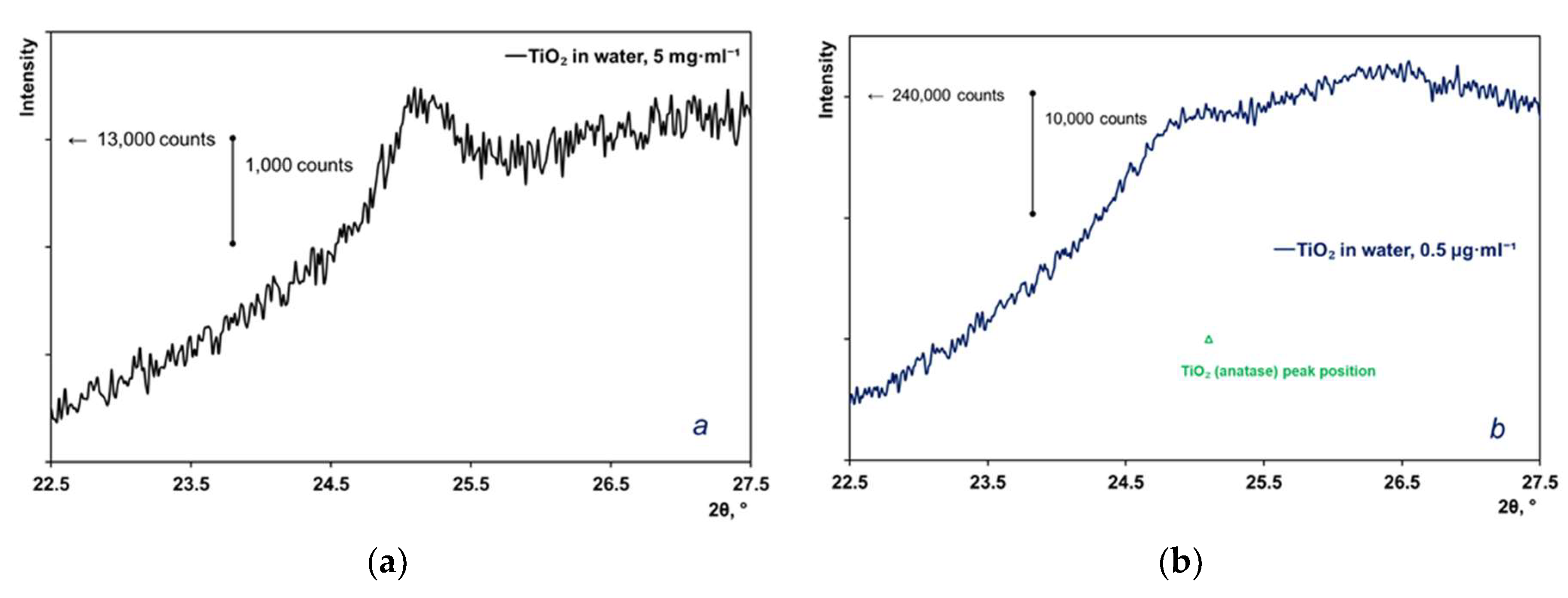
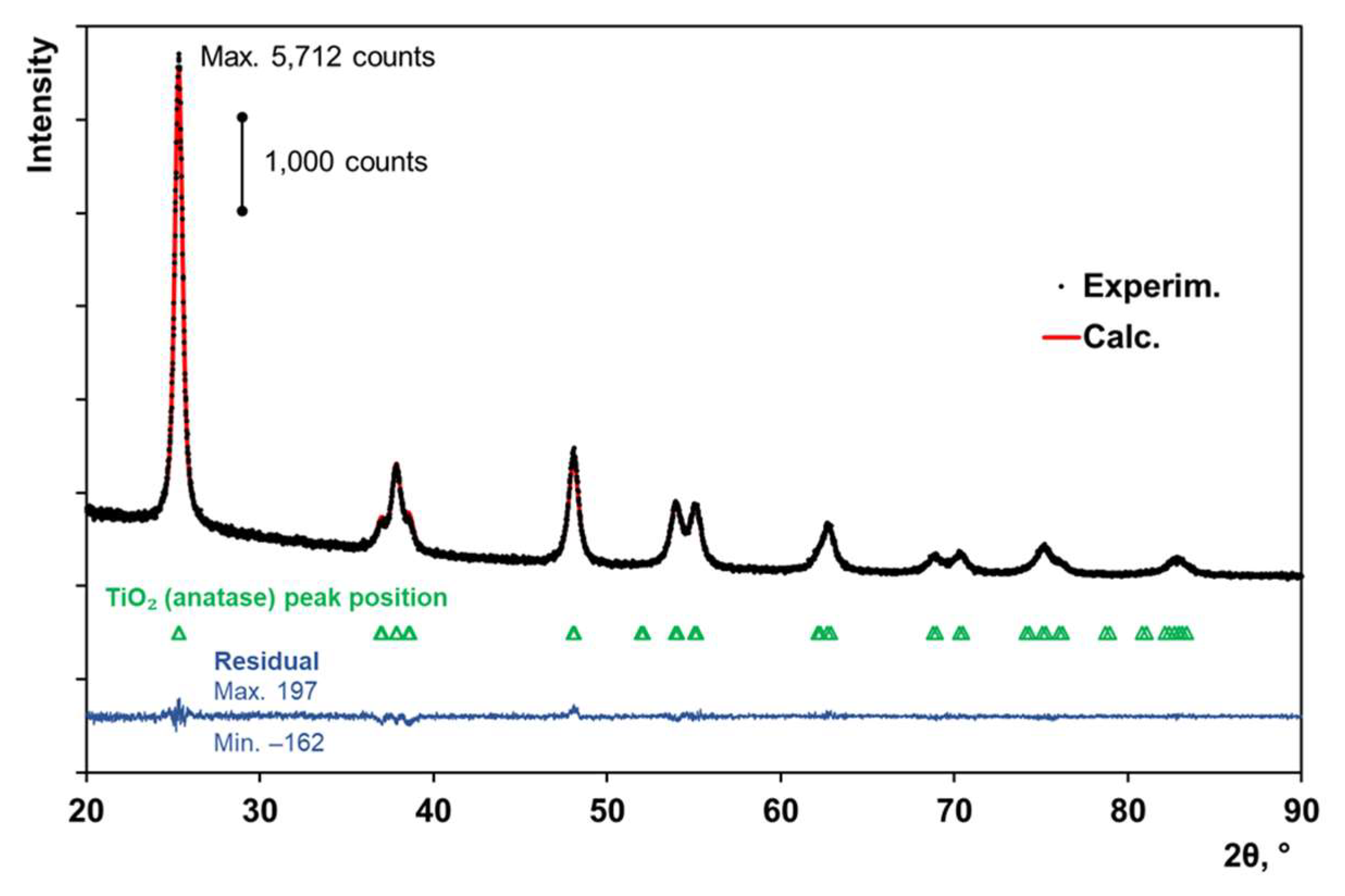
“Seeding” of TiO2 anatase nanoparticles onto the surfaces of substrates was carried out by applying small volumes of aqueous suspensions of particles to preliminarily cleaned substrate surfaces, followed by slow evaporation of water from the surfaces. The product #637254 of Sigma Aldrich Inc., USA (powder of polydisperse anatase nanoparticles with the average size ≤ 25 nm) was applied as the basic component of the prepared suspensions. Before preparing suspensions, the anatase powder was inspected using the X-ray diffractometry (DRON-8T X-ray diffractometer, the product of Bourevestnik, JSC, Russia) and the PDF-2 database (ICDD, USA). To record diffraction patterns, we used CuKα radiation, the Goebel parabolic mirror (AXO Dresden GmbH, Germany) and the Mythen 2R1D position-sensitive detector (Dectris, Switzerland). Figure 2 displays the X-ray diffractogram for the examined powder sample, and the design curve according to the full profile analysis. Based on the results of the full profile analysis (FullProf Suite), the anatase phase is characterized by the parameters of the tetragonal unit cell: a = (3.78608 ± 0.00009) Å and c = (9.50642 ± 0.00025) Å. For comparison, the database values (PDF no. 00-021-1272) are equal to 3.7852 Å and 9.5139 Å, respectively. Note that the average size of crystallites in the powder estimated using the Williamson-Hall technique [18,19] (≈ (23 ± 2) nm) fairly agrees with the upper level of the average size specified by the producer. Crystallinity of anatase nanoparticles is retained in a dilute aqueous suspension, which is confirmed by the presence of a peak in the X-ray diffraction pattern of this suspension (Figure 3). Thus, the "seeded" TiO2 nanoparticles are also crystalline.
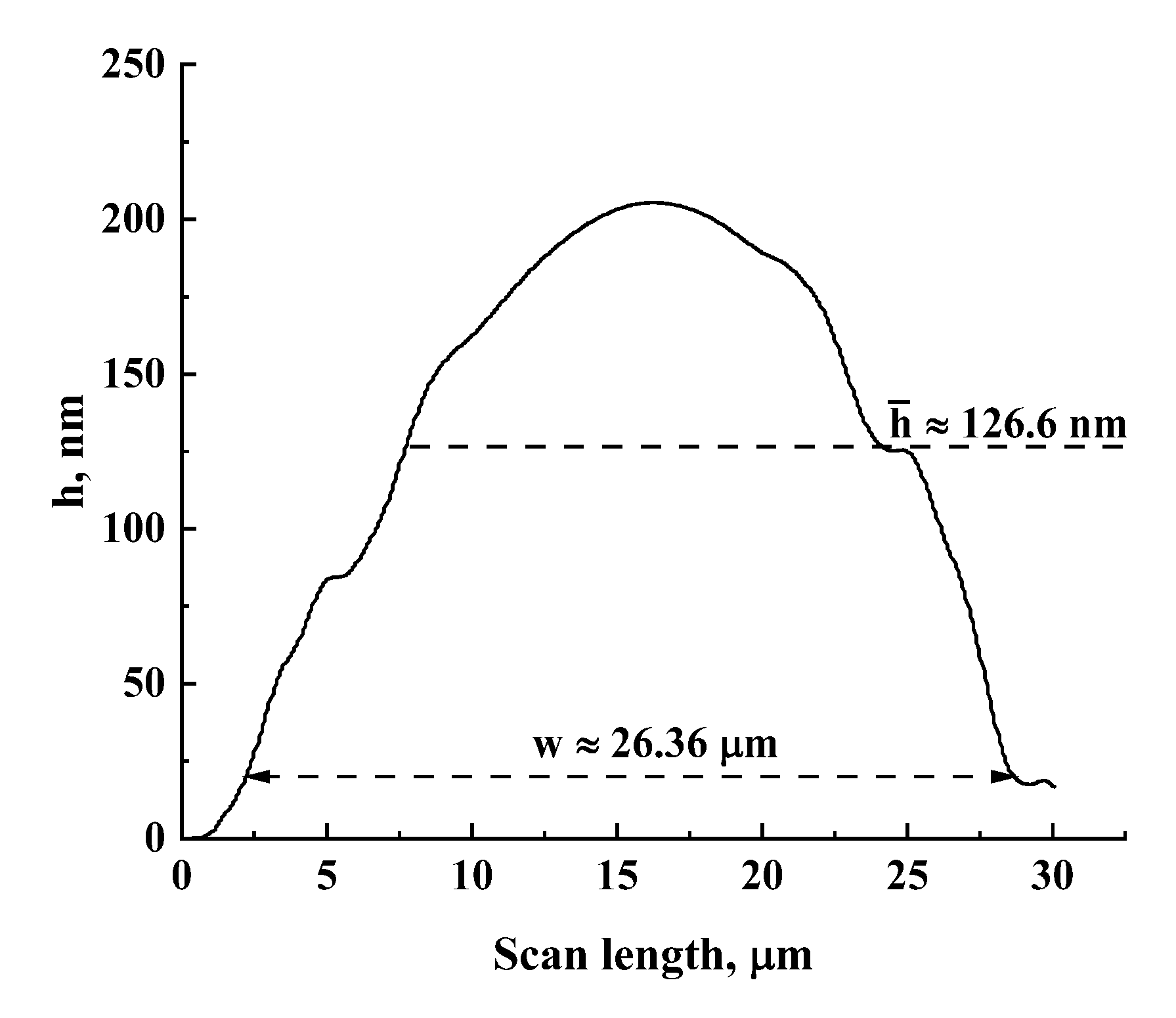
Suspensions were prepared using deionized water with the mass fractions of particles varied from 0.2 μg/ml to 0.5 μg/ml. The volume of suspensions applied to the surface of the substrates was equal to 8 μl. Note that in the case of an ideal uniform distribution of the sown particles across the working areas of 4.26×3.84 mm2, the mass fraction of 0.2 μg/ml corresponds to a particle layer with the thickness of ≈ 25 nm. In practice, formation of examined structures is governed by a variety of stochastic processes at the mesoscopic level, including local inhomogeneities in evaporation rates and capillary forces. Accordingly, long-term evaporation of water (approximately with 2-hour duration) from the suspension layers at room temperature led to formation of random distributions of single and aggregated nanoparticles across the working areas with a dominating occurrence of aggregated particles along initial borders of the applied drops of suspensions (Figure 1, b). Part of aggregated particles formed conductive bridges between adjacent electrodes, which can be identified by microscopic inspection of the surface of the fabricated samples (Figure 1, c). The number of these bridges providing initial conductivity of the studied samples of the order of 10-9 ÷ 10-8 S was approximately from 50 to 300 with an average width from 15 to 45 micrometers (depending on the mass fraction of particles in the applied drops). The heights of the bridges above the substrate surfaces were several dozens of nanometers; five arbitrarily chosen bridges were traced using the Dektak 150 profilometer at the minimal value of the stylus force (3 mg). Figure 4 displays a typical smoothed profilogram for one of the examined items. Based on the analysis of obtained smoothed profilograms, it was found that the following approximating relationship between the width
and average height h ¯ of bridges (see Figure 4) can be used with acceptable accuracy: h ¯ K b w , where K b (4.80 ± 0.32)⋅10-3.
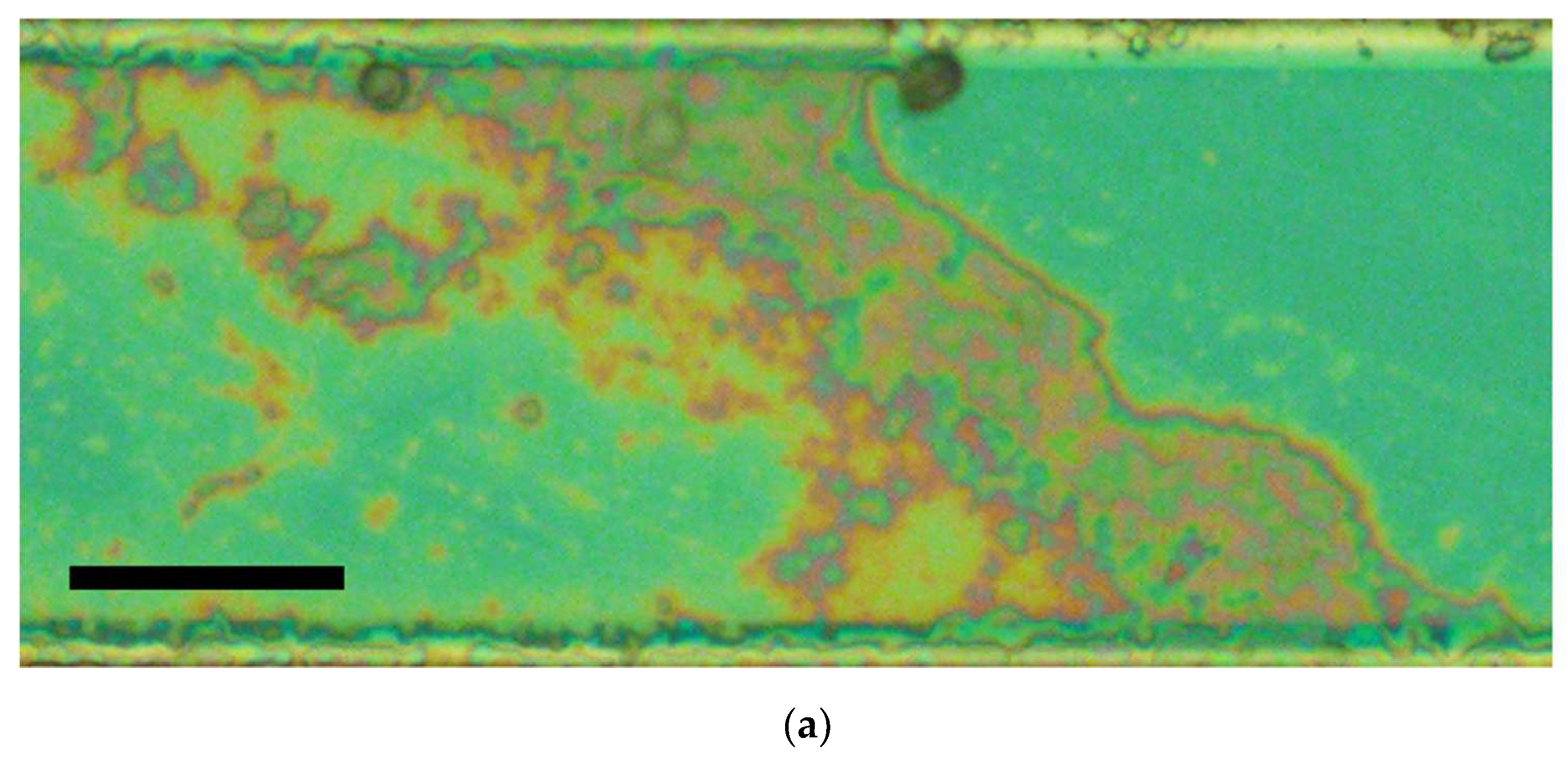
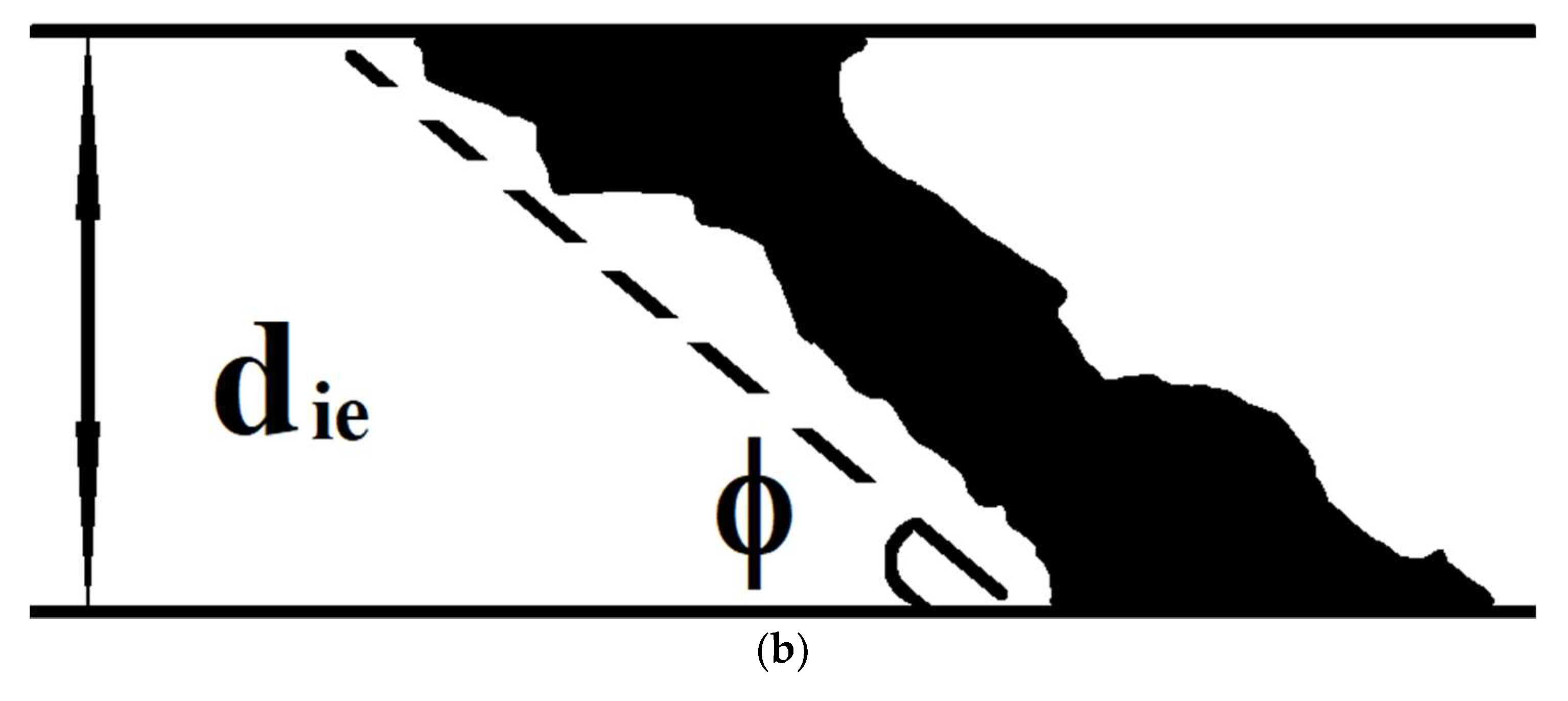
Due to stochasticity and, accordingly, uncontrollable formation of sets of interelectrode bridges in the “seeding” process, all the produced samples were subjected to thorough microscopic inspection before measuring their conductive properties. In the course of inspection, processing of the fragments of microscopic images with the interelectrode bridges was carried out in the following way (Figure 5): the processed fragment (a) was converted to a black-and-white format (b). Conversion was carried out in the interactive mode using manual tracing of the bridge boundaries and follow-up automatic filling of the area between the traced boundaries by black pixels. When tracing the bridge boundaries, adjacent island structures, and narrow and long branches oriented mainly across the interelectrode electric field were excluded (see Figure 5, b). These fragments should not have significant effect on the transfer of charge carriers through the bridges. After this, the bridge width was estimated as w N b p S p sin ϕ / d i e , where N b p is the number of automatically counted back pixels, S p is the area covered by a single pixel in the image, d i e is the inter-electrode distance, and ϕ is the inclination angle of the bridge with respect to electrodes (Figure 5, b).
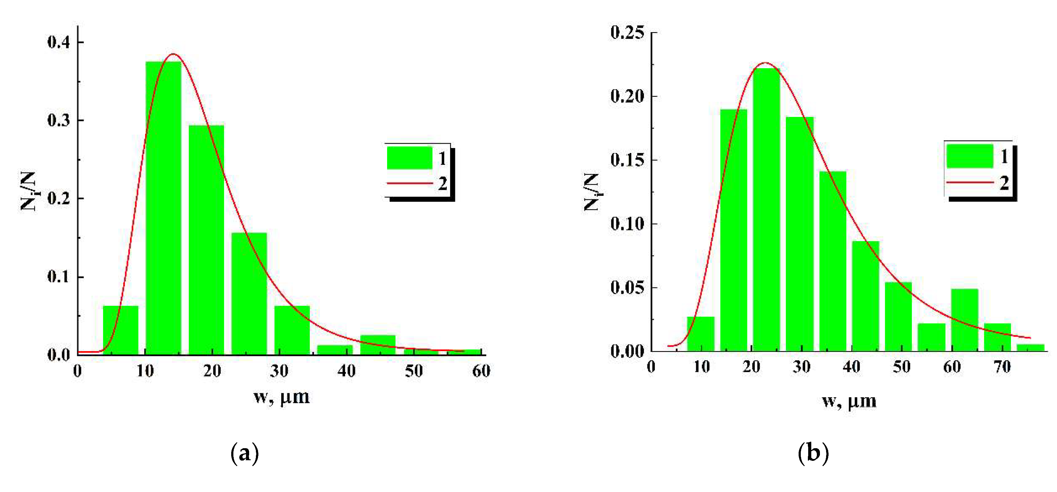
As the result of inspection, the sets of width values { w i } were obtained for all the produced samples. Statistical analysis of these datasets showed that sample probability density functions of w values with acceptable accuracy allow approximation by the lognormal distribution:
ρ ( w ) = ρ 0 + 1 2 π w σ w exp ( ( ln { w / w c } ) 2 2 σ w 2 ) ,
where σ w and w c are distribution parameters ( w = w c exp ( σ w 2 / 2 ) ), and ρ 0 is the offset occurring in the approximation. Figure 6 presents examples of histograms of w values along with approximating lognormal distributions for 2 samples with significantly differing average widths w of interelectrode bridges. In further study, the values of w and the number N b of the bridges connecting adjacent electrodes specified each examined sample.

2.2. Sample Examination

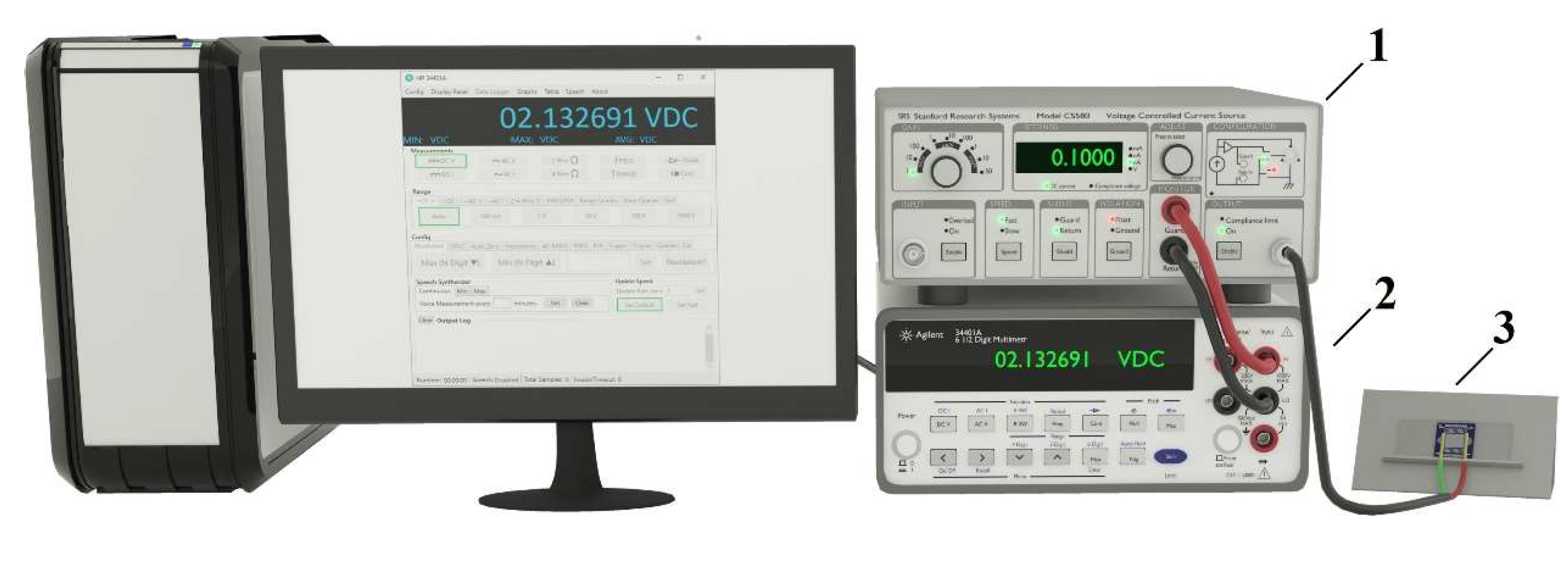
During the main experiments, time-dependent values of the ohmic conductivity G in the fabricated samples were studied in the direct current mode with the constant current of 1.0⋅10-9 A. Accordingly, instantaneous values of the voltage drop across the samples were acquired along the increasing time lapses; Figure 7 displays the corresponding experimental arrangement.
The voltage-controlled current source SRS CS-580 from the Stanford Research Systems (item 1) was applied to provide the established direct current in the examined samples. Instantaneous values of the voltage drop U ( t ) across the sample (item 3) were recorded using the data acquisition system based on the multimeter Agilent 34401A (item 2) controlled by PC. The sampling frequency was set equal to 20 Hz, and each recording run continued until the voltage drop across the examined sample reached 20 V. When this voltage threshold was overcome, the current source switched to the voltage stabilization mode and the data recording run was stopped. This limiting value was chosen to exclude possible electrical breakdowns of interelectrode gaps with a further increase in the voltage drop. Some of the samples were subjected to multiple (up to 6 times) sequential runs with 90-minute intervals between them. The purpose of such repeated experiments with the same samples was to evaluate the recovery rate for their conductivity, which dramatically fell down after completion of the first runs. The experiments were carried out at room temperature (25°С).
During the experiments, capacitance of the substrates with electrode systems and produced samples was measured before formation of ensembles of interelectrode bridges ( C s u b s t r a t e ), before the start of the first runs ( C s a m p l e ), and after their completion ( C s a m p l e ). In addition, capacitance of the connecting cables (the parasitic capacitance, C p a r ) was measured; measurements were provided using a multimeter unit (Keithley DAQ6510 type) with an error no worse than ± 1.0 pF. Additional measurements of these capacitance values using the Novocontrol Alpha AN impedance measuring system (Novocontrol Technologies GmbH & Co. KG, Montabaur, Germany) in the frequency range from 0.01 Hz to 105 Hz are in good agreement with the results obtained with the Keithley DAQ6510 multimeter.
Typically, the C s u b s t r a t e value for the first type of substrates is ≈ (490 ± 5) pF; the substrates of the second type (with interelectrode gaps of ≈ 44.9 µm) are characterized by the capacitance of (215 ± 3) pF. Formation of ensembles of interelectrode bridges causes small but systematic increase in the capacitance of the examined samples ( C s a m p l e C s u b s t r a t e (5 ÷ 7) pF, depending on the number and average width of the formed bridges). After the first runs, the differences C s a m p l e C s u b s t r a t e decrease with respect to C s a m p l e C s u b s t r a t e down to the values of the order (2 ÷ 3) pF. The reason for this behavior is considered in the “Discussion” section. Accordingly, these insignificant changes in the capacitance of the samples allow us to assume that C s a m p l e c o n s t in the course of the first and subsequent runs.
The measured parasitic capacitance was approximately equal to ≈ 180 pF; in combination with C s a m p l e , this value was used to obtain the total capacitance C t o t = C s a m p l e + C p a r necessary for recovery of the current values of the total ohmic conductivity G for the ensembles of interelectrode bridges.

3. Results

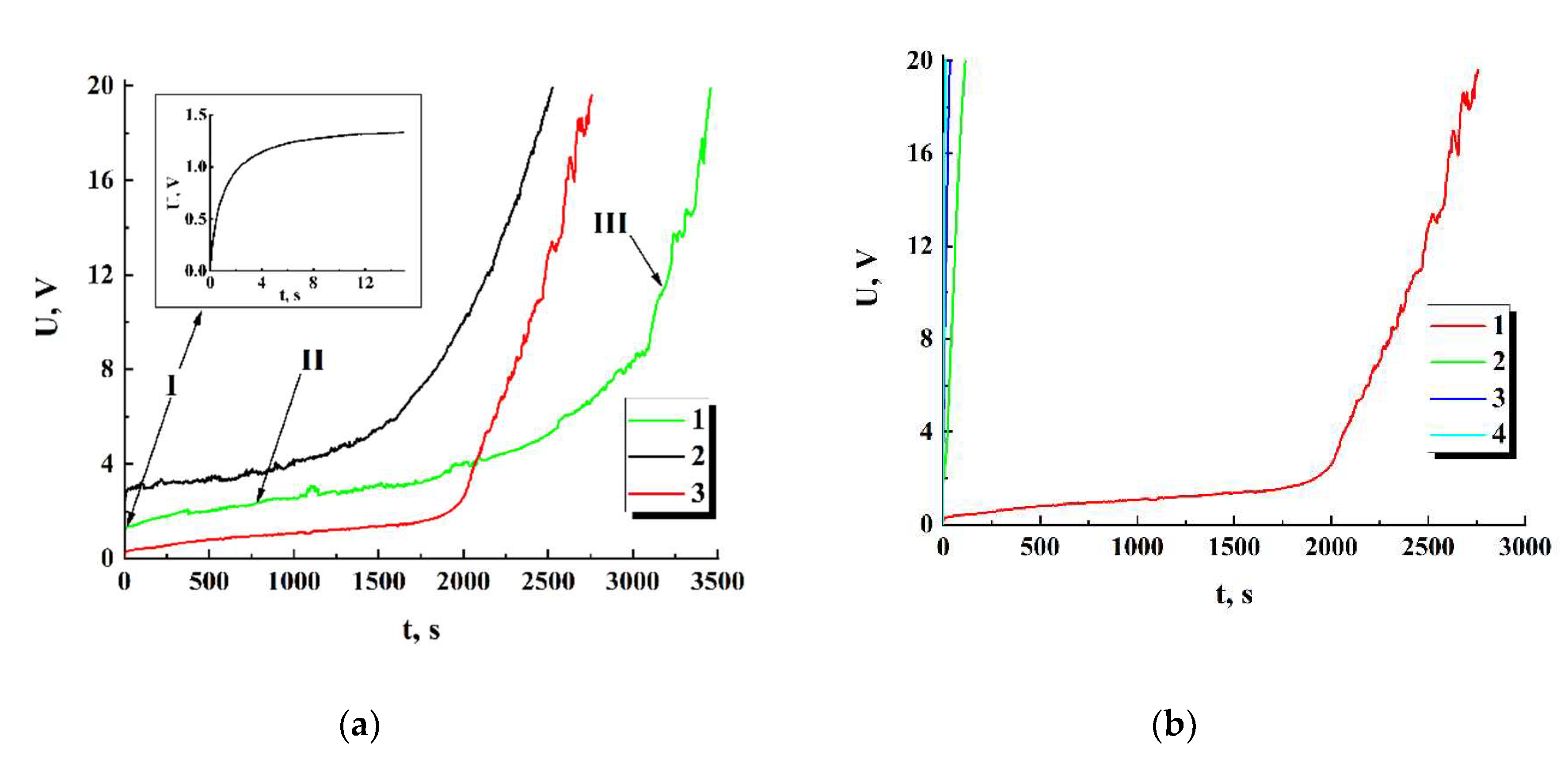
Figure 8, a illustrates typical behavior of the voltage drops across the examined samples with various values of w and N b during the first runs. Dependences U ( t ) can be divided into three characteristic regions: a short-term transitional region with duration of the order of several seconds (I); a quasi-stationary region, characterized by a slow increase in the voltage drop (II); and a region of rapid increase in U ( t ) (III). Duration of the quasi-stationary region II abruptly increases with an increase in the number of interelectrode bridges N b in the sample. In particular, pilot experiments with the samples fabricated with high mass fractions of nanoparticles in the applied suspensions (of the order of 0.7 µg/ml or more) and, correspondingly, characterized by large values of N b (of the order of 300 or more), showed absence of the “II → III” transition at the run times of the order of 6 hours or more. It can be assumed that this feature is due to existence of a certain critical value for the average current I / N b through the interelectrode bridges. When this critical value is exceeded in the ensemble of the bridges, a rather rapid degradation of their conducting structure occurs and, as a result, the “II → III” transition takes place within a foreseeable time.
Figure 8, b displays a typical set of U ( t ) dependences obtained in the experiment with the same sample subjected to a series of sequential runs with 90-minute intervals between them. It should be taken into account that in the case of direct current through the sample, a linear increase in the voltage drop U ( t ) t corresponds to its dominant capacitive susceptance. On the contrary, the case of U ( t ) c o n s t indicates the prevailing ohmic conductance in the sample. Accordingly, the data set shown in Figure 8, b indicates a catastrophic depletion of ensembles of free charge carriers in the interelectrode bridges in sequences of runs with low efficiency of restoring their concentration between runs.
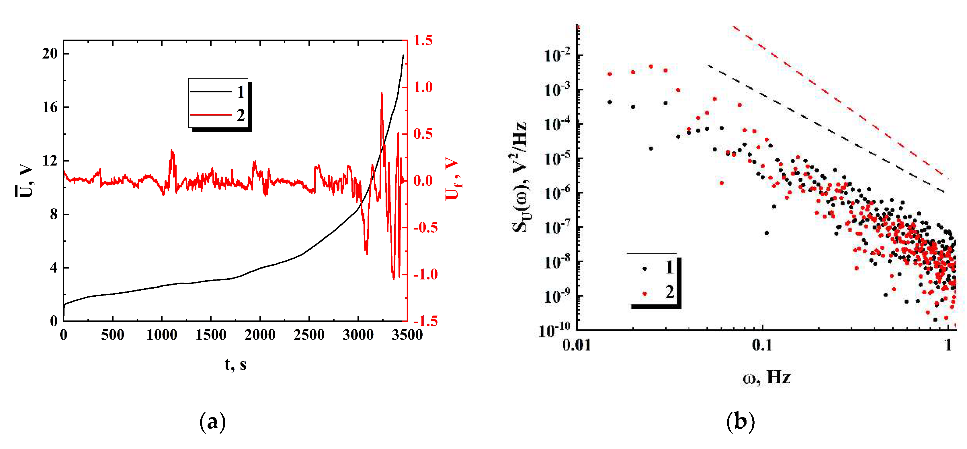
The dependencies U ( t ) obtained along the first runs were pre-processed to separate them into the trend ( U ¯ ( t ) ) and fluctuation ( U f ( t ) ) components using the adjacent averaging procedure; a running window with the width of 100 s was applied. As an example, Figure 9, a displays the result of this preprocessing for sample 3 (see Figure 8). Consideration of the sampled power spectra of fluctuation components calculated for 100-second sampling intervals within regions II and III showed that they allow the power-law approximation S U f ( ω ) ω γ with acceptable accuracy in the frequency intervals of 0.01 Hz ÷ 1 Hz (Figure 9, b). A remarkable feature is that, despite significant differences in the sampled power values U f 2 ( t ) ¯ of fluctuation components for various samples at stages II and III, the values of the spectral exponents γ for all samples exhibit a general tendency to increase from the values of the order of (2.6 ÷ 3.1) to the values of (3.5 ÷ 4.0) in the “II – III” transition. The reason for this behavior is considered in the “Discussion” section.

4. Discussion

4.1. Recovery of Time-Dependent Smoothed Conductivity in the Examined Samples

The basic relationship describing the voltage response U ( t ) of the examined samples under affect of the constant direct current I can be written in the following form:
I = G ( t ) U ( t ) + C t o t d U ( t ) d t .
Here we neglect small variations of the total capacitance of the system “sample + connecting cables” along the runs. Considering the trend components U ¯ ( t ) of the “voltage drop – time lapse” dependencies, we arrive to the following expression for evaluation of the smoothed time-dependent conductivity:
G ¯ ( t ) = I C t o t ( d U ¯ ( t ) / d t ) U ¯ ( t ) .
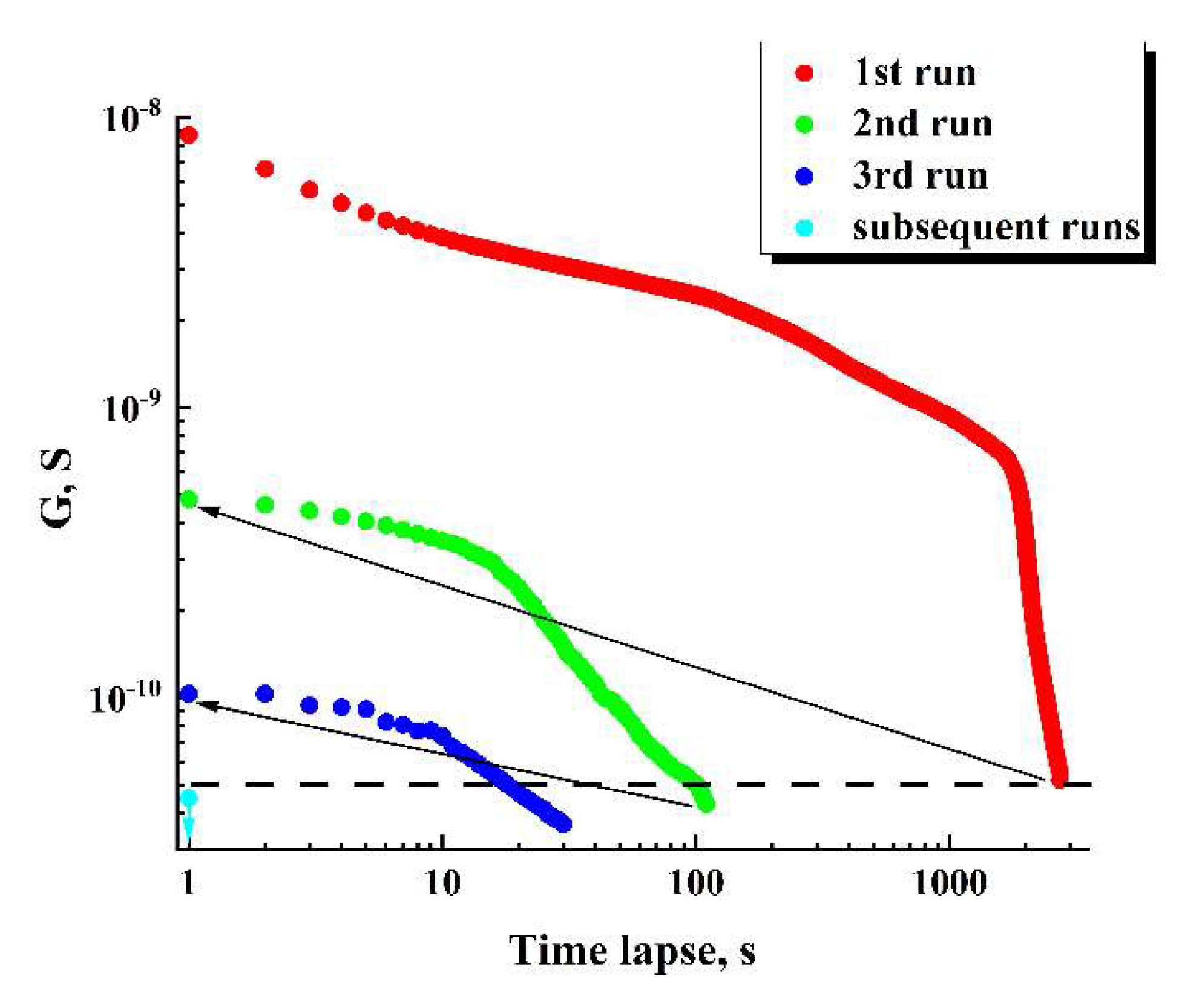
In this case, the term "smoothed conductivity" means evaluation of G at the moment using the corresponding values of the voltage and its first derivative estimated for the trend component U ¯ ( t ) . As an example, Figure 10 displays the values of G ¯ against the time lapse recovered for the series of sequential runs (for the initial datasets see Figure 8, b). The recovered dataset G ¯ ( t ) for the first run exhibits the behavior at the final stage of the run, which is typical for percolation systems near the threshold.
The horizontal dashed line corresponds to the minimal value of “pure” ohmic conductivity (5⋅10-11 S) achieved under U ¯ ( t ) = 20 V in the case of C t o t ( d U ¯ ( t ) / d t ) = 0. During the first runs, the achievable maximal values of the displacement current in the samples are many times less than the set value of the total current (1 nA). On subsequent runs, contribution of the displacement current to the total current gradually becomes dominant. Accordingly, the recovered G ¯ values are below the dotted threshold line on the graph.
The arrows indicate partial recovery of ohmic conductivity in the examined sample during 90-minute time intervals between the first-second and second-third runs. However, it should be noted that this recovery under the used conditions (in particular, at room temperature) is subtle and decreases from run to run. In the subsequent runs, ohmic conductivity occurs vanishingly small (the single cyan marker).

4.2. Scaling Behavior of G ¯

and the Conductivity Critical Exponent
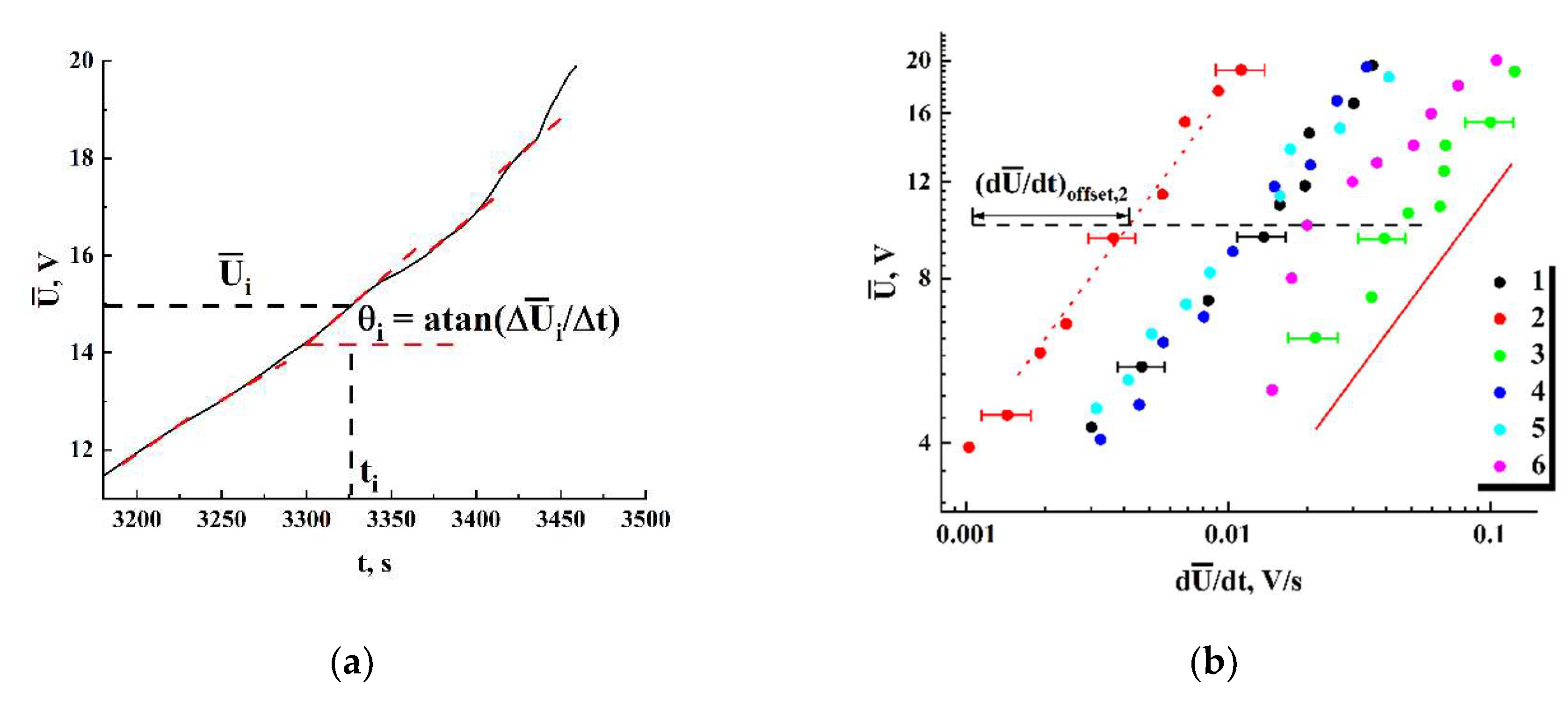
At the final stages of the first runs, when conducting systems in the studied samples approach their critical states, contributions of the displacement current C t o t ( d U ¯ ( t ) / d t ) to the total current are small and the trend components of U ( t ) are mainly governed by G ¯ ( t ) : U ¯ ( t ) I / G ¯ ( t ) . On the other hand, the general property of percolation systems is power-law dependence of the system conductivity on detuning the governing parameter p ( t ) from its critical value p c : G ¯ ( t ) [ Δ p ( t ) ] α , where Δ p ( t ) = [ p c p ( t ) ] / p c . For the examined systems, which consist of large sets of statistically independent random conduction channels (percolation clusters), the control parameter p ( t ) is associated, for example, with the number of blocked nodes or bonds in these percolation clusters. Accordingly, when Δ p ( t ) 0 , G ¯ ( t ) falls down ( α should have a positive value). The trend component of the voltage drop U ¯ ( t ) should exhibit a similar behavior near the threshold of ohmic conductance: U ¯ ( t ) [ Δ p ( t ) ] β ( β = α is negative). The first derivative d U ¯ ( t ) / d t can be expressed as d U ¯ ( t ) / d t [ Δ p ( t ) ] β 1 [ d { Δ p ( t ) } / d t ] . This expression can be rewritten in the following form: d U ¯ ( t ) / d t [ U ¯ ( t ) ] β 1 β [ d { Δ p ( t ) } / d t ] . We can assume that, at a rather short stage of rapid growth in U ¯ ( t ) , the dependence p ( t ) admits a linear approximation ( p ( t ) t and, accordingly, d { Δ p ( t ) } / d t c o n s t = K p . Under these assumptions, we arrive to the following reduced relationship between the current values of U ¯ ( t ) and corresponding first derivatives:
U ¯ ( t ) d t [ U ¯ ( t ) ] β 1 β K p .
Figure 11, a illustrates the procedure for estimating U ¯ and d U ¯ / d t values from the obtained trend curves U ¯ ( t ) . Figure 10, b displays in the logarithmic coordinates the sets of pairs ( d U ¯ / d t , U ¯ ) corresponding to the final stages of the fist runs for various examined samples. Note that, despite a remarkable scattering of these datasets across the ( d U ¯ / d t , U ¯ ) coordinate plane, they exhibit common power-law trends with the close values of slopes in logarithmic coordinates. The red dashed line with the slope of ≈ 0.615 ± 0.029 indicates this common trend for all the datasets and serves as a guide for the eye. Selectively shown error bars for the values of d U ¯ / d t correspond to the confidence level of 0.9. Note that for this data presentation scheme ( d U ¯ / d t is an argument, and U ¯ is a function), the slope of the trend line is determined by the ratio β / ( β 1 ) ; thus, the critical exponent for the trend value of the voltage drop is estimated as ≈ -1.597.
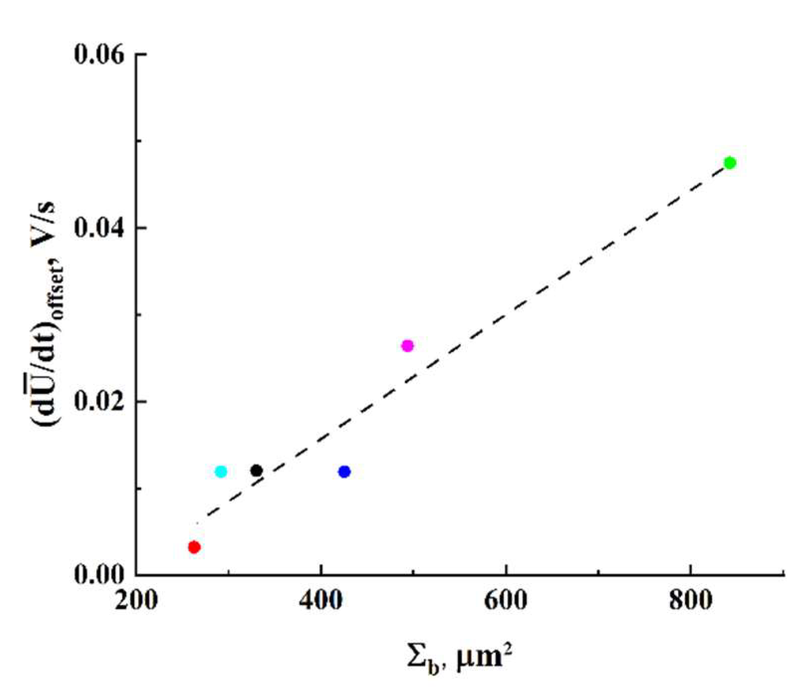
According to Eq. 4, mutual shifts of the datasets in the coordinate plane can be due to different values of the parameter K p for these samples. As follows from the above consideration, this parameter characterizes the rate in the increase of the number of blocked nodes or bonds in the model percolation system that mimics the studied ensembles of interelectrode conductive bridges. Larger values of K p should lead to larger values of the first derivative d U ¯ / d t for the same values of U ¯ . Note that there is a certain correlation between the shifts of the datasets towards large values of d U ¯ / d t and N b , w b values characterizing the studied samples. The parameter Σ b = K b w 2 N b can be considered as a measure of the total cross-section of interelectrode bridges in the sample. Accordingly, the average current density in the examined samples is proportional to the ratio I / Σ b . Figure 11 displays the dataset shifts ( d U ¯ / d t ) o f f s e t along the d U ¯ / d t axis (Figure 10) against Σ b ; the shifts were estimated with respect to the reference point ( d U ¯ / d t = 1.0⋅10-3 V/s; V ¯ = 10 V, see Figure 11, b). The values of ( d U ¯ / d t ) o f f s e t are associated with the introduced rate parameter K p up to a constant factor (see Eq. 4); thus, it can be concluded that lower average current densities in the samples at stage III cause larger rates of their approach to the percolation threshold. This conclusion may seem rather trivial, but the established features of the influence of geometry of systems, described in terms of the parameter Σ b , on the decay of ohmic conductivity can be useful for a deeper understanding of the behavior of such systems near the percolation threshold. In particular, one of these features is a close-to-linear relationship between Σ b and K p (Figure 12).
It is interesting to compare the obtained value of the critical exponent for ohmic conductivity with a variety of currently known similar values, obtained mainly using statistical modeling or other theoretical approaches. Numerous theoretical studies of percolation in 3D resistive grids carried out since the nineties of the last century gave the value of the critical conductivity exponent close to 2.0 (see, e.g. [20,21,22]). These values significantly exceed the value established in accordance with the method under discussion. On the other hand, modeling of percolation in two-dimensional lattices leads to the values of the critical conductivity exponent of the order of 1.3 (see, e.g., [23,24]). When comparing the value obtained from our experimental results and the critical exponents obtained for the model 3D and 2D percolation systems, it must be taken into account that the conducting structures (interelectrode bridges) studied in our case are rather transitional between two-dimensional and three-dimensional conducting systems (the form factor K b is very small). It should also be noted that a rigorous theoretical analysis of the "conductor-insulator" transition using the transfer matrix approach was carried out in [25], gave a value of the critical conductivity exponent of the order of 1.54 ± 0.08, which is fairly close to our result.

4.3. Comments on DC Conductivity and Permittivity of the Studied Systems

We consider the following qualitative model of conductivity evolution in the ensembles of interelectrode bridges under the influence of direct current:
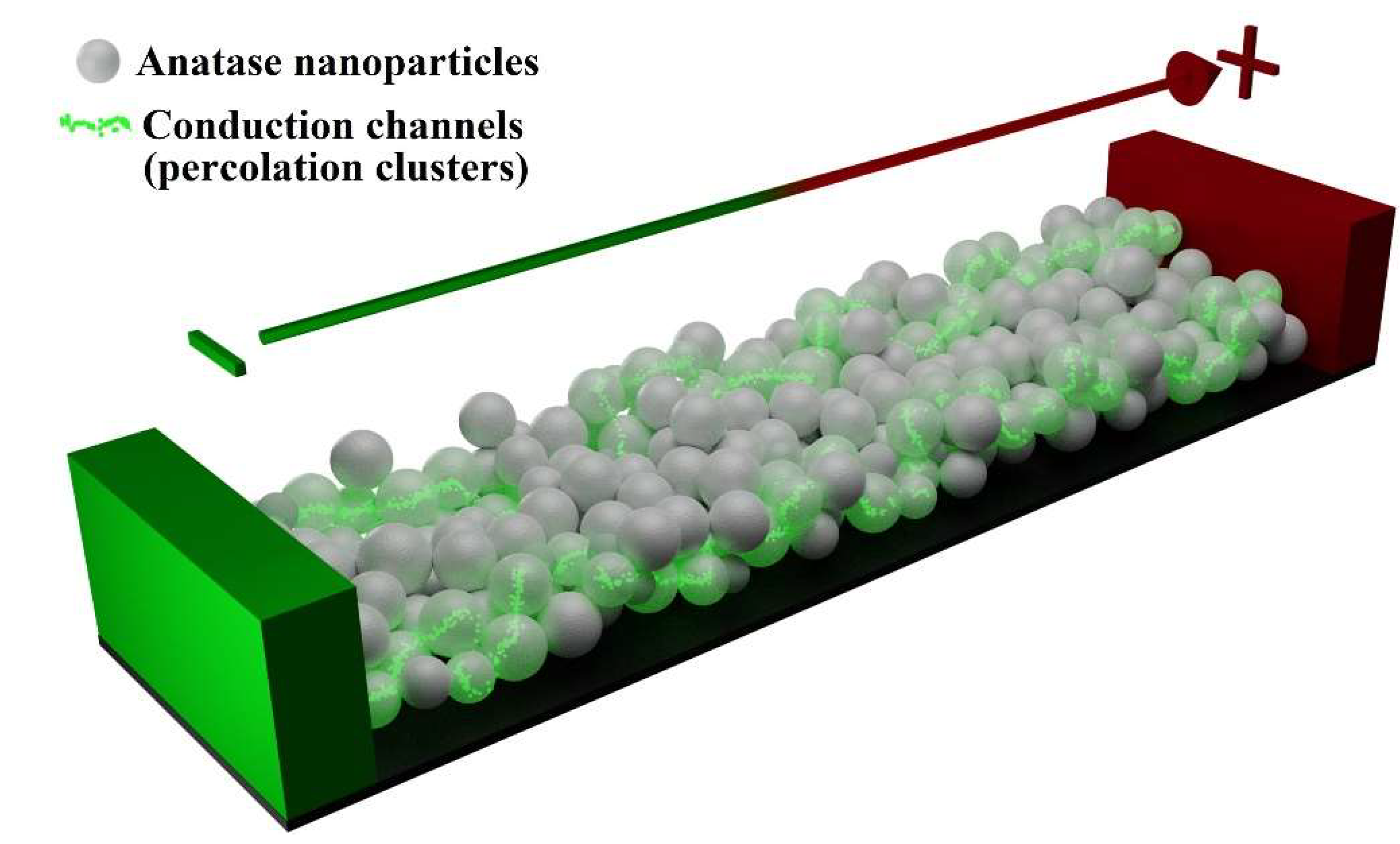
1) during a short-term stage I (see inset in Figure 8, a), sets of conduction channels (percolation clusters) are formed in the interelectrode bridges (Figure 13);
2) a long-term quasi-stationary stage II is characterized by a gradual decrease in ohmic conductivity of the bridges (see the dataset 1 in Figure 10) due to decrease in the number of conduction channels previously formed at a stage I; this effect can be considered in terms of accumulating decrease in the concentration of electrons due to their capture by deep traps in anatase nanoparticles during electron transport in the bridges;
3) as the number of conduction channels in the bridges approaches a critical value corresponding to the percolation threshold, a rapid decrease in ohmic conductivity and, accordingly, an abrupt increase in voltage drops across the studied samples occurs (stage III).
It can be assumed that the characteristic formation time t f for the sets of conduction channels in the bridges at stage I should correlate with the characteristic time of electron transfer through the bridges. This assumption makes it possible to roughly estimate the electron mobility μ e in the studied structures of close-packed anatase nanoparticles.
Accordingly, we can write the following approximate expression for the relationship between t f and the interelectrode distance d i e :
d i e μ e d i e 0 t f U ( t ) d t .
As t f , we take the time interval when the derivative d U ( t ) / d t at stage I decreases (see inset in Figure 8, a) to a level of 0.05 from the initial value. Thus, electron mobility in the studied structures can be roughly estimated as:
μ e d i e 2 0 t f U ( t ) d t .
Analysis of initial fragments of U ( t ) dependencies (stage I) for a group of 5 samples with various N b and w b but the same interelectrode distance d i e ≈ 44.9 µm gave a range of 0 t f U ( t ) d t as ≈ (6.18 ± 3.69) V⋅s. Accordingly, μ e for the studied samples was roughly estimated as ≈ (3.72 ± 2.16)⋅10-6 cm2/V⋅s. It should be noted that this estimation approach is simplified and does not take into account a variety of influencing factors (e.g., non-uniformity of the electric field in the interelectrode space, and so on). Therefore, strictly speaking, its applicability is limited to estimates of the order of magnitude. Nevertheless, the obtained value of the electron mobility satisfactorily agrees with the value μ e ≈ 5.0⋅10-6 cm2/V⋅s for nanoporous anatase, obtained using the measurements of the photoresponse under laser irradiation and presented in [26]. The specimens studied in this work were obtained by annealing a mixture of 16-nm particles of anatase and turpentine oil on glass substrates and were characterized by the anatase volume fraction of about 50%.
Based on the obtained approximate value of μ e and typical voltage drops U b at the beginning of a quasi-stationary stage II (Figure 8, a), we can roughly estimate the initial concentration n e of conduction electrons in the formed bridge-like structures. Depending on N b and w , these voltage drops for the samples of the second group range from 1 to 3 V. The value of n e can be expressed as n e I d i e / ( N b K b w 2 e μ e U b ) , where e is the electron charge. Accordingly, n e (1.31 ± 0.52)⋅1018 cm-3. Taking into account the factor ψ of filling the volume of bridge-like structures with nanoparticles, we can estimate electron concentration in the nanophase. The approximate value ψ 0.45 was obtained on the basis of volumetric estimations and measurements of N b and w . As a result, we arrive to the following estimate for the anatase nanophase: n e , n p h = n e / ψ (2.92 ± 1.15)⋅1018 cm-3. This value can be compared to the published experimental data on the concentration of conduction electrons in the undoped anatase (see numerous references and corresponding Table 2 in [27]). It should be noted that, depending on the preparation technique, these data are strongly scattered in the range from ~1.0⋅1016 cm-3 to ~ 9⋅1019 cm-3, though, most results fall within the range of ≈ 3.2⋅1017 cm-3 to ≈ 2.0⋅1019 cm-3. Thus, the obtained value of n e , n p h seems quite reasonable.
It is interesting to estimate an average number of conduction electrons per one nanoparticle; in our case, this value occurs approximately equal to N ˜ c e 24. On the other hand, each nanoparticle is characterized by a certain number of deep traps capable of arresting conduction electrons. According to the photoconductivity data for the nanostructured anatase, the estimated number of traps N t r per one nanoparticle with the average diameter of 16 nm is of the order of 28 [28]; so a large value is reasonably explained by a great amount of surface states in anatase nanoparticles. In our case, the average number of traps per particle presumably exceeds this value due to a larger average surface of particles. It is obvious that the ratio between N t r and N ˜ c e has a crucial influence on degradation of ohmic conductivity in the process of electron transfer in the bridge-like structures. A detailed quantitative analysis of this influence is beyond the scope of this work and is the object of further study.
Consideration of a small but systematic increase in the capacitance of samples resulted from formation of ensembles of interelectrode bridges (see Section 2) makes it possible to estimate the real part of their initial effective permittivity ε e f . A rigorous quantitative analysis of the influence of ε e f on C s a m p l e is a complicated problem, which is far beyond the scope of this work. Therefore, we applied an approximate approach based on the assumption of a close-to-linear dependence of the capacitance increment C s a m p l e C s u b s t r a t e on the ratio of the area covered by the bridges ( S b ) to the total area covered by the electrodes ( S e ). Within this approach, the relative capacitance increment η = ( C s a m p l e C s u b s t r a t e ) / C s u b s t r a t e can be expressed as η ( ε e f 1 ) ( S b / S e ) ψ h . In this expression, the factor ψ h is equal to the ratio of the average height of the bridges to the height of electrodes and takes into account a partial filling of the interelectrode space along the height with the nanoparticles. For a confidence level of 0.9, the ratios ( S b / S e ) for the samples of the first group are in the range from 0.00524 to 0.01212, and the mean value is ≈ 0.0087. Similarly, the ψ h factor is characterized by the range from 0.0514 to 0.0801 and the mean value of 0.0658. With the average value of η approximately equal to 0.03, we obtained effective permittivity of the examined anatase bridges as ≈ 56.0 ± 17.4. Note that such high permittivity values for the anatase-based structures is not surprising. To verify the obtained data, low-frequency permittivity (in the range from 1 Hz to 103 Hz) of the layers of densely packed nanoparticles (the same product #637254 of Sigma Aldrich Inc. as applied for the sample preparation) was measured using the Novocontrol Alpha AN impedance measuring system. The layers were tightly pressed up to the values of the anatase volume fraction of the order of 0.7. The obtained value of the real part of low-frequency permittivity is approximately equal to 70. Applying the Maxwell Garnet model of an effective medium [29] and considering the anatase phase in the prepared layers as the matrix substance with air inclusions, we can recover permittivity of the bulk anatase as ≈ 115. Evaluation of effective permittivity for the substance of bridges with 0.45 volume fraction of anatase carried out using the Maxwell Garnet model gave ε e f 41. This estimate is remarkably less than the above presented mean value (≈ 56) resulted from the capacitance increment analysis. However, it should be noted that systematic errors of the Maxwell Garnet model rise up when the volume fractions of the matrix and inclusions are comparable and their permittivity values strongly differ from each other. In addition, taking into account an abundance of assumptions in the capacitance analysis, we can suggest a satisfactory agreement between these data.
It should be noted that the effect of an anomalous increase in the permittivity of percolation systems near the percolation threshold discussed in a number of works (see, e.g., [30,31,32]) was not observed in our experiments. On the contrary, at the end of the first runs, when ohmic conductivity of the examined samples decreases over short time intervals by two orders of magnitude or more (Figure 10, a), there is a significant (up to 2–3 times) decrease in η . Accordingly, effective permittivity of the interelectrode bridges falls down by the same number of times. This effect is a direct consequence of localization of a significant number of conduction electrons on the traps, which leads to a significant decrease in polarizability of nanoparticles and, accordingly, of the entire substance forming the bridges. A similar effect associated with localization of photoinduced electrons on the traps during a long-term laser action on anatase nanoparticles in the fundamental absorption band was discussed in [17].

4.4. Spectral Properties of the Noise of Conduction Current

Eq. 2 can be rewritten in the following form:
I = I c o n d ( t ) + C t o t d U ( t ) d t .
Here, I c o n d ( t ) is an instantaneous value of conduction current associated with a transfer of conduction electrons between the systems of electrodes of opposite signs. Differentiating Eq. 7 and considering spectral densities of the conduction current, the displacement current and their derivatives, and taking into account the relationships between them, we obtain:
ω 2 S I c o n d ( ω ) = C t o t 2 ω 4 S U ( ω ) .
Thus, the spectral density of conduction current fluctuations can be recovered from the spectral density of voltage drop fluctuations applying the renormalization factor C t o t 2 ω 2 . The power spectra of the voltage drop fluctuations S U ( ω ) typically exhibit a decay, which is close to the power law S U ( ω ) ω γ in the frequency range from 0.01 Hz to 1 Hz (see Figure 9, b). Accordingly, the spectral exponent of conduction current fluctuations γ = 2 γ is in the range of (-1.0 ÷ -0.5) at the quasi-stationary stage and decreases down to (-1.5 ÷ -2.0) at the final stages of the first runs. The behavior S I c o n d ( ω ) ω 1 is associated with a classical flicker noise observed in a variety of conducting systems. At the same time, a remarkably high noise level for the examined systems should be noted; the normalized root-mean-square values of conduction current fluctuations at the quasi-stationary stage are typically in the range from ≈ 5⋅10-3 to ≈ 1.2⋅10-2. This feature is presumably due to the quasi-stationary dynamics of ensembles of conducting channels in all bridges. Such dynamics manifests itself in the opening of new and blocking of some of the existing channels with minor changes in their total number.
A decrease in the spectral exponent γ of conduction current fluctuations down to the values close to -2 indicates emergence of a new mechanism that controls a transfer of mobile charge carriers at the stage of significant conductivity decay. Also, considering a significant increase in the root-mean-square values of U f ( t ) at this stage (Figure 9, a), it can be assumed appearance of avalanche breakdowns in groups of mutually connected previously blocked channels with a rapid increase in the voltage drop across the samples.
5. Conclusions

Thus, the observed features of electron transfer in the bridge-like disordered ensembles of anatase nanoparticles demonstrate the achievement of a percolation threshold upon the prolonged exposure to direct current and an extremely low rate of the degraded conductivity recovery after termination of the current action. These features can be interpreted as a manifestation of a "semiconductor-insulator" transition in such structures and are due to the depletion of ensembles of conduction electrons captured in the process of transfer through the structure by deep traps in anatase nanoparticles. This transition manifests itself in limited ranges of a number of bridges and their average width, which determine a total cross section of the conducting structure. The established value of the critical conductivity exponent for the studied structures has an intermediate value between theoretical values for three-dimensional and two-dimensional percolation systems. This circumstance seems reasonable, since the form factor of interelectrode bridges created during the experiment is quite small and, accordingly, the formed structures can be considered as transitional between two-dimensional and three-dimensional conducting systems.
For the examined samples, there are no manifestations of theoretically predicted and, in some cases, experimentally observed effect of significant increase in the system permittivity in the region of the "conductor-insulator" transition. On the contrary, according to our estimates, there is a systematic decrease in permittivity of the bridge material near the percolation threshold, due to localization of the main fraction of mobile carriers in the traps and, accordingly, a decrease in the system polarizability in the constant electric field.
A remarkable feature of conductivity fluctuations in the studied systems as they approach the percolation threshold is a decrease in the spectral exponent, which characterizes the power-law decay in the spectral density of fluctuations, to the values close to -2. This feature indicates an increasing influence of avalanche-like local charge transfers in the groups of previously blocked conduction channels on the integral charge transfer as the threshold is approached.
The authors believe that the presented results and the discussed techniques will be useful in the further design and characterization of dispersed partially conductive nanomaterials for electronic and sensor applications.

Author Contributions

Conceptualization, D.A.Z.; methodology, D.A.Z.; software, S.S.V, D.V.T, and D.A.V.; validation, S.S.V., I.A.P., M.Yu.V., and A.V.U.; formal analysis, D.A.Z., S.S.V., A.S.V., and N.V.G.; investigation, S.S.V., M.Yu.V., I.A.P., and A.S.T.; resources, M.Yu.V., A.S.V., and A.V.U.; data curation, S.S.V., A.S.T., N.V.G. and D.V.T.; writing—original draft preparation, D.A.Z., M.Yu.V., and A.V.U.; writing—review and editing, D.A.Z.; visualization, D.V.T. and D.A.V.; supervision, D.A.Z.; project administration, D.A.Z. and S.S.V.; funding acquisition, D.A.Z. All authors have read and agreed to the published version of the manuscript.

Funding

This research was funded by the Russian Science Foundation, grant number 22-29-00612.

Data Availability Statement

Raw data will be provided by the corresponding author upon request.

Acknowledgments

The authors are grateful to A.Kh. Askarova for literary editing of the manuscript.

Conflicts of Interest

The authors declare no conflict of interest.

References

  1. Witkiewicz, Z.; Jasek, K.; Grabka, M. Semiconductor gas sensors for detecting chemical warfare agents and their simulants. Sensors 2023, 23, 3272. [Google Scholar] [CrossRef] [PubMed]
  2. Qin, Q.; Olimov, D.; Yin, L. Semiconductor-type gas sensors based on γ-Fe2O3 nanoparticles and its derivatives in conjunction with SnO2 and graphene. Chemosensors 2022, 10, 267. [Google Scholar] [CrossRef]
  3. Sharma, A.; Ahmed, A.; Singh, A.; Oruganti, S.K.; Khosla, A.; Arya, S. Review - recent advances in tin oxide nanomaterials as electrochemical/chemiresistive sensors. Journal of the Electrochemical Society 2021, 168, 027505. [Google Scholar] [CrossRef]
  4. Chen, N.; Deng, D.; Li, Y.; Xing, X.; Liu, X.; Xiao, X.; Wang, Y. The xylene sensing performance of WO3 decorated anatase TiO2 nanoparticles as a sensing material for a gas sensor at a low operating temperature. RSC Advances 2016, 6, 49692–49701. [Google Scholar] [CrossRef]
  5. Feiyu, D.; Wang, Y. Transition metal oxide nanostructures: premeditated fabrication and applications in electronic and photonic devices. Journal of materials science 2018, 53, 4334–4359. [Google Scholar]
  6. Sudarshan, S.; Das, S.; Ray, S.K. Progress in group-IV semiconductor nanowires based photonic devices. Applied Physics A 2023, 129, 216. [Google Scholar]
  7. Baldini, E.; Palmieri, T.; Pomarico, E.; Auböck, G.; Chergui, M. Clocking the ultrafast electron cooling in anatase titanium dioxide nanoparticles. ACS Photonics 2018, 5, 1241–1249. [Google Scholar] [CrossRef]
  8. Song, Y.; You, K.; Chen, Y.; Zhao, J.; Jiang, X.; Ge, Y.; Wang, Y.; Zheng, J.; Xing, C.; Zhang, H. Lead monoxide: a promising two-dimensional layered material for applications in nonlinear photonics in the infrared band. Nanoscale 2019, 11, 12595. [Google Scholar] [CrossRef]
  9. Terna, A.D.; Elemike, E.E.; Mbonu, J.I.; Osafile, O.E.; Ezeani, R.O. The future of semiconductors nanoparticles: Synthesis, properties and applications. Materials Science & Engineering B 2021, 272, 115363. [Google Scholar]
  10. Collins, G.; Lonergan, A.; McNulty, D.; Glynn, C.; Buckley, D.; Hu, C.; O’Dwyer, C. Semiconducting metal oxide photonic crystal plasmonic photocatalysts. Adv. Mater. Interfaces 2020, 7, 1901805. [Google Scholar] [CrossRef]
  11. Xie, X.Q.; Kretschmer, K.; Wang, G.X. Advances in graphene-based semiconductor photo-catalysts for solar energy conversion: fundamentals and materials engineering. Nanoscale 2015, 7, 13278–13292. [Google Scholar] [CrossRef] [PubMed]
  12. Scanlon, D.O.; Dunnill, C.W.; Buckeridge, J.; Shevlin, S.A.; Logsdail, A.J.; Woodley, S.M.; Catlow, C.R.A.; Powell, M.J.; Palgrave, R.G.; Parkin, I.P.; Watson, G.W.; Keal, T.W.; Sherwood, P.; Walsh, A.; Sokol, A.A. Band alignment of rutile and anatase TiO2. Nature Materials 2013, 12, 798–801. [Google Scholar] [CrossRef] [PubMed]
  13. Hanaor, D.A.H.; Sorrell, C.C. Review of the anatase to rutile phase transformation. Journal of Materials Science 2011, 46, 855–874. [Google Scholar] [CrossRef]
  14. Tang, H.; Lévy, F. , Berger, H.; Schmid, P.E. Urbach tail of anatase TiO2. Phys. Rev. B 1995, 52, 7771–7774. [Google Scholar] [CrossRef]
  15. Moser, S.; Fatale, S.; Krüger, P.; Berger, H.; Bugnon, P.; Magrez, A.; Niwa, H.; Miyawaki, J.; Harada, Y.; Grioni, M. Electron-phonon coupling in the bulk of anatase TiO2 measured by resonant inelastic X-ray spectroscopy. Phys. Rev. Lett. 2015, 115, 096404. [Google Scholar] [CrossRef] [PubMed]
  16. Zimnyakov, D.A.; Yuvchenko, S.A. Effective dielectric function of TiO2 nanoparticles under laser pumping in the fundamental absorption band. Quantum Electr. 2017, 47, 547–552. [Google Scholar] [CrossRef]
  17. Zimnyakov, D.A.; Yuvchenko, S.A.; Volchkov, S.S. Effective dielectric function of laser-pumped anatase nanoparticles: influence of free carriers trapping and depletion of valence band. Opt. Exp. 2018, 26, 32941–32957. [Google Scholar] [CrossRef]
  18. Williamson, G.K.; Hall, W.H. X-ray line broadening from filed aluminium and wolfram. Acta Metallurgica 1953, 1, 22–31. [Google Scholar] [CrossRef]
  19. Rabiei, M.; Palevicius, A.; Monshi, A.; Nasiri, S.; Vilkauskas, A.; Janusas, G. Comparing methods for calculating nano crystal size of natural hydroxyapatite using X-ray diffraction. Nanomaterials 2020, 10, 1627. [Google Scholar] [CrossRef]
  20. Gingold, D.B.; Lobb, C.J. Percolative conduction in three dimensions. Phys. Rev. B 1990, 42, 8220–8224. [Google Scholar] [CrossRef]
  21. Clerc, J.-M.; Podolskiy, V.A.; Sarychev, A.K. Precise determination of the conductivity exponent of 3D percolation using exact numerical renormalization. The European Physical Journal B 2000, 15, 507–516. [Google Scholar] [CrossRef]
  22. Kozlov, B.; Laguës, M. Universality of 3D percolation exponents and first-order corrections to scaling for conductivity exponents. Physica A 2000, 389, 5339–5346. [Google Scholar] [CrossRef]
  23. Grassberger, P. Conductivity exponent and backbone dimension in 2-d percolation. Physica A 1999, 262, 251–263. [Google Scholar] [CrossRef]
  24. Cen, W.; Liu, D.; Mao, B. Molecular trajectory algorithm for random walks on percolation systems at criticality in two and three dimensions. Physica A 2012, 391, 925–929. [Google Scholar] [CrossRef]
  25. MacKinnon, A. Critical exponents for the metal-insulator transition. J. Phys.: Condens. Matter 1994, 6, 2511–2518. [Google Scholar] [CrossRef]
  26. Lebedev, E.A.; Dittrich, Th. Space charge limited current in porous silicon and anatase (TiO2). Semiconductors 2002, 36, 1268–1271. [Google Scholar] [CrossRef]
  27. Sellers, M.C.K.; Seebauer, E.G. Measurement method for carrier concentration in TiO2 via the Mott–Schottky approach. Thin Solid Films 2011, 519, 2103–2110. [Google Scholar] [CrossRef]
  28. Kytin, V.; Dittrich, Th.; Koch, F.; Lebedev, E. Injection currents and effect of negative capacitance in porous TiO2. Appl. Phys. Lett. 2001, 79, 108–110. [Google Scholar] [CrossRef]
  29. Maxwell Garnet, J.C. Colours in metal glasses and in metallic films. Philos. Trans. R. Soc. 1904, A203, 385–420. [Google Scholar]
  30. Dubrov, V.E.; Levinshtein, M.E.; Shur, M.S. Permittivity anomaly in metal-dielectric transitions. Theory and simulation. Zh. Exp. Teor. Fiz. 1976, 70, 2014–2024. [Google Scholar]
  31. Castner, T.G.; Lee, N.K. Dielectric anomaly and the metal-insulator transition in n-type silicon. Phys. Rev. Lett. 1975, 34, 1627–1630. [Google Scholar] [CrossRef]
  32. Efros, A.L.; Shklovskii, B.I. Critical behaviour of conductivity and dielectric constant near the metal-non-metal transition threshold. Phys. Stat. Sol. B 1976, 76, 475–485. [Google Scholar] [CrossRef]
Figure 1. (a) The image of a substrate (the second group) with an interdigital electrode system used in the experiments; the white bar corresponds to 1.5 mm; (b) A substrate with “sown” anatase nanoparticles dominative forming a ring-like dispersive structure along the border of the applied volume of suspension; electrodes in the images (a) and (b) are not interconnected; (c) The image of an arbitrarily selected inter-electrode bridge; the white bar corresponds to 40 µm.
Preprints 70760 g001
Figure 2. X-ray diffraction patterns for TiO2 (anatase) nanopowder: experimental (black dots), calculated (red), and difference curve (blue). Statistical Correspondence between the model and experimental data (in terms of statistical estimates): weighted profile factor Rwp = 3.52, reduced χ2 = 0.88, goodness of fit GoF = 0.94.
Preprints 70760 g002
Figure 3. Fragments of the X-ray diffraction patterns of aqueous TiO2 suspensions; the concentration is 5 mg per ml (a) or 0.5 µg per ml (b).
Preprints 70760 g003
Figure 4. A typical smoothed profilogram for an arbitrarily chosen inter-electrode bridge scanned in the central part along electrode directions.
Preprints 70760 g004
Figure 5. Estimation of the bridge width; (a) The initial image fragment; black bar corresponds to 20 µm; (b) The binarized image of the interelectrode bridge.
Preprints 70760 g005aPreprints 70760 g005b
Figure 6. Examples of the histograms of the bridge widths (1) and corresponding lognormal approximations (2) for two examined samples. The approximation parameters are: (a) ρ 0 = 0.0039 ± 0.00633; σ w = 0.41832 ± 0.01684; w c = (16.935 ± 0.251) µm; w ≈ 18.5 µm; (b) ρ 0 = 0.00418 ± 0.00931; σ w = 0.45103 ± 0.03612; w c = (27.826 ± 0.964) µm; w ≈ 30.80 µm.
Preprints 70760 g006
Figure 7. The experimental setup for studying conductivity evolution in the ensembles of anatase interelectrode bridges.
Preprints 70760 g007
Figure 8. (a) Dependencies of the voltage prop on the time lapse along the first run for the samples with various N b and w ; 1 - N b = 93, w ≈ 25.6 µm; 2 - N b = 160, w ≈ 18.5 µm; 3 - N b = 63, w ≈ 40.4 µm; the samples (1, 2) belong to the second group (see Section 2), and 3 belongs to the first group; the inset displays the U ( t ) dependence for sample 1 in the beginning of the first run; (b) Evolution of the U ( t ) dependencies for the sample with N b = 63 and w ≈ 40.4 µm in the sequence of runs (from 1 to 4).
Preprints 70760 g008
Figure 9. (a) The trend (1) and fluctuation (2) components of the U ( t ) dependence at the first run for the sample with N b = 93 and w ≈ 25.6 µm (#1 in Figure 8, a); (b) Fragments of the non-smoothed power spectra of the fluctuation component (# 2 in Figure 9, a) at the stages II and III; the dashed black and red lines indicate a power-law decrease in the spectral density and serve as guides for the eye; the sampled intervals in the time domain are (1000 ÷ 1300) s for (1) and (3100 ÷ 3400) s for (2); the values of γ defined by the slopes of the trend lines are ≈ 2.9 (1) and ≈ 3.8 (2).
Preprints 70760 g009
Figure 10. Degradation of ohmic conductivity in the sequence of runs; the initial data used for recovery are presented in Figure 8, b.
Preprints 70760 g010
Figure 11. (a) Estimations of U ¯ and d U ¯ / d t from the trend line U ¯ ( t ) ; a set of dashed red segments illustrates random variations in the local values of the derivative d U ¯ / d t , causing the data scatter in Figure 11, b; (b) The values of U ¯ against d U ¯ / d t at stage III (see Figure 8, a) for the samples with various N b and w ; 1 (the second group) - N b = 134, w ≈ 22.7 µm; 2 (the second group) - N b = 160, w ≈ 18.5 µm; 3 (the second group) - N b = 185, w ≈ 30.8 µm; 4 (the second group) - N b = 203, w ≈ 20.9 µm; 5 (the second group) - N b = 93, w ≈ 25.6 µm; 6 (the first group) - N b = 63, w ≈ 40.4 µm; the solid red line indicates a common power-law trend in the behavior of all datasets; selectively shown error bars indicate uncertainties in the estimates of d U ¯ / d t (see Figure 11, a) and correspond to the confidence level of 0.9.
Preprints 70760 g011
Figure 12. The ( d U ¯ / d t ) o f f s e t values against the Σ b parameter. Coloring of the markers corresponds to those used in Figure 11, b. The dotted line is a linear fit ( d U ¯ / d t ) o f f s e t 0.0129 + 7.2 10 5 Σ b ) with R 2 0.94.
Preprints 70760 g012
Figure 13. A model of electron transport through an interelectrode bridge.
Preprints 70760 g013
Disclaimer/Publisher’s Note: The statements, opinions and data contained in all publications are solely those of the individual author(s) and contributor(s) and not of MDPI and/or the editor(s). MDPI and/or the editor(s) disclaim responsibility for any injury to people or property resulting from any ideas, methods, instructions or products referred to in the content.
Copyright: This open access article is published under a Creative Commons CC BY 4.0 license, which permit the free download, distribution, and reuse, provided that the author and preprint are cited in any reuse.
Prerpints.org logo

Preprints.org is a free preprint server supported by MDPI in Basel, Switzerland.

Subscribe

© 2024 MDPI (Basel, Switzerland) unless otherwise stated