
Submitted:
15 April 2023
Posted:
17 April 2023
You are already at the latest version
Abstract
Abstract— In this paper, degradation effects such as the self-heating effect and the DIBL effect in 2D-MoS2-based MOSFETs are investigated through simulations. These are transistors with Al2O3 and HfO2 as the gate oxide and SiO2 and HfO2 as the back oxide (BOX). The self-heating effect (SHE) is simulated using the thermodynamic transport model. The dependence of the DIBL effect (Drain Induced Barrier Lowering) and the lattice temperature in the center of the channel on the gate length for transistors with different gate oxide and BOX materials is considered. Transistors are considered where the channel is fully and partially (just below the gate) covered by gate oxide. It is shown that the transistors with Al2O3 as gate oxide and SiO2 as BOX materials have higher immunity to DIBL effect and transistors with HfO2 as gate oxide and HfO2 as BOX materials have higher immunity to SHE.
Keywords:
self-heating effect
; DIBL effect
; lattice temperature
; thermal conductivity
; 2D-MoS2
1. Introduction
In accordance with some viewpoints, the scaling of silicon-based planar MOSFETs has approached its physical limit. However, according to some other proposals, there is still a possibility to continue the size scaling of MOSFETs by modifying the structure or by choosing the appropriate functional materials. In this context, intensive research has been carried out to find alternative transistor structures and channel materials for future devices. One of the promising materials that can be used as a channel material are transition metal dichalcogenides (TMD), especially two-dimensional TMDs. Among the other materials, transition metal dichalcogenides have shown great potential in device applications due to their satisfactory bandgaps, thermal stability, carrier mobility, and compatibility with silicon CMOS processes [1]. MOSFETs with channels based on two-dimensional materials, namely TMDs, offer superior electrostatics and excellent immunity to short-channel effects [2]. One of the most popular TMD materials considered as a channel material in MOSFETs and also considered to be the most thorough and widely studied material is two-dimensional molybdenum disulfide (MoS2) [3,4,5].
In addition to short channel effects, the two-dimensional channel MOSFET surrounded by dielectrics is subject to the influence of the self-heating effect (SHE) [6,7,8]. The effect of temperature on the drain current of SL- MoS2-based MOSFETs is investigated in references [9,10]. It has been observed in [10] that the drain current decreases, but not very sharply, with increasing temperature, while at the same time the subthreshold drain current increases quite sharply. The disadvantages of such devices mentioned above can be the fact that both the top and the bottom of the transistor channel have borders with oxide layers. The top/upper oxide layer is the gate oxide layer and the bottom oxide layer is the BOX layer. Due to the low thermal conductivity of the oxides, this condition can cause the heat flow from the channel to decrease during current flow compared to bulk MOSFETs, resulting in channel self-heating, which affects the transistor's characteristics. Therefore, in order to realize high-performance MOSFETs based on MoS2 or some other transition metal dichalcogenides, important problems such as SHE must also be solved.
As mentioned above, a 2D MoS2-based MOSFET has sufficient immunity against short channel effects, especially against the DIBL effect [2]. The value of this effect depends on the electrical parameters of the channel material and the materials surrounding the channel, in particular, the dielectric constant of these materials [11]. However, thermal parameters of the same materials, namely thermal conductivity and heat capacitance, are responsible for thermal properties or thermal effects in the transistor. Therefore, to study the transistor immunity to degradation effects such as the DIBL effect and self-heating effect, the combined influence of materials surrounding the channel on the above effects must be considered. In this context, the SHE and DIBL effect for 2D MoS2-based MOSFETs with the most commonly used oxide materials such as SiO2, Al2O3, and HfO2 as gate oxide and back oxide (BOX) in different combinations is considered in this work to compare them. Due to the small dielectric constant, SiO2 is not considered as a gate oxide in this work..
2. Simulation conditions and parameterization of the transistor
The advanced TCAD tool Sentaurus is used to simulate the device numerically. Since 2D-MoS2 is not included in the standard version of Sentaurus, the parameters, and models proposed in [2] were implemented. The thermodynamic transport model and the doping-dependent mobility model including velocity saturation at high field were used. To calibrate the model used, simulation results of the Id-Vg characteristics were compared with results in [2]. The comparison made for different gate lengths of the transistor (see Figure 1) has led to a good agreement.
The channel of the simulated transistor consists of a MoS2 monolayer with a thickness of 0.65 nm, and the total length of the device varies between 60 and 300 nm depending on the gate length. For all considered transistors, the channel length is 3 times longer than the gate length. The aluminum gate has a thickness of 2 nm and lengths of 20, 30, 50, and 100 nm. The charge carrier mobility in the channel depends on the gate oxide material, so we used a mobility of 125 cm2/(V·s) for Al2O3 [2] and 320 cm2/(V·s) for HfO2 [12] gate oxide.
In order to define the optimal structure of the transistor to increase the immunity against degradation effects, the SHE and DIBL effects for a MOSFET with 2D-MoS2 as a transistor channel are simulated in two cases (see Figure 2). In the first case the length of the gate oxide is equal to the length of the MoS2 channel (Figure 2a), and in the second case, the length of the gate oxide is equal to the gate length (Figure 2b).
The simulation is performed by considering the four combinations of the gate oxide and back oxide materials (see Table 1). An equivalent gate oxide thickness of 1nm is chosen for all combinations, therefore SiO2 based gate oxide is not considered to rule out a possible gate leakage current at such thicknesses. Since Al2O3 is practically not used as a back oxide material in MOSFETs, Al2O3 is also not considered as a back oxide material in this work. The thickness of the BOX layer is 80 nm.
3. Simulation results and discussion
3.1. SHE for different combinations of the gate oxide and back oxide materials
One of the main parameters of the SHE effect is the temperature in the center of the channel. The resulting temperature in the center of the channel is defined by the heat generation rate as well as by the rate of heat dissipation through the oxide surrounding the channel. In this study we will consider only heat dissipation, having assumed that heat generation is similar in all considered cases. The heat generation rate similarity is provided by choice of the appropriately applied voltages at the gate and drain. The resulting heat dissipation rate is defined by the configuration of the transistor structure as well as by oxide materials surrounding the channel. Different structures are presented in the two cases mentioned above and using the different oxide materials are presented by combinations from 1 to 4 shown in Table 1.
Results of the simulation of the lattice temperature dependence of the gate length in the middle of the channel for case 1 (fully covered channel top surface) and case 2 (partly covered channel top surface) are shown in Figure 3.
For all transistors, the temperature distributions along the channel were simulated at the same gate and drain voltages: Vg = 0.1 V and Vd = 0.4 V. Therefore, the drain current for long-channel transistors is lower than for short-channel transistors. This results in a higher mid-channel temperature for short-channel transistors than for long-channel transistors. The more significant role of the heat generation rate is observed in short-channel transistors, where for both cases and for both combinations the mid-channel temperature is higher. Besides it, the resulting temperature depends on the transistor structure (case 1 and case 2) as well as gate oxide and BOX materials (combinations 1 and 4).
With a gate length of less than 40 nm, for both 1 and 4 combinations, the lattice temperature in the middle of the channel is slightly higher for transistors where the channel is covered by gate oxide only under the gate (second case) than for transistors of the first case. This is related to the quite different thermal conductivity of gate oxide materials and air covering the upper part of the channel not covered by the gate oxide (Figure 2b). The thermal conductivity of air has values from 0.0084 to 0.0915 W/(m K) in the temperature range between 90 K and 1473 K, the thermal conductivity of aluminum- and hafnium- oxide is 2-3 orders of magnitude higher than the thermal conductivity of air.
At increasing a gate length of more than 40 nm relations between a mid-channel temperature for transistors of combination 1 and 4 are changed: the temperature for transistors of the first case became higher than for transistors of the second case. It means that the impact of oxide materials in establishing the resulting temperature is increased for the long-channel transistors in comparison with the impact of the transistor structure.
For long-channel transistors, the temperature tends to be equal for all types of considered transistor structures. In this case, it is observed more sufficient role in the heat generation rate than the heat dissipation rate, because the resulting temperature is the same for both structures (case 1 and case 2) and for both combinations 1 and 4.
From the distribution of temperature along the channel for case 1 (fully covered channel top surface) and case 2 (partly covered channel top surface), it can be seen that with the same applied gate and drain voltages, the temperature change, when lengthening the gate, is higher for the transistor with combination number one than for transistor with combination number four (Table 1) (Figure 4 and Figure 5). Change of the mid-channel temperature is 264 K and 192 K in the first case, 270 K and 194 K in the second case for combinations 1 and 4 respectively. Apparently, this is mainly related to the higher thermal conductivity of Al2O3 compared to the thermal conductivity of HfO2 (Table 2) used as gate oxide materials in combinations number one and four, respectively. Although the thermal conductivity of SiO2 used as BOX material in transistor combination number one is lower than the thermal conductivity of HfO2 used as BOX material in combination number four, it differs only by 1.5- fold, while the thermal conductivity of gate oxide materials is approximately five times different (Table 2).
The results of simulating for more range of oxide materials combinations show that SHE is sensitive to gate length for all combinations of the gate and back oxide materials in the transistor
(Figure 6). SHE dependence on the gate length was shown only for transistors for the first case because, for transistors for the second case, this dependence is the same. The sensitivity of SHE to the gate length can be explained by the dependence of the drain current on the channel length, which in our analysis is based on the gate length. As the drain current defines the heat generation rate, therefore at a long channel (small drain current) heat generation rate is decreased. Decreasing the temperature at long channel transistors and their tendency to the equal value for all four oxide materials combinations prove our assumption that at long channel main mechanism responsible for establishing the resulting temperature is the heat generation rate.
The temperature behavior shown in Figure 6 can be explained by heat dissipation through the gate oxide and BOX. It is known that low thermal conductivity of oxide materials results in slow heat dissipation from the material and the formation of a higher equilibrium temperature in the channel than materials with higher thermal conductivity. Therefore, the thermal conductivity of the gate oxide and BOX materials is a very important parameter in SHE. Depending on the thickness, the thermal conductivity of HfO2 films has values in the range of 0.27–4.3 W/(m∙K) at temperatures between 300 and 500 °C [13,14]. The values of the thermal conductivity of SiO2 are in the range between 0.5 and 2.5 W/(m∙K) [15,16]. In our simulation, we used thermal conductivity values presented in Table 2.
For gate lengths up to 100 nm, the mid-channel temperature for transistors with combinations 1 and 2 is higher than for combinations 3 and 4. Apparently, it is mainly related to a lower thermal conductivity of BOX material in combinations 1 and 2 (which is SiO2 ) than the thermal conductivity of BOX material in combinations 3 and 4 (which is HfO2). With the smallest gate length, lower than 30 nm, for combinations with the same BOX material, the temperature is higher for combinations with HfO2 as gate oxide material. At gate lengths between 30 and 100 nm the temperature for combinations with the same BOX material approximately is the same and practically is not dependent on the gate oxide material. At gate length 100 nm the temperature practically is the same for all four combinations, which means that at high gate lengths, the resulting mid-channel temperature is not dependent on gate oxide as well as BOX materials.
3.2. DIBL effect for different combinations of the gate oxide and back oxide materials
DIBL effect is one of the degradation effects similar to SHE, and also depends on the properties of the gate oxide and BOX materials. For comparison with the SHE effect, it was simulated the DIBL effect in a MOSFET with 2D-MoS2 as a transistor channel, with mentioned above four combinations of the gate oxide and BOX materials.
The results of the simulating show that the DIBL effect is more sensitive to the gate length for transistors with combinations number 3 and 4 (Figure 7). In all ranges of transistor length, the DIBL effect for transistors with combination numbers 3 and 4 is higher than for transistors with combination numbers 1 and 2. It can be understood in the framework of a simple model describing the capacitive coupling between the channel and the device electrodes, proposed in [11]. Within this model, the modified expression for DIBL given by [11] is expressed as follows:
where CD and CG are drain-channel and gate-channel capacitances, respectively (Figure 8). Three components contribute to the drain-channel capacitance (CD): the capacitive coupling through the channel layer (CD.ch), the coupling through the BOX (CDbox), and the coupling through the gate oxide (CD.ox). Therefore the drain-channel capacitance (CD) is expressed as follows:
The capacitance components CG , CD.ch , CD.ox depend on the dielectric constant of the channel 𝜀MoS2 , while CD.box is unaffected by 𝜀MoS2 and depends on the dielectric constant of the BOX material. In our case , and and . Therefore, because the dielectric constant of the channel is smaller, the gate capacitance CG and the components CD.ch and CD.ox are reduced, and the DIBL effect is mainly will defined by CD.box. Thus, for the transistors considered, the DIBL effect is defined by the dielectric constant of the BOX. In the range of combinations, the BOXs with the highest dielectric constant are in combinations number 3 and 4, where oxide materials are HfO2 with , so these combinations should have the highest DIBL effects. Therefore, while for transistors with combinations 1 and 2, the BOX material is SiO2 with a lower dielectric constant (); the DIBL effect for these transistors should have a lower DIBL effect. These proposals are in perfect agreement with Figure 7. It is also seen in Figure 7, that the gate oxide material does have not a considerable impact on the DIBL effect in the considered range of gate length.
3.3. Optimization of the combination of gate oxide and back oxide materials
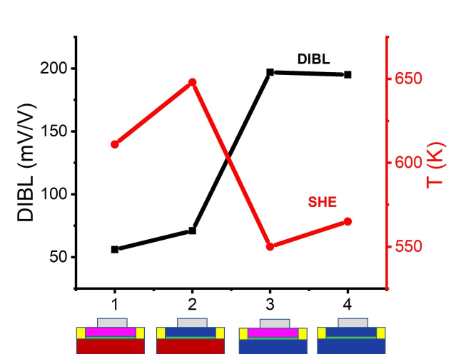
The dependence of the lattice temperature and DIBL on the combination number carried out from Figure 6 and Figure 7 for a gate length of 20 nm is shown in Fig 9. From the figure it can be seen that the SHE and the DIBL effect compete for the combination of the oxide materials. As we discussed above, the electrical and thermal properties of the back oxide material, namely the dielectric constant and the thermal conductivity, are mainly responsible for the SHE and DIBL effect in considered 2D-MoS2 MOSFETs.
Figure 9.
DIBL effect and SHE dependence of combinations of gate oxide and back oxide materials in MOSFET.
Figure 9.
DIBL effect and SHE dependence of combinations of gate oxide and back oxide materials in MOSFET.
Achieving the small DIBL effect requires a low dielectric constant back oxide material, while reducing the lattice temperature in the transistor channel requires a high thermal conductivity back oxide material. We have considered two popular, conventional used, back oxide materials: SiO2 and HfO2. When the back oxide material is SiO2, it has a small dielectric constant, which leads to a reduction in DIBL; at the same time, it also has a small thermal conductivity, which leads to a high lattice temperature in the transistor channel. Conversely, in the case of using HfO2 material as the back oxide material, it has a high dielectric constant, leading to a high DIBL effect, while it also has a relatively high thermal conductivity, leading to a reduction in the lattice temperature in the transistor channel.
From our results, it is possible to define the range of electrical and thermal parameters of oxide materials that allow reaching optimal immunity against SHE as well as the DIBL effect. From Figure 7, it can be concluded that using the BOX material with a relative dielectric constant in the range between 3.9 and 25, and with thermal conductivity between 1.4 and 2.3 W/Km is the choice for reaching optimal immunity. to degradation effects such as SHE and DIBL effects in 2D-MoS2-based MOSFET. Gate oxide material practically does not considerably impact to SHE as well as to DIBL effect.
4. Conclusions
Results of the simulation of the SHE effect show that at gate length less than 40 nm more impact to the resulting temperature has considered structures of the transistor (case 1 and case 2) than the impact of the gate oxide and BOX materials. SHE is sensitive to gate length for all combinations of the gate and back oxide materials in the transistor, while the DIBL effect is more sensitive to the gate length for transistors with combinations number 3 and 4.
The simulation results show that the choice of the gate oxide and BOX materials to ensure the possible highest immunity against degradation effects like SHE and DIBL effects is a task of optimization in 2D-MoS2-based MOSFETs. It is shown that the electrical and thermal properties of the back oxide material have the main influence on the SHE and DIBL effects in 2D-MoS2-based MOSFETs. Namely, using the BOX material with a relative dielectric constant in the range between 3.9 and 25, and with thermal conductivity between 1.4 and 2.3 W/(K∙m) allow reaching optimal immunity against degradation effects such as SHE and DIBL effects in 2D-MoS2 based MOSFET. Gate oxide material practically does not considerably impact to SHE as well as to DIBL effect..
Author Contributions
Conceptualization, A.E.A.; methodology, A.E.A., A.Y.; software, K.S.S.; validation, A.E.A. and K.S.S.; formal analysis, J.C.C. and A.Y; investigation, K.S.S.; resources, K.S.S; data curation, K.S.S.; writing—original draft preparation, A.E.A.; writing—review and editing, A.E.A. and J.C.C.; visualization, J.C.C., and A.Y.; supervision, A.E.A.; project administration A.E.A.; funding acquisition, A.E.A. All authors have read and agreed to the published version of the manuscript.
Funding
This research was funded by the Ministry of Innovation Development of the Republic of Uzbekistan, grant number Ind-Uzb-2021-80.
Conflicts of Interest
The authors declare no conflict of interest.
References
- B.Radisavljevic, A.Radenovic; J.Brivio, V.Giacometti, A.Kis, Single-Layer MoS2 Transistors, Nat.(2011) Nanotechnol 6, pp. 147– 150. [CrossRef]
- Z. Geng, Simulation of graphen nanoribbon and MoS2 transistors, Master Thesis (in German), TU Ilmenau (2016) pp. 3-17.
- H. Liu, A.T. Neal, P.D. Ye, Channel length scaling of MoS2 MOSFETs. ACS Nano(2012) 6(10), 8563–8569. [CrossRef]
- Tong, X., Ashalley, E., Lin, F. et al. Advances in MoS2-Based Field Effect Transistors (FETs). Nano-Micro Lett. 2015, 7, pp. 203–218. [CrossRef]
- Yao Guo, Xianlong Wei, Jiapei Shu, Bo Liu, Jianbo Yin, Changrong Guan, Yuxiang Han, Song Gao, and Qing Chen. Charge trapping at the MoS2-SiO2 interface and its effects on the characteristics of MoS2 metal-oxide-semiconductor field effect transistors Citation: Applied Physics Letters(2015) 106, 103109;. [CrossRef]
- A.E. Atamuratov, B.O. Jabbarova, M.M. Khalilloev, K. Sivasankaran, J.C. Chedjou, Impact of the channel shape, back oxide and gate oxide layers on self-heating in nanoscale JL FINFET Nanosystems: Physics, Chemistry, Mathematics, 2022, 13(2), pp. 148–155.
- A.E. Atamuratov, B.O. Jabbarova, M.M. Khalilloev, A. Yusupov,. The Self-Heating Effect in Junctionless Fin Field-Effect Transistors Based on Silicon-on-Insulator Structures with Different Channel Shapes Technical Physics Letters, 2021, 47(7), pp. 542–545. [CrossRef]
- A.E. Atamuratov, B.O. Jabbarova, M.M. Khalilloev, A. Yusupov, A.G. Loureriro, Self-heating effect in nanoscale SOI Junctionless FinFET with different geometries Proceedings of the 2021 13th Spanish Conference on Electron Devices, CDE 2021, 2021, pp. 62–65, 9455728.
- A. E. Atamuratov, X. S. Saparov, T. A. Atamuratov, A. Yusupov and F. Schwierz, "The contribution of gate and drain voltages to temperature distribution along the channel in 2D MoS2 based MOSFET," 2021 International Conference on Information Science and Communications Technologies (ICISCT), 2021, pp. 01-03. [CrossRef]
- S. Tiwaria, S. Dolaia, H. Rahamana, P.S. Guptaa, Effect of Temperature & phonon scattering on the Drain current of a MOSFET using SL-MoS2 as its channel material, Superlattices and Microstructures (2017). [CrossRef]
- R. Granzner, Z. Geng, W. Kinberger and F. Schwierz, "MOSFET scaling: Impact of two-dimensional channel materials," 2016 13th IEEE International Conference on Solid-State and Integrated Circuit Technology (ICSICT), (2016), pp. 466-469. [CrossRef]
- N. D. Bharathi and K. Sivasankaran, 2018 Influence of metal contact on the performance enhancement of monolayer MoS2 transistor Superlattices Microstruct. 120, pp. 479–86.
- Matthew A.Panzer, Michael Shandalov, Jeremy A. Rowlette, Yasuhiro Oshima, Yi Wei Chen, Paul C. McIntyre, and Kenneth E. Goodson. Thermal Properties of Ultrathin Hafnium Oxide Gate Dielectric Films. IEEE Electron Device Letters, vol. 30, no. 12, december 2009, pp. 1269-1271. [CrossRef]
- C. Stolz, F. Genin, T. Reitter, N. Molau, R. Bevis, M. Gunten, D. Smith, and J. Anzellotti, Effect of Si02 overcoat thickness on laser damage morphology of HfO2 ISiO2 Brewster’s angle polarizers at 1064 nm. (1997) Proc. SPIE 2966, p. 265. [CrossRef]
- R.Kato, & I.Hatta, Termal Conductivity Measurement of Termally-Oxidized SiO2 Films on a Silicon Wafer Using a TermoRefectance Technique. (2005) International Journal of Termophysics 26, pp. 179–190. [CrossRef]
- Birgit Ryningen, Martin P. Bellmann, Rannveig Kvande, Otto Lohne. The effect of crucible coating and the temperature field on minority carrier lifetime in directionally solidified multicrystalline silicon ingots. 27th Eeuropean Photovoltaic Solar Energy Conference and Exhibition. Conference paper January 2012, pp. 926-932. [CrossRef]
Figure 1.
Ig-Vd characteristics of the considered 2D-MoS2 based MOSFETs with different gate lengths. The gate oxide material is Al2O3, and the BOX material is SiO2 with thickness 1020 nm. The Drain voltage is Vd = 1V. Solid lines correspond to results in [2], and colored marks are the results of our simulation.
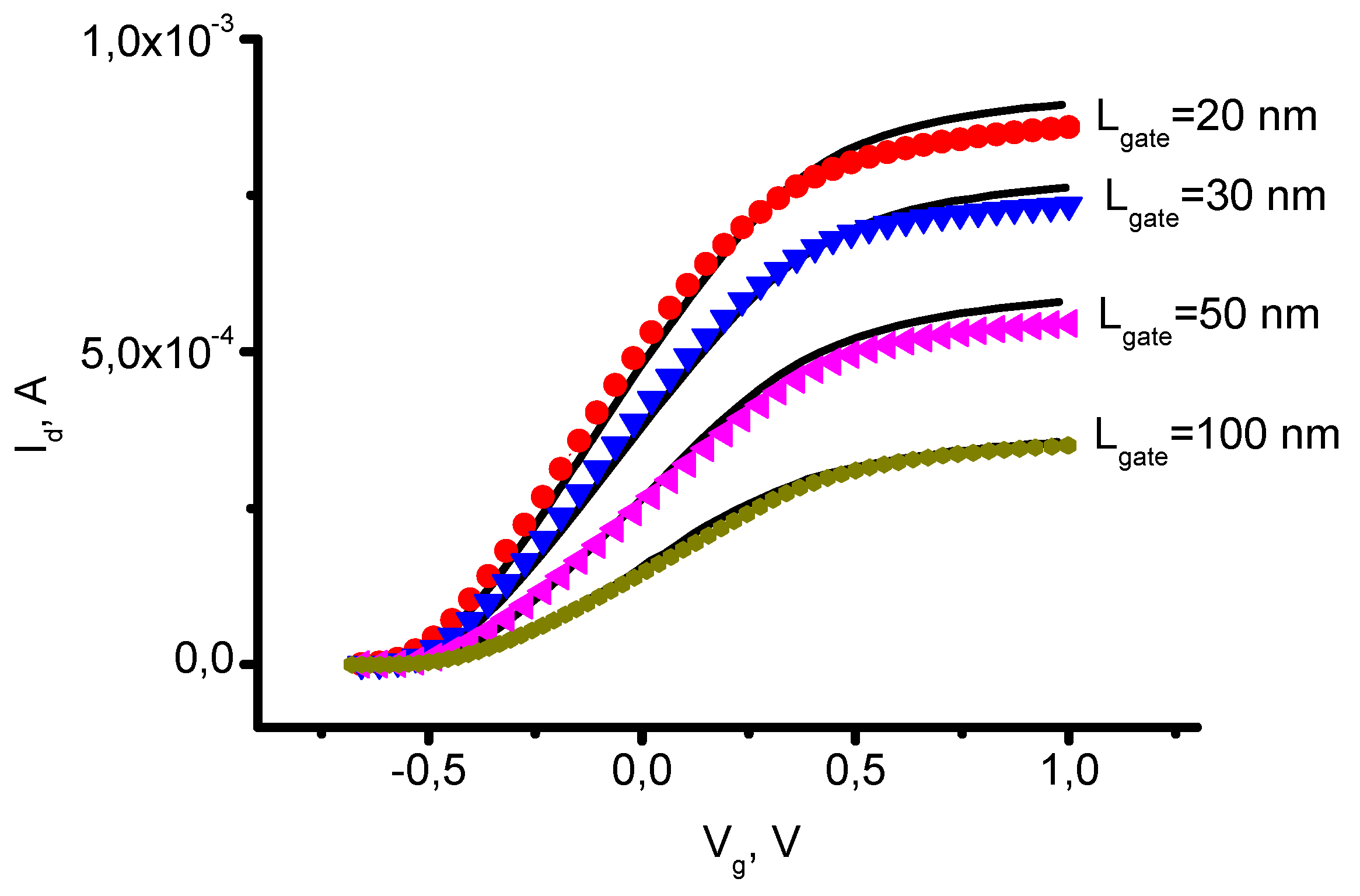
Figure 2.
Structure of the simulated MoS2 MOSFET. Two cases are considered: (a) the gate oxide length is equal to the MoS2 channel length (first case); (b) the gate oxide length is equal to the gate length (second case).
Figure 2.
Structure of the simulated MoS2 MOSFET. Two cases are considered: (a) the gate oxide length is equal to the MoS2 channel length (first case); (b) the gate oxide length is equal to the gate length (second case).
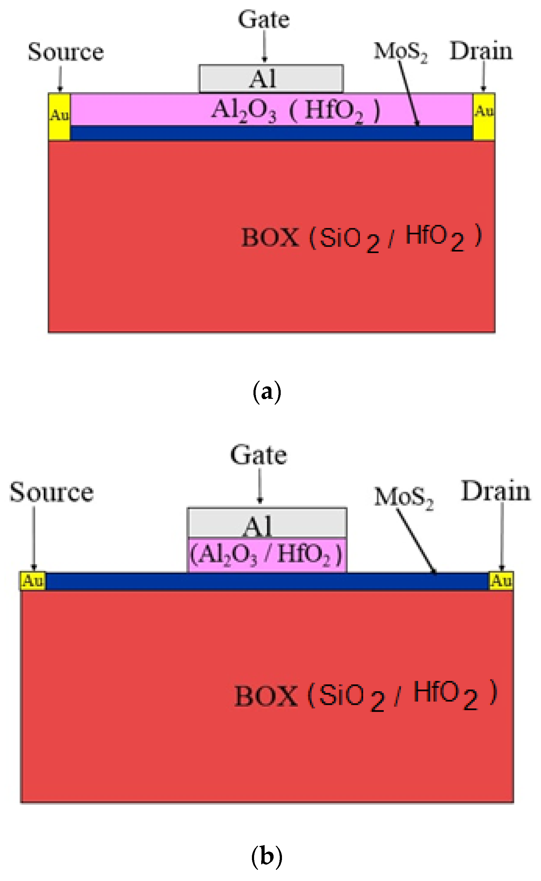
Figure 3.
Dependence of the lattice temperature in the center of the channel on the gate length for 2D MoS2 MOSFETs with Al2O3 gate oxide (1.2) and HfO2 gate oxide (3.4) with fully covered channel top (2.4) and with partially covered channel top (only under the gate) (1,3).
Figure 3.
Dependence of the lattice temperature in the center of the channel on the gate length for 2D MoS2 MOSFETs with Al2O3 gate oxide (1.2) and HfO2 gate oxide (3.4) with fully covered channel top (2.4) and with partially covered channel top (only under the gate) (1,3).
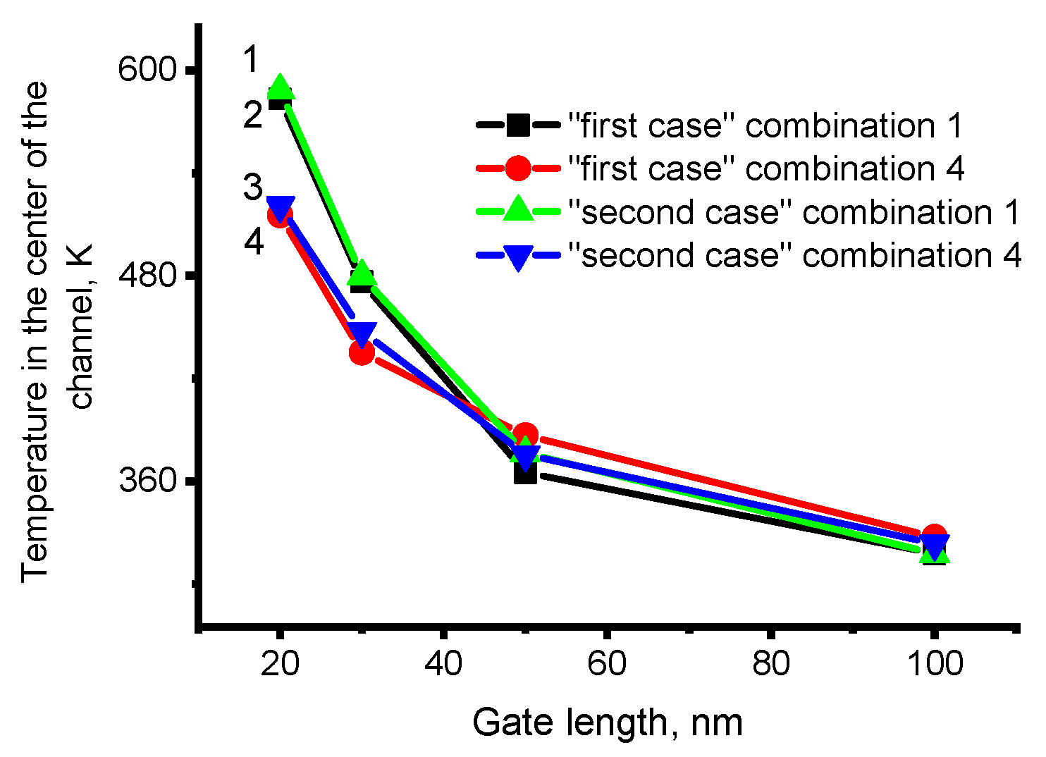
Figure 4.
Distribution of temperature along the channel for the “first case” transistors with gate oxide materials Al2O3 and HfO2, while BOX material is SiO2 and HfO2 respectively. The gate lengths is 20 nm (a) and 100 nm (b). Vg=0.1 V and Vd=0.4 V.
Figure 4.
Distribution of temperature along the channel for the “first case” transistors with gate oxide materials Al2O3 and HfO2, while BOX material is SiO2 and HfO2 respectively. The gate lengths is 20 nm (a) and 100 nm (b). Vg=0.1 V and Vd=0.4 V.
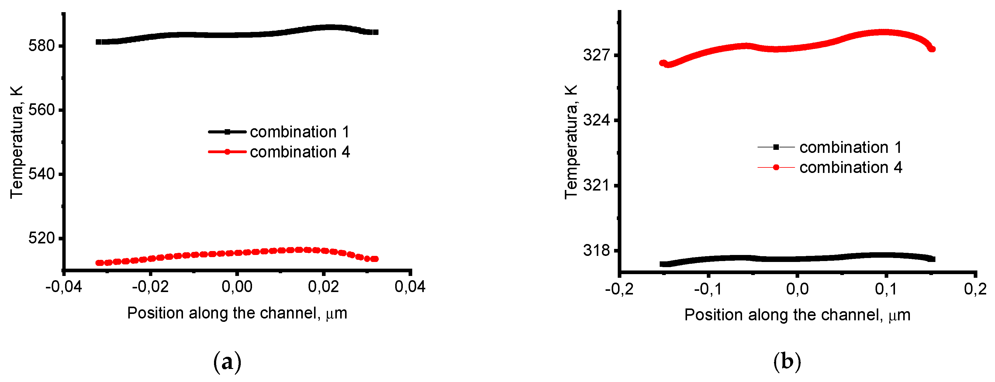
Figure 5.
Distribution of temperature along the channel for the “second case” transistors with gate oxide materials Al2O3 and HfO2, while BOX material is SiO2 and HfO2 respectively. The gate lengths are 20 nm (a) and 100 nm (b). Vg=0.1 V and Vd=0.4 V.
Figure 5.
Distribution of temperature along the channel for the “second case” transistors with gate oxide materials Al2O3 and HfO2, while BOX material is SiO2 and HfO2 respectively. The gate lengths are 20 nm (a) and 100 nm (b). Vg=0.1 V and Vd=0.4 V.
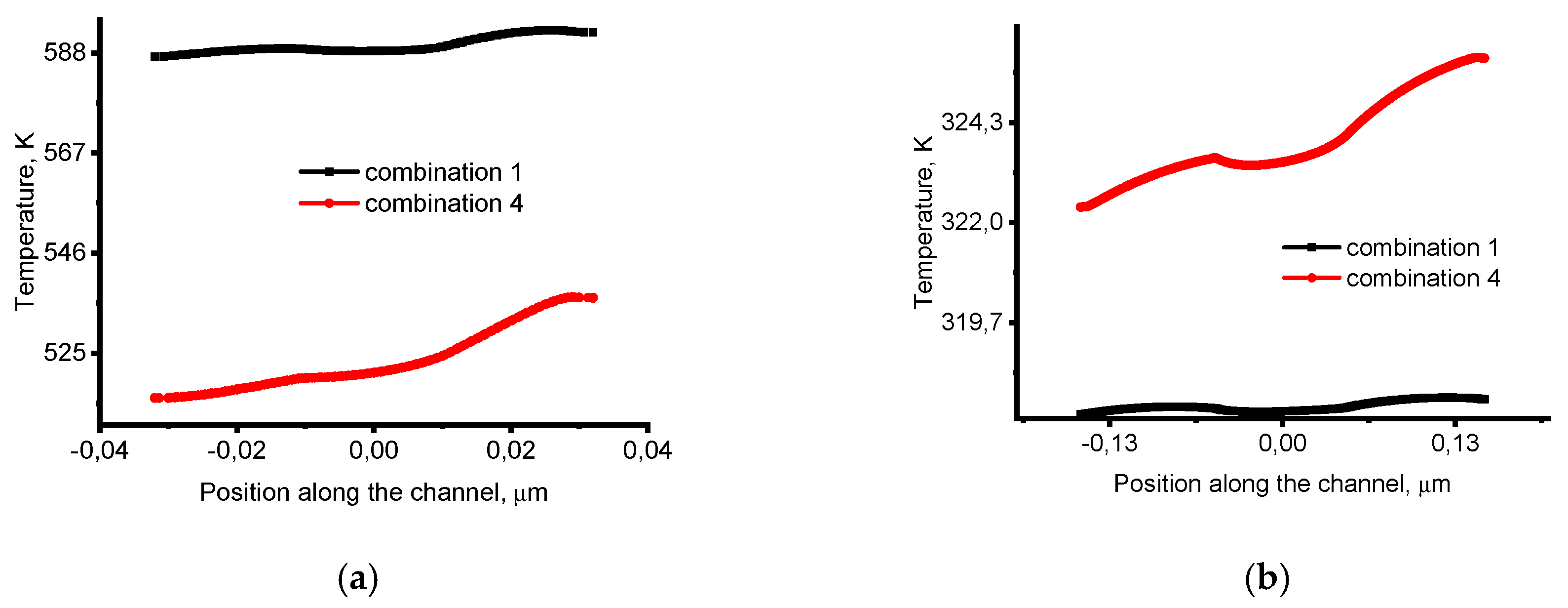
Figure 6.
SHE dependence on the gate length for different combinations of gate oxide and back oxide materials.
Figure 6.
SHE dependence on the gate length for different combinations of gate oxide and back oxide materials.
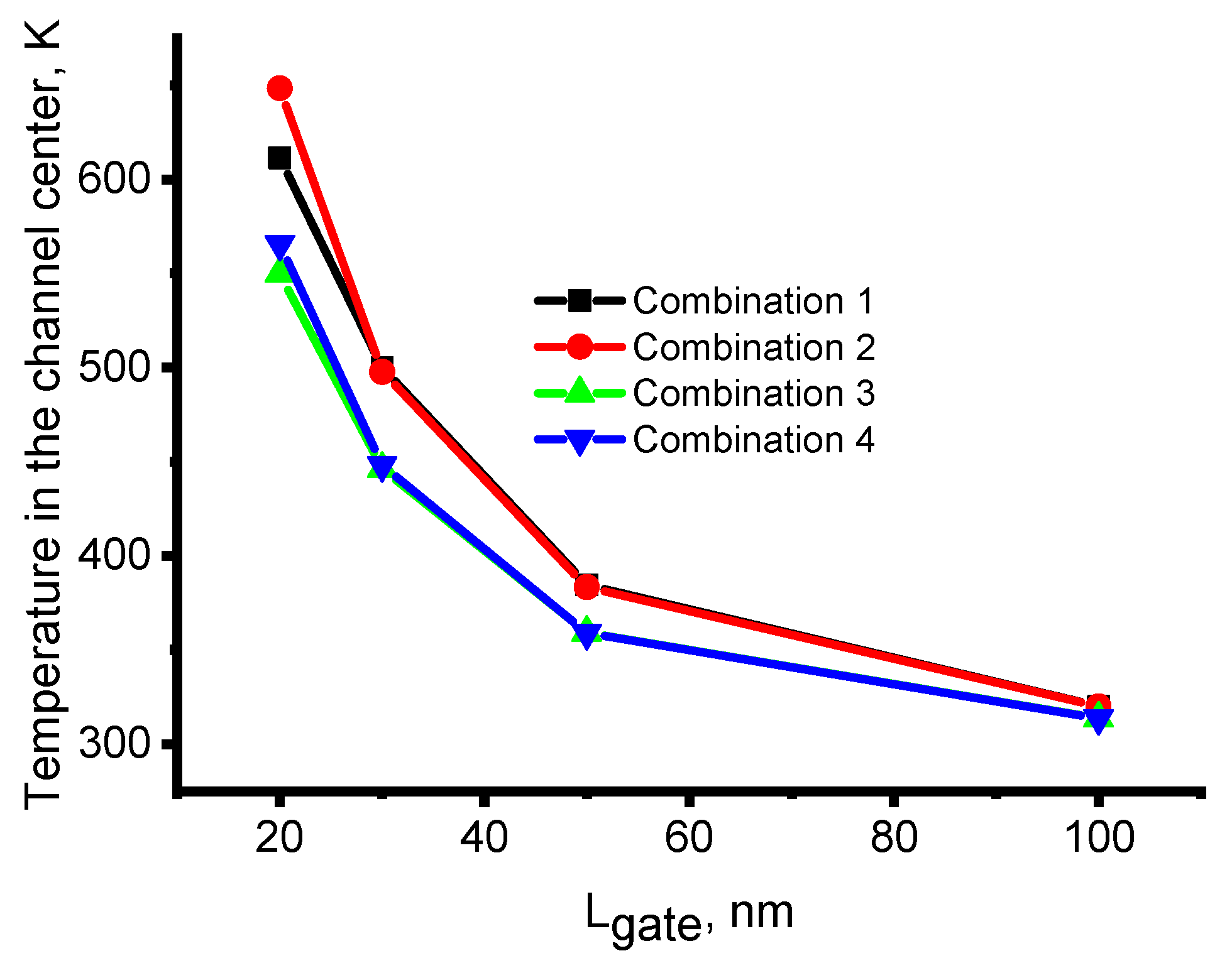
Figure 7.
DIBL effect dependence on the gate length for different combinations of gate oxide and back oxide materials.
Figure 7.
DIBL effect dependence on the gate length for different combinations of gate oxide and back oxide materials.
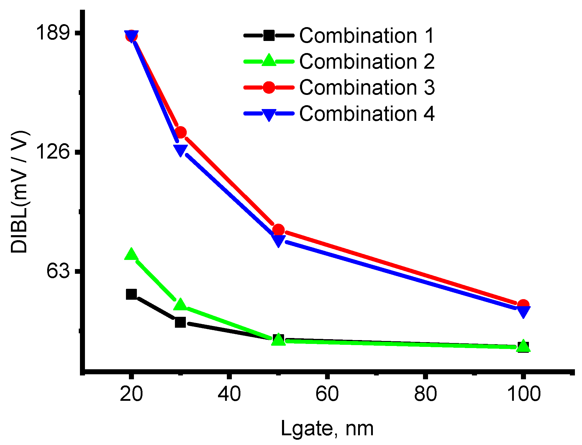
Figure 8.
Equivalent circuit describing the capacitive coupling between the channel and the device electrodes in MOSFET.
Figure 8.
Equivalent circuit describing the capacitive coupling between the channel and the device electrodes in MOSFET.
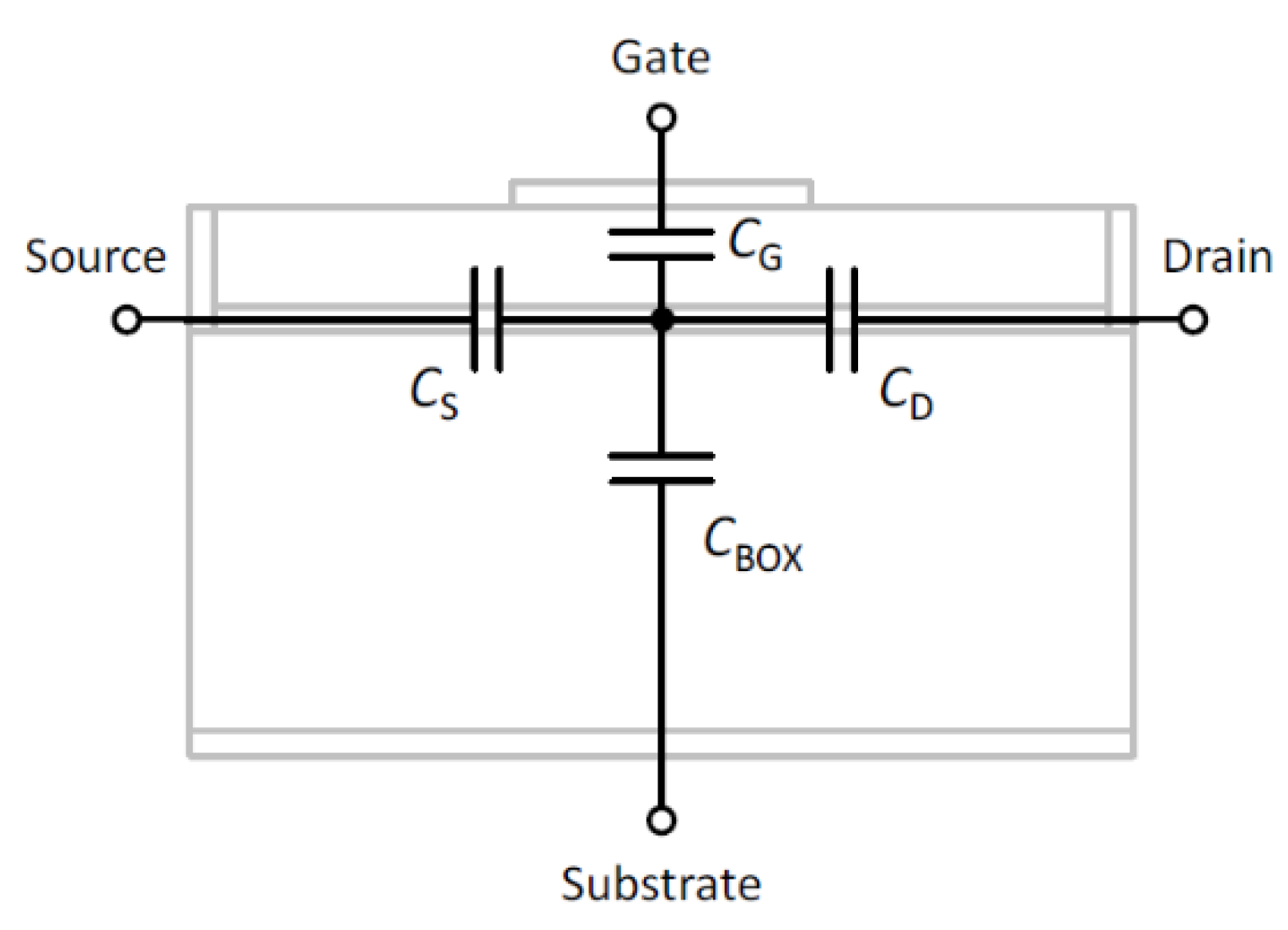

Table 1.
Combination of the gate and back oxide materials considered in the work.
| Number of combination | Gate oxide material | Back oxide material |
| 1 | Al2O3 | SiO2 |
| 2 | HfO2 | SiO2 |
| 3 | Al2O3 | HfO2 |
| 4 | HfO2 | HfO2 |
Table 2.
Thermal conductivities used for simulation.
| Material | Thickness (nm) |
Thermal conductivity |
| SiO2 | 80 | 1.4 |
| Al2O3 | 2.385 | 12 |
| HfO2 (gate oxide) | 5.641 | 2.3 |
| HfO2 (Box) | 80 | 2.3 |
Disclaimer/Publisher’s Note: The statements, opinions and data contained in all publications are solely those of the individual author(s) and contributor(s) and not of MDPI and/or the editor(s). MDPI and/or the editor(s) disclaim responsibility for any injury to people or property resulting from any ideas, methods, instructions or products referred to in the content. |
© 2023 by the authors. Licensee MDPI, Basel, Switzerland. This article is an open access article distributed under the terms and conditions of the Creative Commons Attribution (CC BY) license (http://creativecommons.org/licenses/by/4.0/).
Copyright: This open access article is published under a Creative Commons CC BY 4.0 license, which permit the free download, distribution, and reuse, provided that the author and preprint are cited in any reuse.


