1. Introduction
Photonic technology has undergone a boost in the last couple of decades. Photonics has come forward to replace electronic technology in various applications due to its power efficiency and ability to operate in Terahertz (THz) frequency ranges. Specifically, mentioning the optical integrated components such as switches [
1], modulators [
2], multiplexers [
3], logic gates [
4,
5], and filters [
6] which play an essential role in an optical integrated circuit, have become the center of research nowadays. Researchers are busy digging down the architecture and topology for the photonic integrated circuits (PICs) keeping in view the process-related complexity, performance, and fabrication as a whole. Considering optical technology as the best alternative to electronic technology [
7], the optical fields are brought together to use different phenomena such as the interference [
8], Guided mode resonances (GMR) [
9], Kerr effect [
10], and many more [
11]. Moreover, the proper choice of materials is a key factor in designing an optical device. Among periodic nanostructures, Photonic Crystals (PhCs), have recently flattened the way nearer to the achievement of optical integrated circuits. PhCs are the periodic dielectric nanostructures that are capable of controlling the light at wavelength scale [
12]. The concept of the PhCs is derived from nature, presenting themselves on the bodies of different living organisms i.e., insects, parrots, peacocks, and stones [
13]. They exhibit different phenomena of light in terms of reflection, refraction, diffraction, and total internal reflection [
14]. PhCs can be created artificially to design, produce and achieve what is required of a certain component or a device in the existing world [
15].
Considering the components of the PIC, an optical switch is an important element that can work analogous to the electronic transistor in the electronic integrated circuits. Therefore, utmost efforts are made to achieve the functions of optical switching element using the time domain [
16] or frequency domain [
17], with different topologies in the form of cross waveguide geometries [
18], quantum dots [
19], optoelectronic hybrid devices [
20], ring resonators [
21], combined configurations of thermodynamics and optical components [
22] and utilization of transparent and active materials [
23,
24], with it desired working and implementation in the optical circuits. A 2D-FDTD design of an optical switch is investigated in [
25], by means of the phenomenon of GMR with varying radius cavity implemented at the start of the PhC-mesh. Another approach uses GMR modes to achieve optical switching using the changeable radius cavity within the middle of the PhC-mesh [
26,
27]. An optical switch using two linear waveguides and a circular geometry of the PhCs is studied in [
28], using temperature as the variable quantity for the switching mechanism in terms of a shift in the resonance wavelength. Using the broken mirror symmetry to obtain asymmetric Fano-shapes is given in [
29], utilizing partially transmitting material within the waveguide to propose an optical switching device and its prospects [
30]. A four-port optical switch is investigated in [
31], using the square lattice of the PhCs and rods of gallium phosphide with a medium composed of air, metallic embedding nanowires [
32], using Finite Difference Time Domain (FDTD) approach and a thermo-optic effect with super-ellipse shape [
33]. A similar idea is perceived in [
34], using the Plane-wave expansion (PWE) approach to estimate the bandgap of the optical switching device with a discussion of its applications in optical decoders [
35]. Based on the design of the 2D PhC-cavity structure and its transmission spectra, an optical switching device is investigated by uttering the Kerr effects to produce a shift in its resonant wavelength given in [
36], using III-V nanowires on Silicon (Si) platform for the purpose [
37], strong carrier-induced nonlinearity [
38], defect rods made of doped glass [
39], free-carrier induced dispersion [
40] and a non-linear cavity coupled to input and output of the waveguide [
41].
Similarly, using Quantum Dots (QDs) to observe the mechanisms of optical switching and achieve higher rates of transmittance and flat bandwidth using latch function is premediated in [
42] and through Symmetric Mach Zehnder (SMZ) type in [
43]. Plasmonics effects are utilized for optical switching using a strip of graphene layer onto a structure of PhCs in [
44] and the mechanism is investigated using graphene rods in [
45]. An approach of using concepts of mott phase change material in PhCs-based structure responsible for the shifting of the optical bandgap is investigated in [
46] and using polymer waveguides with high thermos-optic and electro-optic in [
47]. Similarly, a 3D Si-opal composite is reported in [
48], with a pump-probe technique in [
49], and 1D graphene-based plasmonics crystals in [
50], to efficiently pronounce the effects of optical switching. Apart from these, using two PhC-cavities within one arrangement is reported in [
51], using a waveguide between them. Thus, coupling a probe signal in the waveguide, affects the field distribution and quality factor of both of the PhC-cavities, enabling the structure to be comprehended as an optical switch. Soft PhCs in the form of chiral liquid crystals are also used for obtaining certain properties of the optical switch, as described in [
52], while through effects of physics in terms of parity-time symmetry and topological insulators in [
53], using phase change nanomaterials [
54], air-trench [
55] and carrier diffusion and recombination processes in PhCs [
56], with the design based on 3D Micro-Electro-Mechanical-Systems (MEMS) reported in [
57].
This research investigates the design of the 3D-optical switch working in the near-infrared region (NIR), suitable for communication systems. Moreover, is implemented using the 3D-FDTD domain and the interference phenomenon between the GMR modes and index guided-modes inside a slab-waveguide PhC structure. For this purpose, the proposed device uses two optical signals i.e., data and control. The data signal is integrated into the optical structure by means of the out-of-plane method i.e., GMR, and is amplified or de-amplified using a control signal, that is index guided into the slab-waveguide structure.
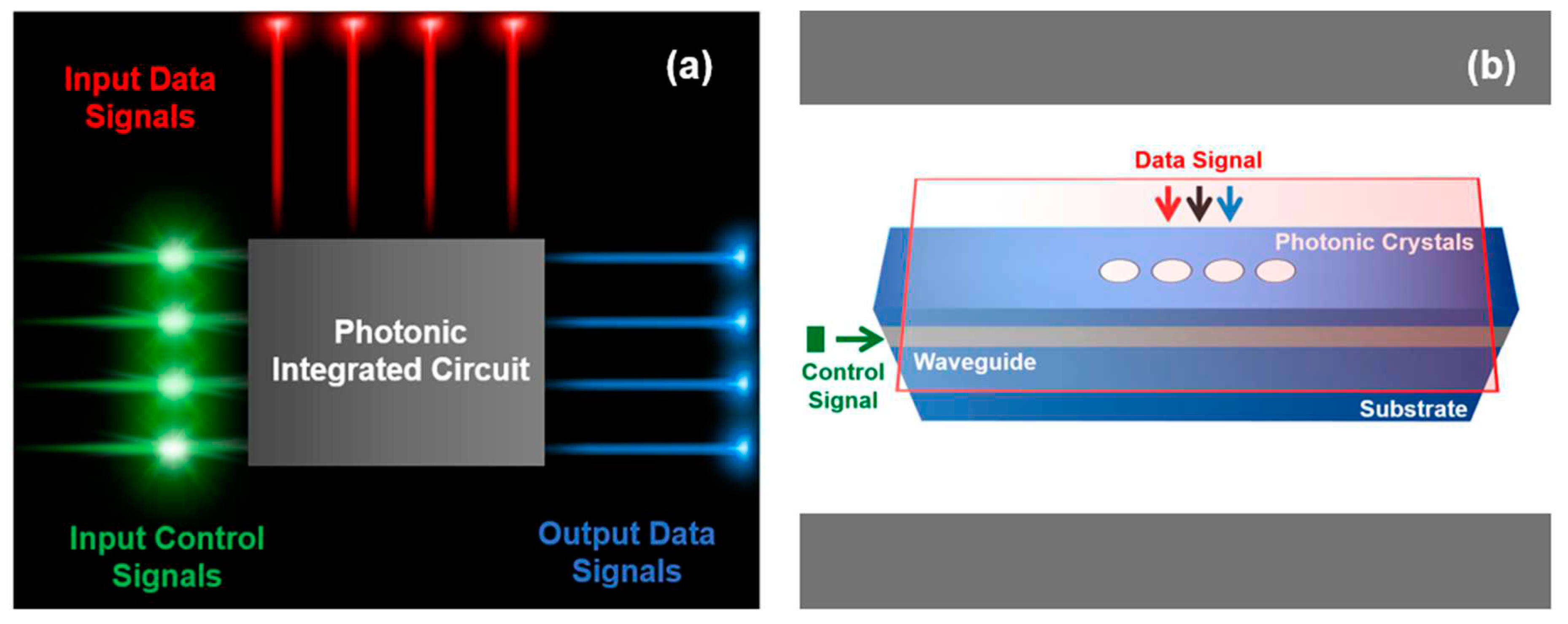
Figure 1(a) imitates the theoretic 3D structure of the optical switch, presenting an innovative, compact, easy-to-fabricate, and implementable device. Likewise, due to lower absorption by the dielectric-materials, is suitable for broad spectral ranges, contrasting semiconductors having higher material-cost and absorption, making their use and fabrication difficult in densely populated optical integrated circuits as investigated in previous studies.
Figure 1(b) illustrates the use of the proposed optical switch in an optical integrated circuit. Therefore, finds applications in the field of optical integrated components, filters, sensors, quantum computing, and communication systems.
2. Simulation Approach
The 3D-FDTD simulation of the proposed structure is performed using the MIT Electromagnetic Equation Propagation (MEEP) software [
58], an open-source platform, based on the FDTD domain [
59]. Therefore, during execution the desired arrangement is transformed initially into a finite-arrangement of grids known as the YEE grids [
60], to compute the Electric ‘E’ field and Magnetic ‘B’ field based on Maxwell’s equations. Moreover, FDTD is advantageous in terms of computing the response of the system in a single run (using a short Gaussian pulse), providing the user with the propagation of the wave both in near-field and far-field especially inside complex structures like PhCs [
61]. Apart from these, requires fewer-computational resources, memory, and time as related to frequency domain-based simulations [
62].
3. Design Parameters
The optimized design parameters of the proposed 3D-optical switch are given in
Table 1 in terms of lattice-constant ‘a’ chosen as (a = 1 µm), serving two purposes i.e., to enable the designing of the device scalable to any range of wavelength and enable its operation in the telecommunication window around 1. 55 µm, using cylindrical shaped-based PhCs-elements.
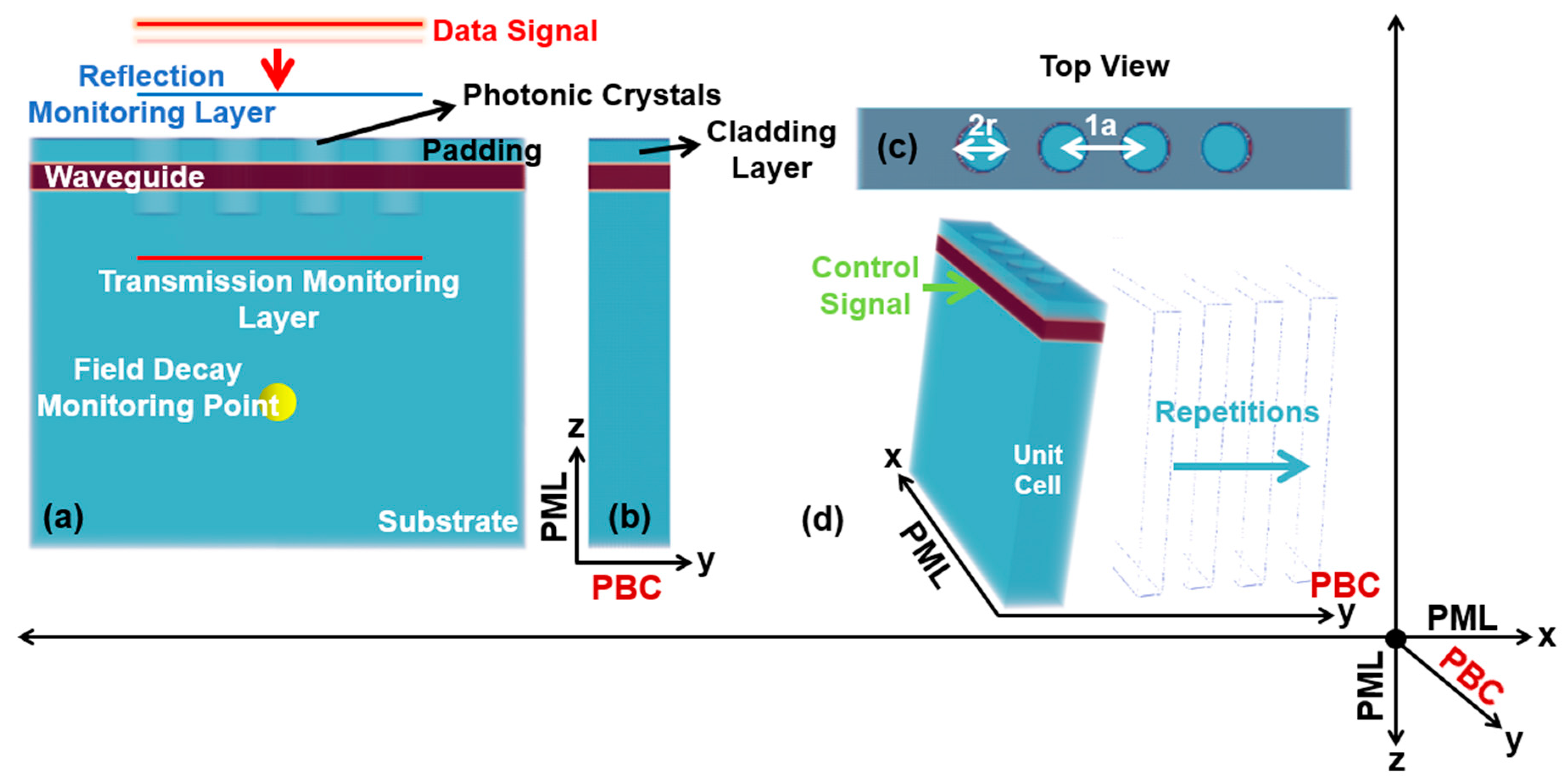
Figure 2, imitates the design of the proposed 3D-optical switch using Niobium pentaoxide (Nb
2O
5) as the waveguiding material, with a refractive index of n
wav = 2.2 [
25], and is deposited on a substrate made-up of Silicon dioxide (SiO
2) with a refractive index as n
sub = 1.5 [
27], along a cladding layer of the SiO
2 placed topmost of the waveguiding layer. Moreover, is the representation of a strip model of the 3D-optical switch, based on which, the investigations are performed and two final models are computed in the end.
For the data signal, a Gaussian time profile source is used, located at a range of 2.7a above the waveguide, with a similar profile-source for control signal index guided in the optical structure from the lateral-side using a user definite sum of frequencies ‘nf’ as (nf = 550) for both of the sources. Similarly, the transmission and reflection monitoring layers are positioned at a range of 1.0a below and above the waveguide respectively, to compute the electromagnetic (EM) fields. For the purpose to terminate the simulation process, a field decay monitoring point is positioned at a user-definite distance of 1.5a. To observe the behavior and prevent back-and-forth of the EM fields at the boundaries of the structure, the Perfectly Matched Layers (PML) are implemented along x-z axes. Moreover, to save time and computational-resources, the Periodic Boundary Condition (PBC) is used on the y-axis. However, this condition of the PBC is removed and is replaced by PML, during the simulation of the finite structures of the 3D-optical switch.
4. Results
The 3D-FDTD simulation of the optical switch is performed in this research work, using the stripe model criterion. For this purpose, the first step is determining the number of the PhC-elements using a single source i.e., the data signal only, to tune the GMR modes around the resonant wavelength i.e., 1.55µm.
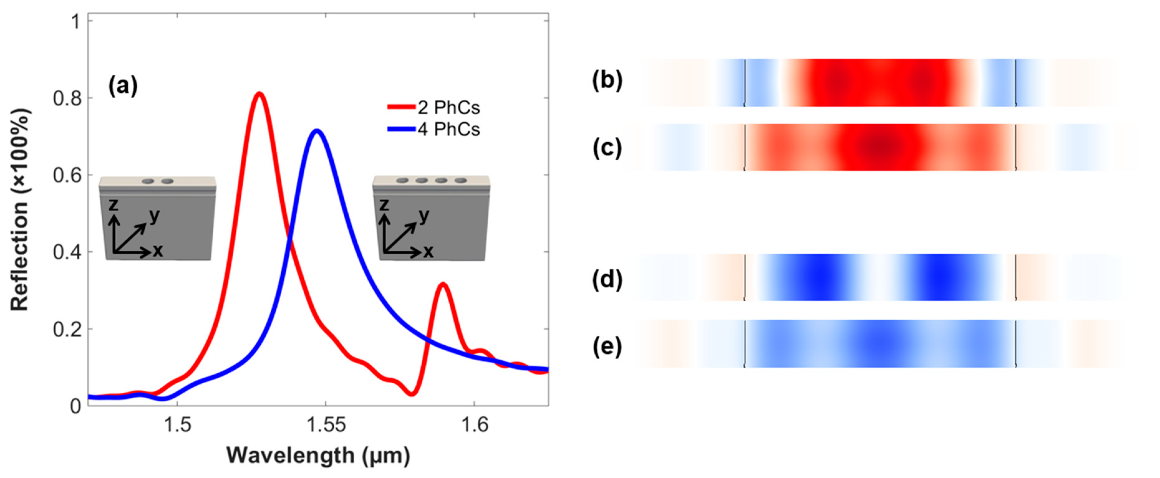
Figure 3(a), imitates output reflection spectra of the structure comprising of 2 and 4 PhC-elements, respectively. Therefore, it can be seen that the structure based on 2 PhC-elements has a higher intensity of reflection peaks, as compared to 4 PhC-elements-based structure. However, it is worth noting here from the output spectra, that the resonant wavelength of the 2 PhC-elements-based arrangement is around 1.528µm, while is at 1.547µm in the 4 PhC-elements-based structure. Similarly,
Figure 3(b-c) and
Figure 3(d-e) show the Electric ‘E’ and Magnetic ‘B’ fields confinement by the structures comprising of 2 and 4 PhC-elements respectively, with
Table 2, presenting the detailed comparisons between them.
Apart from the change in reflection peaks and resonant wavelength, there is a visible difference in the linewidth and the quality factor between these two structures. Correspondingly, to linewidth, it remains low in the 2 PhC-elements-based arrangement and a bit on the higher side in the 4 PhC-elements-based structure. Similarly, the quality factor is higher in the former structure and vice versa. However, each arrangement possesses their pros and cons, which can be entangled during the designing of the 3D optical switch. As an acknowledgeable fact, the number of the PhC-elements can be increased, as it may pronounce more confined GMR modes using data signal only but is limited to 4 PhC-elements only, due to the fact, that it will in turn reduce the outcomes of the control signal on the output of the data signal. In other words, it will reduce the switching properties of the device equivalent to the depletion-region of the electronic-transistor. Apart from these, further structuring in the 3D domain relating to an increase in the number of PhC-elements is also limited by the computational resources in terms of speed and memory. As a result, achieving the unity factor in the output spectra is hindered. Similarly, the propagation losses incurred by the control signal due to gratings also contribute to the fact and are added to absorption-losses of the materials. Henceforth, both of the arrangements are investigated for the operations of optical switching and concluded with two 3D finite structures of the device based on 2 and 4 PhC-elements in the end.
3.1. Study of Optical Switching Phenomenon by differing the number of PhC-elements using Data and Control Signals Simultaneously
To investigate the phenomena of the optical switching in 3D PhC-elements-based structures i.e., 2 and 4 PhC-elements, the control signal is executed along with the data signal for the purpose. Besides, the wavelength of the control signal is also varied to investigate its detailed response on the output of the data signal.
Table 3, shows the criterion used in changing the wavelength of the control signal w.r.t data signal.
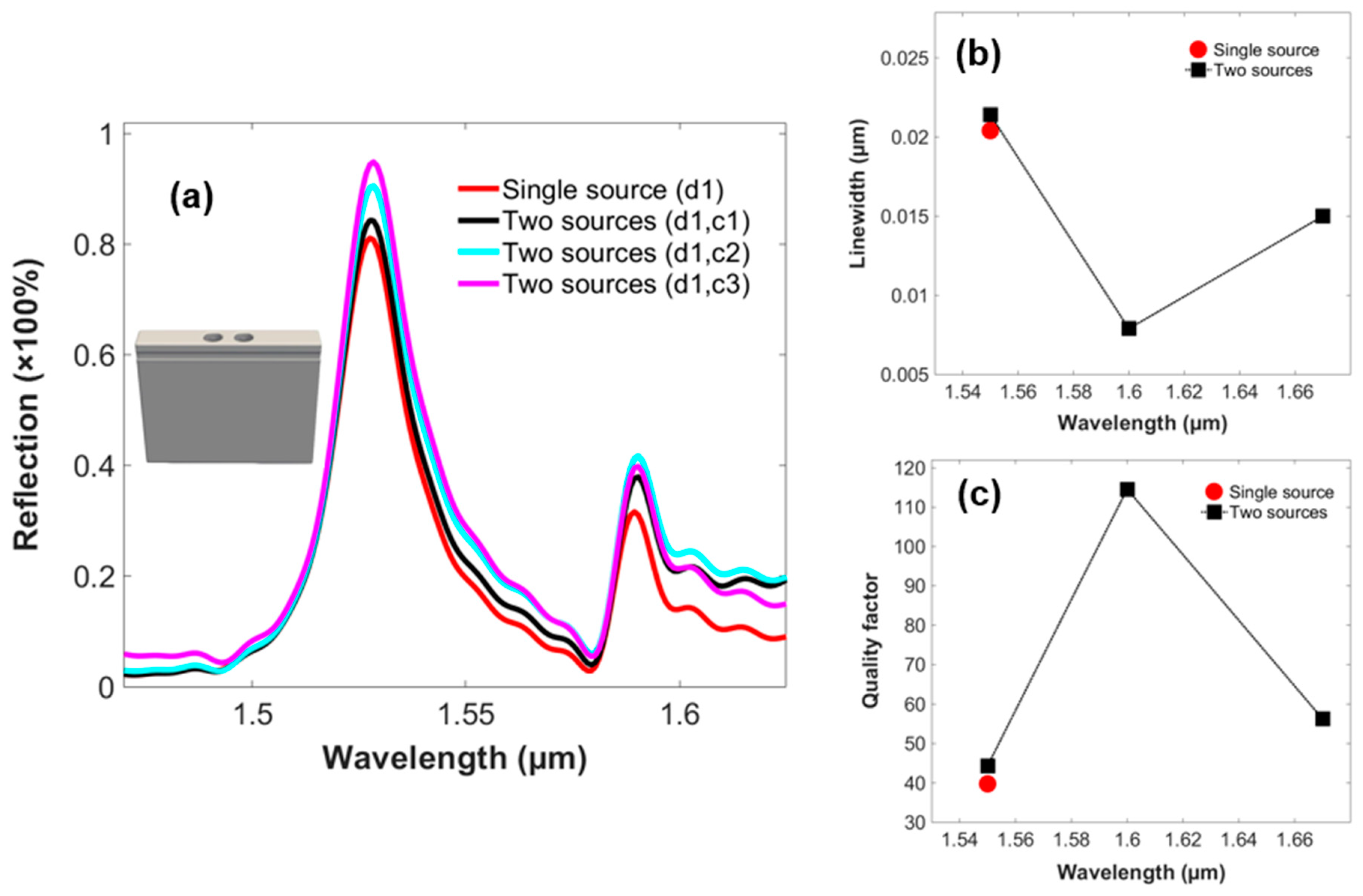
The effects of the control signal are given in the reflection spectra of 2 PhC-elements-based structure in
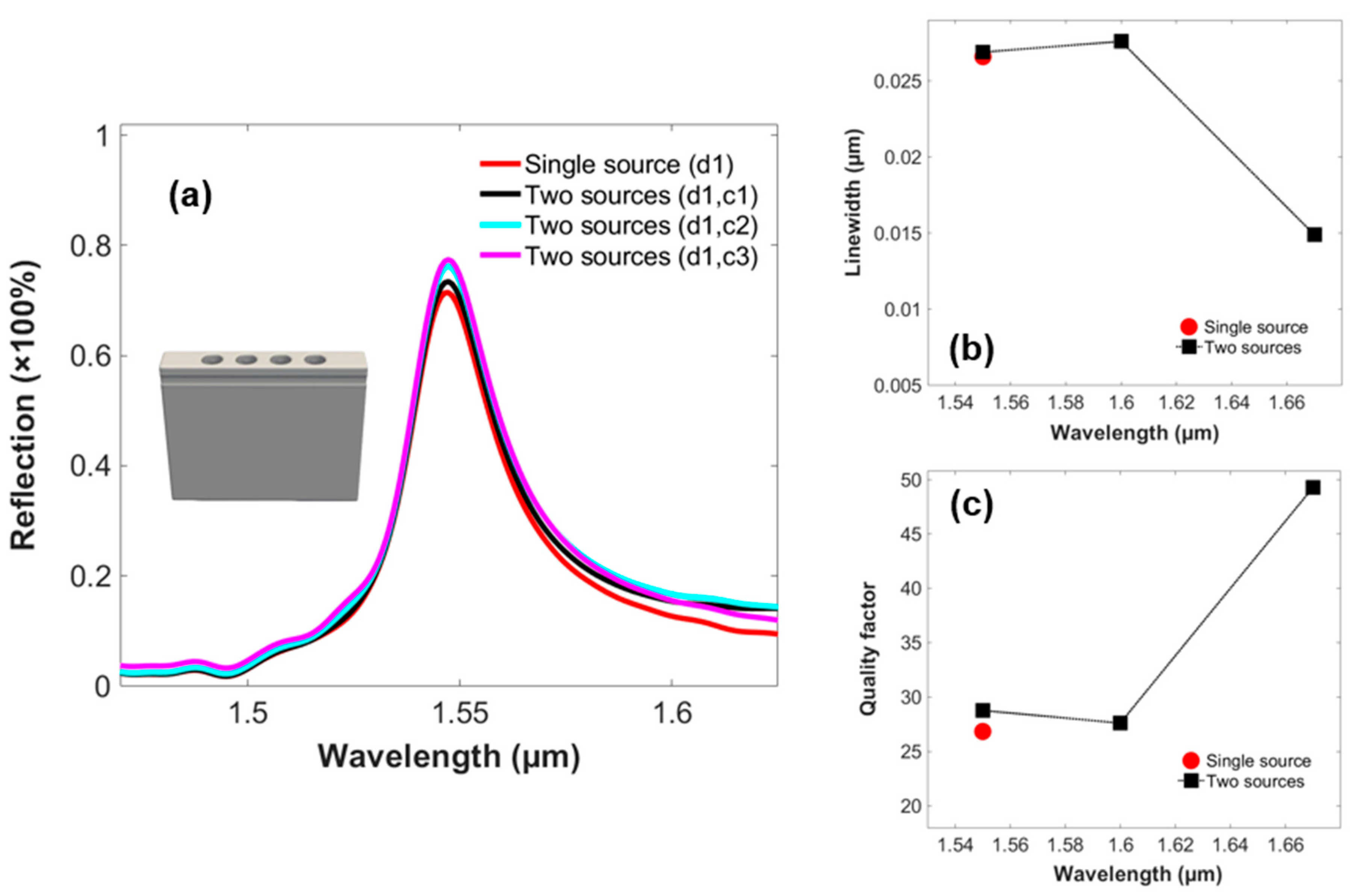
Figure 4(a). It investigates the increase in the percentage of the reflection peaks as the wavelength of the control source is varied from 1.67 µm to 1.55 µm and vice versa. It presents a prominent change for the control source at a wavelength of 1.55 µm.
Figure 4(b), illustrates the alteration in the linewidth of the structure as the wavelength of the control signal is varied, reporting the lowest value of 0.0079µm, at a wavelength of 1.60 µm of the control signal.
Figure 4(c), presents the quality factor of the structure achieving a maximum value of 112, concerning the control source at a wavelength of 1.60µm. Thus, the GMR modes are confined and offer higher selectivity for the 2 PhC-elements structure, with the control signal at a central wavelength of 1.60µm implemented along the data signal.
Similarly,
Figure 5(a), investigates the 4 PhC-elements-based structure for optical switching action. Therefore, it can be seen, that implementing the control signal along the data signal increases the coupling of the GMR modes and energy further into the optical structure and as a result, reaches nearer to the desired resonant wavelength of the structure i.e., 1.55 µm. Moreover, it achieves higher percentages of reflection spectra, when the wavelength of the control signal is varied from 1.67 µm-1.55 µm and is maximum, when this wavelength is equivalent to the wavelength of the data signal i.e., 1.55 µm.
Figure 5(b), imitates the variation in the linewidth of the structure based on 4 PhC-elements, achieving a minimum value of around 0.0149µm, at a wavelength of 1.67 µm of the control signal.
Figure 5(c), reports the variation in the quality factor w.r.t change in the wavelength of the control signal. Therefore, it can be investigated, that the structure achieves the maximum value of quality factor i.e., 49.28 at 1.67 µm wavelength of the control signal. Therefore, the optimum figure of the wavelength of the control signal is 1.60 µm and 1.67 µm for the 2 and 4 PhC-elements-based structures respectively.
Table 4, shows the detailed responses of both of the topologies in terms of resonant wavelength, reflection, linewidth, and quality factor.
3.2. Finite Structures of the 3D Optical Switch Based on 2 and 4 PhC-elements
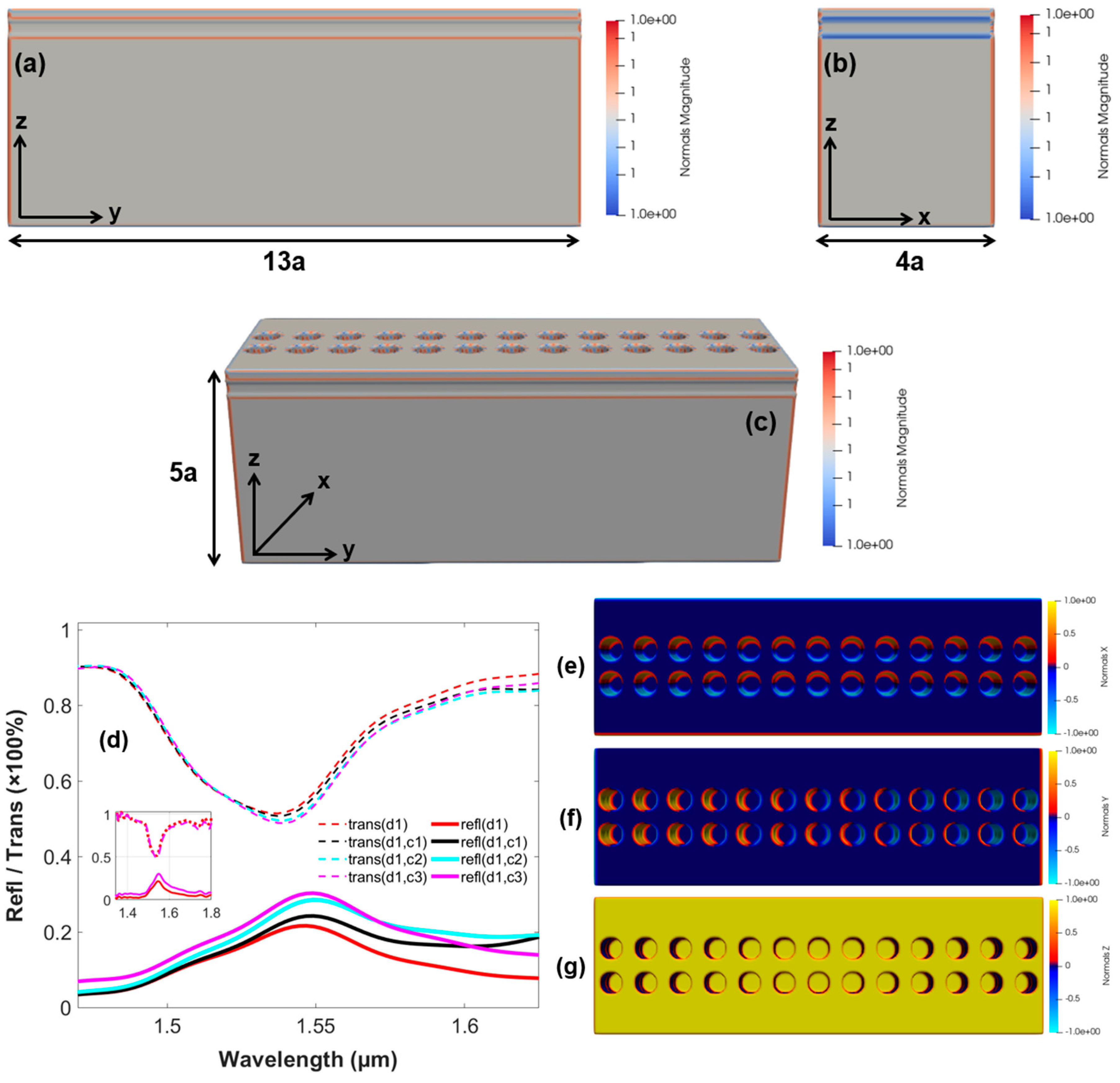
The next step is to investigate and draw finite structures of the 3D optical switch, by removing the PBC, previously implemented on the y-axis, in the case of the striped model. Moreover, instead, the PML is executed on all of the three axes, for finite realization of the device. For this purpose, the 2 PhC-elements-based structure is realized first as shown in 6(a-c), depicting the length, width, and height of the device.
Therefore, for the optical switching mechanism, the structure is simulated using data and control signals simultaneously, with reflection and transmission spectra imitated in
Figure 6(d). So, it can be shown from the spectra, that by implementing the control signal and varying its wavelength from 1.67µm-1.55µm, the output of the data signal tends to increase and vice versa. Thus, helping in the confinement of GMR modes and energy. However, it is worth noting here, that the intensity and coupling of energy of the resonant modes is lower to a certain degree as in comparison to the striped model of the 2 PhC-elements-based structure. Henceforth, it can be increased and the desired level can be achieved by increasing the number of PhC-elements along (y-axis), which is limited by the computational resources at present.
Figure 6(e-f), shows the field confinement of the structure along (x and y) directions, and
Figure 6(g), depicts the intensity and confinement of the data signal only, on the surface of the structure.
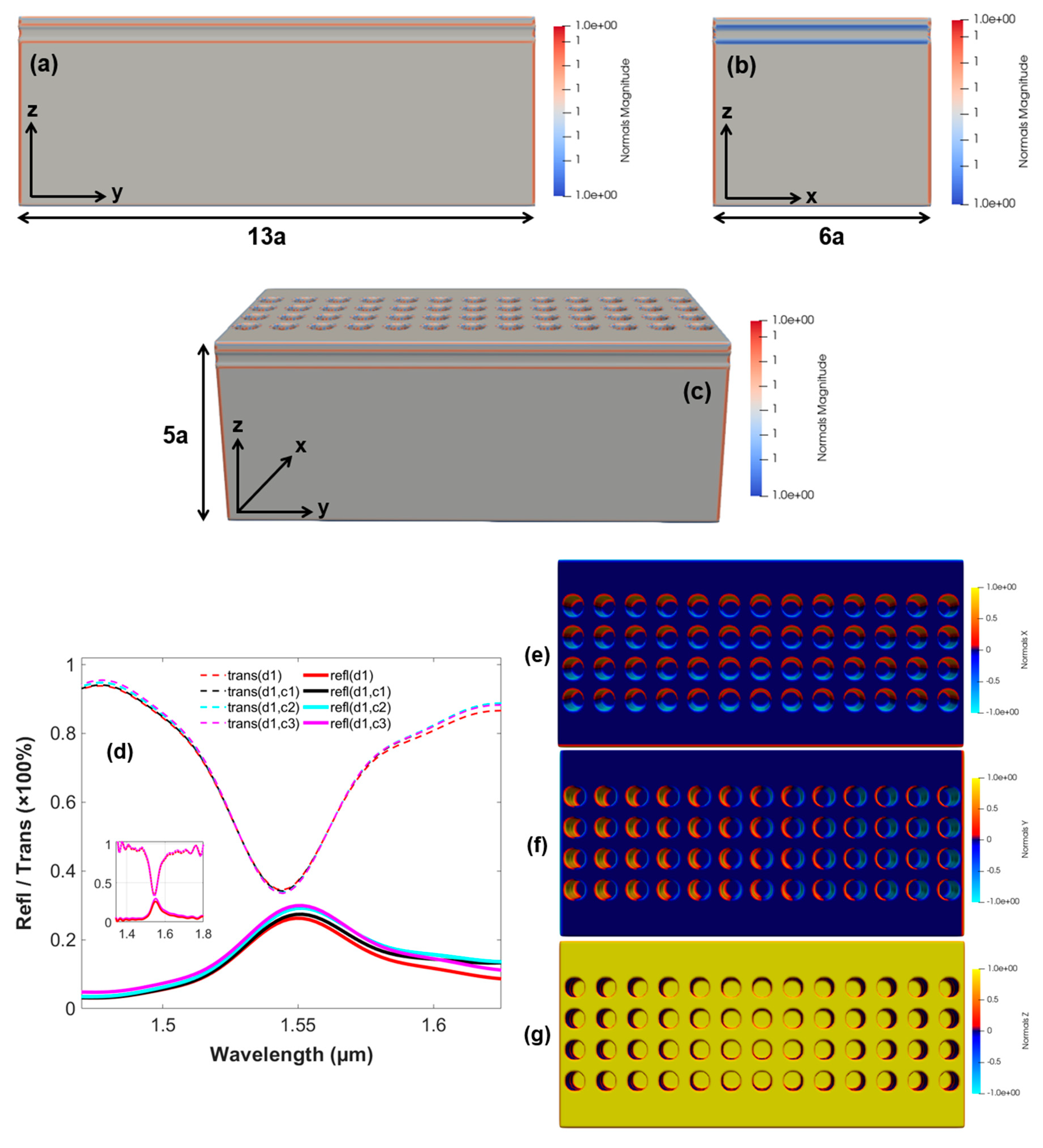
Similarly, the structure of the 3D optical switch based on the arrangement of the 4 PhC-elements, is imitated in
Figure 7(a-c), reporting the length, width, and height of the finite model respectively. Moreover, the optical switching action is shown in
Figure 7(d) using the reflection and transmission of the structure, using the control signal with a varying wavelength in the range i.e., 1.67µm-1.55µm along the data signal simultaneously. Therefore, it can be seen that increasing the units of PhC-elements, increases the confinement of the GMR modes and coupling of energy further into the optical device. However, the increase in the number of the PhC-elements (x-axis) reports adverse effects on the optical switching of the device. Therefore, number of the PhC-elements is limited to four according to this research. Moreover, to increase the coupling and confinement of the GMR modes, the number of the PhC-elements can be increased along (y-axis), which will result in the reduction of the compactness of the device. The field confinement by the structure along (x and y) directions is shown in
Figure 7(e-f), with
Figure 7(g) depicting the intensity of the data signal only, on the surface of the optical structure.
5. Discussion
The modeling of the 3D optical switch, is still an innovative idea, having qualities like compactness, ease of fabrication, and implementable in PICs. An optical switching idea proclaimed in [
25], uses a control signal for amplification of the data signal in various structures in terms of variable number of the PhC-elements. Moreover, the structure of the optical switch as presented in [
25] and [
26], uses 11 PhC-elements along with variable PhC cavity realized at the start of the PhC-mesh to modulate the GMR-modes. Apart from these, a variable PhC cavity and the outcomes of the control signal on the output of the data signal and tunning of the GMR modes respectively are modeled in [
27]. To achieve efficient optical switching, different PhC-elements-based structures are used. However, one common path is followed in all of these investigations i.e., using the 2D simulation domain. Apart from these, optical switching is reported in [
63], using the plasmonics characteristics of the graphene having a Si core-based waveguide. The refractive index of the graphene clad is varied with a low-intensity pulse, in contrast which modifies the characteristics of the device and as an outcome, the aspects of the optical switch are achieved.
Table 5, reports the details of the previous studies in comparison with the current research.
6. Proposed Fabrication process
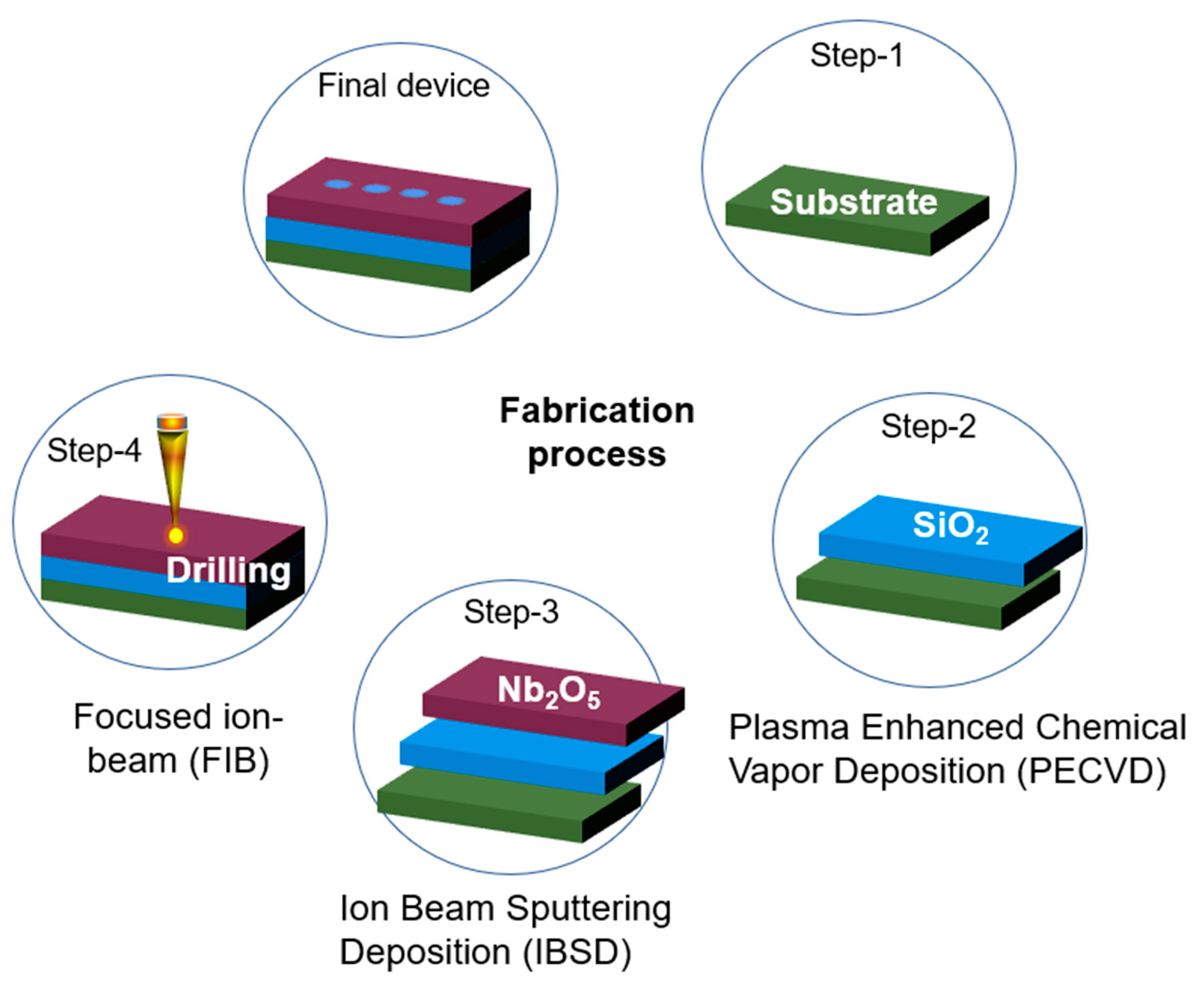
The proposed optical switching device can be realized using the conventional fabrication techniques used for optical integrated components as shown in
Figure 8. In the first step, Plasma Enhanced Chemical Vapor Deposition (PECVD) can be used for the deposition of the SiO
2 to form the base of the structure [
64]. In the second step, the waveguiding-layer i.e., Nb
2O
5 can be deposited over the layer of the SiO
2 using the method of Ion Beam Sputtering Deposition (IBSD) [
65]. In the last step, an array of PhC-elements can be structured using the Focused Ion-Beam (FIB) platform [
66].
7. Conclusions
In this study, a 3D-FDTD depiction of an optical switch is investigated. The switching action is studied utilizing two sources namely the data signal and the control signal in a dielectric slab-waveguide structure having an array of PhC-elements. The data signal is coupled into the device using GMR, which filters the data signal at the same time. While, the control signal is index guided into the optical structure, which is responsible for the optical switching and amplification of the data signal. The switching and amplification operation is fine-tuned by varying the central wavelength of the control and structural parameters of the device. The structural specifications of the device are optimized in terms of the radius and number of the periods of the PhCs i.e., 2 PhCs-elements and 4 PhC-elements (along x-axis). Likewise, two topologies are used i.e., structuring of the device using an infinite modeling mechanism, where a specific chunk of the device (along y-axis in this research) is repeated using the condition of PBC, to save time and computational resources. Secondly, a finite modeling mechanism, where a finite structure is concluded based on the results of the infinite structuring mechanism. Therefore, in the case of the arrangement comprising of 2 PhC-elements, produces pronounced effects of optical switching with high peaks in reflection spectra, narrow linewidth, and high-quality factor. However, it is not much effective in achieving the required resonant wavelength of the device. Similarly, implementing the 4 PhC-elements-based structure investigates lower coupling of energy having wider linewidth and decreased quality factor as compared to the 2 PhC-elements-based structure. The device can efficiently achieve optical switching at the desired wavelength range of 1.55µm. An amplification of about 13.75%, with a linewidth of 0.0079µm and a quality factor of 114.58 is attained. Considering the cases of the finite modeling, both of the arrangements i.e., 2 PhC-elements and 4 PhC-elements (along x-axis), reports the expected results of the infinite structuring mechanism. The design can be improved further by increasing the units of the PhC-elements (along the y-axis), which is limited by the computational resources in the meantime. The proposed design can be efficiently used in the fields of PICs, communications system, biomedical sensors and programmable photonics.
Author Contributions
Conceptualization, A.U.R., Y.K., M.I., S.C. and M.A.B.; methodology, A.U.R., Y.K., S.C. and M.A.B.; software, A.U.R., Y.K., S.C. and M.I.; validation, A.U.R., Y.K., M.I. and M.A.B.; formal analysis, A.U.R., Y.K., M.I., S.C. and M.A.B.; investigation, A.U.R., Y.K., M.I., S.C. and M.A.B.; resources, A.U.R., Y.K. and M.A.B.; data curation, A.U.R., N.L.K., Y.K., S.C. and M.A.B.; writing—original draft preparation, A.U.R., Y.K. and M.I.; writing—review and editing, A.U.R., Y.K., M.I., S.C. and M.A.B.; visualization, A.U.R., Y.K. and M.A.B.; supervision, Y.K., S.N.K., N.L.K. and M.A.B.; project administration, A.U.R., Y.K., S.N.K. and M.A.B.; funding acquisition, Y.K. and M.A.B. All authors have read and agreed to the published version of the manuscript.
Funding
The work was also carried out thanks to the funding of the Ministry of Education and Science of the Russian Federation of new laboratories under the guidance of young scientists within the framework of the national project "Science and Universities" (project FSSS-2021-0016) and under the FSRC “Crystallography and Photonics” of the Russian Academy of Sciences (the state task No. 007-GZ/Ch3363/26) in the overview comparative parts.
Institutional Review Board Statement
Not applicable.
Informed Consent Statement
Not applicable.
Data Availability Statement
Not applicable.
Acknowledgments
The authors would like to pay gratitude to Nanophotonics Research Group (BUITEMS), Quetta, and Parveen Ghoutie for their support and appreciation.
Conflicts of Interest
The authors declare no conflict of interest and agreed to the current version of the manuscript.
References
- Ono M, Hata M, Tsunekawa M, Nozaki K, Sumikura H, Chiba H, Notomi M. Ultrafast and energy-efficient all-optical switching with graphene-loaded deep-subwavelength plasmonic waveguides. Nature Photonics. 2020 Jan;14(1):37-43. [CrossRef]
- Sinatkas G, Christopoulos T, Tsilipakos O, Kriezis EE. Electro-optic modulation in integrated photonics. Journal of Applied Physics. 2021 Jul 7;130(1):010901. [CrossRef]
- Rao DG, Swarnakar S, Kumar S. Design of photonic crystal based compact all-optical 2× 1 multiplexer for optical processing devices. Microelectronics Journal. 2021 Jun 1; 112:105046. [CrossRef]
- Jiao S, Liu J, Zhang L, Yu F, Zuo G, Zhang J, Zhao F, Lin W, Shao L. All-optical logic gate computing for high-speed parallel information processing. Opto-Electronic Science. 2022 Sep 7;1(9):220010-1. [CrossRef]
- Rao DG, Swarnakar S, Palacharla V, Raju KS, Kumar S. Design of all-optical AND, OR, and XOR logic gates using photonic crystals for switching applications. Photonic Network Communications. 2021 Feb; 41:109-18. [CrossRef]
- Foroughifar A, Saghaei H, Veisi E. Design and analysis of a novel four-channel optical filter using ring resonators and line defects in photonic crystal microstructure. Optical and Quantum Electronics. 2021 Feb;53(2):101. [CrossRef]
- Miller, D.A.B. Are optical transistors the logical next step? Nature Photonics 2010, 4, 3–5.
- Safinezhad A, Babaei Ghoushji H, Shiri M, Rezaei MH. High-performance and ultrafast configurable all-optical photonic crystal logic gates based on interference effects. Optical and Quantum Electronics. 2021 May;53(5):259. [CrossRef]
- Liu C, Bai Y, Zhou J, Chen J, Qiao L. Refractive index sensing by asymmetric dielectric gratings with both bound states in the continuum and guided mode resonances. Optics Express. 2021 Dec 20;29(26):42978-88. [CrossRef]
- Royer F, Varghese B, Gamet E, Neveu S, Jourlin Y, Jamon D. Enhancement of both Faraday and Kerr effects with an all-dielectric grating based on a magneto-optical nanocomposite material. ACS omega. 2020 Feb 4;5(6):2886-92. [CrossRef]
- Mitrofanov AV, Sidorov-Biryukov DA, Rozhko MV, Voronin AA, Glek PB, Ryabchuk SV, Serebryannikov EE, Fedotov AB, Zheltikov AM. Relativistic nonlinear optical phenomena in the field of sub terawatt laser pulses. JETP Letters. 2020 Jul; 112:17-23.
- Raja-Mogan T, Ohtani B, Kowalska E. Photonic crystals for plasmonic photocatalysis. Catalysts. 2020 Jul 23;10(8):827. [CrossRef]
- Vigneron JP, Simonis P. Natural photonic crystals. Physica B: Condensed Matter. 2012 Oct 15;407(20):4032-6.
- Yablonovitch E. Photonic crystals. Journal of Modern Optics. 1994 Feb 1;41(2):173-94.
- Ahmed U, Khan Y, Ehsan MK, Amirzada MR, Ullah N, Khatri AR, Ur Rehman A, Butt MA. Investigation of spectral properties of dbr-based photonic crystal structure for optical filter application. Crystals. 2022 Mar 17;12(3):409. [CrossRef]
- Decleer, P.; Van Londersele, A.; Rogier, H.; Ginste, D.V. An alternating-direction hybrid implicit-explicit finite-difference time-domain method for the schrödinger equation. J. Comput. Appl. Math. 2022, 403, 113881. [CrossRef]
- Barabanova EA, Vytovtov KA, Nguyen TT. The control system elements of the new generation optical switching cell. Journal of Physics: Conference Series. 2019 Nov 1 (Vol. 1368, No. 2, p. 022002). IOP Publishing. [CrossRef]
- Yanik MF, Fan S, Soljačić M, Joannopoulos JD. All-optical transistor action with bistable switching in a photonic crystal cross-waveguide geometry. Optics letters. 2003 Dec 15;28(24):2506-8. [CrossRef]
- Nguyen HA, Grange T, Malik NS, Dupuy E, Tumanov D, de Assis PL, Yeo I, Fratini F, Gregersen N, Auffèves A, Gérard JM. Ultra-low power optical transistor using a single quantum dot embedded in a photonic wire. Quantum Information and Measurement. 2017 Apr 5 (pp. QT2B-2). Optica Publishing Group.
- Ma L, Li C, Sun L, Song Z, Lu Y, Li B. Submicrosecond electro-optical switching of one-dimensional soft photonic crystals. Photonics Research. 2022 Mar 1;10(3):786-92. [CrossRef]
- Ouahab I, Naoum R. A novel all optical 4× 2 encoder switch based on photonic crystal ring resonators. Optik. 2016 Oct 1;127(19):7835-41. [CrossRef]
- Brunetti G, Marocco G, Di Benedetto A, Giorgio A, Armenise MN, Ciminelli C. Design of a large bandwidth 2× 2 interferometric switching cells based on a sub-wavelength grating. Journal of Optics. 2021 Aug 20;23(8):085801. [CrossRef]
- Huang Y, Ho ST. Photonic Transistors based on Gain and Absorption Manipulation of Optical Interference. In 2007 Photonics in Switching 2007 Aug 19 (pp. 137-138).
- Ju S, Facchetti A, Xuan Y, Liu J, Ishikawa F, Ye P, Zhou C, Marks TJ, Janes DB. Fabrication of fully transparent nanowire transistors for transparent and flexible electronics. Nature nanotechnology. 2007 Jun;2(6):378-84. [CrossRef]
- Rehman AU, Khan Y, Irfan M, Butt MA, Khonina SN, Kazanskiy NL. A novel design of optical switch based on guided mode resonances in dielectric photonic crystal structures. Photonics. 2022 Aug 17 (Vol. 9, No. 8, p. 580). [CrossRef]
- Rehman AU, Khan Y, Fomchenkov S, Butt MA. Investigation of Optical Amplification Action in Dielectric Photonic Crystals Cavity Based Structure. In 2022 VIII International Conference on Information Technology and Nanotechnology (ITNT) 2022 May 23 (pp. 1-5).
- Rehman AU, Khan Y, Irfan M, Butt MA. Investigation of Optical-Switching Mechanism Using Guided Mode Resonances. Photonics. 2022 Dec 23 (Vol. 10, No. 1, p. 13). [CrossRef]
- Chhipa MK, Madhav BT, Suthar B. An all-optical ultracompact microring-resonator-based optical switch. Journal of Computational Electronics. 2021 Feb; 20:419-25. [CrossRef]
- Yu Y, Xue W, Hu H, Oxenløwe LK, Yvind K, Mork J. All-optical switching improvement using photonic-crystal Fano structures. IEEE Photonics Journal. 2016 Jan 28;8(2):1-8. [CrossRef]
- Bekele D, Yu Y, Yvind K, Mork J. In-Plane Photonic Crystal Devices Using Fano Resonances. Laser & Photonics Reviews. 2019 Dec;13(12):1900054. [CrossRef]
- Rajasekar R, Parameshwari K, Robinson S. Nano-optical switch based on photonic crystal ring resonator. Plasmonics. 2019 Dec; 14:1687-97. [CrossRef]
- Ghadrdan M, Mansouri-Birjandi MA. Implementation of all-optical switch based on nonlinear photonic crystal ring resonator with embedding metallic nanowires in the ring resonators. Optical and Quantum Electronics. 2016 May; 48:1-9. [CrossRef]
- Radhouene M, Najjar M, Chhipa MK, Robinson S, Suthar B. Design and analysis a thermo-optic switch based on photonic crystal ring resonator. Optik. 2018 Nov 1; 172:924-9. [CrossRef]
- Rajasekar R, Kumar KV, Ayyanar N, Raja GT. High Speed Optical Switch Based on Photonic Crystal Resonator. In 2020 IEEE 20th International Conference on Nanotechnology (IEEE-NANO) 2020 Jul 29 (pp. 295-298).
- Rostamizadeh A, Taghizadeh M, Jamali J, Andalib A. Ultra-fast all optical decoder using photonic crystal based nonlinear ring resonators. Optical and Quantum Electronics. 2020 Feb; 52:1-0. [CrossRef]
- Rebhi S, Najjar M. Hourglass nonlinear photonic crystal cavity for ultra-fast all-optical switching. Optik. 2019 Feb 1; 180:858-65. [CrossRef]
- Takiguchi M, Takemura N, Tateno K, Nozaki K, Sasaki S, Sergent S, Kuramochi E, Wasawo T, Yokoo A, Shinya A, Notomi M. All-optical switching using a III-V nanowire integrated Si photonic crystal nanocavity. In 2019 IEEE Photonics Conference (IPC) 2019 Sep 29 (pp. 1-2).
- Nozaki K, Tanabe T, Shinya A, Matsuo S, Sato T, Taniyama H, Notomi M. Sub-femtojoule all-optical switching using a photonic-crystal nanocavity. Nature Photonics. 2010 Jul;4(7):477-83. [CrossRef]
- Mehdizadeh F, Alipour-Banaei H, Serajmohammadi S. Study the role of non-linear resonant cavities in photonic crystal-based decoder switches. Journal of Modern Optics. 2017 Jul 20;64(13):1233-9. [CrossRef]
- Saudan Q, Bekele DA, Dong G, Yu Y, Yvind K, Mørk J, Galili M. Crosstalk-free all-optical switching enabled by Fano resonance in a multi-mode photonic crystal nanocavity. Optics Express. 2022 Feb 28;30(5):7457-66. [CrossRef]
- Shirdel M, Mansouri-Birjandi MA. Photonic crystal all-optical switch based on a nonlinear cavity. Optik. 2016 Apr 1;127(8):3955-8. [CrossRef]
- Asakawa K, Sugimoto Y, Watanabe Y, Ozaki N, Mizutani A, Takata Y, Kitagawa Y, Ishikawa H, Ikeda N, Awazu K, Wang X. Photonic crystal and quantum dot technologies for all-optical switch and logic device. New Journal of Physics. 2006 Sep 22;8(9):208. [CrossRef]
- Nakamura H, Sugimoto Y, Kanamoto K, Ikeda N, Tanaka Y, Nakamura Y, Ohkouchi S, Watanabe Y, Inoue K, Ishikawa H, Asakawa K. Ultra-fast photonic crystal/quantum dot all-optical switch for future photonic networks. Optics express. 2004 Dec 27;12(26):6606-14.
- Chen F. A tunable high-efficiency optical switch based on graphene coupled photonic crystal’s structure. Journal of Modern optics. 2017 Aug 22;64(15):1531-7. [CrossRef]
- Jalali Azizpour MR, Soroosh M, Dalvand N, Seifi-Kavian Y. All-optical ultra-fast graphene-photonic crystal switch. Crystals. 2019 Sep 3;9(9):461. doi:10.3390/cryst9090461.
- Zhang L, Sun Y, Li Z, Wang L, Cao S, Yang S, Wu Y, Tai R. Photonic crystal based on mott phase change material as all-optical bandgap switch and composite logic gate. Optical Materials. 2021 Mar 1; 113:110855. [CrossRef]
- Jiang M, Zhang D, Lian T, Wang L, Niu D, Chen C, Li Z, Wang X. On-chip integrated optical switch based on polymer waveguides. Optical Materials. 2019 Nov 1; 97:109386. [CrossRef]
- Mazurenko DA, Kerst R, Dijkhuis JI, Akimov AV, Golubev VG, Kurdyukov DA, Pevtsov AB, Sel’Kin AV. Ultrafast optical switching in three-dimensional photonic crystals. Physical review letters. 2003 Nov 19;91(21):213903.
- Meng ZM, Chen CB, Qin F. Theoretical investigation of integratable photonic crystal nanobeam all-optical switching with ultrafast response and ultralow switching energy. Journal of physics D: applied physics. 2020 Mar 19;53(20):205105. [CrossRef]
- Monfared SA, Seifouri M, Hamidi SM, Mohseni SM. Electro-optical switch based on one-dimensional graphene-plasmonic crystals. Optical Materials. 2021 May 1; 115:111051. [CrossRef]
- Zhao Y, Qian C, Qiu K, Gao Y, Xu X. Ultrafast optical switching using photonic molecules in photonic crystal waveguides. Optics express. 2015 Apr 6;23(7):9211-20. [CrossRef]
- Ma L, Li C, Sun L, Song Z, Lu Y, Li B. Submicrosecond electro-optical switching of one-dimensional soft photonic crystals. Photonics Research. 2022 Mar 1;10(3):786-92. [CrossRef]
- Qi H, Wang X, Hu X, Du Z, Yang J, Yu Z, Ding S, Chu S, Gong Q. All-optical switch based on novel physics effects. Journal of Applied Physics. 2021 Jun 7;129(21):210906. [CrossRef]
- Rajasekar R, Raja GT, Robinson S. Numerical investigation of reconfigurable photonic crystal switch based on phase change nanomaterial. IEEE Transactions on Nanotechnology. 2020 Jun 17; 19:545-52. [CrossRef]
- Takiguchi M, Takemura N, Tateno K, Nozaki K, Sasaki S, Sergent S, Kuramochi E, Wasawo T, Yokoo A, Shinya A, Notomi M. All-optical InAsP/InP nanowire switches integrated in a Si photonic crystal. ACS Photonics. 2020 Mar 9;7(4):1016-21. [CrossRef]
- Tanabe T, Taniyama H, Notomi M. Carrier diffusion and recombination in photonic crystal nanocavity optical switches. Journal of Lightwave Technology. 2008 Jun 13;26(11):1396-403.
- Plander I, Stepanovsky M. MEMS optical switch: Switching time reduction. Open Computer Science. 2016 Jan 1;6(1):116-25. [CrossRef]
- MEEP Documentation MkDocs. Available online: https://meep.readthedocs.io/en/latest/ (accessed on 14 April 2022).
- Oskooi, A.F.; Roundy, D.; Ibanescu, M.; Bermel, P.; Joannopoulos, J.D.; Johnson, S.G. A flexible free-software package for electromagnetic simulations by the fdtd method. Comput. Phys. Commun. 2010, 181, 687–702. [CrossRef]
- Yee, K.S. Numerical solution of initial boundary value problems involving maxwell’s equations in isotropic media. IEEE Trans. Antennas Propag. 1966, 14, 302–307. [CrossRef]
- Khan, Y.; Butt, M.A.; Kazanskiy, N.L.; Khonina, S.N. numerical study of fabrication-related effects of the structural-profile on the performance of a dielectric photonic crystal-based fluid sensor. Materials 2022, 15, 3277. [CrossRef]
- Khan, Y. Design and Numerical Simulation of Dielectric Photonic Crystal Devices and Investigation of an Optical Characterization Method. Ph.D. Thesis, University of Kassel, Kassel, Germany, 2017.
- Sahu PP. Optical switch based on graphene clad two surface plasmonic polariton mode coupler. Optik. 2021 Feb 1; 227:166026. [CrossRef]
- Okada H, Baba M, Furukawa M, Yamane K, Sekiguchi H, Wakahara A. Formation of SiO2 film by chemical vapor deposition enhanced by atomic species extracted from a surface-wave generated plasma. In AIP Conference Proceedings 2017 Jan 26 (Vol. 1807, No. 1, p. 020006).
- Becker M, Benz SL, Chen L, Polity A, Klar PJ, Chatterjee S. Controlled thin-film deposition of α or β Ga2O3 by ion-beam sputtering. Journal of Vacuum Science & Technology A: Vacuum, Surfaces, and Films. 2020 Dec 5;38(6):063412.
- Li W, van Baren J, Berges A, Bekyarova E, Lui CH, Bardeen CJ. Shaping organic microcrystals using focused ion beam milling. Crystal Growth & Design. 2020 Feb 6;20(3):1583-9. [CrossRef]
Figure 1.
(a) Photonic integrated circuit (b) Conceptual diagram of the 3D optical switch.
Figure 1.
(a) Photonic integrated circuit (b) Conceptual diagram of the 3D optical switch.
Figure 2.
Infinite structures of the 3-D optical switch (a) The view of the 3-D optical switch along (x-axis) showing the data signal, reflection and transmission monitoring layers, and field decay monitor point. (b) Cross-section view along (y-axis). (c) Top view along (x-axis). (d) A unit cell of the device shows the direction of the control signal.
Figure 3.
(a) The output reflection spectra of the infinite models of the 3D optical switch comprising of 2 and 4 PhC-elements (along the x-axis) respectively. (b) Electric field confinement by 2 PhC-elements-based structure (c) Electric field confinement by 4 PhC-elements-based structure. (d) Magnetic field confinement by 2 PhC-elements-based structure. (e) Magnetic field confinement by 4 PhC-elements-based structure.
Figure 4.
(a) Output reflection spectra of the data signal relating to infinite model of the 2 PhC-elements-based structure investigating the phenomenon of optical switching concerning varying wavelength of the control signal (b) Linewidth (c) Quality factor .
Figure 4.
(a) Output reflection spectra of the data signal relating to infinite model of the 2 PhC-elements-based structure investigating the phenomenon of optical switching concerning varying wavelength of the control signal (b) Linewidth (c) Quality factor .
Figure 5.
(a) Output reflection spectra of the data signal relating to infinite model of the 4 PhC-elements-based structure investigating the phenomenon of optical switching w.r.t varying wavelength of the control signal (b) Linewidth (c) Quality factor.
Figure 5.
(a) Output reflection spectra of the data signal relating to infinite model of the 4 PhC-elements-based structure investigating the phenomenon of optical switching w.r.t varying wavelength of the control signal (b) Linewidth (c) Quality factor.
Figure 6.
Finite model of the 3-D optical switch comprising of the 2 PhC-elements along (x-axis) (a) Lateral view of the optical switch along (y-axis) (b) Cross-sectional view along (x-axis) (c) Finite model representation along (x, y, z) directions (d) Output reflection and transmission spectra of the finite model signifying the properties of optical switching (e) Field confinement (x-axis) (f) Field confinement (y-axis) (g) Intensity of data signal on the surface of the optical switch (z-axis). .
Figure 7.
Finite model of the 3-D optical switch comprising of the 4 PhC-elements along (x-axis) (a) Lateral view of the optical switch along (y-axis) (b) Cross-sectional view along (x-axis) (c) Finite model representation along (x, y, z) directions (d) Output reflection and transmission spectra of the finite model signifying the properties of optical switching (e) Field confinement (x-axis) (f) Field confinement (y-axis) (g) Intensity of data signal on the surface of the optical switch (z-axis).
Figure 8.
The stepwise fabrication-process of the reported optical switching device. .
Figure 8.
The stepwise fabrication-process of the reported optical switching device. .
Table 1.
Augmented parameters of the 3D optical switch.
Table 1.
Augmented parameters of the 3D optical switch.
| Parameters |
Symbol |
Value |
| Lattice-constant |
a |
1µm |
| Radius of PhC-elements |
r |
0.300a |
| Thickness of waveguides |
wthick
|
0.330a |
| Thickness of cladding |
- |
0.300a |
| Thickness of Perfectly Matched Layer |
PML |
3.0a, (along x and z) axes |
| Refractive index of the substrate |
nsub
|
1.5 |
| Refractive index of the waveguide |
nwav
|
2.2 |
| Field decay monitor point |
- |
1 e -3
|
| Padding |
Padd
|
2.0a |
| Periodic Boundary Condition |
PBC |
Along y-axis |
| Resolution |
- |
20 |
| Smoothing factor |
- |
0.05 |
| Grid size |
- |
0.52 |
Table 2.
Properties are achieved by the infinite models of the 3-D optical switch comprising of the 2 and 4 PhC-elements, respectively.
Table 2.
Properties are achieved by the infinite models of the 3-D optical switch comprising of the 2 and 4 PhC-elements, respectively.
| Number of PhC-Elements |
Resonant Wavelength (µm) |
Reflection Peak (%) |
Linewidth
(µm) |
Quality Factor
- |
| 2 PhC-elements |
1.528 |
81.13 |
0.0204 |
39.76 |
| 4 PhC-elements |
1.547 |
71.43 |
0.0266 |
26.85 |
Table 3.
The table presents the names and differences in wavelengths of the data and control signal.
Table 3.
The table presents the names and differences in wavelengths of the data and control signal.
Type of Source
|
Name of Source |
| d1 |
c1 |
c2 |
c3 |
| Data signal |
1.55µm |
- |
- |
- |
| Control signal |
- |
1.67µm |
1.60µm |
1.55µm |
Table 4.
A detailed comparison between the infinite models of the 3-D optical switch based on 2 and 4 PhC-elements respectively.
Table 4.
A detailed comparison between the infinite models of the 3-D optical switch based on 2 and 4 PhC-elements respectively.
| 2 PhC-elements |
| Sources |
d1 |
c1 |
c2 |
c3 |
| Wavelength (µm) |
1.528 |
1.528 |
1.528 |
1.528 |
| Reflection (×100%) |
0.8113 |
0.8434 |
0.9052 |
0.9488 |
| Linewidth (µm) |
0.0204 |
0.0150 |
0.0079 |
0.0214 |
| Quality Factor |
39.77 |
56.23 |
114.58 |
44.34 |
| 4 PhC-elements |
| Sources |
d1 |
c1 |
c2 |
c3 |
| Wavelength (µm) |
1.547 |
1.547 |
1.547 |
1.547 |
| Reflection (×100%) |
0.7143 |
0.7343 |
0.7623 |
0.7741 |
| Linewidth (µm) |
0.0266 |
0.0149 |
0.0276 |
0.0269 |
| Quality Factor |
26.85 |
49.28 |
27.62 |
28.78 |
Table 5.
Comparison of the previous research studies with the current investigation of the optical switch.
Table 5.
Comparison of the previous research studies with the current investigation of the optical switch.
| Design |
Simulation Domain |
Linewidth (
µm)
|
Quality Factor
-
|
Research Work |
| SiO2 + Nb2O5 + SiO2 + PhCs (air) |
2D |
0.0696 |
- |
[25] |
| SiO2 + Nb2O5 + SiO2 + PhCs (air) |
2D |
0.0727 |
- |
[26] |
| SiO2 + Nb2O5 + SiO2 + PhCs (air) |
2D |
0.0652 |
12.96 |
[27] |
| SiO2 + Nb2O5 + SiO2 + PhCs (air) |
3D |
0.0079 |
114.58 |
This work |
|
Disclaimer/Publisher’s Note: The statements, opinions and data contained in all publications are solely those of the individual author(s) and contributor(s) and not of MDPI and/or the editor(s). MDPI and/or the editor(s) disclaim responsibility for any injury to people or property resulting from any ideas, methods, instructions or products referred to in the content. |
© 2023 by the authors. Licensee MDPI, Basel, Switzerland. This article is an open access article distributed under the terms and conditions of the Creative Commons Attribution (CC BY) license (http://creativecommons.org/licenses/by/4.0/).
