
You are currently viewing a beta version of our website. If you spot anything unusual, kindly let us know.
Preprint
Review
Research Progress on Metal-Organic Frameworks by Advanced Transmission Electron Microscopy
Altmetrics
Downloads
263
Views
110
Comments
0
A peer-reviewed article of this preprint also exists.


This version is not peer-reviewed
Abstract
Metal-organic frameworks (MOFs), composed of metal nodes and inorganic linkers are promising for a wide range of applications due to their unique periodic frameworks that can be flexibly tuned. Understanding of the structure-activity relationships can facilitate the development and application of MOFs nanomaterials. Transmission electron microscopy (TEM) is a one-of-a-kind technique capable of characterizing MOFs microstructures at the atomic scale. Besides, in-situ TEM set-ups make it possible to direct visualize the microstructural evolution of MOFs in real time, which enables monitoring transitions of MOFs during growth as well as under working conditions. However, MOFs are so sensitive to the high-energy electron beam which makes TEM-based characterizing methods challenging. In this review, we first introduce the main damage mechanisms for MOFs under electron beam irradiation and two strategies to minimize the damages: low-dose TEM and cryo-TEM. Then, we discuss the techniques combined with the two strategies to analyze the MOFs’ microstructure, including three-dimensional electron diffraction, direct detection electron counting camera, and iDPC-STEM. Groundbreaking milestones and research advances with respect to static characterization of MOFs structures are highlighted. In-situ TEM studies are exemplary reviewed to provide insights into MOFs dynamics induced by various stimuli. Additionally, perspectives on promising techniques that may further facilitate the MOFs study using TEM are analyzed.
Keywords:
Subject: Chemistry and Materials Science - Materials Science and Technology
1. Introduction
Metal-organic frameworks (MOFs) are porous crystalline materials comprised of inorganic metal ions or clusters and organic ligands [1]. As a unique class of materials featuring tunable topologies, large specific surface area, high porosity, adjustable chemical compositions, and functionalities, MOFs are promising candidates for catalysis [2], gas storage and separation [3,4], energy storage and conversion [5], chemical sensing [6], water adsorption [7], and lithium-ion storage [8], etc. Structure-activity relationships guide rational development and applications of flexible and functional MOFs. The determination at the atomic scale of the crystal structures and the mechanisms of structural evolution under realistic working conditions is a well-founded prerequisite for understanding the relationships.
Surface, interface, defect, and host-guest interaction are the main microstructures, which affect directly the MOFs’ properties. Considering practical applications, modification of surface is an important means of MOFs’ functionalization [9]. Surfaces have an impact on surface-related properties and growth processes [10]. Interfaces are of great significance between MOFs crystals or with other materials for plasma crystals, composites, MOF-based devices, among others [11-13]. Defects provide a method to locally adjust porosity and create active open metal sites for MOFs [14,15], which allows defect engineering for the specific function [16]. Defects can be introduced artificially under control for modifications [17], or be generated spontaneously during the assembly process [18]. Due to distinguished porous nature and long-distance orderly structure, MOFs crystals with interconnected rigid networks are ideal framework materials to provide regular and regionally large accommodations for guest species including ions, particles, clusters, and molecules [19-21]. Host-guest controllable incorporation and synergetic interactions allow for their applications [22,23]. To enhance the utilizations MOFs, thorough understanding of the growth and transformation mechanisms, as well as the evolution pathways of MOFs under working conditions are crucial in addition to the inherent properties of the static structure.
Among characterization techniques, transmission electron microscopy (TEM) is undoubtedly suitable, given the ability of high-energy electrons to interact with thin specimens. Apart from structural analysis via electron diffraction, both TEM mode and scanning transmission electron microscopy (STEM) mode permit direct imaging regions of interest in the specimen, including its periodic, non-periodic, local, and porous details inside and on the surface of MOFs at the atomic scale. Meanwhile, TEM is capable to be combined with spectroscopic techniques to examine the chemical elements. Moreover, using novel in-situ sample holders, TEM can introduce real-time external fields and conditions such as low temperature, heating, biasing, liquids, gases, etc., enabling on-demand scenarios of the sample in practical applications.
However, MOFs are difficult to stabilize under the high-energy electron beams due to their organic components and the coordination bonds that connect organic parts to the metals. The fundamental hinderance to analyzing MOFs using TEM is their extreme sensitivity to electron beam irradiation, which causes either the structural disintegration before detection finishing or the lack of intrinsic characteristics during acquisition [24,25]. Hence, the nature of MOFs weakens the feasibility and merits of research using TEM. It is essential to update TEM-related methods and techniques to be appropriate to beam-sensitive materials. To this end, the idea of low electron dose and low temperature was established for the consideration of damage mechanisms in MOFs [26,27]. Multiple advanced TEM techniques were developed, which primarily include three-dimensional electron diffraction (3DED), direct detection electron counting (DDEC) camera, and integrated differential phase-contrast scanning transmission electron microscopy (iDPC-STEM) imaging [28-30].
Several review articles have discussed the works on studying MOFs using TEM. Huang et al. summarized the development of 3DED methods and demonstrated their capabilities for MOFs’ structural characterization [31,32]. Wiktor et al. [33] and Liu et al. [34] presented the problems and approaches of MOFs’ research by TEM, and the advances in terms of structural characterization of MOFs up to that time. Apart from these aspects, Gong et al. [35] and Zhang et al. [36] discussed new findings based on in-situ TEM methods afterwards. Nevertheless, no articles have comprehensively proposed the scope of applicability of diverse TEM-related techniques for probing MOFs materials from the perspective of the theoretical principles and practical operations. Herein, we discuss the challenges, strategies, and advanced techniques for MOFs research based on TEM, and introduce representative research advances in structural analysis and dynamic evolution. We demonstrate the practicability and indispensability of TEM as a powerful tool in this field. Meanwhile, some perspectives on cutting-edge TEM-based techniques which are potential for MOFs study have been proposed.
2. Challenges and chances of TEM studies
MOFs are so unstable and sensitive to the high-energy electron beam featured in TEM, which makes the structural characterization of MOFs challenging. This necessitates knowledge of the electron beam damage mechanisms in MOFs.
2.1. Damage mechanisms
Radiation damage mechanisms of MOFs under the high-energy incident electron beam mainly include radiolysis, knock-on damage, and thermal effects [25]. In practical situations, the determination of the predominant mechanism can help find the proper method to minimize damage [24].
The radiolysis (or ionization damage) is electron-electron interaction-induced ionization of specimen atoms via inelastic scattering that results in chemical bond weakening or breakage, phonon scattering, etc. It is the primary cause of MOFs degradation as reported, especially at lower voltages. This beam damage can be eased by high-energy incident electrons because they lead to fewer inelastic scattering events. However, the signal-to-noise ratio of image and spectrum is unimproved because both the inelastic and elastic cross-sections are inversely proportional to incident energy [37]. Low temperature effectively improves the beam stability of the specimen and mitigate radiolysis, which can be realized at cryogenic temperatures by using liquid nitrogen or helium (cryo-TEM) [24,27].
The knock-on damage originates from direct electron-nucleus interaction, specifically the atomic displacements or sputtering in the original specimen caused by high-energy electrons. Low-energy incident electrons prevent knock-on damage, whereas at the cost of weak beam penetration depth and poor signal resolution[25]. Reduction of the TEM accelerating voltage below the sample-specific threshold value while maintaining the resolution (low-voltage TEM) is an alleviation method.
The thermal effects (or beam heating) arise from electron-atom interaction-induced collective crystal lattice vibration, and can be mitigated by lowering the incident-beam current [37]. This damage can be mitigated to some extent by cryogenic temperatures.
2.2. Strategies for minimizing damages
Principles for structural maintenance when probing the static structure and dynamic behavior of MOFs by TEM without damaging the intrinsic properties can be broadly divided into two parts: low-dose TEM and cryo-TEM.
2.2.1. Low-dose TEM
Given that all these electron beam-induced irradiation damages are dose-related, reduction of the electron dose (low-dose TEM) is a general solution applied to MOFs regardless of the damage mechanism. A pre-evaluation is required to determine whether the low-dose conditions are within the acceptable range to maintain the stability of crystallinity. Electron diffraction (ED) is an effective and feasible way to determine the electron dose that the MOF can withstand, partly because it can be performed at low doses. As the electron dose increases, changes in the ED patterns mean modifications in the structure, i.e., the appearance of disordered phases. Shorter exposure time and lower intensity contribute to achieving low electron dose conditions [26]. The maximal electron dose that MOFs can withstand depends on materials and respective TEM operating conditions. Take typical MOFs in TEM mode under 300 kV accelerated electron beam as examples, the electron dose that MIL-101(Cr) can withstand is ~16 e- Å-2 [40]. The onset of beam damage for UiO-66(Zr) was from 10 to 20 e- Å-2 [25], and ZIF-8(Zn) about 25 e- Å-2 [41]. Compared to static characterization, in-situ TEM studies require longer irradiation time, which necessitates an electron dose considerably below the damage threshold to ensure the integrity of the sample region of interest during dynamic processes. In the liquid cell TEM (LCTEM) observations of UiO-66(Zr) and ZIF-8(Zn), the cumulative electron flux of ~20 times less than the threshold was considered appropriate [42].
2.2.2. Cryo-TEM
Cryo (low-temperature) concepts can be introduced to MOFs to probe structural details without collapse because they are able to preserve the native state and extend the irradiation time span, although there is a limit to the reduction of degradation caused by heating [25,27]. For example, at 120 K, the structures of the highly porous CAU-7(Bi) were characterized by ED [43]. At liquid nitrogen temperature, the complete pore structure and the periodicity of the crystal lattice of MOF-5(Zn) nanocrystals were imaged by high-resolution TEM (HRTEM) [27]. Cryogenic temperatures also enable the elucidation of the orderly internal architecture of large-area conductive 2D Cu2(TCPP) (TCPP = meso-tetra(4-carboxyphenyl)porphine) films on dielectric substrates by HRTEM and ED [44].
Apart from minimizing structural damage and improving electron tolerance during characterization, cryo-TEM also helps stabilize and preserve specimens at the status of interest during an in-situ TEM observation. Examples include in-situ studies on the crystallinity of MOFs in the liquid phase at specific reaction stages [45,46] and the construction of MOFs after interaction with gas species [47]. For the latter, two preferred adsorption sites for CO2 were discovered to be the centers within 6-ring channels and 4-ring channels, supported by HRTEM performed at -170 °C and with a cumulative electron flux of ~7 e- Å-2 using a DDEC camera. The unit cell of ZIF-8(Zn) expanded by ~3% due to molecular guests (Figure 1a–d) [47].
In addition, cryogenic conditions are applicable to the biological field, such as biomacromolecule-metal-organic frameworks (biomacromolecule-MOFs). For protein-ZIF-8(Zn), the amorphous precursor phase in the nucleation was directly observed, revealing a non-classical nucleation approach of dissolution-recrystallization and protein-rich amorphous solid phase transformation [48]. Furthermore, under cryogenic settings, the difference in atomic-level nanoarchitectures, which significantly affected the bioactivity and was caused by different crystallization pathways in synthetic scenarios, was unraveled for the first time. For BZIF-8-S, heterogeneously crystallized by solid-state transformation of the biomacromolecule amorphous phase at the spontaneously growing ZIF-8 crystal surface, the crystal structure with regularly narrow pore windows hindered the diffusion of the catalytic substrate. For BZIF-8-B, crystallized around surface directly via electrostatic interaction with the induction of biomacromolecules, slow crystallization rate with an observable amorphous phase as well as defects enhanced the bioactivity (Figure 1e–g) [49].
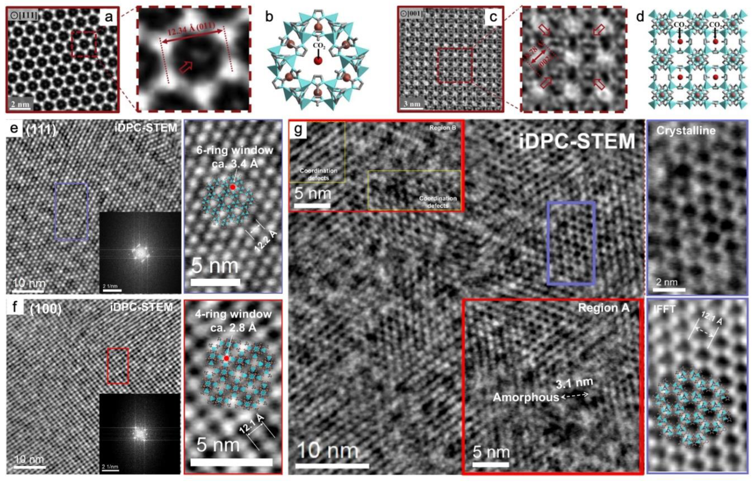
Figure 1.
HRTEM characterization under cryogenic conditions of CO2@ZIF-8(Zn)[47] and protein-ZIF-8(Zn) composites[49]. (a-d) Host-Guest Structures within ZIF-8(Zn) viewed along [111] (a, b) and [001] (c, d) projection. (a, c) Left: CTF-corrected Cryo-TEM images of CO2-filled ZIF-8 particle taken with electron dose rate of ∼4.5 e- Å-2 s-1 for 1.5 s. Bright regions correspond to mass density, and contrast in the center of the 6-ring window (a) and 4-ring window (c) is observed respectively for multiple unit cells. Middle: magnified image of a single ZIF-8-unit cell. Density at the center indicated by red arrows likely corresponds to CO2 adsorbed within ZIF-8. In (c), only the pore cavity at the vertices of the 4-ring window contains this density. (b, d) Simulated structure of ZIF-8 with DFT-predicted binding site of CO2 indicated with red spheres in (a, c), respectively[47]. (e-g) iDPC-STEM images, corresponding FFT, and the structural analysis of the selected area (indicated with the same color) of BZIF-8-S from the [111] (e) and [100] (f), and BZIF-8-B from the [111] (g) zone axis. (e, f) show high-crystallinity with ~3.4 Å 6-ring window and ~2.8 Å 4-ring window, respectively. (g) shows crystalline and amorphous phase, and coordination defects[49].
3. Strategies, techniques, and research advances
3.1. Traditional and Advanced electron diffraction
Large MOF crystals are occasionally difficult to prepare, and frequently, only nano- or submicron-sized crystals can be manufactured based on reaction kinetics and thermodynamics. Electron diffraction (ED), because of its ability to probe nanosized crystals, is better suited for structural investigations of MOFs than conventional X-ray diffraction (XRD) which is ideal for atomic-scale analysis of large crystals (at least microns in size) [50]. ED is preferable to HRTEM because it requires a lower dose of electrons to achieve the same level of resolution, if the resolution and observed region meet the practical requirements. This supports the use of ED to determine the maximum amount of electron flux that MOFs can withstand. For instance, ED reviewed ZIF-8(Zn) crystals with enough contrast at a dose rate of only ~1 e- Å-2 s-1 [41]. ED requires tilting the crystal along specific zone axes in order to obtain accurate structural information. However, beam-sensitive MOFs suffer from the time-consuming process of collecting a few ED patterns along precisely aligned crystallographic zone axes. The challenge of accurately describing the crystal structure by ED also lies in the method of merging multiple ED maps, which requires the correct handling of multiple scattering effects [51]. Therefore, the limitations are primarily related to the data collection strategy.
Three-dimensional electron diffraction (3DED) enables the effective collection of ED data and subsequent ab initio structure determination and analysis [28]. The 3DED data set of a single crystal is a sequence of ED patterns recorded sequentially at different tilt angles of the TEM goniometer, which then produce corresponding diffraction peaks (Figure 2a) [32]. This technique so far has evolved from stepwise strategies to the faster continuous strategies from a data collection perspective.
Among the former type, electron diffraction tomography (EDT) was first proposed in the late 2000s [52]. The program-controlled TEM sample stage automatically records the stepwise tilt angle relative to the electron beam and collects the rotational motion of the ED patterns. Apart from MOFs themselves, the EDT technique has also been applied to the distribution of guests in MOFs, such as TiO2 in MIL-101(Cr) mesopores [53]. To decrease the required electron beam intensity, automatic diffraction tomography (ADT) combined with precession electron diffraction (PED) equipment was designed later to control tilt angles of goniometers. This protocol improves the analysis of porous and organic sub-microcrystalline samples at the single-crystal scale, but operate entirely in STEM mode [52,54,55]. Using ADT and a cryo-TEM holder, bismuth-based MOF Bi(BTB) (BTB=1,3,5-benzenetrisbenzoate) (also denoted as CAU-7) was reconstructed, and the law of triple twinning of pseudo-hexagonal symmetry growth of the rod-shaped aggregates was proposed.[43]. Compared to the PED method, which is suitable for the near-kinematical data collection from single zone axes, rotational electron diffraction (RED) contributes to the complete collection of 3DED data and reconstructs the reciprocal space with high resolution [56]. In addition to the goniometer tilt controlled by ADT, RED combines fine electron beam tilt so as to further accelerate data collection and eliminate the need for precise alignment to specific zone axes. RED assisted in the direct determination of the pore structure of UiO-66(Zr), which was further confirmed by Rietveld refinement of XRD [50].
The latter type of strategy enables crystals to be rotated continuously to speed up data acquisition and simultaneously obtain relatively accurate and complete ED intensities as a movie. This type improves on the previous one by limiting the goniometer tilt and is particularly suitable for crystals with low symmetry. Continuous rotation electron diffraction (cRED) has elucidated structures of several types of MOFs and has always been confirmed or supplemented by relatively ambiguous XRD data in reported works. Examples include atomic positions of Ti8Zr2O12(COO)16 cluster-based PCN-415 and PCN-416 [57], and lattice of TiVI 4,4’-biphenyldicarboxylate (bpdc2-) MOF termed COK-47 [58], Zr chain-based PCN-226 [59], ZIF-EC1(Zn, Co) [60]. UU-100(Co) was unraveled to have a tetrahedral unit cell with the lattice parameters a = b = 27.3 Å and c = 19.6 Å, a possible P4/mbm space group, and rectangular channels with elliptical pores [61]. Despite the current rarity of high conductivity in MOFs, MOFs are welcomed in fields such as electrocatalysis and charge storage because of their porous structures [62]. Electrically conductive 2D MOFs have attracted attention for their hexagonal 2D lattices like 2D van der Waals stacked materials. In regard to a class of 2D π-conjugated MOFs, the structure details of M3HHTT2 (HHTT = 2,3,7,8,12,13-hexahydroxy tetraazanaphthotetraphene, M = Cu2+ or Ni2+) with a resolution of ~1.5 Å verified convincingly the π-stacking by an interlayer distance of 3.19±0.02 Å, which results in rare eclipsed AA stacking [63]. Crystal tracking was developed to resolve the issue of likely divergence of crystals from the selected regions during continuous rotation by defocusing every few ED patterns [64]. Micro-electron diffraction (MicroED) is a technique that uses an ultra-low electron dose at cryogenic temperatures and is similar in principle to PED [65,66]. It has been extended from biomacromolecules to the beam-sensitive materials, as exemplified by the structure of ZIF-8(Zn), which was determined to be 0.87 Å from a single nanocrystal and compares well with XRD results [67]. Notably, the environmental 3DED method in combination with continuous 3DED and environmental TEM (ETEM) has been proposed and validated for single microcrystals to study the structural dynamics under external stimuli. The atomic-level ab initio structure determination of MIL-53(Al) under vacuum, cryo, heating, gas, and liquid conditions was conducted (Figure 2c) [68]. Thus, it was demonstrated that in-situ ED, as an in-situ TEM-based approach, can also be used to analyze the dynamic behaviors of MOFs placed in external fields [68].
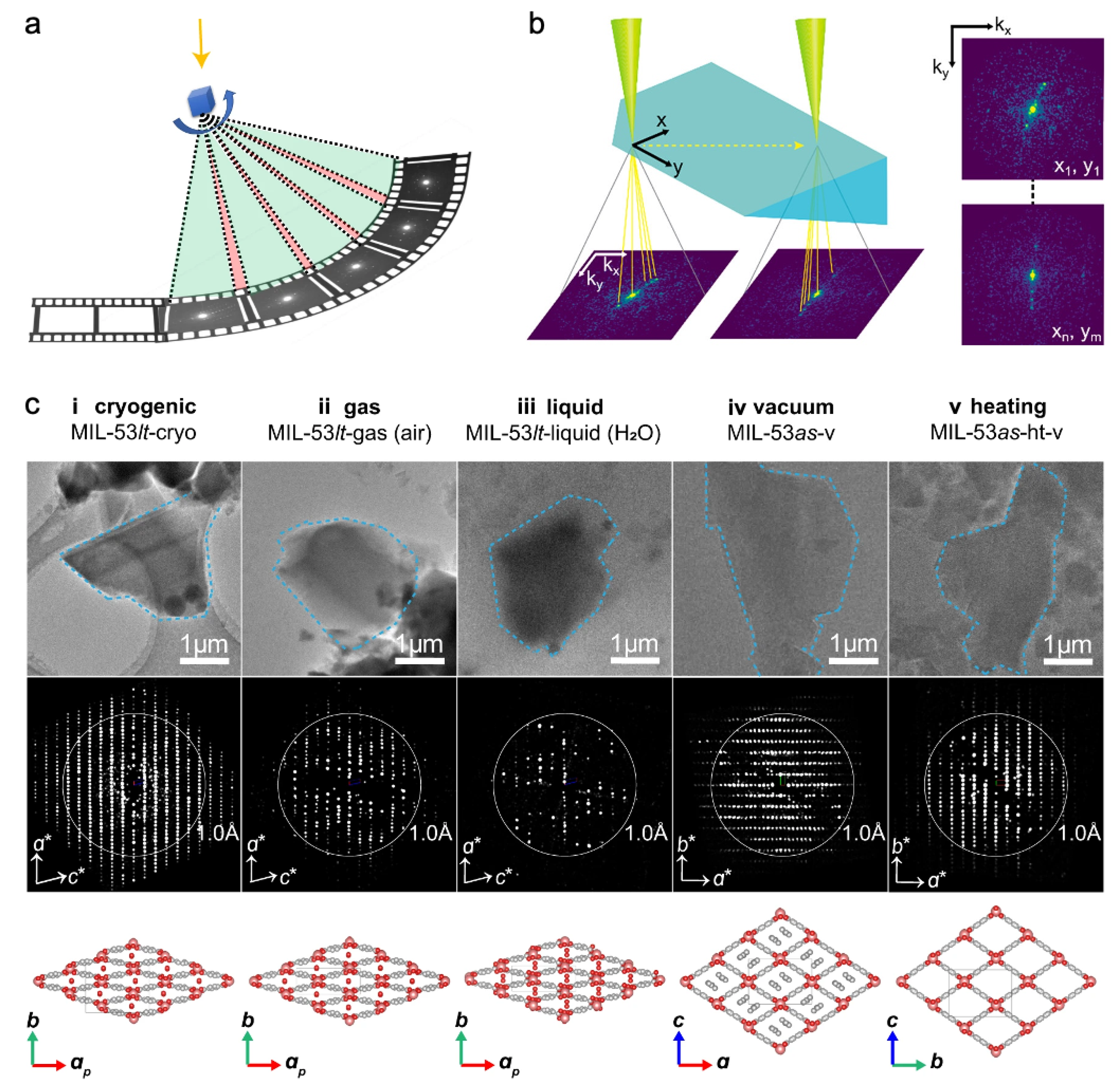
Figure 2.
Advanced electron diffraction: three-dimensional electron diffraction (3DED)[32,68] and scanning electron diffraction (SED)[15]. (a) The data collection procedure of 3DED. Green: obtained data; pink: missing wedges; blue cube: target crystal; blue arrow: rotation direction; yellow arrow: incident electron beam[32]. (b) Illustration of SED applied to a defect-engineered UiO-66(Hf) particle. A 2D (kx, ky) diffraction pattern is recorded in transmission at every probe position in a 2D (x, y) scan[15]. (c) ETEM images (top), ETEM 3DED data (middle), and determined structures (bottom) of MIL-53(Al) single crystals under different conditions. Particles marked with blue dashed lines (top) were used for collecting 3DED data. White circles in diffraction data (bottom) represent a resolution of 1 Å. The 3DED data are projected along the [010] (i-iii) and [001] (iv, v) directions of the samples: the as-made phase (MIL-53as), the high-temperature phase (MIL-53ht) and the H2O-containing phase (MIL-53lt, room temperature, in the air). (i) MIL-53lt-cryo: the low temperature phase prepared by plunge-freezing and cryogenic transfer protocols. (ii) MIL-53lt-gas (air): MIL-53lt in the static air (0.1 MPa). (iii) MIL-53lt-liquid (H2O): MIL-53lt covered with liquid water. (iv) MIL-53as-v: the as-synthesized phase MIL-53as under high vacuum state. (v) MIL-53as-ht-v: the phase after calcination of MIL-53as at 603 K and high vacuum for 2 h[68].
Conventionally, ED is only applicable to reveal spatial average information, including periodic crystal structures or abnormal macroscopic features. It is represented by revealing the reo topology with the existence of missing cluster defects of UiO-66(Hf) via multiple diffraction behaviors, including ED [17]. Direct imaging methods in TEM mode or STEM mode are always required to resolve local non-periodic structures such as surfaces, interfaces, defects, guest molecules, etc., which are equally important. Organic molecules in pores were for the first time located using cRED with a resolution of 0.83-1.00 Å, in the study of Co2(Ni-H4TPPP)]·2DABCO·6H2O (DABCO = 1,4-diazabicyclo[2.2.2]octane) denoted by CAU-36 at 96 K [69]. Hydrogen atoms in ICR-1, ICR-2, and ICR-3 based on the ligand PBPA (phenylene-1,4-bis(methylphosphinic acid)) were positioned by full dynamic diffraction theory in the least-squares refinement of the EDT [70]. Besides, the emerging technique, scanning electron diffraction (SED) based on the 4D-STEM, has been proposed to compensate for the limitations of ED (Figure 2b) [15]. The size, morphology, local orientation, and spatial distribution of defect nanodomains reo of single-crystal UiO-66(Hf) octahedral particles were directly reflected by two-dimensional diffraction patterns scanned on every part of the entire sample, with a spatial resolution of 2-5 nm realized by a focused electron probe with a convergence angle of about 1mrad. The blocky lamellar morphology caused by the local fluctuation of phthalate concentration preferentially extended in a direction perpendicular to the {111} crystal plane, and there were interfaces between the reo and fcu domains on the {211} plane. Despite the progress made, the inherent deficiency of ED in probing local structures makes imaging in TEM and STEM modes still an indispensable tool in the study of MOFs materials.
3.2. TEM and DDEC camera
The ability of TEM imaging to directly visualize atomic-scale information has been greatly improved owing to the advancement of spherical aberration (Cs) correctors and contrast transfer function (CTF) correction techniques [14,71]. In terms of minimizing the electron dose during imaging, an efficient way to enhance the camera data acquisition is to use highly sensitive scintillators and fiber optics, which allow the detection of signal electrons with a high signal-to-noise ratio. This approach has been used in observations of MOFs [48,72]. However, conventional cameras convert the photons generated by the action of the electrons and scintillators and received by the optical fiber guide into an electrical signal. The conversion process consumes a significant portion of the electrons which are essential for imaging. While having great imaging capabilities as techniques advance, these cameras lack the sensitivity needed to collect high-quality data at a very low electron beam dose.
The DDEC camera is considered to have ultra-high quantum detection efficiency due to its ability to directly detect electronic signals without undergoing the signal conversion process described above [73]. Therefore, with the ability to detect low-dose electrons, the DDEC camera contributes to directly forming the phase contrast image of the lattice planes, pores, and surfaces of the coherent interfaces with good speed and sensitivity, which is especially suitable for low-dose and real-space imaging of hybrid materials [74]. With the ultrahigh readout speed of the DDEC camera, it is possible to record nanoscale phenomena in real time at the microsecond to millisecond level and investigate the atomic details of local structures, opening up the potential for in-situ studies and accurate structural analysis. However, the DDEC camera has high requirements on the electron dose to prevent the devices from breaking at high doses.
The octahedral MIL-101(Cr) was almost the first typical MOF whose structures were investigated by TEM [39] and structural details were further elucidated more thanks to the advanced techniques. Under Cs and contrast transfer function (CTF) correction under low-dose conditions, the highly ordered medium-sized cage stack HRTEM images of MIL-101(Cr) were collected with a resolution of 2.5 Å were collected at 4,000-fold magnification. Each image stack is composed of 120 frames and each frame had an exposure time of 0.05 s, which corresponds to a total exposure time of 6 s, but the total electron dose was only ~8 e- Å-2 [40]. Subsequently, the existence of the sublayer surfaces of MIL-101(Cr) was confirmed by the compelling evidence at the atomic scale. The sublayer surfaces terminated by inorganic Cr3(μ3-O) trimers underwent the transition to stable {111} surfaces regulated by inorganic polynuclear nodes [10]. For ZIF-8(Zn) with highly ordered and oriented macropores, the single crystalline nature of an ideal sample was confirmed by HRTEM (Figure 3a–c) [75]. Also by virtue of the HRTEM image captured by DDEC camera, the crystallinity retention and the pore structure of the UiO-66(Zr) nano-cage single crystal doped with WO42- ions were verified to be distinguishable and clear after the fine collapse. Pore size could be adjusted in the range of 80-140 nm by the ion dose of the etching reaction [76].
The surface and interfacial structures of MOFs particles exert impacts on mechanisms of molecular assembly, which affect the morphologies and structures. Under Cs and CTF correction and using a DDEC camera, TEM images of ZIF-8(Zn) were acquired at an ultra-low dose of ~4.1 e- Å-2 and a high frame rate of 40 fps (120 frames in the exposure time of 3 s). The spatial resolution of 2.1 Å was sufficient to resolve the single atomic arrangement of Zn and organic linkers in the framework [41]. The terminations of the {110} surfaces were consistent with the armchair model without reconstruction or macro-defects [41], while those of the {011}surfaces were caused by doubly coordinated Zn clusters connected to two other clusters [47]. For surface terminations of UiO-66(Zr), ligand-free and ligand-capped surfaces were revealed to be coexisting: the major exposed {111} surface terminates with BDC linkers, and the small truncation surface exposes Zr clusters at the kink positions between {100} and {111} facets (Figure 3d–f) [25]. With regard to the HRTEM resolution capability aided by DDEC cameras for interfaces, a {110} coherent interface was verified to form between two assembled ZIF-8(Zn) crystals driven by van der Waals attractions or dipole-dipole interactions. An additional layer of extra ligands existed in the interface, suggesting no chemical reactions in the direct adhesion of two ligand-terminated surfaces [41]. In short, TEM probes the surface structures of MOFs, from the mere detection of surface steps to the identification of metal clusters, then to the discrimination between metal nodes and organic linkers. The coordination of nodes and linkers can be studied through the TEM characterization of the local structure, for example, UiO-66(Zr) [25] and ZIF-8(Zn) [41], which favors the further study of the MOFs’ structure-function relationship[18].
A combined technique of low-dose TEM and electronic crystallography was developed to discover that the ordered “missing linker” and “missing cluster” (Figure 3g–l) coexist in UiO-66(Zr) at sub-Å resolution. The “missing linker” defects underlay a topology of bcu net owing to the defect-terminating formate ligands, and were notably identified for the first time. High quality HRTEM images were essential to unambiguously resolve all structural components by 3D reconstruction. This type was prevalent and robust with prolonged crystallization time and crystal ripening. The “missing cluster” defects were categorized into reo and scu structures by the presence or absence of the face-on BDC linkers surrounding but not connected to the missing clusters. This type appeared only in small regions with few units of cell size and tended to disappear over time, but was more catalytically active. The catalytic activity of UiO-66(Zr) was proposed to be enhanced by the understanding of the defect characteristics and the newly-developed techniques to control the evolutionary tendencies [14].
In the early days, the characterization of host-guest systems inevitably involved structural decomposition. However, HRTEM alone or assisted by ED was sufficient to confirm the feasibility of the loading method, as well as the size, residing location, monodispersity, and anchoring stability of the guest loaded on the host. For the guests with typical size in the range of 1-5 nm, study cases include Cu@MOF-5 [77], Ru@MOF-5 [26], Pd@MOF-5 [26], Pd@MOF-177 [78], Pd@MIL-101 [79], Pd@HKUST-1 [80], and Au@ZIF-90 [20]. Electron tomography made the guests’ distribution within the hosts clearer, preventing surface bias and other factors from skewing the results.[20,26] As technologies evolve, the integrity of the host and guest can be preserved while imaging structural details. For example, the cryo-TEM strategy enabled the characterization of host MOFs encapsulating gas molecular guests [47]. Single-molecule magnet (SMM) is a promising guest species for MOFs. Nanostructured organization and nanoscale protection in a two-dimensional or three-dimensional network are required to achieve the reading and writing process for its potential application in the next generation of computing technology related to molecular spintronics. Using a DDEC camera, HRTEM directly imaged the Mn12O12(O2CCH3)16(OH2)4 (denoted as Mn12Ac, a kind of SMM) molecules with a uniform size of ~2 nm that were encapsulated in a mesoporous NU-1000(Zr). The adsorption of isolated molecular guests within hosts was demonstrated for the first time (Figure 3m–o) [81].
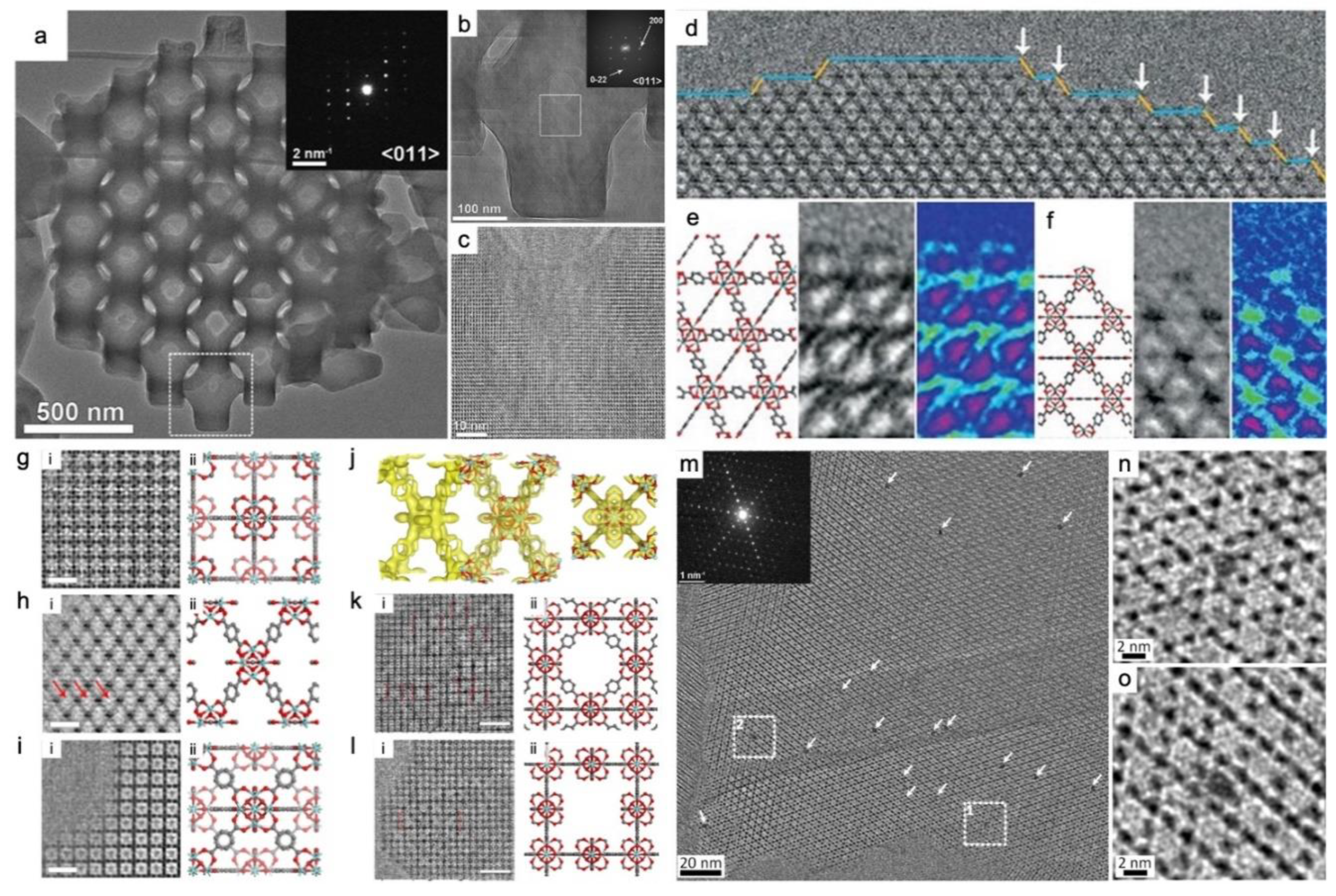
Figure 3.
HRTEM imaging of ZIF-8(Zn)[75], UiO-66(Zr)[14,25] and Mn12Ac@NU-1000(Zr)[81] using DDEC cameras. (a-c) Bulk of ZIF-8(Zn) with single-crystalline nature at different magnifications taken along the [011] zone axis. The inset of (a) shows the corresponding ED patterns, and the inset of (b) shows the indexed FT patterns. (b) and (c) are magnified views of the white square areas in (a) and (b), respectively[75]. (d-f) A truncation surface in a thermally treated UiO-66(Zr), showing crystal growth steps involving small {100} (labeled in blue) facets and {111} facets (labeled in yellow). (d) The white arrows point “kink” positions between {100} and {111} facets. (e) Ligand-terminated {111} surface: (left) structural model, (middle) HRTEM image by real-space averaging; (right) the averaged image in rainbow colors to increase the visibility of the ligand contrast. (f) Metal-terminated (ligand-free) {100}/{111} kink: (left) structural model; (middle) HRTEM image by real-space averaging; (right) the averaged image in rainbow colors[25]. (g-i) Missing linker defects and missing cluster defects in UiO-66(Zr). (g-j) Missing linker defects. CTF-corrected HRTEM images in column (i) and the projected structural model (Zr, cyan; O, red; C, grey; H atoms) in column (ii) along the [001] (g), [100] (h) and [110] (i) zone axes. Scale bars, 2 nm. (j) The reconstructed 3D electrostatic potential map viewed in two different orientations, showing an 8-connected network with the Zr6O8 clusters, BDC linkers and defect-terminating ligands (formates), with H atoms omitted for clarity. (k, l) Missing cluster defects viewed from the [001] direction, adopting the reo (k) and the scu structure (l). Column (i) show CTF-corrected HRTEM images and column (ii) shows the projected structural model (Zr, cyan; O, red; C, grey; H atoms). Scale bars, 5 nm[14]. (m-o) Guest species and host MOF: Mn12Ac@NU-1000(Zr). (m) HRTEM image and ED pattern (inset) of Mn12Ac@NU-1000 acquired along the [001] zone axis of NU-1000. Arrows point to the Mn12Ac clusters. (n, o) Enlarged images of the highlighted areas in areas 1 and 2 in (m), respectively. Mn12Ac clusters are shown to be encapsulated and fitted in the hexagonal channels of NU-1000(Zr)[81].
For minimization of the electron beam irradiation, fast seeking of the zone axis is essential for the DDEC camera. The time-consuming process of switching back and forth between imaging and diffraction modes in the traditional manual method results in the passive and undesirable acceptance of hundreds of electrons per Å2. A program [25] was developed to achieve a direct and one-step alignment of the zone axis for crystals whose initial orientations are close to the zone axis within 5° with a total dose well below 1 e- Å-2. This was conducted by calculating tilt angles from Laue circles identified from off-axis ED patterns. Additionally, when using a DDEC camera, the technique of dividing the exposure into stacks of sequential short-exposure frames to reduce the effects of electron beam-induced specimen motion requires the precise elimination of drift between frames. To address this, an "amplitude filter" was developed to limit the phase analysis to "reliable" high amplitude pixels [25]. This program contributed to the detection of organic linkers with lower atomic numbers on the surface of UiO-66(Zr).
In addition, the thickness effect is important for the phase contrast image captured by the DDEC camera, especially for the inorganic samples that are sensitive to irradiation. It is often necessary to have a simulation or image that directly corresponds to the position of the atoms and the contrast for an accurate interpretation.
Novel DDEC cameras, which allow direct imaging of MOFs at very low electron doses due to their high quantum detection efficiency, are a huge boost for HRTEM, enabling nondestructive visualization for MOFs materials under well-controlled conditions (Table 1). Nevertheless, HRTEM images taken with DDEC cameras still require a series of defocused images as those taken with scintillator-based cameras for a reasonable image correction and interpretation. The low-electron dose basic principle required by MOFs presents a challenge in determining Scherzer defocus, an issue that the DDEC cameras are not yet able to overcome.
3.3. Traditional STEM and iDPC-STEM
In terms of interpretation for high-resolution images, the coherent electron beam for TEM mode results in contrast reversion with defocus. It is necessary to determine the true structural information through a series of defocused images and subsequent analysis based on crystallographic principles. With a convergent electron beam, STEM mode has a higher resolution due to incoherent phase scattering imaging. Bragg diffraction exists only in the low angle bright-field (BF) and annual dark-field (ADF) imaging modes. The contrast of ADF images is proportional to the one-third power of the atomic number. The high-angle annual dark-field (HAADF) mode produces Z-contrast images, in which the contrast is proportional to the square of the atomic number. Due to the small scattering angle, elements with low atomic numbers are challenging to image. Nevertheless, STEM images are convincing to directly identify elements with a relatively obvious difference in contrast between them in the sample.
Therefore, the STEM mode has obvious advantages over the traditional TEM mode for its ability to accurately image non-periodic local structures such as defects, boundary surfaces, and deformations in crystals [18,74,82,83] and to analyze chemical elements.[26] Cs correctors also enhance the spatial resolution of the STEM mode [71].
The pore structures and super-tetrahedron building blocks of MIL-101(Cr) were observed using ADF-STEM with the beam current of <10 pA and the convergence semiangle of 22 mrad, which validated the controlled synthesis of a well-defined morphology (Figure 4a–c) [84]. With the probe size of 0.8 Å, and the beam current of <1.65×10⁻¹⁰A using a convergence semiangle of 17 mrad, the HAADF images permitted for the first time "quasi" atomic resolution imaging for nanometer MOF-74(Zn) prepared at room temperature (Figure 4d,e) [38]. The Zn clusters arranged in a hexagonal distribution were identified according to the bright features of the strong scattering factor in the HAADF image. The high crystallinity of MOF-74(Zn) was confirmed by the FFT-shown 6-fold axis indexed by a = b =25.93 Å, c=6.83Å, α=β=90°, and γ=120°. The probe size was set to 2.5 Å, and the spatial resolution was 0.8 Å (Figure 4f,g) [85]. Cs-corrected HAADF-STEM images were able to visualize layer stackings and identify “missing clusters” defects, which are missing one and a row of clusters, respectively, in 2D Hf-MOFs [46]. Regarding the imaging of host-guest interactions, ADF-STEM mode with the beam current set to ≤10 pA revealed that the ALD approach was suitable for the uniform deposition of Pt nanoparticles into the pores of MIL-101(Cr) and there was no structural degradation during the loading process (Figure 5a,b) [84]. In addition to metal guests, HAADF-STEM with the beam current down to 2 pA was conducted to observe the distributions of CsPbI3 perovskite QDs in order to validate the two-step synthetic method at room temperature for encapsulating the QDs in the pores of MIL-101(Cr). Anomalous contrast revealed QDs that were homogeneously distributed throughout the MOF crystal but did not occupy all the nanocages, demonstrating that MOF crystal can act as a stable reactor for QDs (Figure 5c,d) [86]. HAADF-STEM also investigated the anchoring of the W(≡CtBu)(CH2tBu)3 complex on mesoporous NU-1000(Zr) with high crystallinity using the surface organometallic chemistry (SOMC) method, with a convergence semiangle of 14.9 mrad [87].
Thus, it’s a key issue to reduce the hybrid materials’ structural collapse such as external defects or lattice damage caused by the STEM high-energy electron beam. Common use of multiple detectors is favored when necessary for practical considerations, such as the optical properties of the elements[85]. In STEM mode, the small electron beam is tracked on the small target area of the sample while the rest of the crystal is intact. It is a potential method to increase the electronic sensitivity of the detector. Besides, the spatial resolution of imaging is remarkably improved by the spherical aberration corrector. However, especially in Cs-STEM, beam-sensitive materials’ structure is easily burned out and even holes can be formed by the highly focused electron points. The electron dose and exposure time should be strictly controlled. The traditional method to reduce the electron dose in STEM mode mainly includes: diminishing the number of emitted electrons by stepping down the emission voltage of the electron gun and accelerating the scanning speed to decrease their dwell time on the pixel. The former probably worsens the accuracy of aberration correction, and the latter destabilizes the scanning coil.
To further address this issue, the concept of compressive sensing was introduced [74], where an image is represented by a sparse base set containing binary random missing pixels and can be recovered at a low sampling frequency. Using line-hopping approximate random adaptive sub-sampling, specimens can be imaged with high resolution and sensitivity, extremely low dose conditions (≤1 e- Å-2), as well as rather fast imaging, the effect of which is equivalent to the electron dose multiplied by at least one order of magnitude. Atomic-level resolution data on crystal structure can be obtained under combined control of the electron dose and the number of electrons per pixel (the beam current), manifesting its potential for in-situ observation [38].
To achieve a lower dose, higher signal-to-noise ratio, and better contrast, an emerging iDPC-STEM technique provides high efficiency in electron signal collection. It is equipped with four-quadrant segmented detectors, which can be utilized in the new generation of Cs-STEM without the need to install additional commercially available equipment (Figure 6) [18]. The electrostatic potential information of the lattice projection is reflected by the direct electronic phase imaging mode, of which image contrast is approximately linear with the atomic number. Light and heavy elements can be differentiated at sub-Å resolution simultaneously[18,30]. With sufficient electron utilization and a filter of vector field information such as non-integrable noise during the image integration process, iDPC-STEM features a high resolution and signal-to-noise ratio under the condition of extremely low electron dose. These advantages are comparable to (A)BF and (HA)ADF under the same low-dose conditions, with damage-freeness as a prerequisite. In a practical experimental comparison of HAADF and iDPC images, cages of MIL-101(Cr) were identified with the same resolution of 4.7 Å, using a beam current of 2 pA and a total dose of 54 e- Å-2 [88]. HAADF had its limitations for the challenge of imaging light atoms (Figure 5g–n), despite the fact that HAADF is little affected by the deflection of the crystal zone axis[89], but can serve as a reference to outline the structures [53]. iDPC-STEM entitles low-dose imaging of high-crystallinity materials sensitive to beams such as MOFs to great potential [30,90]. The imaging capability of low-dose iDPC-STEM for local structures is comparable to that of DDEC cameras at cryogenic temperatures [18]. Compared to HRTEM, iDPC-STEM makes the images highly interpretable due to the direct correlation between the contrast and the atomic number of the elements.
Utilizing the iDPC-STEM technique, the surface cage structure of MIL-101(Cr) was imaged with 1 pA probe current exposing for 12.6 s, the convergent half-angle set to 14.9 mrad, and the collection angle 16-61 mrad. The total electron dose of each image was as low as ~35 e- Å-2. The resolution was slightly lower than the 2.5 Å of HRTEM, but the contrast is stronger (Figure 7a–c). The MIL-101(Cr) samples were prepared by three methods, two with respective additives, hydrofluoric acid, and acetic acid, and one without additives. The significant function of acidic additives in influencing the crystal surface structure of MOFs was demonstrated by signifying the uniformity of {111} surfaces and the integrity of the surface cages of the three MIL-101(Cr) [40]. Also for MIL-101(Cr), the {111} surface of the two crystals was resolved at 1.8 Å, through the reduction of the electron beam current less than 0.1 pA (corresponding to the electron flux of 40 e- Å-2) and the setting of the convergence half-angle to 10 mrad. It was found that neither organic ligands nor lattice mismatches were present on the attached and connected {111} surfaces during the surface-to-surface assembly process of two MIL-101(Cr) crystals. Complete feature cages with sizes of 29 Å and 34 Å coexisted, and nearly half of them terminated two completely different types of surface terminations. The dual crystal interface structure preferred the 34 Å cage as the energy-stable termination point, and the adjacent edges maintained the 29 Å cage on the surface. Then a matching interface formed after the original lattice was rotated horizontally and moved about 18 Å (Figure 7d–i) [18]. iDPC-STEM also helped to elucidate the local structure evolution of MIL-101(Cr) under beam irradiation [88].
As for a newly-developed “molecular compartment” strategy to grow TiO2 inside different pores of MIL-101(Cr) and its derivatives, the precise characterization of TiO2 locations in real space poses great influence on understanding of synergetic mechanisms to improve photocatalytic CO2 reduction. Pure MOF and TiO2-in-MOF composites were characterized with interpretable resolutions of 3.9 Å and 5.2 Å for HAADF images and increased to 3.2 Å and 3.1 Å for iDPC-STEM images. iDPC-STEM images for light element contrast were more friendly and help to determine the exact location of mesopores in the MOF and the filling of TiO2 units relative to the MOF lattice (Figure 5g–n) [53]. Introduction of lattice strain, unsaturated metal sites, and defects were revealed by iDPC-STEM with the beam current <1 pA as the mechanism by which the incorporation of Fe3+ and 2-aminoterephthalate (ATA) increased the OER activity of Ni-BDC. “Missing linker” defects were observed in the thermal-treated multivariate MOFs and were thought to be caused by the removal of ATA. This MOF was denoted as FeNi-BA-T (Figure 7j–l) [91]. It is worth mentioning that iDPC-STEM technique has enabled simultaneous imaging of the MOFs and encapsulated single metal atoms [92]. iDPC-STEM technique made it possible to image the host UiO-66(Zr) and the guest Pt or Pd single atoms in the meantime with a beam current <0.1 pA. Atomic-scale details revealed the adsorption sites of the single atoms: the single Pt atom was located on the benzene ring of the BDC ligand in Pt@UiO-66, while the single Pd atom was absorbed by the BDC ligands. The amino group did not always facilitate the formation of single-atom catalysts, as the metals in Pt@UiO-66-NH2 and Pd@UiO-66 presented as clusters (Figure 5e,f) [92].
Spectroscopic analysis based on high-resolution imaging is a powerful tool for probing the chemical composition of samples at the microscopic scale. STEM-EDS (EDS: energy dispersive spectroscopy) and STEM-EELS (EELS: electron energy loss spectroscopy) have been effectively applied to MOFs materials such as UiO-66(Zr) [93]. Nevertheless, the conventional elemental information acquisition procedure takes a long time, which aggravates the degree of MOFs degradation. Under cryogenic conditions, damage-free and monochromated STEM-EELS was performed on MIL-100(Al), MIL-100(Fe), and UiO-66(Zr) at an energy resolution of 7 meV, a low electron flux of 10 e- Å-2 and a convergence semiangle of 10 mrad, using a DDEC camera. By monitoring the evolutions of characteristic peaks with the controlled electron dose (from 10 e- Å-2 to 104 e- Å-2), coordination bonds were studied, and chemical group distributions with their intact and degraded parts were discovered for the three MOFs in the energy range, then mapped with a spatial resolution of 10 nm. This research offered a methodological reference for the chemical property analysis of beam-sensitive materials in the wide energy range, including infrared (IR), ultraviolet (UV), and X-ray intervals [94].
Figure 5.
Traditional and iDPC-STEM characterization of host MOFs and guest species encapsulated: Pt@MIL-101(Cr)[84], CsPbI3@MIL-101(Cr)[86], Pt@UiO-66(Zr)[92], TiO2-in-MIL-101(Cr) composites[53]. (a, b) ADF-STEM images and corresponding FFT along [011] zone axis of an MIL-101(Cr) crystal loaded with Pt nanoparticles, showing that the size of Pt nanoparticles are tailored to that of MIL-101 pores. The white and red arrows point to nanoparticles at small and large cage positions, respectively (in projection)[84]. (c, d) HAADF-STEM images of MIL-101(Cr) crystal whose cavities filled by the perovskite material CsPbI3 along the [110] direction. (c) The occupied CsPbI3 nanoparticles in the pores are seen as 1.14 nm bright circles, which are separated by 5−6 nm. (d) The loaded image with the MIL-101(Cr) schematic model superimposed along the [110] orientation. Red, blue, and yellow circles indicate 2.9 nm cage, 3.4nm cage, and supertetrahedra, respectively[86]. (e, f) iDPC-STEM images of UiO-66(Zr) crystal encapsulated Pt (e) and Pt (f) single atoms[92]. (g-n) iDPC-STEM images TiO2-in-MIL-101(Cr) composites. (g-l) Raw and filtered HAADF images (g-i) and iDPC-STEM (j-l) images taken from the [110] projection: MIL-101-Cr (g, j), 23%-TiO2-in-MIL-101-Cr (h, k) and 42%-TiO2-in-MIL-101-Cr (i, l). Red and blue outlines highlight the positions of TiO2 units in separate types of mesopores, with the unit cell shown in orange. Scale bars, (g-l), 5 nm. (m) 2D projected potential map (greyscale; middle) obtained by imposing c2mm plane group symmetry, generated from iDPC-STEM images, and overlaid with pore arrangement (top) and atomic structure (bottom). (n) Atomic structure and topology of compartment I (based on mesopore I of 29 Å, outlined in blue) and compartment II (based on mesopore II of 34 Å, outlined in red)[53].
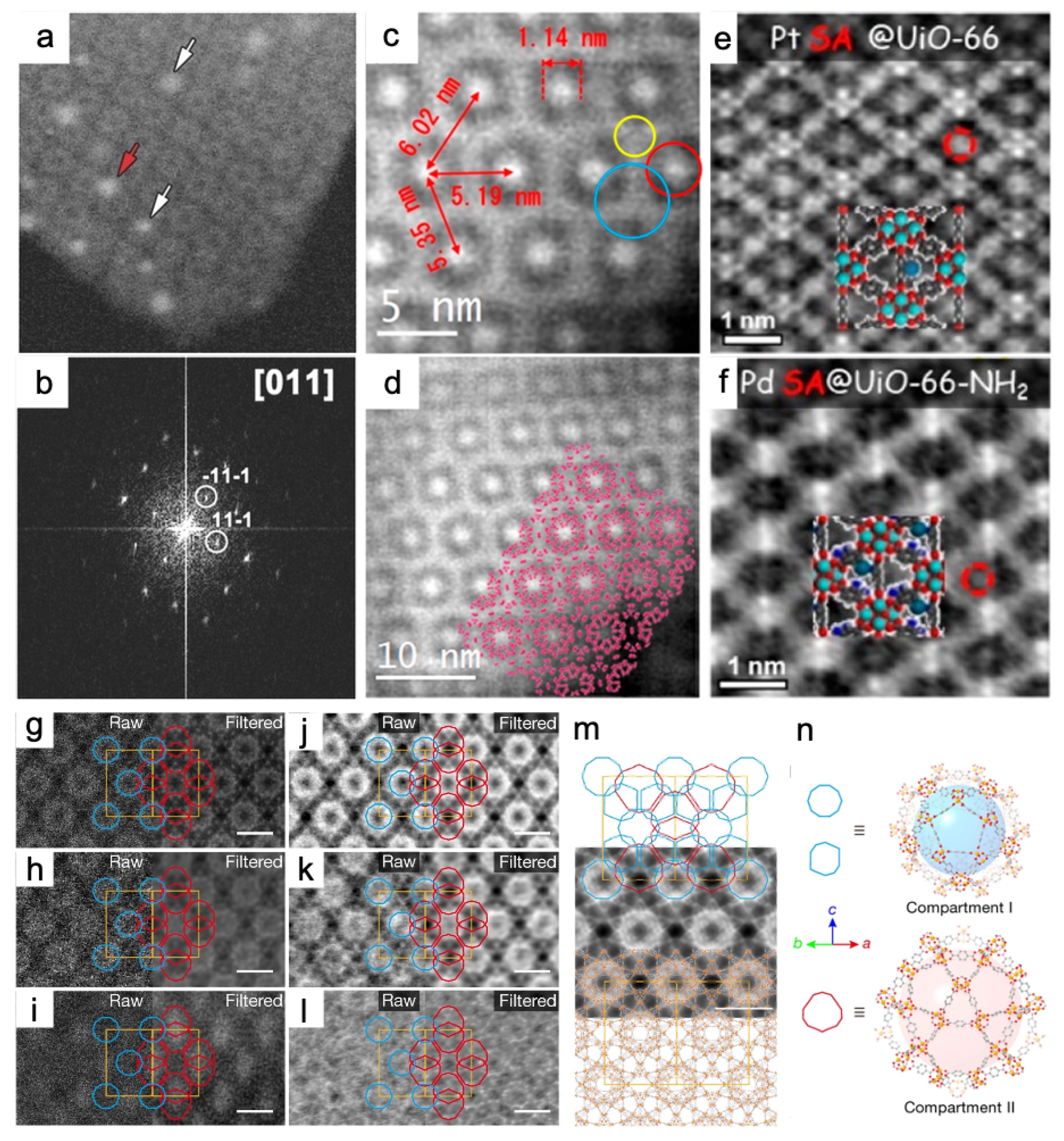
Figure 6.
iDPC-STEM schematic set-up and exemplary images of MIL-101(Cr) along [110] projection[18]. (a)The schematic set-up of iDPC-STEM. The electron beam is deflected by the potential field in specimens and detected by the four segments of DPC detector. (b) Four images detected by the four segments (A-D) of DPC detector, respectively. Scale bar, 20 nm. (c) The DPC image obtained from the four images in (b). Scale bar, 20 nm. (d) The iDPC-STEM image obtained by a 2D integration of the DPC image in (c). Scale bar, 10 nm. (e) The magnified iDPC-STEM image perfectly matched the structural model. Scale bar, 5 nm. (f) The corresponding FFT pattern of (e) in a log scale with an information transfer up to 1.8 Å.
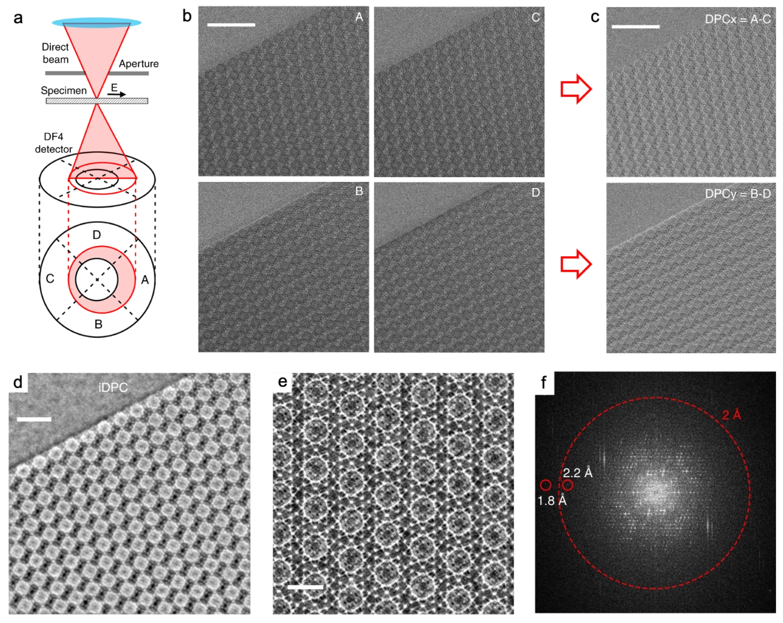
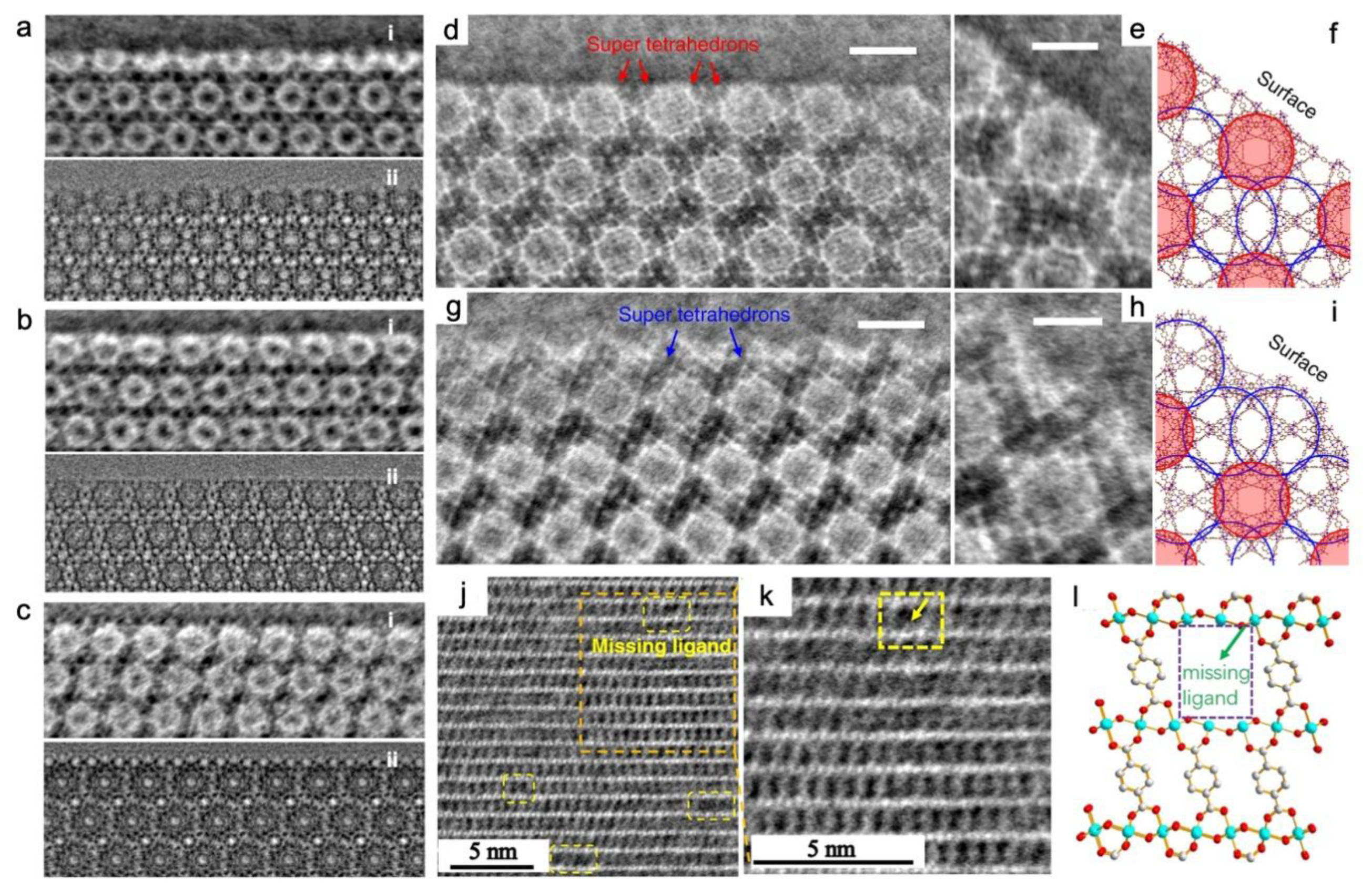
Figure 7.
iDPC-STEM imaging of MIL-101(Cr)[18,40] and FeNi-BA-T[91]. (a-c) iDPC-STEM images (row (i) in (a-c)), and CTF-corrected HRTEM images (row (ii) in (a-c)) of the same sample, which show MIL-101(Cr) surface structures. Three vacuum-heated samples using different additives: (a) MIL-101-HF (HF), (b) MIL-101-Ac (acetic acid), and (c) MIL-101-NA (no additive). Scale bars, 5 nm[40]. (d-i) Surface characterizations of MIL-101(Cr). iDPC-STEM images of two types of surface terminations with two types of cages exposed on the {111} surfaces in a MIL-101 crystal: one in (d) exhibits the complete characteristic spheres along the {111} surfaces, whereas another in (g) is terminated by nearly half of the spheres. The structures of single-unit cells at two types of surface terminations are shown in (e) and (h), respectively, of which the structural models are in (f) and (i). Scale bars, (d, g), 5 nm, (e, h), 3 nm[18]. (j-l) Missing linker defects in FeNi-BA-T. (j) iDPC-STEM images of FeNi-BA-T. (k) The enlarged image of the blanket in (j) showing the missing ligand defect. (l) The projected structural model of FeNi-BA-T[91].
3.4. Dynamic visualization by in-situ TEM
3.4.1. In-situ synthesis
Liquid phase is one of the important synthetic conditions for MOFs, where chemical interactions usually produce many tiny intermediates that quickly reach equilibrium[95]. In-situ LCTEM provides insights into MOF synthesis in solution by directly visualizing their nucleation, growth. and self-assembly dynamics. Experimental synthetic conditions such as concentration, temperature, node/linker ratio can be realized by in-situ LCTEM and subsequently verified by ex-situ TEM. It is feasible to investigate the liquid-phase synthesis conditions and in-depth mechanisms through the contrast, morphology, and growth behavior of MOFs. Given the MOFs’ beam-sensitivity, emphasis should be placed on the electron tolerance and methods to reduce damages to the particles to be synthesized in liquid, as well as control of the surface chemistry of the LC viewing membrane along with the electron beam conditions.
As for macromolecular self-assembled materials, LCTEM was performed almost at the beginning to visualize the dynamics of ZIF-8(Zn), which allows low-temperature formation with a cumulative dose of ~20 times less than the damage threshold of ~4000 e- nm-2. Nucleation was limited by the local consumption of the monomer in the solution and controlled reproducibly by physical stirring instead of an electron beam when monomers were continuously fed into the LC. The growth was a surface reaction limited process in which the growth rate and particle size were controlled by the ratio of metal to ligand rather than particle coalescence [42]. Later, the nucleation of ZIF-8(Zn) was recorded and considered to follow a three-step nonclassical nucleation pathway. Images were recorded by the DDEC camera at a rate of 20 frames per second with the electron dose rate controlled to ≤0.05 e- Å-2 s-1, and manipulated by averaging every five consecutive raw frames to enhance the signal-to-noise ratio. Phase separation by mass of solute concentration, condensation of a solute-rich region into an amorphous aggregate, and aggregate crystallization were the three steps (Figure 8a,b) [45].
Metal-organic layers (MOL, referred to as 2D MOFs) have attracted attention due to the merits of 2D materials and MOFs. The multi-step nucleation process of Hf-MOL revealed that Hf-clusters were first formed in solution, then were complexed with ligands to form amorphous precursors, followed by the cluster-ligand complexes into hexagonally arranged nuclei. The addition of clusters to the surface edges may have served as the pathway to subsequent growth. High-quality imaging of organic ligands was important to determine this formation pathway (Figure 8c,d) [46].
It is fascinating to explore the properties and applications of metal-organic nanotubes (MONTS, referred to 1D MOFs), which also feature tunable interconnected networks. LCTEM provides opportunities to elucidate the formation mechanisms of discrete or small bundles of tubes. With respect to [(L1)Cu2Br2](L1=1,4-bis((4H-1,2,4-triazol-4-yl)methyl)naphthalene), initial nucleation events failed to be captured due to limited imaging contrast and resolution at the electron dose of <10 e- Å-2. The heating function provided by the chip of LCTEM found that [(L1)Cu2Br2] grew more than 3 times faster at 85°C than at 23°C. The thermodynamically driven process was depicted as a surface-specific monomer-monomer attachment, where precursor ions or amorphous clusters continuously underwent anisotropic growth to form MONT crystals after determining the lowest energy surface for crystal growth [72]. This research group then investigated the growth of Ag-MONTs that were also based on L1 ligands. Unlike the previously investigated systems [72], such MONTs crystals formed via multiple pathways depending on the reaction conditions. In a comparatively short amount of time, the precursor ions aggregated and formed short-range clusters to minimize energy, resulting in primary particles that were non-homogeneously nucleated and developed into anisotropic MONTs bundles as supersaturation advanced [96].
However, it is still difficult to perform ED on MOFs in a liquid environment, because of the background signal and electron scattering from the liquid layer and the fluctuation of small specimens. ED can be performed by post-mortem after drying the liquid or by plunge-freezing the reaction solutions at the moment of interest and then using cryo-TEM [45].
3.4.2. Phase transition
MOFs’ topological structures diversify due to the coordination between organic linkers and metal clusters. For example, the Zr6--MOFs are composed of [Zr6(μ-O)4(μ-OH)4]12+ clusters and multi-host carboxylate-based organic linkers, with 10 topological structures and pore structures [97]. The design of pure-phase MOFs requires an understanding of the conditions and mechanisms governing the transitions between multiple phases.
The phase transition of Zr6--MOFs from microporous scu-NU-906 with a characteristic lattice spacing of ~1.7 nm to mesoporous csq-NU-1008 of ~3.5 nm was directly observed at 80°C using LCTEM with a flow cell, and the cumulative electron dose was limited to <6 e- Å-2 [97]. The process followed the dissolution-reprecipitation mechanism and was tunable by the formic acid concentration and reaction time. Its principle was demonstrated: formic acid promoted the dissolution of NU-906 and acted as a regulator for the formation of the second phase NU-1008; the dissolution of NU-906 produced an intermediate solution containing Zr6 clusters, TCPB-Br2 linkers, excess formic acid, and DMF whose composition was the same as the initial synthesis solution of NU-1008, so the dissolution of NU-906 would simultaneously produce NU-1008.
3.4.3. Pore breathing
The periodic frameworks of MOFs are flexible with a large specific surface area. The host structure changes with changes in temperature and pressure or through reversible adsorption and desorption with the guest. The periodic frameworks of MOFs tend to experience reversible lattice transformations, a process known as pore "breathing", when external factors such as temperature and pressure fluctuate or when guests are adsorbed and desorbed. It is entitled to be gas storage and separation platforms for H2O vapor, N2, O2, CO2, CH4, H2, CO, NH3, etc. [98,99]. Using the low-dose setting of ~5 e- Å-2 cumulative dose, in-situ ETEM directly visualized the lattice changes of MIL-53(Cr) induced by the adsorption and desorption of H2O molecules on them during temperature cycles from heating to 300 °C to cooling to 27 °C. This pore breathing was originally triggered by the first adsorption of a single H2O molecule per unit cell of MIL-53(Cr) at 300 °C, according to molecular dynamics (MD) simulations. These first adsorbed H2O molecules were anchored by hydrogen bonds formed between them and the bridging μ-OH groups of MIL-53(Cr) during this activation process and remained stable throughout the following temperature-modulated adsorption and desorption[100].
3.4.4. On demand structural modification
Damage-free characterization requires the determination of the threshold of the cumulative electron dose at which MOFs start to collapse. However, structural modification may occur earlier beyond the detection limit. A guideline for maximizing the integrity of MOFs can be found in the quantitative characterization of the local structural evolution under in situ irradiation and the underlying mechanisms.
Observed at a resolution of 4.7Å using iDPC-STEM technique, the local evolution of the pores of MIL-101(Cr) single crystals was found to depend on both the crystal plane and the specific position in the crystal (Figure 9a–f). At the molecular level, importance was attached to super tetrahedrons, which were composed of μ3O-bridged trimetric chromium oxide clusters and organic linkers. Through quantitative analysis of irradiation, the shrinkage and deformation of crystals with the increase in electron dose might be attributed to the molecular displacement and asymmetric component distribution that were inhomogeneous within the single MOF crystal [88]. The structural evolution of ZIF-L(Zn) was captured using a DDEC camera with a dose rate of 0.25 e Å-2 s-1 (20 frames with 0.5 s/frame exposure). Notably, the electron beam-induced degradation of ZIF-L(Zn) was divided into two stages according to the accumulated electron flux threshold of 100 e Å-2 s-1. The first stage was the widely reported structural damage, which was manifested by significant deformation and amorphization in the TEM observation region. The second stage was the molecular breakdown of the organic linker 2-methyl-imidazole (2-mIm). It severely affected the dielectric function and energies of electronic transitions as determined by core-loss EELS C and N K-edge analysis [101].
Due to the uniform internal pore structures, long-range ordered MOFs crystals are suitable as templates for the formation of monodisperse particles and clusters, and other nanomaterials. To this end, TEM was used to rapidly induce MOFs degradation to form Ag nanoclusters with a size of only a few to tens of atoms [102] and Cu nanoparticles with a tunable size from a few nanometers to a few hundred nanometers [103]. In-situ heating sample holder enabled and visualized the formation of Ni nanoparticles from carbonization of Ni-MOFs. The transformation process began significantly at 400 °C, and Ni nanoparticles tended to aggregate and be wrapped in the carbon matrix after reaching 700 °C. This was concerned with the increased crystallinity of the Ni nanoparticles and the stability of the carbon matrix at high temperatures [104]. Structural transformation of ZIF-67(Co) during pyrolysis was monitored, whose derivative serves as ideal ORR catalyst templates. ZIF-67(Co) crystals underwent an ordered-disordered transition at 442 °C, precipitating Co atomic clusters and losing nitrogen, possibly due to the pyrolysis of CoN4 tetrahedra above 500 °C, after which considerable carbonization occurs above 800 °C [105]. Other research groups discovered that Co nanocrystals were uniformly dispersed in the early stages of carbonization, but as the temperature increased, they became larger and moved toward the carbon surface. Some of the tiny Co nanocrystals that escaped after heating to 1000 °C volatilized, while others catalyzed the formation of carbon nanotubes. During the pyrolysis, the carbon texture started to crystallize at 600 °C and is completely transformed at 800 °C [106]. Hollow layered double hydroxide (LDH) materials are promising in catalysis and energy storage. ZnCo(OH)x, a kind of LDH, was demonstrated by LCTEM to be formed based on continuous etching and similar growth rate of ZIF-8(Zn) and ZIF-67(Co)@ZIF-8(Zn) (Figure 9g,h). To effectively capture the dynamics, the electron dose rate was set to <0.1 e Å-2 s-1, and nanocubic and nanorhombic dodecahedrons were chosen, whose well-defined shapes made it easy to identify the reaction front [106].
4. Conclusion and outlook
MOFs, promising and unique in various applications, are susceptible to electron beam irradiation using powerful but challenging TEM methods. Key experimental considerations for the structural integrity of MOFs under electron irradiation include low electron dose and temperature. Traditional TEM-related methods have limited the research possibilities of MOFs, while groundbreaking discoveries have been made thanks to the advancement of new technologies and equipment in TEM including 3DED, DDEC camera, and iDPC-STEM. Static structural analysis at ultra-high spatial and temporal resolution makes it possible to unravel details of surfaces, interfaces, defectss, and host-guest interactions. Dynamic exploration provides insights into the mechanisms of MOF formation, phase transitions, pore breathing, and on-demand structural modification under electron beam irradiation.
Research advances in imaging MOFs using TEM are listed in Table 1, which includes key techniques, experimental conditions, and characterized structures. Regarding two fundamental concepts: (1) low-dose TEM: It is a guideline to be followed, and is one of the main features of both the advanced DDEC cameras used in TEM imaging mode and the new imaging method iDPC-STEM in STEM mode. The goal is to direct image beam-sensitive MOFs materials with high resolution and a high signal-to-noise ratio at an ultra-low electron beam dose. (2) cryo-TEM: In addition to fitting the characterization of biomacromolecule-MOFs, cryo-TEM reduces the irradiation damage of the sample during observation and can be used for post-mortem analysis of regions that are difficult to observe at the atomic scale in in-situ TEM. Regarding the range of applications of the techniques of the three categories. (1) ED: It is mainly used to characterize periodic structures. Investigations for non-periodic structures are less common, although local structures have been characterized by the 4D-STEM-based SED technique, and missing cluster defects have been identified and guest species in the frameworks have been localized using 3DED technique. It is worth mentioning that in addition to direct imaging, a method for in-situ TEM was realized in combination with ETEM and 3DED. (2) Imaging in TEM mode: DDEC cameras effectively maximize electron utilization during imaging. The structural interpretation is facilitated by CTF corrections, etc. (3) Imaging in STEM mode: It helps to identify the relative atomic numbers of elements directly from the image contrast. The advanced iDPC-STEM technique can simultaneously image light and heavy elements while improving electron utilization. Traditional STEM imaging techniques, including (HA)ADF, are complementary to structural analysis.
Further in-depth research on MOFs is expected to benefit from the continued development of current techniques, such as the cameras’ performance to acquire and use electron signals, and the imaging capability of low-voltage TEM. Furthermore, it is envisaged that increasingly evolving and innovative TEM-related techniques will be adaptable to MOFs, possibly even providing previously unobservable details. For instance, without sacrificing MOFs specimens, electron tomography [107] may help reconstruct the atomic-scale structure of MOFs alone or in combination with their guest species. And the data obtained from the reconstruction of the large-scale data acquired by 4D-STEM [108] provides information on stress and strain, as well as electric and magnetic field distributions, etc., in addition to the structures. Additionally, TEM imaging often requires samples with thicknesses <100 nm if possible, to reduce multiple scattering of electrons in the sample to satisfy the weak phase object approximation (WPOA) as closely as possible, although typically only the pseudo-weak phase object approximation (PWPOA) is satisfied. Sample thickness is also a challenge for low-dose imaging with high spatial resolution. However, the intrinsic size of the MOFs that need to be studied might not fulfill this criterion, but this can be improved by using sample-protective preparation methods and cutting-edge imaging techniques. For the former, cryo-focused ion beam (cryo-FIB) [109,110] is expected to be used to prepare MOFs crystals with sizes beyond the nanoscale into samples that are adaptable to TEM observation. This is due to the micro- and nano-processing capability of the ion beam and the protection to MOFs samples from ion beam damage during processing under cryogenic conditions. However, such studies are still scarce, because the existing technology is still difficult to meet the desired expectations, and there are great prospects for development. Such research is still in its infancy due to the difficulty of the currently practical methods in meeting the necessary expectations, but it shows great potential for technological advancement. Among the latter, multislice electron ptychography is promising for MOFs. This technique combines STEM and 2D coherent ED patterns and has been successfully used for the measurement of zeolite atomic structures, a type of material that is also sensitive to the electron beam [111]. An incorporated adaptive propagator helps to address the impact of specimen misorientations on the accuracy and reliability of the image [89].
It is envisioned that the novel and emerging TEM techniques will continue to provide critical understanding and be essential characterization approaches for MOFs as complementary to other characterization techniques.
Author Contributions
Conceptualization, A.Z. and K.Y.; Investigation, A.Z., R.P., M.Z. and Y.X; Researches, A.Z., R.P., M.Z. and Y.X; Writing - Original Draft Preparation, A.Z.; Writing - Review & Editing, A.Z. and K.Y.; Supervision, K.Y.; Project Administration, K.Y. and L.S.; Funding Acquisition, K.Y. and L.S. All authors have read and agreed to the published version of the manuscript.
Funding
This work was supported by the National Key R&D Program of China (No. 2020YFB2007402), the National Natural Science Foundation of China (No. 12174050, and 12234005), the Major Project of Natural Science Foundation of Jiangsu Province (BK20222007), the key Key R&D Program of Jiangsu Province (BE2021007-2), and the Fundamental Research Funds for the Central Universities.
Institutional Review Board Statement
Not applicable.
Informed Consent Statement
Not applicable.
Data Availability Statement
Not applicable.
Conflicts of Interest
The authors declare no competing financial interest.
References
- Furukawa, H.; Cordova, K.E.; O'Keeffe, M.; Yaghi, O.M. The Chemistry and Applications of Metal-Organic Frameworks. SCIENCE 2013, 341, 974. [Google Scholar] [CrossRef] [PubMed]
- Huang, Y.-B.; Liang, J.; Wang, X.-S.; Cao, R. Multifunctional metal-organic framework catalysts: synergistic catalysis and tandem reactions. CHEMICAL SOCIETY REVIEWS 2017, 46, 126–157. [Google Scholar] [CrossRef] [PubMed]
- Xue, D.-X.; Wang, Q.; Bai, J. Amide-functionalized metal-organic frameworks: Syntheses, structures and improved gas storage and separation properties. COORDINATION CHEMISTRY REVIEWS 2019, 378, 2–16. [Google Scholar] [CrossRef]
- Adil, K.; Belmabkhout, Y.; Pillai, R.S.; Cadiau, A.; Bhatt, P.M.; Assen, A.H.; Maurin, G.; Eddaoudi, M. Gas/vapour separation using ultra-microporous metal-organic frameworks: insights into the structure/separation relationship. CHEMICAL SOCIETY REVIEWS 2017, 46, 3402–3430. [Google Scholar] [CrossRef] [PubMed]
- Xia, W.; Mahmood, A.; Zou, R.; Xu, Q. Metal-organic frameworks and their derived nanostructures for electrochemical energy storage and conversion. Energy & Environmental Science 2015, 8, 1837–1866. [Google Scholar] [CrossRef]
- Hu, Z.; Deibert, B.J.; Li, J. Luminescent metal-organic frameworks for chemical sensing and explosive detection. CHEMICAL SOCIETY REVIEWS 2014, 43, 5815–5840. [Google Scholar] [CrossRef]
- Furukawa, H.; Gandara, F.; Zhang, Y.-B.; Jiang, J.; Queen, W.L.; Hudson, M.R.; Yaghi, O.M. Water Adsorption in Porous Metal-Organic Frameworks and Related Materials. JOURNAL OF THE AMERICAN CHEMICAL SOCIETY 2014, 136, 4369–4381. [Google Scholar] [CrossRef]
- Li, X.X.; Cheng, F.Y.; Zhang, S.N.; Chen, J. Shape-controlled synthesis and lithium-storage study of metal-organic frameworks Zn4O(1,3,5-benzenetribenzoate)(2). JOURNAL OF POWER SOURCES 2006, 160, 542–547. [Google Scholar] [CrossRef]
- McGuire, C.V.; Forgan, R.S. The surface chemistry of metal-organic frameworks. Chem Commun (Camb) 2015, 51, 5199–5217. [Google Scholar] [CrossRef]
- Han, X.; Liu, P.; Lin, F.; Chen, W.; Luo, R.; Han, Q.; Jiang, Z.; Wang, X.; Song, S.; Reddy, K.M.; et al. Structures and Structural Evolution of Sublayer Surfaces of Metal-Organic Frameworks. Angew Chem Int Ed Engl 2020, 59, 21419–21424. [Google Scholar] [CrossRef]
- Yanai, N.; Sindoro, M.; Yan, J.; Granick, S. Electric field-induced assembly of monodisperse polyhedral metal-organic framework crystals. J Am Chem Soc 2013, 135, 34–37. [Google Scholar] [CrossRef] [PubMed]
- Avci, C.; Liu, Y.; Pariente, J.A.; Blanco, A.; Lopez, C.; Imaz, I.; Maspoch, D. Template-Free, Surfactant-Mediated Orientation of Self-Assembled Supercrystals of Metal-Organic Framework Particles. Small 2019, 15, e1902520. [Google Scholar] [CrossRef] [PubMed]
- Bradshaw, D.; Garai, A.; Huo, J. Metal-organic framework growth at functional interfaces: thin films and composites for diverse applications. CHEMICAL SOCIETY REVIEWS 2012, 41, 2344–2381. [Google Scholar] [CrossRef] [PubMed]
- Liu, L.; Chen, Z.; Wang, J.; Zhang, D.; Zhu, Y.; Ling, S.; Huang, K.W.; Belmabkhout, Y.; Adil, K.; Zhang, Y.; et al. Imaging defects and their evolution in a metal-organic framework at sub-unit-cell resolution. Nat Chem 2019, 11, 622–628. [Google Scholar] [CrossRef] [PubMed]
- Johnstone, D.N.; Firth, F.C.N.; Grey, C.P.; Midgley, P.A.; Cliffe, M.J.; Collins, S.M. Direct Imaging of Correlated Defect Nanodomains in a Metal-Organic Framework. J Am Chem Soc 2020, 142, 13081–13089. [Google Scholar] [CrossRef]
- Shi, F.L.; Li, F.; Ma, Y.L.; Zheng, F.Y.; Feng, R.; Song, C.Y.; Tao, P.; Shang, W.; Deng, T.; Wu, J.B. In Situ Transmission Electron Microscopy Study of Nanocrystal Formation for Electrocatalysis. ChemNanoMat 2019. [Google Scholar] [CrossRef]
- Cliffe, M.J.; Wan, W.; Zou, X.; Chater, P.A.; Kleppe, A.K.; Tucker, M.G.; Wilhelm, H.; Funnell, N.P.; Coudert, F.X.; Goodwin, A.L. Correlated defect nanoregions in a metal-organic framework. Nature Communications 2014, 5, 4176. [Google Scholar] [CrossRef]
- Shen, B.; Chen, X.; Shen, K.; Xiong, H.; Wei, F. Imaging the node-linker coordination in the bulk and local structures of metal-organic frameworks. Nat Commun 2020, 11, 2692. [Google Scholar] [CrossRef]
- Zahmakiran, M. Iridium nanoparticles stabilized by metal organic frameworks (IrNPs@ZIF-8): synthesis, structural properties and catalytic performance. Dalton Trans 2012, 41, 12690–12696. [Google Scholar] [CrossRef]
- Esken, D.; Turner, S.; Lebedev, O.I.; Van Tendeloo, G.; Fischer, R.A. Au@ZIFs: Stabilization and Encapsulation of Cavity-Size Matching Gold Clusters inside Functionalized Zeolite Imidazolate Frameworks, ZIFs. CHEMISTRY OF MATERIALS 2010, 22, 6393–6401. [Google Scholar] [CrossRef]
- Li, Z.; Wang, G.; Ye, Y.; Li, B.; Li, H.; Chen, B. Loading Photochromic Molecules into a Luminescent Metal-Organic Framework for Information Anticounterfeiting. ANGEWANDTE CHEMIE-INTERNATIONAL EDITION 2019, 58, 18025–18031. [Google Scholar] [CrossRef] [PubMed]
- Lu, G.; Li, S.; Guo, Z.; Farha, O.K.; Hauser, B.G.; Qi, X.; Wang, Y.; Wang, X.; Han, S.; Liu, X.; et al. Imparting functionality to a metal-organic framework material by controlled nanoparticle encapsulation. Nat Chem 2012, 4, 310–316. [Google Scholar] [CrossRef] [PubMed]
- Cui, Y.; Li, B.; He, H.; Zhou, W.; Chen, B.; Qian, G. Metal-Organic Frameworks as Platforms for Functional Materials. ACCOUNTS OF CHEMICAL RESEARCH 2016, 49, 483–493. [Google Scholar] [CrossRef] [PubMed]
- Egerton, R.F. Mechanisms of radiation damage in beam-sensitive specimens, for TEM accelerating voltages between 10 and 300 kV. Microsc Res Tech 2012, 75, 1550–1556. [Google Scholar] [CrossRef] [PubMed]
- Zhang, D.; Zhu, Y.; Liu, L.; Ying, X.; Hsiung, C.E.; Sougrat, R.; Li, K.; Han, Y. Atomic-resolution transmission electron microscopy of electron beam-sensitive crystalline materials. SCIENCE 2018, 359, 675–679. [Google Scholar] [CrossRef]
- Turner, S.; Lebedev, O.I.; Schroder, F.; Esken, D.; Fischer, R.A.; Van Tendeloo, G. Direct imaging of loaded metal-organic framework materials (metal@MOF-5). CHEMISTRY OF MATERIALS 2008, 20, 5622–5627. [Google Scholar] [CrossRef]
- Wiktor, C.; Turner, S.; Zacher, D.; Fischer, R.A.; Van Tendeloo, G. Imaging of intact MOF-5 nanocrystals by advanced TEM at liquid nitrogen temperature. MICROPOROUS AND MESOPOROUS MATERIALS 2012, 162, 131–135. [Google Scholar] [CrossRef]
- Huang, Z.; Willhammar, T.; Zou, X. Three-dimensional electron diffraction for porous crystalline materials: structural determination and beyond. Chemical Science 2021, 12, 1206–1219. [Google Scholar] [CrossRef]
- Li, X.; Mooney, P.; Zheng, S.; Booth, C.R.; Braunfeld, M.B.; Gubbens, S.; Agard, D.A.; Cheng, Y. Electron counting and beam-induced motion correction enable near-atomic-resolution single-particle cryo-EM. NATURE METHODS 2013, 10, 584. [Google Scholar] [CrossRef]
- Lazic, I.; Bosch, E.G.T.; Lazar, S. Phase contrast STEM for thin samples: Integrated differential phase contrast. ULTRAMICROSCOPY 2016, 160, 265–280. [Google Scholar] [CrossRef]
- Huang, Z.; Grape, E.S.; Li, J.; Inge, A.K.; Zou, X. 3D electron diffraction as an important technique for structure elucidation of metal-organic frameworks and covalent organic frameworks. COORDINATION CHEMISTRY REVIEWS 2021, 427. [Google Scholar] [CrossRef]
- Yang, T.; Willhammar, T.; Xu, H.; Zou, X.; Huang, Z. Single-crystal structure determination of nanosized metal-organic frameworks by three-dimensional electron diffraction. Nature Protocols 2022, 17, 2389–2413. [Google Scholar] [CrossRef] [PubMed]
- Wiktor, C.; Meledina, M.; Turner, S.; Lebedev, O.I.; Fischer, R.A. Transmission electron microscopy on metal-organic frameworks - a review. Journal of Materials Chemistry A 2017, 5, 14969–14989. [Google Scholar] [CrossRef]
- Liu, L.; Zhang, D.; Zhu, Y.; Han, Y. Bulk and local structures of metal-organic frameworks unravelled by high-resolution electron microscopy. Communications Chemistry 2020, 3. [Google Scholar] [CrossRef] [PubMed]
- Gong, X.; Gnanasekaran, K.; Chen, Z.; Robison, L.; Wasson, M.C.; Bentz, K.C.; Cohen, S.M.; Farha, O.K.; Gianneschi, N.C. Insights into the Structure and Dynamics of Metal-Organic Frameworks via Transmission Electron Microscopy. JOURNAL OF THE AMERICAN CHEMICAL SOCIETY 2020, 142, 17224–17235. [Google Scholar] [CrossRef]
- Zhang, J.; Cheng, N.; Ge, B. Characterization of metal-organic frameworks by transmission electron microscopy. Advances in Physics-X 2022, 7. [Google Scholar] [CrossRef]
- Egerton, R.F.; Li, P.; Malac, M. Radiation damage in the TEM and SEM. MICRON 2004, 35, 399–409. [Google Scholar] [CrossRef]
- Diaz-Garcia, M.; Mayoral, A.; Diaz, I.; Sanchez-Sanchez, M. Nanoscaled M-MOF-74 Materials Prepared at Room Temperature. CRYSTAL GROWTH & DESIGN 2014, 14, 2479–2487. [Google Scholar] [CrossRef]
- Lebedev, O.I.; Millange, F.; Serre, C.; Van Tendeloo, G.; Ferey, G. First direct imaging of giant pores of the metal-organic framework MIL-101. CHEMISTRY OF MATERIALS 2005, 17, 6525–6527. [Google Scholar] [CrossRef]
- Li, X.; Wang, J.; Liu, X.; Liu, L.; Cha, D.; Zheng, X.; Yousef, A.A.; Song, K.; Zhu, Y.; Zhang, D.; et al. Direct Imaging of Tunable Crystal Surface Structures of MOF MIL-101 Using High-Resolution Electron Microscopy. J Am Chem Soc 2019, 141, 12021–12028. [Google Scholar] [CrossRef]
- Zhu, Y.; Ciston, J.; Zheng, B.; Miao, X.; Czarnik, C.; Pan, Y.; Sougrat, R.; Lai, Z.; Hsiung, C.E.; Yao, K.; et al. Unravelling surface and interfacial structures of a metal-organic framework by transmission electron microscopy. Nat Mater 2017, 16, 532–536. [Google Scholar] [CrossRef] [PubMed]
- Patterson, J.P.; Abellan, P.; Denny, M.S., Jr.; Park, C.; Browning, N.D.; Cohen, S.M.; Evans, J.E.; Gianneschi, N.C. Observing the growth of metal-organic frameworks by in situ liquid cell transmission electron microscopy. J Am Chem Soc 2015, 137, 7322–7328. [Google Scholar] [CrossRef] [PubMed]
- Feyand, M.; Mugnaioli, E.; Vermoortele, F.; Bueken, B.; Dieterich, J.M.; Reimer, T.; Kolb, U.; de Vos, D.; Stock, N. Automated diffraction tomography for the structure elucidation of twinned, sub-micrometer crystals of a highly porous, catalytically active bismuth metal-organic framework. Angew Chem Int Ed Engl 2012, 51, 10373–10376. [Google Scholar] [CrossRef] [PubMed]
- Liu, Y.; Wei, Y.; Liu, M.; Bai, Y.; Wang, X.; Shang, S.; Du, C.; Gao, W.; Chen, J.; Liu, Y. Face-to-Face Growth of Wafer-Scale 2D Semiconducting MOF Films on Dielectric Substrates. ADVANCED MATERIALS 2021, 33. [Google Scholar] [CrossRef] [PubMed]
- Liu, X.; Chee, S.W.; Raj, S.; Sawczyk, M.; Kral, P.; Mirsaidov, U. Three-step nucleation of metal-organic framework nanocrystals. PROCEEDINGS OF THE NATIONAL ACADEMY OF SCIENCES OF THE UNITED STATES OF AMERICA 2021, 118. [Google Scholar] [CrossRef] [PubMed]
- Peng, X.; Pelz, P.M.; Zhang, Q.; Chen, P.; Cao, L.; Zhang, Y.; Liao, H.-G.; Zheng, H.; Wang, C.; Sun, S.-G.; et al. Observation of formation and local structures of metal-organic layers via complementary electron microscopy techniques. Nature Communications 2022, 13. [Google Scholar] [CrossRef]
- Li, Y.Z.; Wang, K.C.; Zhou, W.J.; Li, Y.B.; Vila, R.; Huang, W.; Wang, H.X.; Chen, G.X.; Wu, G.H.; Tsao, Y.C.; et al. Cryo-EM Structures of Atomic Surfaces and Host-Guest Chemistry in Metal-Organic Frameworks. Matter 2019, 1, 428–438. [Google Scholar] [CrossRef]
- Ogata, A.F.; Rakowski, A.M.; Carpenter, B.P.; Fishman, D.A.; Merham, J.G.; Hurst, P.J.; Patterson, J.P. Direct Observation of Amorphous Precursor Phases in the Nucleation of Protein-Metal-Organic Frameworks. J Am Chem Soc 2020, 142, 1433–1442. [Google Scholar] [CrossRef]
- Tong, L.; Huang, S.; Shen, Y.; Liu, S.; Ma, X.; Zhu, F.; Chen, G.; Ouyang, G. Atomically unveiling the structure-activity relationship of biomacromolecule-metal-organic frameworks symbiotic crystal. Nature Communications 2022, 13. [Google Scholar] [CrossRef]
- Zhu, L.K.; Zhang, D.L.; Xue, M.; Li, H.; Qiu, S.L. Direct observations of the MOF (UiO-66) structure by transmission electron microscopy. CRYSTENGCOMM 2013, 15, 9356–9359. [Google Scholar] [CrossRef]
- Gemmi, M.; Mugnaioli, E.; Gorelik, T.E.; Kolb, U.; Palatinus, L.; Boullay, P.; Hovmoller, S.; Abrahams, J.P. 3D Electron Diffraction: The Nanocrystallography Revolution. ACS Central Science 2019, 5, 1315–1329. [Google Scholar] [CrossRef] [PubMed]
- Kolb, U.; Gorelik, T.; Kubel, C.; Otten, M.T.; Hubert, D. Towards automated diffraction tomography: part I--data acquisition. ULTRAMICROSCOPY 2007, 107, 507–513. [Google Scholar] [CrossRef] [PubMed]
- Jiang, Z.; Xu, X.H.; Ma, Y.H.; Cho, H.S.; Ding, D.; Wang, C.; Wu, J.; Oleynikov, P.; Jia, M.; Cheng, J.; et al. Filling metal-organic framework mesopores with TiO(2)for CO(2)photoreduction. NATURE 2020, 586, 549. [Google Scholar] [CrossRef] [PubMed]
- Kolb, U.; Gorelik, T.; Otten, M.T. Towards automated diffraction tomography. Part II - Cell parameter determination. ULTRAMICROSCOPY 2008, 108, 763–772. [Google Scholar] [CrossRef] [PubMed]
- Denysenko, D.; Grzywa, M.; Tonigold, M.; Streppel, B.; Krkljus, I.; Hirscher, M.; Mugnaioli, E.; Kolb, U.; Hanss, J.; Volkmer, D. Elucidating Gating Effects for Hydrogen Sorption in MFU-4-Type Triazolate-Based Metal-Organic Frameworks Featuring Different Pore Sizes. CHEMISTRY-A EUROPEAN JOURNAL 2011, 17, 1837–1848. [Google Scholar] [CrossRef] [PubMed]
- Wan, W.; Sun, J.; Su, J.; Hovmoller, S.; Zou, X. Three-dimensional rotation electron diffraction: software RED for automated data collection and data processing. JOURNAL OF APPLIED CRYSTALLOGRAPHY 2013, 46, 1863–1873. [Google Scholar] [CrossRef]
- Yuan, S.; Qin, J.-S.; Xu, H.-Q.; Su, J.; Rossi, D.; Chen, Y.; Zhang, L.; Lollar, C.; Wang, Q.; Jiang, H.-L.; et al. Ti8Zr2O12(COO)(16) Cluster: An Ideal Inorganic Building Unit for Photoactive Metal-Organic Frameworks. ACS Central Science 2018, 4, 105–111. [Google Scholar] [CrossRef]
- Smolders, S.; Willhammar, T.; Krajnc, A.; Sentosun, K.; Wharmby, M.T.; Lomachenko, K.A.; Bals, S.; Mali, G.; Roeffaers, M.B.J.; De Vos, D.E.; et al. A Titanium(IV)-Based Metal-Organic Framework Featuring Defect-Rich Ti-O Sheets as an Oxidative Desulfurization Catalyst. ANGEWANDTE CHEMIE-INTERNATIONAL EDITION 2019, 58, 9160–9165. [Google Scholar] [CrossRef]
- Cichocka, M.O.; Liang, Z.; Feng, D.; Back, S.; Siahrostami, S.; Wang, X.; Samperisi, L.; Sun, Y.; Xu, H.; Hedin, N.; et al. A Porphyrinic Zirconium Metal-Organic Framework for Oxygen Reduction Reaction: Tailoring the Spacing between Active-Sites through Chain-Based Inorganic Building Units. JOURNAL OF THE AMERICAN CHEMICAL SOCIETY 2020, 142, 15386–15395. [Google Scholar] [CrossRef]
- Ge, M.; Yang, T.; Wang, Y.; Carraro, F.; Liang, W.; Doonan, C.; Falcaro, P.; Zheng, H.; Zou, X.; Huang, Z. On the completeness of three-dimensional electron diffraction data for structural analysis of metal-organic frameworks. FARADAY DISCUSSIONS 2021, 231, 66–80. [Google Scholar] [CrossRef]
- Roy, S.; Huang, Z.; Bhunia, A.; Castner, A.; Gupta, A.K.; Zou, X.; Ott, S. Electrocatalytic Hydrogen Evolution from a Cobaloxime-Based Metal-Organic Framework Thin Film. JOURNAL OF THE AMERICAN CHEMICAL SOCIETY 2019, 141, 15942–15950. [Google Scholar] [CrossRef] [PubMed]
- Xie, L.S.; Skorupskii, G.; Dinca, M. Electrically Conductive Metal-Organic Frameworks. CHEMICAL REVIEWS 2020, 120, 8536–8580. [Google Scholar] [CrossRef] [PubMed]
- Dou, J.-H.; Arguilla, M.Q.; Luo, Y.; Li, J.; Zhang, W.; Sun, L.; Mancuso, J.L.; Yang, L.; Chen, T.; Parent, L.R.; et al. Atomically precise single-crystal structures of electrically conducting 2D metal-organic frameworks. NATURE MATERIALS 2021, 20, 222. [Google Scholar] [CrossRef] [PubMed]
- Cichocka, M.O.; Angstrom, J.; Wang, B.; Zou, X.; Smeets, S. High-throughput continuous rotation electron diffraction data acquisition via software automation. JOURNAL OF APPLIED CRYSTALLOGRAPHY 2018, 51, 1652–1661. [Google Scholar] [CrossRef]
- Nannenga, B.L.; Shi, D.; Leslie, A.G.W.; Gonen, T. High-resolution structure determination by continuous-rotation data collection in MicroED. NATURE METHODS 2014, 11, 927–930. [Google Scholar] [CrossRef]
- Shi, D.; Nannenga, B.L.; Iadanza, M.G.; Gonen, T. Three-dimensional electron crystallography of protein microcrystals. eLife 2013, 2. [Google Scholar] [CrossRef]
- Banihashemi, F.; Bu, G.; Thaker, A.; Williams, D.; Lin, J.Y.S.; Nannenga, B.L. Beam-sensitive metal-organic framework structure determination by microcrystal electron diffraction. ULTRAMICROSCOPY 2020, 216, 113048. [Google Scholar] [CrossRef]
- Ling, Y.; Sun, T.; Guo, L.; Si, X.; Jiang, Y.; Zhang, Q.; Chen, Z.; Terasaki, O.; Ma, Y. Atomic-level structural responsiveness to environmental conditions from 3D electron diffraction. Nature Communications 2022, 13. [Google Scholar] [CrossRef]
- Wang, B.; Rhauderwiek, T.; Inge, A.K.; Xu, H.; Yang, T.; Huang, Z.; Stock, N.; Zou, X. A Porous Cobalt Tetraphosphonate Metal-Organic Framework: Accurate Structure and Guest Molecule Location Determined by Continuous-Rotation Electron Diffraction. CHEMISTRY-A EUROPEAN JOURNAL 2018, 24, 17429–17433. [Google Scholar] [CrossRef]
- Hynek, J.; Brazda, P.; Rohlicek, J.; Londesborough, M.G.S.; Demel, J. Phosphinic Acid Based Linkers: Building Blocks in Metal-Organic Framework Chemistry. Angew Chem Int Ed Engl 2018, 57, 5016–5019. [Google Scholar] [CrossRef]
- Nellist, P.D.; Chisholm, M.F.; Dellby, N.; Krivanek, O.L.; Murfitt, M.F.; Szilagyi, Z.S.; Lupini, A.R.; Borisevich, A.; Sides, W.H., Jr.; Pennycook, S.J. Direct sub-angstrom imaging of a crystal lattice. Science (New York, N.Y.) 2004, 305, 1741–1741. [Google Scholar] [CrossRef] [PubMed]
- Vailonis, K.M.; Gnanasekaran, K.; Powers, X.B.; Gianneschi, N.C.; Jenkins, D.M. Elucidating the Growth of Metal-Organic Nanotubes Combining Isoreticular Synthesis with Liquid-Cell Transmission Electron Microscopy. JOURNAL OF THE AMERICAN CHEMICAL SOCIETY 2019, 141, 10177–10182. [Google Scholar] [CrossRef] [PubMed]
- Li, X.; Mooney, P.; Zheng, S.; Booth, C.R.; Braunfeld, M.B.; Gubbens, S.; Agard, D.A.; Cheng, Y. Electron counting and beam-induced motion correction enable near-atomic-resolution single-particle cryo-EM. Nat Methods 2013, 10, 584–590. [Google Scholar] [CrossRef] [PubMed]
- Stevens, A.; Luzi, L.; Yang, H.; Kovarik, L.; Mehdi, B.L.; Liyu, A.; Gehm, M.E.; Browning, N.D. A sub-sampled approach to extremely low-dose STEM. APPLIED PHYSICS LETTERS 2018, 112. [Google Scholar] [CrossRef]
- Shen, K.; Zhang, L.; Chen, X.; Liu, L.; Zhang, D.; Han, Y.; Chen, J.; Long, J.; Luque, R.; Li, Y.; et al. Ordered macro-microporous metal-organic framework single crystals. SCIENCE 2018, 359, 206–210. [Google Scholar] [CrossRef] [PubMed]
- Wei, J.; Cheng, N.; Liang, Z.; Wu, Y.; Zou, Z.; Zhuang, Z.; Yu, Y. Heterometallic metal–organic framework nanocages of high crystallinity: an elongated channel structure formed in situ through metal-ion (M = W or Mo) doping. Journal of Materials Chemistry A 2018, 6, 23336–23344. [Google Scholar] [CrossRef]
- Muller, M.; Hermes, S.; Kaehler, K.; van den Berg, M.W.E.; Muhler, M.; Fischer, R.A. Loading of MOF-5 with Cu and ZnO nanoparticles by gas-phase infiltration with organometallic precursors: properties of Cu/ZnO@MOF-5 as catalyst for methanol synthesis. CHEMISTRY OF MATERIALS 2008, 20, 4576–4587. [Google Scholar] [CrossRef]
- Proch, S.; Herrmannsdorfer, J.; Kempe, R.; Kern, C.; Jess, A.; Seyfarth, L.; Senker, J. Pt@MOF-177: Synthesis, Room-Temperature Hydrogen Storage and Oxidation Catalysis. Chemistry-a European Journal 2008, 14, 8204–8212. [Google Scholar] [CrossRef]
- Hermannsdorfer, J.; Kempe, R. Selective palladium-loaded MIL-101 catalysts. Chemistry 2011, 17, 8071–8077. [Google Scholar] [CrossRef]
- Li, G.; Kobayashi, H.; Taylor, J.M.; Ikeda, R.; Kubota, Y.; Kato, K.; Takata, M.; Yamamoto, T.; Toh, S.; Matsumura, S.; et al. Hydrogen storage in Pd nanocrystals covered with a metal-organic framework. NATURE MATERIALS 2014, 13, 802–806. [Google Scholar] [CrossRef]
- Aulakh, D.; Liu, L.; Varghese, J.R.; Xie, H.; Islamoglu, T.; Duell, K.; Kung, C.W.; Hsiung, C.E.; Zhang, Y.; Drout, R.J.; et al. Direct Imaging of Isolated Single-Molecule Magnets in Metal-Organic Frameworks. J Am Chem Soc 2019, 141, 2997–3005. [Google Scholar] [CrossRef] [PubMed]
- Ishikawa, R.; Okunishi, E.; Sawada, H.; Kondo, Y.; Hosokawa, F.; Abe, E. Direct imaging of hydrogen-atom columns in a crystal by annular bright-field electron microscopy. NATURE MATERIALS 2011, 10, 278–281. [Google Scholar] [CrossRef] [PubMed]
- Nellist, P.D.; Pennycook, S.J. Incoherent imaging using dynamically scattered coherent electrons. ULTRAMICROSCOPY 1999, 78, 111–124. [Google Scholar] [CrossRef]
- Meledina, M.; Turner, S.; Filippousi, M.; Leus, K.; Lobato, I.; Ramachandran, R.K.; Dendooven, J.; Detavernier, C.; Van der Voort, P.; Van Tendeloo, G. Direct Imaging of ALD Deposited Pt Nanoclusters inside the Giant Pores of MIL-101. PARTICLE & PARTICLE SYSTEMS CHARACTERIZATION 2016, 33, 382–387. [Google Scholar] [CrossRef]
- Mayoral, A.; Sanchez-Sanchez, M.; Alfayate, A.; Perez-Pariente, J.; Diaz, I. Atomic Observations of Microporous Materials Highly Unstable under the Electron Beam: The Cases of Ti-Doped AlPO4-5 and Zn-MOF-74. ChemCatChem 2015, 7, 3719–3724. [Google Scholar] [CrossRef]
- Cha, J.H.; Noh, K.; Yin, W.; Lee, Y.; Park, Y.; Ahn, T.K.; Mayoral, A.; Kim, J.; Jung, D.Y.; Terasaki, O. Formation and Encapsulation of All-Inorganic Lead Halide Perovskites at Room Temperature in Metal-Organic Frameworks. J Phys Chem Lett 2019, 10, 2270–2277. [Google Scholar] [CrossRef]
- Thiam, Z.; Abou-Hamad, E.; Dereli, B.; Liu, L.; Emwas, A.H.; Ahmad, R.; Jiang, H.; Isah, A.A.; Ndiaye, P.B.; Taoufik, M.; et al. Extension of Surface Organometallic Chemistry to Metal-Organic Frameworks: Development of a Well-Defined Single Site [( identical withZr-O-)W( horizontal lineO)(CH2(t)Bu)3] Olefin Metathesis Catalyst. J Am Chem Soc 2020, 142, 16690–16703. [Google Scholar] [CrossRef]
- Zhou, Y.; Xu, X.H.; Carlsson, A.; Lazar, S.; Pan, Z.C.; Ma, Y.H.; Terasaki, O.; Deng, H.X. Local Structure Evolvement in MOF Single Crystals Unveiled by Scanning Transmission Electron Microscopy. CHEMISTRY OF MATERIALS 2020, 32, 4966–4972. [Google Scholar] [CrossRef]
- Sha, H.; Cui, J.; Yu, R. Deep sub-angstrom resolution imaging by electron ptychography with misorientation correction. Science Advances 2022, 8. [Google Scholar] [CrossRef]
- Yucelen, E.; Lazic, I.; Bosch, E.G.T. Phase contrast scanning transmission electron microscopy imaging of light and heavy atoms at the limit of contrast and resolution. Sci Rep 2018, 8, 2676. [Google Scholar] [CrossRef]
- Sun, D.; Wong, L.W.; Wong, H.Y.; Lai, K.H.; Ye, L.; Xv, X.; Ly, T.H.; Deng, Q.; Zhao, J. Direct Visualization of Atomic Structure in Multivariate Metal-Organic Frameworks (MOFs) for Guiding Electrocatalysts Design. ANGEWANDTE CHEMIE-INTERNATIONAL EDITION 2022. [Google Scholar] [CrossRef]
- Liu, B.; Chen, X.; Huang, N.; Liu, S.; Shen, B.; Wei, F.; Wang, T. Interaction between Single Metal Atoms and UiO-66 Framework Revealed by Low-Dose Imaging. NANO LETTERS 2023. [Google Scholar] [CrossRef] [PubMed]
- Denny, M.S., Jr.; Parent, L.R.; Patterson, J.P.; Meena, S.K.; Pham, H.; Abellan, P.; Ramasse, Q.M.; Paesani, F.; Gianneschi, N.C.; Cohen, S.M. Transmission Electron Microscopy Reveals Deposition of Metal Oxide Coatings onto Metal-Organic Frameworks. J Am Chem Soc 2018, 140, 1348–1357. [Google Scholar] [CrossRef] [PubMed]
- Chaupard, M.; Degrouard, J.; Li, X.; Stephan, O.; Kociak, M.; Gref, R.; de Frutos, M. Nanoscale Multimodal Analysis of Sensitive Nanomaterials by Monochromated STEM-EELS in Low-Dose and Cryogenic Conditions. ACS Nano 2023. [Google Scholar] [CrossRef]
- Xing, J.; Schweighauser, L.; Okada, S.; Harano, K.; Nakamura, E. Atomistic structures and dynamics of prenucleation clusters in MOF-2 and MOF-5 syntheses. Nature Communications 2019, 10. [Google Scholar] [CrossRef]
- Gnanasekaran, K.; Vailonis, K.M.; Jenkins, D.M.; Gianneschi, N.C. In Situ Monitoring of the Seeding and Growth of Silver Metal-Organic Nanotubes by Liquid-Cell Transmission Electron Microscopy. ACS Nano 2020, 14, 8735–8743. [Google Scholar] [CrossRef]
- Lyu, J.; Gong, X.; Lee, S.-J.; Gnanasekaran, K.; Zhang, X.; Wasson, M.C.; Wang, X.; Bai, P.; Guo, X.; Gianneschi, N.C.; et al. Phase Transitions in Metal-Organic Frameworks Directly Monitored through In Situ Variable Temperature Liquid-Cell Transmission Electron Microscopy and In Situ X-ray Diffraction. JOURNAL OF THE AMERICAN CHEMICAL SOCIETY 2020, 142, 4609–4615. [Google Scholar] [CrossRef]
- Li, H.; Wang, K.C.; Sun, Y.J.; Lollar, C.T.; Li, J.L.; Zhou, H.C. Recent advances in gas storage and separation using metal-organic frameworks. Materials Today 2018, 21, 108–121. [Google Scholar] [CrossRef]
- Li, Y.; Yang, R.T. Gas adsorption and storage in metal-organic framework MOF-177. LANGMUIR 2007, 23, 12937–12944. [Google Scholar] [CrossRef]
- Parent, L.R.; Pham, C.H.; Patterson, J.P.; Denny, M.S., Jr.; Cohen, S.M.; Gianneschi, N.C.; Paesani, F. Pore Breathing of Metal-Organic Frameworks by Environmental Transmission Electron Microscopy. J Am Chem Soc 2017, 139, 13973–13976. [Google Scholar] [CrossRef]
- Ghosh, S.; Yun, H.; Kumar, P.; Conrad, S.; Tsapatsis, M.; Mkhoyan, K.A. Two Distinct Stages of Structural Modification of ZIF-L MOF under Electron-Beam Irradiation. CHEMISTRY OF MATERIALS 2021, 33, 5681–5689. [Google Scholar] [CrossRef]
- Houk, R.J.T.; Jacobs, B.W.; El Gabaly, F.; Chang, N.N.; Talin, A.A.; Graham, D.D.; House, S.D.; Robertson, I.M.; Allendorf, M.D. Silver Cluster Formation, Dynamics, and Chemistry in Metal-Organic Frameworks. Nano Letters 2009, 9, 3413–3418. [Google Scholar] [CrossRef] [PubMed]
- Mezenov, Y.A.; Bruyere, S.; Kulachenkov, N.K.; Yankin, A.N.; Rzhevskiy, S.S.; Alekseevskiy, P.V.; Gilemkhanova, V.D.; Bachinin, S.V.; Dyachuk, V.; Krasilin, A.A.; et al. Probing the dynamics of Cu nanoparticle growth inside metal-organic frameworks upon electron beam irradiation. Photonics and Nanostructures-Fundamentals and Applications 2020, 41. [Google Scholar] [CrossRef]
- Xu, D.; Zhang, D.; Zou, H.; Zhu, L.; Xue, M.; Fang, Q.; Qiu, S. Guidance from an in situ hot stage in TEM to synthesize magnetic metal nanoparticles from a MOF. Chem Commun (Camb) 2016, 52, 10513–10516. [Google Scholar] [CrossRef] [PubMed]
- Wang, Z.; Ke, X.; Zhou, K.; Xu, X.; Jin, Y.; Wang, H.; Sui, M. Engineering the structure of ZIF-derived catalysts by revealing the critical role of temperature for enhanced oxygen reduction reaction. Journal of Materials Chemistry A 2021, 9, 18515–18525. [Google Scholar] [CrossRef]
- Zhou, Y.; Deng, X.; Xing, H.; Zhao, H.; Liu, Y.; Guo, L.; Feng, J.; Feng, W.; Zong, Y.; Zhu, X.; et al. Dynamically observing the formation of MOFs-driven Co/N-doped carbon nanocomposites by in-situ transmission electron microscope and their application as high-efficient microwave absorbent. Nano Research 2022, 15, 6819–6830. [Google Scholar] [CrossRef]
- Ercius, P.; Alaidi, O.; Rames, M.J.; Ren, G. Electron Tomography: A Three-Dimensional Analytic Tool for Hard and Soft Materials Research. ADVANCED MATERIALS 2015, 27, 5638–5663. [Google Scholar] [CrossRef]
- Ophus, C. Four-Dimensional Scanning Transmission Electron Microscopy (4D-STEM): From Scanning Nanodiffraction to Ptychography and Beyond. MICROSCOPY AND MICROANALYSIS 2019, 25, 563–582. [Google Scholar] [CrossRef]
- Zhang, D.; Wei, N.; Liu, L.; Song, K.; Behzad, A.; Genovese, A.; Han, Y. Cryo Focused Ion Beam Applications in High Resolution Electron Microscopy Studies of Beam Sensitive Crystals. MICROSCOPY AND MICROANALYSIS 2019, 25, 1402–1403. [Google Scholar] [CrossRef]
- Rivas, N.A.; Babayigit, A.; Conings, B.; Schwarz, T.; Sturm, A.; Manjon, A.G.; Cojocaru-Miredin, O.; Gault, B.; Renner, F.U. Cryo-focused ion beam preparation of perovskite based solar cells for atom probe tomography. PLoS One 2020, 15. [Google Scholar] [CrossRef]
- Sha, H.; Cui, J.; Li, J.; Zhang, Y.; Yang, W.; Li, Y.; Yu, R. Ptychographic measurements of varying size and shape along zeolite channels. Science Advances 2023, 9, eadf1151. [Google Scholar] [CrossRef] [PubMed]
- Wang, W.; Yan, H.; Anand, U.; Mirsaidov, U. Visualizing the Conversion of Metal-Organic Framework Nanoparticles into Hollow Layered Double Hydroxide Nanocages. JOURNAL OF THE AMERICAN CHEMICAL SOCIETY 2021, 143, 1854–1862. [Google Scholar] [CrossRef] [PubMed]
Figure 4.
STEM imaging of MIL-101(Cr)[84] and MOF-74(Zn)[38,85]. (a-c) ADF-STEM images (a), low-pass filtered ADF-STEM image (b), corresponding simulated images as insets, and structural model (c) of MIL-101(Cr) along the [011] direction[84]. Cr polyhedron, green; C, brown; H and O are not shown for clarity. The circles in (c) indicate two different pore types: the red one corresponds to a small cage with a diameter of 29 Å, and the blue one to a large cage of 34 Å. (d, e) Fourier filtered HAADF-STEM images and FFT inset of a MOF-74(Zn) nanoparticle faced along the [001] zone axis (d), and another faced along the [211] zone axis (e) with the pores perpendicular to the electron beam[38]. (f, g) HAADF-STEM images and corresponding FFT of MOF-74(Zn) (f), in which the pore structures are observed. (g) Structural model (Zn atoms, grey)[85].
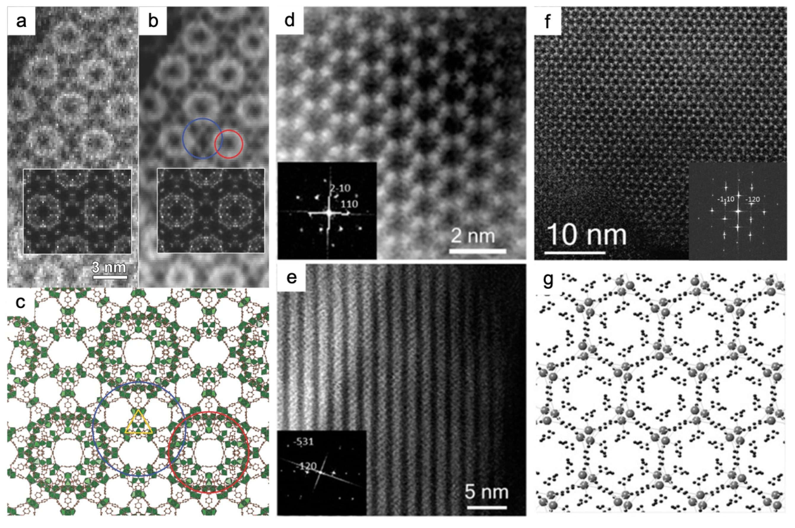
Figure 8.
In-situ LCTEM imaging unravelling formation pathways of ZIF-8(Zn) nanocubes[45] and 2D Hf-MOFs[46] from solution. (a, b) Time series of in-situ LCTEM images (a) and the schematic illustration (b) of the formation process of ZIF-8(Zn). The solution (t = 1 s) phase separates into solute-rich (dark gray contrast) and solute-poor (lighter gray contrast) regions (t = 15 s). The solute-rich regions condense into aggregates (t = 31 s), which then crystallize into ZIF-8 nanocubes (t = 62 s). The red and blue shapes represent Zn2+ ions and 2-methylimidazole (2-Melm), respectively[45]. (c, d) Time series of in-situ LCTEM images (c) and the schematic illustration (d) of the formation process of 2D Hf-MOFs. Hf-clusters assemble into a hexagonal arrangement. The red, blue, and black atoms represent Hf, O and C, respectively. Scale bar, 10 nm[46].
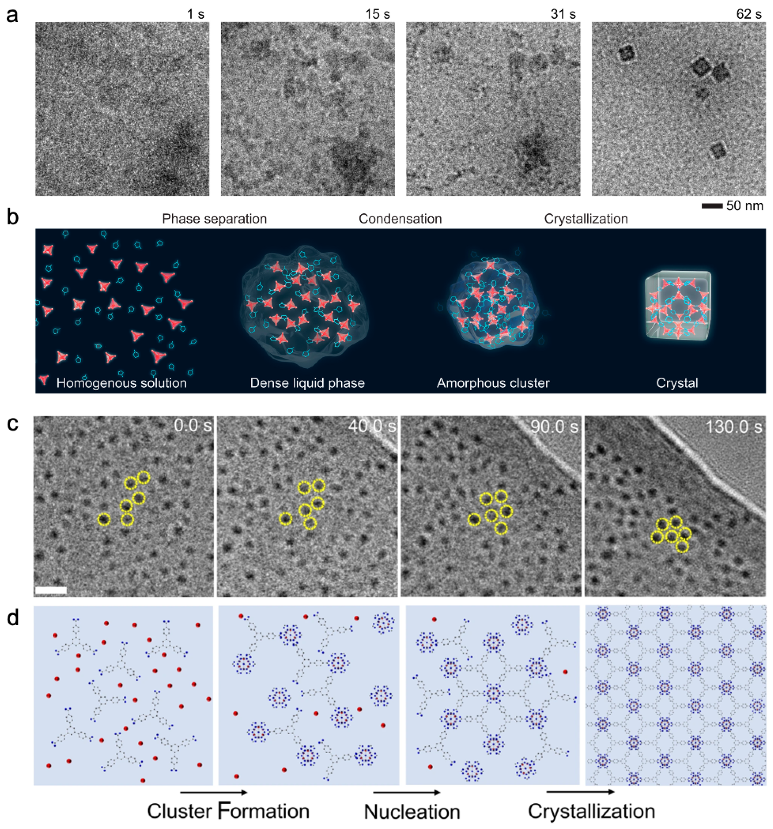
Figure 9.
In-situ structural modification of MIL-101(Cr)[88] and ZIF-8(Zn)[112]. (a-f) In-situ irradiation of MIL-101(Cr) crystals. (a, b) iDPC-STEM images before (a) and after (b) beam irradiation, with mesopores at the edge of crystal marked. Scale bar, 50 nm. (c, d) The zoomed-in view of iDPC-STEM images from the same place with (a, b). Scale bar, 10 nm. (e, f) Yellow boxes between pores with a decrease in contrast indicates the possible displacement of super tetrahedrons[88]. (g-h) In-situ conversion of ZIF-8 nanocubes (g) and rhombic nanododecahedrons (h) into LDH nanocages in liquid phase. Time series of in-situ LCTEM images and corresponding schematic illustration are provided respectively. t0 represents the time point when the etching was first visually detected[112].
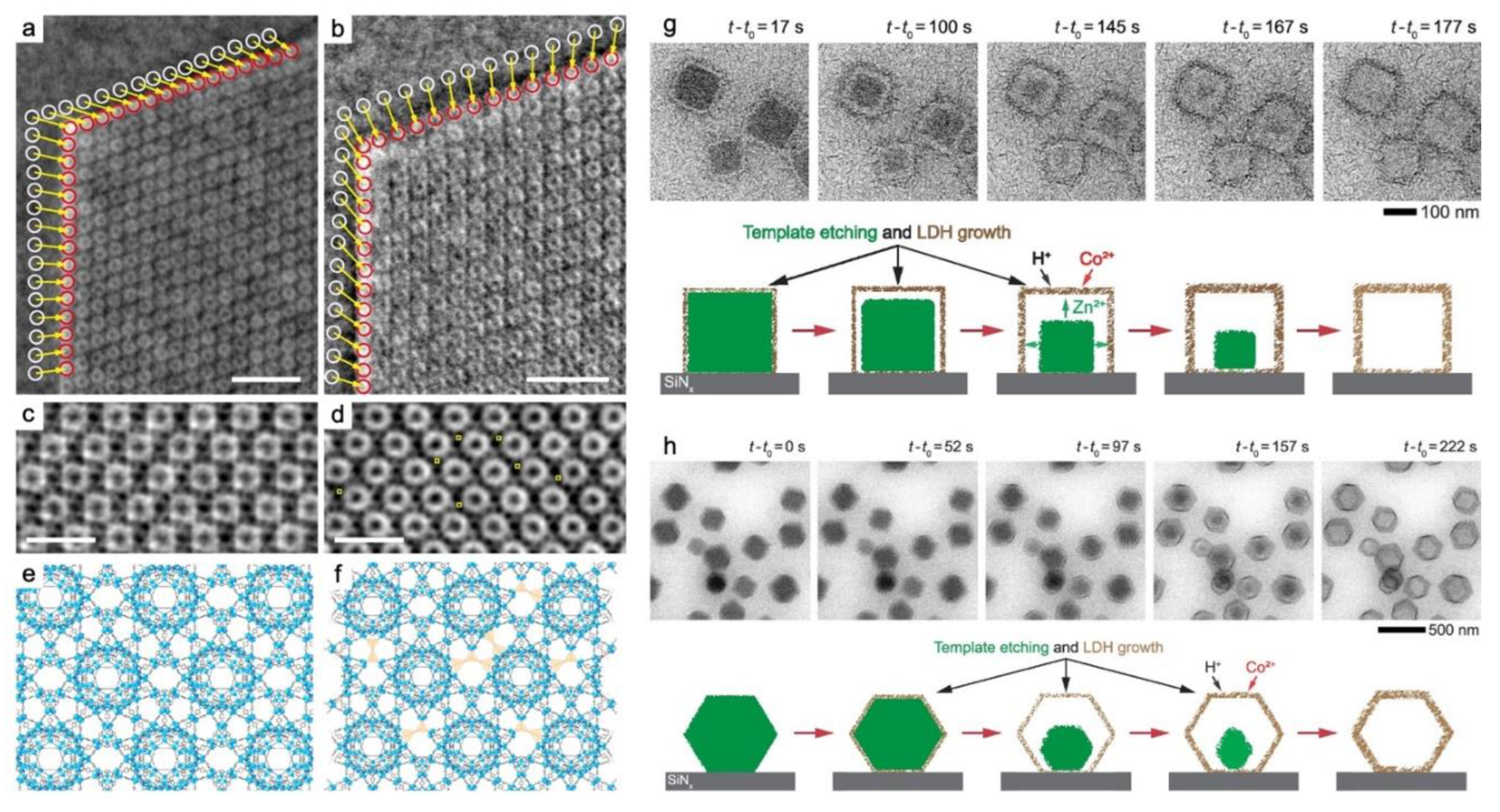

Table 1.
Examples of imaging MOFs using advanced TEM-based techniques.
| Imaging techniques | Advanced cameras | Materials | Accelerating voltage | Temperature | Damage threshold of electron dose | Cumulative electron dose for imaging | Spatial resolution | Imaged structures |
Reference | Year |
|---|---|---|---|---|---|---|---|---|---|---|
| HRTEM | MOF-5(Zn) | 80 kV | Cryo (liquid nitrogen temperature) | Surface | [27] | 2012 | ||||
| HRTEM | 2D Cu2(TCPP) film | 80 kV | Cryo | Bulk | [44] | 2021 | ||||
| HRTEM | DDEC camera | ZIF-8(Zn) | 300 kV | ~25 e- Å-2 | 4.1 e- Å-2 | 2.1 Å | Bulk, surface, interface | [41] | 2017 | |
| HRTEM | DDEC camera | ZIF-8 | 300 kV | ~5 e- Å-2 | Bulk | [25] | 2018 | |||
| HRTEM | DDEC camera | ZIF-8(Zn) | 300 kV | Bulk | [75] | 2018 | ||||
| HRTEM | DDEC camera | ZIF-8(Zn), CO2@ZIF-8(Zn) |
300 kV | Cryo (-170 °C) | ~50 e- Å-2 | ~7 e- Å-2 | Bulk, surface, host-guest interactions | [47] | 2019 | |
| HRTEM | DDEC camera | protein-ZIF-8(Zn) | 200 kV | Cryo | 1 e- Å-2 s-1 dose rate and 5s exposure time) | Nucleation, growth | [48] | 2020 | ||
| HRTEM | DDEC camera | MIL-101(Cr) | 300 kV | ~16 e- Å-2 | ~8 e- Å-2 | 2.5 Å | Bulk, surface | [40] | 2019 | |
| HRTEM | DDEC camera | MIL-101(Cr) | 200 kV | 22 - 32 e- Å-2 | 10 e- Å-2 | Bulk, sublayer surface, surface | [10] | 2020 | ||
| HRTEM | DDEC camera | UiO-66(Zr) | 300 kV | 10 - 20 e- Å-2 | ~12 e- Å-2 | Bulk, surface | [25] | 2018 | ||
| HRTEM | DDEC camera | UiO-66(Zr) | 300 kV | Surface, defects | [14] | 2019 | ||||
| HRTEM | DDEC camera | HKUST-1 | 300 kV | ~6 e- Å-2 | Bulk | [25] | 2018 | |||
| HRTEM | DDEC camera | W doped UiO-66(Zr) | 200 kV | 5 - 10 e- Å-2 | Bulk | [76] | 2018 | |||
| HRTEM | DDEC camera | Mn12Ac@NU-1000(Zr) | 300 kV | Bulk, host-guest interactions | [81] | 2019 | ||||
| HRTEM | DDEC camera | ZIF-L(Zn) | 300 kV | ~ 26 e- Å-2 | Structural modification | [101] | 2021 | |||
| ADF-STEM | MIL-101(Cr), Pt@MIL-101(Cr) | 200 kV | Bulk, surface, host-guest interactions | [84] | 2016 | |||||
| HAADF-STEM | MIL-101(Cr), TiO2-in-MIL-101(Cr) composites |
300 kV | 3.9 Å, 5.2 Å |
Bulk, surface, host-guest interactions | [53] | 2020 | ||||
| HAADF-STEM | MOF-74(Zn) | 300 kV | Bulk | [38] | 2014 | |||||
| HAADF-STEM | MOF-74(Zn) | 300 kV | 2.9 Å | Bulk, surface | [85] | 2015 | ||||
| HAADF-STEM | CsPbI3@ MIL-101(Cr) | 300 kV | Bulk, surface, host-guest interactions | [86] | 2019 | |||||
| HAADF-STEM | MIL-101(Cr) | 300 kV | 54 e- Å-2 | 4.7 Å | Bulk, surface | [88] | 2020 | |||
| HAADF-STEM | ZIF-L(Zn) | 200 kV | ~ 25 e- Å-2 | Structural modification | [101] | 2021 | ||||
| HAADF-STEM | 2D Hf-MOFs | 300 kV | 106 e- Å-2 | Bulk, surface, interface, defects | [46] | 2022 | ||||
| iDPC-STEM | MIL-101(Cr) | 300 kV | ~35 e- Å-2 | Surface | [40] | 2019 | ||||
| iDPC-STEM | MIL-101(Cr) | 300 kV | < 40 e- Å-2 | 1.8 Å | Bulk, surface, interface, defects, nodes and linkers | [18] | 2020 | |||
| iDPC-STEM | MIL-101(Cr), TiO2-in-MIL-101(Cr) composites |
300 kV | 3.2 Å, 3.1 Å |
Bulk, surface, host-guest interactions | [53] | 2020 | ||||
| iDPC-STEM | MIL-101(Cr) | 300 kV | 54 e- Å-2 | 4.7 Å | Bulk, surface | [88] | 2020 | |||
| iDPC-STEM | protein-ZIF-8(Zn) | 300 kV | Cryo | 30 e- Å-2 | Bulk, nucleation, growth | [49] | 2022 | |||
| iDPC-STEM | Pt@UiO-66(Zr), Pd@UiO-66(Zr) | 300 kV | ~4.7 Å | Bulk, host-guest interactions | [92] | 2023 | ||||
| STEM-EELS | DDEC camera | MIL-100(Al), MIL-100(Fe), UiO-66(Zr) |
100 kV | Cryo (125 K) | 10 e- Å-2 | 10 nm (energy resolution: 7 meV) | Chemical information | [94] | 2023 | |
| In-situ TEM: liquid cell |
ZIF-8(Zn) | 200 kV, 300 kV | ~4000 e- nm-2 | Nucleation, growth | [42] | 2015 | ||||
| In-situ TEM: liquid cell |
DDEC camera | ZIF-8(Zn) | 200 kV | 5 e- Å-2 | Nucleation, growth | [45] | 2021 | |||
| In-situ TEM: liquid cell, heating |
Advanced scintillator-based camera | [(L1)Cu2Br2] 1D MOF | 300 kV | Room temperature (23 °C), heating (85 °C) | <10 e- Å-2 | Nucleation, growth | [72] | 2019 | ||
| In-situ TEM: liquid cell |
DDEC camera, advanced scintillator-based camera | Ag-1D MOF | 300 kV | 70 e- Å-2 | Nucleation, growth | [96] | 2020 | |||
| In-situ TEM: liquid cell, heating |
DDEC camera, advanced scintillator-based camera | NU-906, NU-1008 |
300 kV | Room temperature, heating (80 °C) | < 6 e- Å-2 | Bulk, phase transition | [97] | 2020 | ||
| In-situ TEM: ETEM (gas) |
Advanced scintillator-based camera | H2O@MIL-53(Cr) | 300 kV | Room temperature (27 °C), heating (800 °C) | ~ 5 e- Å-2 | Pore breathing | [100] | 2017 |
Disclaimer/Publisher’s Note: The statements, opinions and data contained in all publications are solely those of the individual author(s) and contributor(s) and not of MDPI and/or the editor(s). MDPI and/or the editor(s) disclaim responsibility for any injury to people or property resulting from any ideas, methods, instructions or products referred to in the content. |
© 2023 by the authors. Licensee MDPI, Basel, Switzerland. This article is an open access article distributed under the terms and conditions of the Creative Commons Attribution (CC BY) license (http://creativecommons.org/licenses/by/4.0/).
Copyright: This open access article is published under a Creative Commons CC BY 4.0 license, which permit the free download, distribution, and reuse, provided that the author and preprint are cited in any reuse.
Submitted:
20 April 2023
Posted:
21 April 2023
You are already at the latest version
Alerts
A peer-reviewed article of this preprint also exists.
This version is not peer-reviewed
Submitted:
20 April 2023
Posted:
21 April 2023
You are already at the latest version
Alerts
Abstract
Metal-organic frameworks (MOFs), composed of metal nodes and inorganic linkers are promising for a wide range of applications due to their unique periodic frameworks that can be flexibly tuned. Understanding of the structure-activity relationships can facilitate the development and application of MOFs nanomaterials. Transmission electron microscopy (TEM) is a one-of-a-kind technique capable of characterizing MOFs microstructures at the atomic scale. Besides, in-situ TEM set-ups make it possible to direct visualize the microstructural evolution of MOFs in real time, which enables monitoring transitions of MOFs during growth as well as under working conditions. However, MOFs are so sensitive to the high-energy electron beam which makes TEM-based characterizing methods challenging. In this review, we first introduce the main damage mechanisms for MOFs under electron beam irradiation and two strategies to minimize the damages: low-dose TEM and cryo-TEM. Then, we discuss the techniques combined with the two strategies to analyze the MOFs’ microstructure, including three-dimensional electron diffraction, direct detection electron counting camera, and iDPC-STEM. Groundbreaking milestones and research advances with respect to static characterization of MOFs structures are highlighted. In-situ TEM studies are exemplary reviewed to provide insights into MOFs dynamics induced by various stimuli. Additionally, perspectives on promising techniques that may further facilitate the MOFs study using TEM are analyzed.
Keywords:
Subject: Chemistry and Materials Science - Materials Science and Technology
1. Introduction
Metal-organic frameworks (MOFs) are porous crystalline materials comprised of inorganic metal ions or clusters and organic ligands [1]. As a unique class of materials featuring tunable topologies, large specific surface area, high porosity, adjustable chemical compositions, and functionalities, MOFs are promising candidates for catalysis [2], gas storage and separation [3,4], energy storage and conversion [5], chemical sensing [6], water adsorption [7], and lithium-ion storage [8], etc. Structure-activity relationships guide rational development and applications of flexible and functional MOFs. The determination at the atomic scale of the crystal structures and the mechanisms of structural evolution under realistic working conditions is a well-founded prerequisite for understanding the relationships.
Surface, interface, defect, and host-guest interaction are the main microstructures, which affect directly the MOFs’ properties. Considering practical applications, modification of surface is an important means of MOFs’ functionalization [9]. Surfaces have an impact on surface-related properties and growth processes [10]. Interfaces are of great significance between MOFs crystals or with other materials for plasma crystals, composites, MOF-based devices, among others [11-13]. Defects provide a method to locally adjust porosity and create active open metal sites for MOFs [14,15], which allows defect engineering for the specific function [16]. Defects can be introduced artificially under control for modifications [17], or be generated spontaneously during the assembly process [18]. Due to distinguished porous nature and long-distance orderly structure, MOFs crystals with interconnected rigid networks are ideal framework materials to provide regular and regionally large accommodations for guest species including ions, particles, clusters, and molecules [19-21]. Host-guest controllable incorporation and synergetic interactions allow for their applications [22,23]. To enhance the utilizations MOFs, thorough understanding of the growth and transformation mechanisms, as well as the evolution pathways of MOFs under working conditions are crucial in addition to the inherent properties of the static structure.
Among characterization techniques, transmission electron microscopy (TEM) is undoubtedly suitable, given the ability of high-energy electrons to interact with thin specimens. Apart from structural analysis via electron diffraction, both TEM mode and scanning transmission electron microscopy (STEM) mode permit direct imaging regions of interest in the specimen, including its periodic, non-periodic, local, and porous details inside and on the surface of MOFs at the atomic scale. Meanwhile, TEM is capable to be combined with spectroscopic techniques to examine the chemical elements. Moreover, using novel in-situ sample holders, TEM can introduce real-time external fields and conditions such as low temperature, heating, biasing, liquids, gases, etc., enabling on-demand scenarios of the sample in practical applications.
However, MOFs are difficult to stabilize under the high-energy electron beams due to their organic components and the coordination bonds that connect organic parts to the metals. The fundamental hinderance to analyzing MOFs using TEM is their extreme sensitivity to electron beam irradiation, which causes either the structural disintegration before detection finishing or the lack of intrinsic characteristics during acquisition [24,25]. Hence, the nature of MOFs weakens the feasibility and merits of research using TEM. It is essential to update TEM-related methods and techniques to be appropriate to beam-sensitive materials. To this end, the idea of low electron dose and low temperature was established for the consideration of damage mechanisms in MOFs [26,27]. Multiple advanced TEM techniques were developed, which primarily include three-dimensional electron diffraction (3DED), direct detection electron counting (DDEC) camera, and integrated differential phase-contrast scanning transmission electron microscopy (iDPC-STEM) imaging [28-30].
Several review articles have discussed the works on studying MOFs using TEM. Huang et al. summarized the development of 3DED methods and demonstrated their capabilities for MOFs’ structural characterization [31,32]. Wiktor et al. [33] and Liu et al. [34] presented the problems and approaches of MOFs’ research by TEM, and the advances in terms of structural characterization of MOFs up to that time. Apart from these aspects, Gong et al. [35] and Zhang et al. [36] discussed new findings based on in-situ TEM methods afterwards. Nevertheless, no articles have comprehensively proposed the scope of applicability of diverse TEM-related techniques for probing MOFs materials from the perspective of the theoretical principles and practical operations. Herein, we discuss the challenges, strategies, and advanced techniques for MOFs research based on TEM, and introduce representative research advances in structural analysis and dynamic evolution. We demonstrate the practicability and indispensability of TEM as a powerful tool in this field. Meanwhile, some perspectives on cutting-edge TEM-based techniques which are potential for MOFs study have been proposed.
2. Challenges and chances of TEM studies
MOFs are so unstable and sensitive to the high-energy electron beam featured in TEM, which makes the structural characterization of MOFs challenging. This necessitates knowledge of the electron beam damage mechanisms in MOFs.
2.1. Damage mechanisms
Radiation damage mechanisms of MOFs under the high-energy incident electron beam mainly include radiolysis, knock-on damage, and thermal effects [25]. In practical situations, the determination of the predominant mechanism can help find the proper method to minimize damage [24].
The radiolysis (or ionization damage) is electron-electron interaction-induced ionization of specimen atoms via inelastic scattering that results in chemical bond weakening or breakage, phonon scattering, etc. It is the primary cause of MOFs degradation as reported, especially at lower voltages. This beam damage can be eased by high-energy incident electrons because they lead to fewer inelastic scattering events. However, the signal-to-noise ratio of image and spectrum is unimproved because both the inelastic and elastic cross-sections are inversely proportional to incident energy [37]. Low temperature effectively improves the beam stability of the specimen and mitigate radiolysis, which can be realized at cryogenic temperatures by using liquid nitrogen or helium (cryo-TEM) [24,27].
The knock-on damage originates from direct electron-nucleus interaction, specifically the atomic displacements or sputtering in the original specimen caused by high-energy electrons. Low-energy incident electrons prevent knock-on damage, whereas at the cost of weak beam penetration depth and poor signal resolution[25]. Reduction of the TEM accelerating voltage below the sample-specific threshold value while maintaining the resolution (low-voltage TEM) is an alleviation method.
The thermal effects (or beam heating) arise from electron-atom interaction-induced collective crystal lattice vibration, and can be mitigated by lowering the incident-beam current [37]. This damage can be mitigated to some extent by cryogenic temperatures.
2.2. Strategies for minimizing damages
Principles for structural maintenance when probing the static structure and dynamic behavior of MOFs by TEM without damaging the intrinsic properties can be broadly divided into two parts: low-dose TEM and cryo-TEM.
2.2.1. Low-dose TEM
Given that all these electron beam-induced irradiation damages are dose-related, reduction of the electron dose (low-dose TEM) is a general solution applied to MOFs regardless of the damage mechanism. A pre-evaluation is required to determine whether the low-dose conditions are within the acceptable range to maintain the stability of crystallinity. Electron diffraction (ED) is an effective and feasible way to determine the electron dose that the MOF can withstand, partly because it can be performed at low doses. As the electron dose increases, changes in the ED patterns mean modifications in the structure, i.e., the appearance of disordered phases. Shorter exposure time and lower intensity contribute to achieving low electron dose conditions [26]. The maximal electron dose that MOFs can withstand depends on materials and respective TEM operating conditions. Take typical MOFs in TEM mode under 300 kV accelerated electron beam as examples, the electron dose that MIL-101(Cr) can withstand is ~16 e- Å-2 [40]. The onset of beam damage for UiO-66(Zr) was from 10 to 20 e- Å-2 [25], and ZIF-8(Zn) about 25 e- Å-2 [41]. Compared to static characterization, in-situ TEM studies require longer irradiation time, which necessitates an electron dose considerably below the damage threshold to ensure the integrity of the sample region of interest during dynamic processes. In the liquid cell TEM (LCTEM) observations of UiO-66(Zr) and ZIF-8(Zn), the cumulative electron flux of ~20 times less than the threshold was considered appropriate [42].
2.2.2. Cryo-TEM
Cryo (low-temperature) concepts can be introduced to MOFs to probe structural details without collapse because they are able to preserve the native state and extend the irradiation time span, although there is a limit to the reduction of degradation caused by heating [25,27]. For example, at 120 K, the structures of the highly porous CAU-7(Bi) were characterized by ED [43]. At liquid nitrogen temperature, the complete pore structure and the periodicity of the crystal lattice of MOF-5(Zn) nanocrystals were imaged by high-resolution TEM (HRTEM) [27]. Cryogenic temperatures also enable the elucidation of the orderly internal architecture of large-area conductive 2D Cu2(TCPP) (TCPP = meso-tetra(4-carboxyphenyl)porphine) films on dielectric substrates by HRTEM and ED [44].
Apart from minimizing structural damage and improving electron tolerance during characterization, cryo-TEM also helps stabilize and preserve specimens at the status of interest during an in-situ TEM observation. Examples include in-situ studies on the crystallinity of MOFs in the liquid phase at specific reaction stages [45,46] and the construction of MOFs after interaction with gas species [47]. For the latter, two preferred adsorption sites for CO2 were discovered to be the centers within 6-ring channels and 4-ring channels, supported by HRTEM performed at -170 °C and with a cumulative electron flux of ~7 e- Å-2 using a DDEC camera. The unit cell of ZIF-8(Zn) expanded by ~3% due to molecular guests (Figure 1a–d) [47].
In addition, cryogenic conditions are applicable to the biological field, such as biomacromolecule-metal-organic frameworks (biomacromolecule-MOFs). For protein-ZIF-8(Zn), the amorphous precursor phase in the nucleation was directly observed, revealing a non-classical nucleation approach of dissolution-recrystallization and protein-rich amorphous solid phase transformation [48]. Furthermore, under cryogenic settings, the difference in atomic-level nanoarchitectures, which significantly affected the bioactivity and was caused by different crystallization pathways in synthetic scenarios, was unraveled for the first time. For BZIF-8-S, heterogeneously crystallized by solid-state transformation of the biomacromolecule amorphous phase at the spontaneously growing ZIF-8 crystal surface, the crystal structure with regularly narrow pore windows hindered the diffusion of the catalytic substrate. For BZIF-8-B, crystallized around surface directly via electrostatic interaction with the induction of biomacromolecules, slow crystallization rate with an observable amorphous phase as well as defects enhanced the bioactivity (Figure 1e–g) [49].
Figure 1.
HRTEM characterization under cryogenic conditions of CO2@ZIF-8(Zn)[47] and protein-ZIF-8(Zn) composites[49]. (a-d) Host-Guest Structures within ZIF-8(Zn) viewed along [111] (a, b) and [001] (c, d) projection. (a, c) Left: CTF-corrected Cryo-TEM images of CO2-filled ZIF-8 particle taken with electron dose rate of ∼4.5 e- Å-2 s-1 for 1.5 s. Bright regions correspond to mass density, and contrast in the center of the 6-ring window (a) and 4-ring window (c) is observed respectively for multiple unit cells. Middle: magnified image of a single ZIF-8-unit cell. Density at the center indicated by red arrows likely corresponds to CO2 adsorbed within ZIF-8. In (c), only the pore cavity at the vertices of the 4-ring window contains this density. (b, d) Simulated structure of ZIF-8 with DFT-predicted binding site of CO2 indicated with red spheres in (a, c), respectively[47]. (e-g) iDPC-STEM images, corresponding FFT, and the structural analysis of the selected area (indicated with the same color) of BZIF-8-S from the [111] (e) and [100] (f), and BZIF-8-B from the [111] (g) zone axis. (e, f) show high-crystallinity with ~3.4 Å 6-ring window and ~2.8 Å 4-ring window, respectively. (g) shows crystalline and amorphous phase, and coordination defects[49].
3. Strategies, techniques, and research advances
3.1. Traditional and Advanced electron diffraction
Large MOF crystals are occasionally difficult to prepare, and frequently, only nano- or submicron-sized crystals can be manufactured based on reaction kinetics and thermodynamics. Electron diffraction (ED), because of its ability to probe nanosized crystals, is better suited for structural investigations of MOFs than conventional X-ray diffraction (XRD) which is ideal for atomic-scale analysis of large crystals (at least microns in size) [50]. ED is preferable to HRTEM because it requires a lower dose of electrons to achieve the same level of resolution, if the resolution and observed region meet the practical requirements. This supports the use of ED to determine the maximum amount of electron flux that MOFs can withstand. For instance, ED reviewed ZIF-8(Zn) crystals with enough contrast at a dose rate of only ~1 e- Å-2 s-1 [41]. ED requires tilting the crystal along specific zone axes in order to obtain accurate structural information. However, beam-sensitive MOFs suffer from the time-consuming process of collecting a few ED patterns along precisely aligned crystallographic zone axes. The challenge of accurately describing the crystal structure by ED also lies in the method of merging multiple ED maps, which requires the correct handling of multiple scattering effects [51]. Therefore, the limitations are primarily related to the data collection strategy.
Three-dimensional electron diffraction (3DED) enables the effective collection of ED data and subsequent ab initio structure determination and analysis [28]. The 3DED data set of a single crystal is a sequence of ED patterns recorded sequentially at different tilt angles of the TEM goniometer, which then produce corresponding diffraction peaks (Figure 2a) [32]. This technique so far has evolved from stepwise strategies to the faster continuous strategies from a data collection perspective.
Among the former type, electron diffraction tomography (EDT) was first proposed in the late 2000s [52]. The program-controlled TEM sample stage automatically records the stepwise tilt angle relative to the electron beam and collects the rotational motion of the ED patterns. Apart from MOFs themselves, the EDT technique has also been applied to the distribution of guests in MOFs, such as TiO2 in MIL-101(Cr) mesopores [53]. To decrease the required electron beam intensity, automatic diffraction tomography (ADT) combined with precession electron diffraction (PED) equipment was designed later to control tilt angles of goniometers. This protocol improves the analysis of porous and organic sub-microcrystalline samples at the single-crystal scale, but operate entirely in STEM mode [52,54,55]. Using ADT and a cryo-TEM holder, bismuth-based MOF Bi(BTB) (BTB=1,3,5-benzenetrisbenzoate) (also denoted as CAU-7) was reconstructed, and the law of triple twinning of pseudo-hexagonal symmetry growth of the rod-shaped aggregates was proposed.[43]. Compared to the PED method, which is suitable for the near-kinematical data collection from single zone axes, rotational electron diffraction (RED) contributes to the complete collection of 3DED data and reconstructs the reciprocal space with high resolution [56]. In addition to the goniometer tilt controlled by ADT, RED combines fine electron beam tilt so as to further accelerate data collection and eliminate the need for precise alignment to specific zone axes. RED assisted in the direct determination of the pore structure of UiO-66(Zr), which was further confirmed by Rietveld refinement of XRD [50].
The latter type of strategy enables crystals to be rotated continuously to speed up data acquisition and simultaneously obtain relatively accurate and complete ED intensities as a movie. This type improves on the previous one by limiting the goniometer tilt and is particularly suitable for crystals with low symmetry. Continuous rotation electron diffraction (cRED) has elucidated structures of several types of MOFs and has always been confirmed or supplemented by relatively ambiguous XRD data in reported works. Examples include atomic positions of Ti8Zr2O12(COO)16 cluster-based PCN-415 and PCN-416 [57], and lattice of TiVI 4,4’-biphenyldicarboxylate (bpdc2-) MOF termed COK-47 [58], Zr chain-based PCN-226 [59], ZIF-EC1(Zn, Co) [60]. UU-100(Co) was unraveled to have a tetrahedral unit cell with the lattice parameters a = b = 27.3 Å and c = 19.6 Å, a possible P4/mbm space group, and rectangular channels with elliptical pores [61]. Despite the current rarity of high conductivity in MOFs, MOFs are welcomed in fields such as electrocatalysis and charge storage because of their porous structures [62]. Electrically conductive 2D MOFs have attracted attention for their hexagonal 2D lattices like 2D van der Waals stacked materials. In regard to a class of 2D π-conjugated MOFs, the structure details of M3HHTT2 (HHTT = 2,3,7,8,12,13-hexahydroxy tetraazanaphthotetraphene, M = Cu2+ or Ni2+) with a resolution of ~1.5 Å verified convincingly the π-stacking by an interlayer distance of 3.19±0.02 Å, which results in rare eclipsed AA stacking [63]. Crystal tracking was developed to resolve the issue of likely divergence of crystals from the selected regions during continuous rotation by defocusing every few ED patterns [64]. Micro-electron diffraction (MicroED) is a technique that uses an ultra-low electron dose at cryogenic temperatures and is similar in principle to PED [65,66]. It has been extended from biomacromolecules to the beam-sensitive materials, as exemplified by the structure of ZIF-8(Zn), which was determined to be 0.87 Å from a single nanocrystal and compares well with XRD results [67]. Notably, the environmental 3DED method in combination with continuous 3DED and environmental TEM (ETEM) has been proposed and validated for single microcrystals to study the structural dynamics under external stimuli. The atomic-level ab initio structure determination of MIL-53(Al) under vacuum, cryo, heating, gas, and liquid conditions was conducted (Figure 2c) [68]. Thus, it was demonstrated that in-situ ED, as an in-situ TEM-based approach, can also be used to analyze the dynamic behaviors of MOFs placed in external fields [68].
Figure 2.
Advanced electron diffraction: three-dimensional electron diffraction (3DED)[32,68] and scanning electron diffraction (SED)[15]. (a) The data collection procedure of 3DED. Green: obtained data; pink: missing wedges; blue cube: target crystal; blue arrow: rotation direction; yellow arrow: incident electron beam[32]. (b) Illustration of SED applied to a defect-engineered UiO-66(Hf) particle. A 2D (kx, ky) diffraction pattern is recorded in transmission at every probe position in a 2D (x, y) scan[15]. (c) ETEM images (top), ETEM 3DED data (middle), and determined structures (bottom) of MIL-53(Al) single crystals under different conditions. Particles marked with blue dashed lines (top) were used for collecting 3DED data. White circles in diffraction data (bottom) represent a resolution of 1 Å. The 3DED data are projected along the [010] (i-iii) and [001] (iv, v) directions of the samples: the as-made phase (MIL-53as), the high-temperature phase (MIL-53ht) and the H2O-containing phase (MIL-53lt, room temperature, in the air). (i) MIL-53lt-cryo: the low temperature phase prepared by plunge-freezing and cryogenic transfer protocols. (ii) MIL-53lt-gas (air): MIL-53lt in the static air (0.1 MPa). (iii) MIL-53lt-liquid (H2O): MIL-53lt covered with liquid water. (iv) MIL-53as-v: the as-synthesized phase MIL-53as under high vacuum state. (v) MIL-53as-ht-v: the phase after calcination of MIL-53as at 603 K and high vacuum for 2 h[68].
Conventionally, ED is only applicable to reveal spatial average information, including periodic crystal structures or abnormal macroscopic features. It is represented by revealing the reo topology with the existence of missing cluster defects of UiO-66(Hf) via multiple diffraction behaviors, including ED [17]. Direct imaging methods in TEM mode or STEM mode are always required to resolve local non-periodic structures such as surfaces, interfaces, defects, guest molecules, etc., which are equally important. Organic molecules in pores were for the first time located using cRED with a resolution of 0.83-1.00 Å, in the study of Co2(Ni-H4TPPP)]·2DABCO·6H2O (DABCO = 1,4-diazabicyclo[2.2.2]octane) denoted by CAU-36 at 96 K [69]. Hydrogen atoms in ICR-1, ICR-2, and ICR-3 based on the ligand PBPA (phenylene-1,4-bis(methylphosphinic acid)) were positioned by full dynamic diffraction theory in the least-squares refinement of the EDT [70]. Besides, the emerging technique, scanning electron diffraction (SED) based on the 4D-STEM, has been proposed to compensate for the limitations of ED (Figure 2b) [15]. The size, morphology, local orientation, and spatial distribution of defect nanodomains reo of single-crystal UiO-66(Hf) octahedral particles were directly reflected by two-dimensional diffraction patterns scanned on every part of the entire sample, with a spatial resolution of 2-5 nm realized by a focused electron probe with a convergence angle of about 1mrad. The blocky lamellar morphology caused by the local fluctuation of phthalate concentration preferentially extended in a direction perpendicular to the {111} crystal plane, and there were interfaces between the reo and fcu domains on the {211} plane. Despite the progress made, the inherent deficiency of ED in probing local structures makes imaging in TEM and STEM modes still an indispensable tool in the study of MOFs materials.
3.2. TEM and DDEC camera
The ability of TEM imaging to directly visualize atomic-scale information has been greatly improved owing to the advancement of spherical aberration (Cs) correctors and contrast transfer function (CTF) correction techniques [14,71]. In terms of minimizing the electron dose during imaging, an efficient way to enhance the camera data acquisition is to use highly sensitive scintillators and fiber optics, which allow the detection of signal electrons with a high signal-to-noise ratio. This approach has been used in observations of MOFs [48,72]. However, conventional cameras convert the photons generated by the action of the electrons and scintillators and received by the optical fiber guide into an electrical signal. The conversion process consumes a significant portion of the electrons which are essential for imaging. While having great imaging capabilities as techniques advance, these cameras lack the sensitivity needed to collect high-quality data at a very low electron beam dose.
The DDEC camera is considered to have ultra-high quantum detection efficiency due to its ability to directly detect electronic signals without undergoing the signal conversion process described above [73]. Therefore, with the ability to detect low-dose electrons, the DDEC camera contributes to directly forming the phase contrast image of the lattice planes, pores, and surfaces of the coherent interfaces with good speed and sensitivity, which is especially suitable for low-dose and real-space imaging of hybrid materials [74]. With the ultrahigh readout speed of the DDEC camera, it is possible to record nanoscale phenomena in real time at the microsecond to millisecond level and investigate the atomic details of local structures, opening up the potential for in-situ studies and accurate structural analysis. However, the DDEC camera has high requirements on the electron dose to prevent the devices from breaking at high doses.
The octahedral MIL-101(Cr) was almost the first typical MOF whose structures were investigated by TEM [39] and structural details were further elucidated more thanks to the advanced techniques. Under Cs and contrast transfer function (CTF) correction under low-dose conditions, the highly ordered medium-sized cage stack HRTEM images of MIL-101(Cr) were collected with a resolution of 2.5 Å were collected at 4,000-fold magnification. Each image stack is composed of 120 frames and each frame had an exposure time of 0.05 s, which corresponds to a total exposure time of 6 s, but the total electron dose was only ~8 e- Å-2 [40]. Subsequently, the existence of the sublayer surfaces of MIL-101(Cr) was confirmed by the compelling evidence at the atomic scale. The sublayer surfaces terminated by inorganic Cr3(μ3-O) trimers underwent the transition to stable {111} surfaces regulated by inorganic polynuclear nodes [10]. For ZIF-8(Zn) with highly ordered and oriented macropores, the single crystalline nature of an ideal sample was confirmed by HRTEM (Figure 3a–c) [75]. Also by virtue of the HRTEM image captured by DDEC camera, the crystallinity retention and the pore structure of the UiO-66(Zr) nano-cage single crystal doped with WO42- ions were verified to be distinguishable and clear after the fine collapse. Pore size could be adjusted in the range of 80-140 nm by the ion dose of the etching reaction [76].
The surface and interfacial structures of MOFs particles exert impacts on mechanisms of molecular assembly, which affect the morphologies and structures. Under Cs and CTF correction and using a DDEC camera, TEM images of ZIF-8(Zn) were acquired at an ultra-low dose of ~4.1 e- Å-2 and a high frame rate of 40 fps (120 frames in the exposure time of 3 s). The spatial resolution of 2.1 Å was sufficient to resolve the single atomic arrangement of Zn and organic linkers in the framework [41]. The terminations of the {110} surfaces were consistent with the armchair model without reconstruction or macro-defects [41], while those of the {011}surfaces were caused by doubly coordinated Zn clusters connected to two other clusters [47]. For surface terminations of UiO-66(Zr), ligand-free and ligand-capped surfaces were revealed to be coexisting: the major exposed {111} surface terminates with BDC linkers, and the small truncation surface exposes Zr clusters at the kink positions between {100} and {111} facets (Figure 3d–f) [25]. With regard to the HRTEM resolution capability aided by DDEC cameras for interfaces, a {110} coherent interface was verified to form between two assembled ZIF-8(Zn) crystals driven by van der Waals attractions or dipole-dipole interactions. An additional layer of extra ligands existed in the interface, suggesting no chemical reactions in the direct adhesion of two ligand-terminated surfaces [41]. In short, TEM probes the surface structures of MOFs, from the mere detection of surface steps to the identification of metal clusters, then to the discrimination between metal nodes and organic linkers. The coordination of nodes and linkers can be studied through the TEM characterization of the local structure, for example, UiO-66(Zr) [25] and ZIF-8(Zn) [41], which favors the further study of the MOFs’ structure-function relationship[18].
A combined technique of low-dose TEM and electronic crystallography was developed to discover that the ordered “missing linker” and “missing cluster” (Figure 3g–l) coexist in UiO-66(Zr) at sub-Å resolution. The “missing linker” defects underlay a topology of bcu net owing to the defect-terminating formate ligands, and were notably identified for the first time. High quality HRTEM images were essential to unambiguously resolve all structural components by 3D reconstruction. This type was prevalent and robust with prolonged crystallization time and crystal ripening. The “missing cluster” defects were categorized into reo and scu structures by the presence or absence of the face-on BDC linkers surrounding but not connected to the missing clusters. This type appeared only in small regions with few units of cell size and tended to disappear over time, but was more catalytically active. The catalytic activity of UiO-66(Zr) was proposed to be enhanced by the understanding of the defect characteristics and the newly-developed techniques to control the evolutionary tendencies [14].
In the early days, the characterization of host-guest systems inevitably involved structural decomposition. However, HRTEM alone or assisted by ED was sufficient to confirm the feasibility of the loading method, as well as the size, residing location, monodispersity, and anchoring stability of the guest loaded on the host. For the guests with typical size in the range of 1-5 nm, study cases include Cu@MOF-5 [77], Ru@MOF-5 [26], Pd@MOF-5 [26], Pd@MOF-177 [78], Pd@MIL-101 [79], Pd@HKUST-1 [80], and Au@ZIF-90 [20]. Electron tomography made the guests’ distribution within the hosts clearer, preventing surface bias and other factors from skewing the results.[20,26] As technologies evolve, the integrity of the host and guest can be preserved while imaging structural details. For example, the cryo-TEM strategy enabled the characterization of host MOFs encapsulating gas molecular guests [47]. Single-molecule magnet (SMM) is a promising guest species for MOFs. Nanostructured organization and nanoscale protection in a two-dimensional or three-dimensional network are required to achieve the reading and writing process for its potential application in the next generation of computing technology related to molecular spintronics. Using a DDEC camera, HRTEM directly imaged the Mn12O12(O2CCH3)16(OH2)4 (denoted as Mn12Ac, a kind of SMM) molecules with a uniform size of ~2 nm that were encapsulated in a mesoporous NU-1000(Zr). The adsorption of isolated molecular guests within hosts was demonstrated for the first time (Figure 3m–o) [81].
Figure 3.
HRTEM imaging of ZIF-8(Zn)[75], UiO-66(Zr)[14,25] and Mn12Ac@NU-1000(Zr)[81] using DDEC cameras. (a-c) Bulk of ZIF-8(Zn) with single-crystalline nature at different magnifications taken along the [011] zone axis. The inset of (a) shows the corresponding ED patterns, and the inset of (b) shows the indexed FT patterns. (b) and (c) are magnified views of the white square areas in (a) and (b), respectively[75]. (d-f) A truncation surface in a thermally treated UiO-66(Zr), showing crystal growth steps involving small {100} (labeled in blue) facets and {111} facets (labeled in yellow). (d) The white arrows point “kink” positions between {100} and {111} facets. (e) Ligand-terminated {111} surface: (left) structural model, (middle) HRTEM image by real-space averaging; (right) the averaged image in rainbow colors to increase the visibility of the ligand contrast. (f) Metal-terminated (ligand-free) {100}/{111} kink: (left) structural model; (middle) HRTEM image by real-space averaging; (right) the averaged image in rainbow colors[25]. (g-i) Missing linker defects and missing cluster defects in UiO-66(Zr). (g-j) Missing linker defects. CTF-corrected HRTEM images in column (i) and the projected structural model (Zr, cyan; O, red; C, grey; H atoms) in column (ii) along the [001] (g), [100] (h) and [110] (i) zone axes. Scale bars, 2 nm. (j) The reconstructed 3D electrostatic potential map viewed in two different orientations, showing an 8-connected network with the Zr6O8 clusters, BDC linkers and defect-terminating ligands (formates), with H atoms omitted for clarity. (k, l) Missing cluster defects viewed from the [001] direction, adopting the reo (k) and the scu structure (l). Column (i) show CTF-corrected HRTEM images and column (ii) shows the projected structural model (Zr, cyan; O, red; C, grey; H atoms). Scale bars, 5 nm[14]. (m-o) Guest species and host MOF: Mn12Ac@NU-1000(Zr). (m) HRTEM image and ED pattern (inset) of Mn12Ac@NU-1000 acquired along the [001] zone axis of NU-1000. Arrows point to the Mn12Ac clusters. (n, o) Enlarged images of the highlighted areas in areas 1 and 2 in (m), respectively. Mn12Ac clusters are shown to be encapsulated and fitted in the hexagonal channels of NU-1000(Zr)[81].
For minimization of the electron beam irradiation, fast seeking of the zone axis is essential for the DDEC camera. The time-consuming process of switching back and forth between imaging and diffraction modes in the traditional manual method results in the passive and undesirable acceptance of hundreds of electrons per Å2. A program [25] was developed to achieve a direct and one-step alignment of the zone axis for crystals whose initial orientations are close to the zone axis within 5° with a total dose well below 1 e- Å-2. This was conducted by calculating tilt angles from Laue circles identified from off-axis ED patterns. Additionally, when using a DDEC camera, the technique of dividing the exposure into stacks of sequential short-exposure frames to reduce the effects of electron beam-induced specimen motion requires the precise elimination of drift between frames. To address this, an "amplitude filter" was developed to limit the phase analysis to "reliable" high amplitude pixels [25]. This program contributed to the detection of organic linkers with lower atomic numbers on the surface of UiO-66(Zr).
In addition, the thickness effect is important for the phase contrast image captured by the DDEC camera, especially for the inorganic samples that are sensitive to irradiation. It is often necessary to have a simulation or image that directly corresponds to the position of the atoms and the contrast for an accurate interpretation.
Novel DDEC cameras, which allow direct imaging of MOFs at very low electron doses due to their high quantum detection efficiency, are a huge boost for HRTEM, enabling nondestructive visualization for MOFs materials under well-controlled conditions (Table 1). Nevertheless, HRTEM images taken with DDEC cameras still require a series of defocused images as those taken with scintillator-based cameras for a reasonable image correction and interpretation. The low-electron dose basic principle required by MOFs presents a challenge in determining Scherzer defocus, an issue that the DDEC cameras are not yet able to overcome.
3.3. Traditional STEM and iDPC-STEM
In terms of interpretation for high-resolution images, the coherent electron beam for TEM mode results in contrast reversion with defocus. It is necessary to determine the true structural information through a series of defocused images and subsequent analysis based on crystallographic principles. With a convergent electron beam, STEM mode has a higher resolution due to incoherent phase scattering imaging. Bragg diffraction exists only in the low angle bright-field (BF) and annual dark-field (ADF) imaging modes. The contrast of ADF images is proportional to the one-third power of the atomic number. The high-angle annual dark-field (HAADF) mode produces Z-contrast images, in which the contrast is proportional to the square of the atomic number. Due to the small scattering angle, elements with low atomic numbers are challenging to image. Nevertheless, STEM images are convincing to directly identify elements with a relatively obvious difference in contrast between them in the sample.
Therefore, the STEM mode has obvious advantages over the traditional TEM mode for its ability to accurately image non-periodic local structures such as defects, boundary surfaces, and deformations in crystals [18,74,82,83] and to analyze chemical elements.[26] Cs correctors also enhance the spatial resolution of the STEM mode [71].
The pore structures and super-tetrahedron building blocks of MIL-101(Cr) were observed using ADF-STEM with the beam current of <10 pA and the convergence semiangle of 22 mrad, which validated the controlled synthesis of a well-defined morphology (Figure 4a–c) [84]. With the probe size of 0.8 Å, and the beam current of <1.65×10⁻¹⁰A using a convergence semiangle of 17 mrad, the HAADF images permitted for the first time "quasi" atomic resolution imaging for nanometer MOF-74(Zn) prepared at room temperature (Figure 4d,e) [38]. The Zn clusters arranged in a hexagonal distribution were identified according to the bright features of the strong scattering factor in the HAADF image. The high crystallinity of MOF-74(Zn) was confirmed by the FFT-shown 6-fold axis indexed by a = b =25.93 Å, c=6.83Å, α=β=90°, and γ=120°. The probe size was set to 2.5 Å, and the spatial resolution was 0.8 Å (Figure 4f,g) [85]. Cs-corrected HAADF-STEM images were able to visualize layer stackings and identify “missing clusters” defects, which are missing one and a row of clusters, respectively, in 2D Hf-MOFs [46]. Regarding the imaging of host-guest interactions, ADF-STEM mode with the beam current set to ≤10 pA revealed that the ALD approach was suitable for the uniform deposition of Pt nanoparticles into the pores of MIL-101(Cr) and there was no structural degradation during the loading process (Figure 5a,b) [84]. In addition to metal guests, HAADF-STEM with the beam current down to 2 pA was conducted to observe the distributions of CsPbI3 perovskite QDs in order to validate the two-step synthetic method at room temperature for encapsulating the QDs in the pores of MIL-101(Cr). Anomalous contrast revealed QDs that were homogeneously distributed throughout the MOF crystal but did not occupy all the nanocages, demonstrating that MOF crystal can act as a stable reactor for QDs (Figure 5c,d) [86]. HAADF-STEM also investigated the anchoring of the W(≡CtBu)(CH2tBu)3 complex on mesoporous NU-1000(Zr) with high crystallinity using the surface organometallic chemistry (SOMC) method, with a convergence semiangle of 14.9 mrad [87].
Thus, it’s a key issue to reduce the hybrid materials’ structural collapse such as external defects or lattice damage caused by the STEM high-energy electron beam. Common use of multiple detectors is favored when necessary for practical considerations, such as the optical properties of the elements[85]. In STEM mode, the small electron beam is tracked on the small target area of the sample while the rest of the crystal is intact. It is a potential method to increase the electronic sensitivity of the detector. Besides, the spatial resolution of imaging is remarkably improved by the spherical aberration corrector. However, especially in Cs-STEM, beam-sensitive materials’ structure is easily burned out and even holes can be formed by the highly focused electron points. The electron dose and exposure time should be strictly controlled. The traditional method to reduce the electron dose in STEM mode mainly includes: diminishing the number of emitted electrons by stepping down the emission voltage of the electron gun and accelerating the scanning speed to decrease their dwell time on the pixel. The former probably worsens the accuracy of aberration correction, and the latter destabilizes the scanning coil.
To further address this issue, the concept of compressive sensing was introduced [74], where an image is represented by a sparse base set containing binary random missing pixels and can be recovered at a low sampling frequency. Using line-hopping approximate random adaptive sub-sampling, specimens can be imaged with high resolution and sensitivity, extremely low dose conditions (≤1 e- Å-2), as well as rather fast imaging, the effect of which is equivalent to the electron dose multiplied by at least one order of magnitude. Atomic-level resolution data on crystal structure can be obtained under combined control of the electron dose and the number of electrons per pixel (the beam current), manifesting its potential for in-situ observation [38].
To achieve a lower dose, higher signal-to-noise ratio, and better contrast, an emerging iDPC-STEM technique provides high efficiency in electron signal collection. It is equipped with four-quadrant segmented detectors, which can be utilized in the new generation of Cs-STEM without the need to install additional commercially available equipment (Figure 6) [18]. The electrostatic potential information of the lattice projection is reflected by the direct electronic phase imaging mode, of which image contrast is approximately linear with the atomic number. Light and heavy elements can be differentiated at sub-Å resolution simultaneously[18,30]. With sufficient electron utilization and a filter of vector field information such as non-integrable noise during the image integration process, iDPC-STEM features a high resolution and signal-to-noise ratio under the condition of extremely low electron dose. These advantages are comparable to (A)BF and (HA)ADF under the same low-dose conditions, with damage-freeness as a prerequisite. In a practical experimental comparison of HAADF and iDPC images, cages of MIL-101(Cr) were identified with the same resolution of 4.7 Å, using a beam current of 2 pA and a total dose of 54 e- Å-2 [88]. HAADF had its limitations for the challenge of imaging light atoms (Figure 5g–n), despite the fact that HAADF is little affected by the deflection of the crystal zone axis[89], but can serve as a reference to outline the structures [53]. iDPC-STEM entitles low-dose imaging of high-crystallinity materials sensitive to beams such as MOFs to great potential [30,90]. The imaging capability of low-dose iDPC-STEM for local structures is comparable to that of DDEC cameras at cryogenic temperatures [18]. Compared to HRTEM, iDPC-STEM makes the images highly interpretable due to the direct correlation between the contrast and the atomic number of the elements.
Utilizing the iDPC-STEM technique, the surface cage structure of MIL-101(Cr) was imaged with 1 pA probe current exposing for 12.6 s, the convergent half-angle set to 14.9 mrad, and the collection angle 16-61 mrad. The total electron dose of each image was as low as ~35 e- Å-2. The resolution was slightly lower than the 2.5 Å of HRTEM, but the contrast is stronger (Figure 7a–c). The MIL-101(Cr) samples were prepared by three methods, two with respective additives, hydrofluoric acid, and acetic acid, and one without additives. The significant function of acidic additives in influencing the crystal surface structure of MOFs was demonstrated by signifying the uniformity of {111} surfaces and the integrity of the surface cages of the three MIL-101(Cr) [40]. Also for MIL-101(Cr), the {111} surface of the two crystals was resolved at 1.8 Å, through the reduction of the electron beam current less than 0.1 pA (corresponding to the electron flux of 40 e- Å-2) and the setting of the convergence half-angle to 10 mrad. It was found that neither organic ligands nor lattice mismatches were present on the attached and connected {111} surfaces during the surface-to-surface assembly process of two MIL-101(Cr) crystals. Complete feature cages with sizes of 29 Å and 34 Å coexisted, and nearly half of them terminated two completely different types of surface terminations. The dual crystal interface structure preferred the 34 Å cage as the energy-stable termination point, and the adjacent edges maintained the 29 Å cage on the surface. Then a matching interface formed after the original lattice was rotated horizontally and moved about 18 Å (Figure 7d–i) [18]. iDPC-STEM also helped to elucidate the local structure evolution of MIL-101(Cr) under beam irradiation [88].
As for a newly-developed “molecular compartment” strategy to grow TiO2 inside different pores of MIL-101(Cr) and its derivatives, the precise characterization of TiO2 locations in real space poses great influence on understanding of synergetic mechanisms to improve photocatalytic CO2 reduction. Pure MOF and TiO2-in-MOF composites were characterized with interpretable resolutions of 3.9 Å and 5.2 Å for HAADF images and increased to 3.2 Å and 3.1 Å for iDPC-STEM images. iDPC-STEM images for light element contrast were more friendly and help to determine the exact location of mesopores in the MOF and the filling of TiO2 units relative to the MOF lattice (Figure 5g–n) [53]. Introduction of lattice strain, unsaturated metal sites, and defects were revealed by iDPC-STEM with the beam current <1 pA as the mechanism by which the incorporation of Fe3+ and 2-aminoterephthalate (ATA) increased the OER activity of Ni-BDC. “Missing linker” defects were observed in the thermal-treated multivariate MOFs and were thought to be caused by the removal of ATA. This MOF was denoted as FeNi-BA-T (Figure 7j–l) [91]. It is worth mentioning that iDPC-STEM technique has enabled simultaneous imaging of the MOFs and encapsulated single metal atoms [92]. iDPC-STEM technique made it possible to image the host UiO-66(Zr) and the guest Pt or Pd single atoms in the meantime with a beam current <0.1 pA. Atomic-scale details revealed the adsorption sites of the single atoms: the single Pt atom was located on the benzene ring of the BDC ligand in Pt@UiO-66, while the single Pd atom was absorbed by the BDC ligands. The amino group did not always facilitate the formation of single-atom catalysts, as the metals in Pt@UiO-66-NH2 and Pd@UiO-66 presented as clusters (Figure 5e,f) [92].
Spectroscopic analysis based on high-resolution imaging is a powerful tool for probing the chemical composition of samples at the microscopic scale. STEM-EDS (EDS: energy dispersive spectroscopy) and STEM-EELS (EELS: electron energy loss spectroscopy) have been effectively applied to MOFs materials such as UiO-66(Zr) [93]. Nevertheless, the conventional elemental information acquisition procedure takes a long time, which aggravates the degree of MOFs degradation. Under cryogenic conditions, damage-free and monochromated STEM-EELS was performed on MIL-100(Al), MIL-100(Fe), and UiO-66(Zr) at an energy resolution of 7 meV, a low electron flux of 10 e- Å-2 and a convergence semiangle of 10 mrad, using a DDEC camera. By monitoring the evolutions of characteristic peaks with the controlled electron dose (from 10 e- Å-2 to 104 e- Å-2), coordination bonds were studied, and chemical group distributions with their intact and degraded parts were discovered for the three MOFs in the energy range, then mapped with a spatial resolution of 10 nm. This research offered a methodological reference for the chemical property analysis of beam-sensitive materials in the wide energy range, including infrared (IR), ultraviolet (UV), and X-ray intervals [94].
Figure 5.
Traditional and iDPC-STEM characterization of host MOFs and guest species encapsulated: Pt@MIL-101(Cr)[84], CsPbI3@MIL-101(Cr)[86], Pt@UiO-66(Zr)[92], TiO2-in-MIL-101(Cr) composites[53]. (a, b) ADF-STEM images and corresponding FFT along [011] zone axis of an MIL-101(Cr) crystal loaded with Pt nanoparticles, showing that the size of Pt nanoparticles are tailored to that of MIL-101 pores. The white and red arrows point to nanoparticles at small and large cage positions, respectively (in projection)[84]. (c, d) HAADF-STEM images of MIL-101(Cr) crystal whose cavities filled by the perovskite material CsPbI3 along the [110] direction. (c) The occupied CsPbI3 nanoparticles in the pores are seen as 1.14 nm bright circles, which are separated by 5−6 nm. (d) The loaded image with the MIL-101(Cr) schematic model superimposed along the [110] orientation. Red, blue, and yellow circles indicate 2.9 nm cage, 3.4nm cage, and supertetrahedra, respectively[86]. (e, f) iDPC-STEM images of UiO-66(Zr) crystal encapsulated Pt (e) and Pt (f) single atoms[92]. (g-n) iDPC-STEM images TiO2-in-MIL-101(Cr) composites. (g-l) Raw and filtered HAADF images (g-i) and iDPC-STEM (j-l) images taken from the [110] projection: MIL-101-Cr (g, j), 23%-TiO2-in-MIL-101-Cr (h, k) and 42%-TiO2-in-MIL-101-Cr (i, l). Red and blue outlines highlight the positions of TiO2 units in separate types of mesopores, with the unit cell shown in orange. Scale bars, (g-l), 5 nm. (m) 2D projected potential map (greyscale; middle) obtained by imposing c2mm plane group symmetry, generated from iDPC-STEM images, and overlaid with pore arrangement (top) and atomic structure (bottom). (n) Atomic structure and topology of compartment I (based on mesopore I of 29 Å, outlined in blue) and compartment II (based on mesopore II of 34 Å, outlined in red)[53].
Figure 5.
Traditional and iDPC-STEM characterization of host MOFs and guest species encapsulated: Pt@MIL-101(Cr)[84], CsPbI3@MIL-101(Cr)[86], Pt@UiO-66(Zr)[92], TiO2-in-MIL-101(Cr) composites[53]. (a, b) ADF-STEM images and corresponding FFT along [011] zone axis of an MIL-101(Cr) crystal loaded with Pt nanoparticles, showing that the size of Pt nanoparticles are tailored to that of MIL-101 pores. The white and red arrows point to nanoparticles at small and large cage positions, respectively (in projection)[84]. (c, d) HAADF-STEM images of MIL-101(Cr) crystal whose cavities filled by the perovskite material CsPbI3 along the [110] direction. (c) The occupied CsPbI3 nanoparticles in the pores are seen as 1.14 nm bright circles, which are separated by 5−6 nm. (d) The loaded image with the MIL-101(Cr) schematic model superimposed along the [110] orientation. Red, blue, and yellow circles indicate 2.9 nm cage, 3.4nm cage, and supertetrahedra, respectively[86]. (e, f) iDPC-STEM images of UiO-66(Zr) crystal encapsulated Pt (e) and Pt (f) single atoms[92]. (g-n) iDPC-STEM images TiO2-in-MIL-101(Cr) composites. (g-l) Raw and filtered HAADF images (g-i) and iDPC-STEM (j-l) images taken from the [110] projection: MIL-101-Cr (g, j), 23%-TiO2-in-MIL-101-Cr (h, k) and 42%-TiO2-in-MIL-101-Cr (i, l). Red and blue outlines highlight the positions of TiO2 units in separate types of mesopores, with the unit cell shown in orange. Scale bars, (g-l), 5 nm. (m) 2D projected potential map (greyscale; middle) obtained by imposing c2mm plane group symmetry, generated from iDPC-STEM images, and overlaid with pore arrangement (top) and atomic structure (bottom). (n) Atomic structure and topology of compartment I (based on mesopore I of 29 Å, outlined in blue) and compartment II (based on mesopore II of 34 Å, outlined in red)[53].
Figure 6.
iDPC-STEM schematic set-up and exemplary images of MIL-101(Cr) along [110] projection[18]. (a)The schematic set-up of iDPC-STEM. The electron beam is deflected by the potential field in specimens and detected by the four segments of DPC detector. (b) Four images detected by the four segments (A-D) of DPC detector, respectively. Scale bar, 20 nm. (c) The DPC image obtained from the four images in (b). Scale bar, 20 nm. (d) The iDPC-STEM image obtained by a 2D integration of the DPC image in (c). Scale bar, 10 nm. (e) The magnified iDPC-STEM image perfectly matched the structural model. Scale bar, 5 nm. (f) The corresponding FFT pattern of (e) in a log scale with an information transfer up to 1.8 Å.
Figure 7.
iDPC-STEM imaging of MIL-101(Cr)[18,40] and FeNi-BA-T[91]. (a-c) iDPC-STEM images (row (i) in (a-c)), and CTF-corrected HRTEM images (row (ii) in (a-c)) of the same sample, which show MIL-101(Cr) surface structures. Three vacuum-heated samples using different additives: (a) MIL-101-HF (HF), (b) MIL-101-Ac (acetic acid), and (c) MIL-101-NA (no additive). Scale bars, 5 nm[40]. (d-i) Surface characterizations of MIL-101(Cr). iDPC-STEM images of two types of surface terminations with two types of cages exposed on the {111} surfaces in a MIL-101 crystal: one in (d) exhibits the complete characteristic spheres along the {111} surfaces, whereas another in (g) is terminated by nearly half of the spheres. The structures of single-unit cells at two types of surface terminations are shown in (e) and (h), respectively, of which the structural models are in (f) and (i). Scale bars, (d, g), 5 nm, (e, h), 3 nm[18]. (j-l) Missing linker defects in FeNi-BA-T. (j) iDPC-STEM images of FeNi-BA-T. (k) The enlarged image of the blanket in (j) showing the missing ligand defect. (l) The projected structural model of FeNi-BA-T[91].
3.4. Dynamic visualization by in-situ TEM
3.4.1. In-situ synthesis
Liquid phase is one of the important synthetic conditions for MOFs, where chemical interactions usually produce many tiny intermediates that quickly reach equilibrium[95]. In-situ LCTEM provides insights into MOF synthesis in solution by directly visualizing their nucleation, growth. and self-assembly dynamics. Experimental synthetic conditions such as concentration, temperature, node/linker ratio can be realized by in-situ LCTEM and subsequently verified by ex-situ TEM. It is feasible to investigate the liquid-phase synthesis conditions and in-depth mechanisms through the contrast, morphology, and growth behavior of MOFs. Given the MOFs’ beam-sensitivity, emphasis should be placed on the electron tolerance and methods to reduce damages to the particles to be synthesized in liquid, as well as control of the surface chemistry of the LC viewing membrane along with the electron beam conditions.
As for macromolecular self-assembled materials, LCTEM was performed almost at the beginning to visualize the dynamics of ZIF-8(Zn), which allows low-temperature formation with a cumulative dose of ~20 times less than the damage threshold of ~4000 e- nm-2. Nucleation was limited by the local consumption of the monomer in the solution and controlled reproducibly by physical stirring instead of an electron beam when monomers were continuously fed into the LC. The growth was a surface reaction limited process in which the growth rate and particle size were controlled by the ratio of metal to ligand rather than particle coalescence [42]. Later, the nucleation of ZIF-8(Zn) was recorded and considered to follow a three-step nonclassical nucleation pathway. Images were recorded by the DDEC camera at a rate of 20 frames per second with the electron dose rate controlled to ≤0.05 e- Å-2 s-1, and manipulated by averaging every five consecutive raw frames to enhance the signal-to-noise ratio. Phase separation by mass of solute concentration, condensation of a solute-rich region into an amorphous aggregate, and aggregate crystallization were the three steps (Figure 8a,b) [45].
Metal-organic layers (MOL, referred to as 2D MOFs) have attracted attention due to the merits of 2D materials and MOFs. The multi-step nucleation process of Hf-MOL revealed that Hf-clusters were first formed in solution, then were complexed with ligands to form amorphous precursors, followed by the cluster-ligand complexes into hexagonally arranged nuclei. The addition of clusters to the surface edges may have served as the pathway to subsequent growth. High-quality imaging of organic ligands was important to determine this formation pathway (Figure 8c,d) [46].
It is fascinating to explore the properties and applications of metal-organic nanotubes (MONTS, referred to 1D MOFs), which also feature tunable interconnected networks. LCTEM provides opportunities to elucidate the formation mechanisms of discrete or small bundles of tubes. With respect to [(L1)Cu2Br2](L1=1,4-bis((4H-1,2,4-triazol-4-yl)methyl)naphthalene), initial nucleation events failed to be captured due to limited imaging contrast and resolution at the electron dose of <10 e- Å-2. The heating function provided by the chip of LCTEM found that [(L1)Cu2Br2] grew more than 3 times faster at 85°C than at 23°C. The thermodynamically driven process was depicted as a surface-specific monomer-monomer attachment, where precursor ions or amorphous clusters continuously underwent anisotropic growth to form MONT crystals after determining the lowest energy surface for crystal growth [72]. This research group then investigated the growth of Ag-MONTs that were also based on L1 ligands. Unlike the previously investigated systems [72], such MONTs crystals formed via multiple pathways depending on the reaction conditions. In a comparatively short amount of time, the precursor ions aggregated and formed short-range clusters to minimize energy, resulting in primary particles that were non-homogeneously nucleated and developed into anisotropic MONTs bundles as supersaturation advanced [96].
However, it is still difficult to perform ED on MOFs in a liquid environment, because of the background signal and electron scattering from the liquid layer and the fluctuation of small specimens. ED can be performed by post-mortem after drying the liquid or by plunge-freezing the reaction solutions at the moment of interest and then using cryo-TEM [45].
3.4.2. Phase transition
MOFs’ topological structures diversify due to the coordination between organic linkers and metal clusters. For example, the Zr6--MOFs are composed of [Zr6(μ-O)4(μ-OH)4]12+ clusters and multi-host carboxylate-based organic linkers, with 10 topological structures and pore structures [97]. The design of pure-phase MOFs requires an understanding of the conditions and mechanisms governing the transitions between multiple phases.
The phase transition of Zr6--MOFs from microporous scu-NU-906 with a characteristic lattice spacing of ~1.7 nm to mesoporous csq-NU-1008 of ~3.5 nm was directly observed at 80°C using LCTEM with a flow cell, and the cumulative electron dose was limited to <6 e- Å-2 [97]. The process followed the dissolution-reprecipitation mechanism and was tunable by the formic acid concentration and reaction time. Its principle was demonstrated: formic acid promoted the dissolution of NU-906 and acted as a regulator for the formation of the second phase NU-1008; the dissolution of NU-906 produced an intermediate solution containing Zr6 clusters, TCPB-Br2 linkers, excess formic acid, and DMF whose composition was the same as the initial synthesis solution of NU-1008, so the dissolution of NU-906 would simultaneously produce NU-1008.
3.4.3. Pore breathing
The periodic frameworks of MOFs are flexible with a large specific surface area. The host structure changes with changes in temperature and pressure or through reversible adsorption and desorption with the guest. The periodic frameworks of MOFs tend to experience reversible lattice transformations, a process known as pore "breathing", when external factors such as temperature and pressure fluctuate or when guests are adsorbed and desorbed. It is entitled to be gas storage and separation platforms for H2O vapor, N2, O2, CO2, CH4, H2, CO, NH3, etc. [98,99]. Using the low-dose setting of ~5 e- Å-2 cumulative dose, in-situ ETEM directly visualized the lattice changes of MIL-53(Cr) induced by the adsorption and desorption of H2O molecules on them during temperature cycles from heating to 300 °C to cooling to 27 °C. This pore breathing was originally triggered by the first adsorption of a single H2O molecule per unit cell of MIL-53(Cr) at 300 °C, according to molecular dynamics (MD) simulations. These first adsorbed H2O molecules were anchored by hydrogen bonds formed between them and the bridging μ-OH groups of MIL-53(Cr) during this activation process and remained stable throughout the following temperature-modulated adsorption and desorption[100].
3.4.4. On demand structural modification
Damage-free characterization requires the determination of the threshold of the cumulative electron dose at which MOFs start to collapse. However, structural modification may occur earlier beyond the detection limit. A guideline for maximizing the integrity of MOFs can be found in the quantitative characterization of the local structural evolution under in situ irradiation and the underlying mechanisms.
Observed at a resolution of 4.7Å using iDPC-STEM technique, the local evolution of the pores of MIL-101(Cr) single crystals was found to depend on both the crystal plane and the specific position in the crystal (Figure 9a–f). At the molecular level, importance was attached to super tetrahedrons, which were composed of μ3O-bridged trimetric chromium oxide clusters and organic linkers. Through quantitative analysis of irradiation, the shrinkage and deformation of crystals with the increase in electron dose might be attributed to the molecular displacement and asymmetric component distribution that were inhomogeneous within the single MOF crystal [88]. The structural evolution of ZIF-L(Zn) was captured using a DDEC camera with a dose rate of 0.25 e Å-2 s-1 (20 frames with 0.5 s/frame exposure). Notably, the electron beam-induced degradation of ZIF-L(Zn) was divided into two stages according to the accumulated electron flux threshold of 100 e Å-2 s-1. The first stage was the widely reported structural damage, which was manifested by significant deformation and amorphization in the TEM observation region. The second stage was the molecular breakdown of the organic linker 2-methyl-imidazole (2-mIm). It severely affected the dielectric function and energies of electronic transitions as determined by core-loss EELS C and N K-edge analysis [101].
Due to the uniform internal pore structures, long-range ordered MOFs crystals are suitable as templates for the formation of monodisperse particles and clusters, and other nanomaterials. To this end, TEM was used to rapidly induce MOFs degradation to form Ag nanoclusters with a size of only a few to tens of atoms [102] and Cu nanoparticles with a tunable size from a few nanometers to a few hundred nanometers [103]. In-situ heating sample holder enabled and visualized the formation of Ni nanoparticles from carbonization of Ni-MOFs. The transformation process began significantly at 400 °C, and Ni nanoparticles tended to aggregate and be wrapped in the carbon matrix after reaching 700 °C. This was concerned with the increased crystallinity of the Ni nanoparticles and the stability of the carbon matrix at high temperatures [104]. Structural transformation of ZIF-67(Co) during pyrolysis was monitored, whose derivative serves as ideal ORR catalyst templates. ZIF-67(Co) crystals underwent an ordered-disordered transition at 442 °C, precipitating Co atomic clusters and losing nitrogen, possibly due to the pyrolysis of CoN4 tetrahedra above 500 °C, after which considerable carbonization occurs above 800 °C [105]. Other research groups discovered that Co nanocrystals were uniformly dispersed in the early stages of carbonization, but as the temperature increased, they became larger and moved toward the carbon surface. Some of the tiny Co nanocrystals that escaped after heating to 1000 °C volatilized, while others catalyzed the formation of carbon nanotubes. During the pyrolysis, the carbon texture started to crystallize at 600 °C and is completely transformed at 800 °C [106]. Hollow layered double hydroxide (LDH) materials are promising in catalysis and energy storage. ZnCo(OH)x, a kind of LDH, was demonstrated by LCTEM to be formed based on continuous etching and similar growth rate of ZIF-8(Zn) and ZIF-67(Co)@ZIF-8(Zn) (Figure 9g,h). To effectively capture the dynamics, the electron dose rate was set to <0.1 e Å-2 s-1, and nanocubic and nanorhombic dodecahedrons were chosen, whose well-defined shapes made it easy to identify the reaction front [106].
4. Conclusion and outlook
MOFs, promising and unique in various applications, are susceptible to electron beam irradiation using powerful but challenging TEM methods. Key experimental considerations for the structural integrity of MOFs under electron irradiation include low electron dose and temperature. Traditional TEM-related methods have limited the research possibilities of MOFs, while groundbreaking discoveries have been made thanks to the advancement of new technologies and equipment in TEM including 3DED, DDEC camera, and iDPC-STEM. Static structural analysis at ultra-high spatial and temporal resolution makes it possible to unravel details of surfaces, interfaces, defectss, and host-guest interactions. Dynamic exploration provides insights into the mechanisms of MOF formation, phase transitions, pore breathing, and on-demand structural modification under electron beam irradiation.
Research advances in imaging MOFs using TEM are listed in Table 1, which includes key techniques, experimental conditions, and characterized structures. Regarding two fundamental concepts: (1) low-dose TEM: It is a guideline to be followed, and is one of the main features of both the advanced DDEC cameras used in TEM imaging mode and the new imaging method iDPC-STEM in STEM mode. The goal is to direct image beam-sensitive MOFs materials with high resolution and a high signal-to-noise ratio at an ultra-low electron beam dose. (2) cryo-TEM: In addition to fitting the characterization of biomacromolecule-MOFs, cryo-TEM reduces the irradiation damage of the sample during observation and can be used for post-mortem analysis of regions that are difficult to observe at the atomic scale in in-situ TEM. Regarding the range of applications of the techniques of the three categories. (1) ED: It is mainly used to characterize periodic structures. Investigations for non-periodic structures are less common, although local structures have been characterized by the 4D-STEM-based SED technique, and missing cluster defects have been identified and guest species in the frameworks have been localized using 3DED technique. It is worth mentioning that in addition to direct imaging, a method for in-situ TEM was realized in combination with ETEM and 3DED. (2) Imaging in TEM mode: DDEC cameras effectively maximize electron utilization during imaging. The structural interpretation is facilitated by CTF corrections, etc. (3) Imaging in STEM mode: It helps to identify the relative atomic numbers of elements directly from the image contrast. The advanced iDPC-STEM technique can simultaneously image light and heavy elements while improving electron utilization. Traditional STEM imaging techniques, including (HA)ADF, are complementary to structural analysis.
Further in-depth research on MOFs is expected to benefit from the continued development of current techniques, such as the cameras’ performance to acquire and use electron signals, and the imaging capability of low-voltage TEM. Furthermore, it is envisaged that increasingly evolving and innovative TEM-related techniques will be adaptable to MOFs, possibly even providing previously unobservable details. For instance, without sacrificing MOFs specimens, electron tomography [107] may help reconstruct the atomic-scale structure of MOFs alone or in combination with their guest species. And the data obtained from the reconstruction of the large-scale data acquired by 4D-STEM [108] provides information on stress and strain, as well as electric and magnetic field distributions, etc., in addition to the structures. Additionally, TEM imaging often requires samples with thicknesses <100 nm if possible, to reduce multiple scattering of electrons in the sample to satisfy the weak phase object approximation (WPOA) as closely as possible, although typically only the pseudo-weak phase object approximation (PWPOA) is satisfied. Sample thickness is also a challenge for low-dose imaging with high spatial resolution. However, the intrinsic size of the MOFs that need to be studied might not fulfill this criterion, but this can be improved by using sample-protective preparation methods and cutting-edge imaging techniques. For the former, cryo-focused ion beam (cryo-FIB) [109,110] is expected to be used to prepare MOFs crystals with sizes beyond the nanoscale into samples that are adaptable to TEM observation. This is due to the micro- and nano-processing capability of the ion beam and the protection to MOFs samples from ion beam damage during processing under cryogenic conditions. However, such studies are still scarce, because the existing technology is still difficult to meet the desired expectations, and there are great prospects for development. Such research is still in its infancy due to the difficulty of the currently practical methods in meeting the necessary expectations, but it shows great potential for technological advancement. Among the latter, multislice electron ptychography is promising for MOFs. This technique combines STEM and 2D coherent ED patterns and has been successfully used for the measurement of zeolite atomic structures, a type of material that is also sensitive to the electron beam [111]. An incorporated adaptive propagator helps to address the impact of specimen misorientations on the accuracy and reliability of the image [89].
It is envisioned that the novel and emerging TEM techniques will continue to provide critical understanding and be essential characterization approaches for MOFs as complementary to other characterization techniques.
Author Contributions
Conceptualization, A.Z. and K.Y.; Investigation, A.Z., R.P., M.Z. and Y.X; Researches, A.Z., R.P., M.Z. and Y.X; Writing - Original Draft Preparation, A.Z.; Writing - Review & Editing, A.Z. and K.Y.; Supervision, K.Y.; Project Administration, K.Y. and L.S.; Funding Acquisition, K.Y. and L.S. All authors have read and agreed to the published version of the manuscript.
Funding
This work was supported by the National Key R&D Program of China (No. 2020YFB2007402), the National Natural Science Foundation of China (No. 12174050, and 12234005), the Major Project of Natural Science Foundation of Jiangsu Province (BK20222007), the key Key R&D Program of Jiangsu Province (BE2021007-2), and the Fundamental Research Funds for the Central Universities.
Institutional Review Board Statement
Not applicable.
Informed Consent Statement
Not applicable.
Data Availability Statement
Not applicable.
Conflicts of Interest
The authors declare no competing financial interest.
References
- Furukawa, H.; Cordova, K.E.; O'Keeffe, M.; Yaghi, O.M. The Chemistry and Applications of Metal-Organic Frameworks. SCIENCE 2013, 341, 974. [Google Scholar] [CrossRef] [PubMed]
- Huang, Y.-B.; Liang, J.; Wang, X.-S.; Cao, R. Multifunctional metal-organic framework catalysts: synergistic catalysis and tandem reactions. CHEMICAL SOCIETY REVIEWS 2017, 46, 126–157. [Google Scholar] [CrossRef] [PubMed]
- Xue, D.-X.; Wang, Q.; Bai, J. Amide-functionalized metal-organic frameworks: Syntheses, structures and improved gas storage and separation properties. COORDINATION CHEMISTRY REVIEWS 2019, 378, 2–16. [Google Scholar] [CrossRef]
- Adil, K.; Belmabkhout, Y.; Pillai, R.S.; Cadiau, A.; Bhatt, P.M.; Assen, A.H.; Maurin, G.; Eddaoudi, M. Gas/vapour separation using ultra-microporous metal-organic frameworks: insights into the structure/separation relationship. CHEMICAL SOCIETY REVIEWS 2017, 46, 3402–3430. [Google Scholar] [CrossRef] [PubMed]
- Xia, W.; Mahmood, A.; Zou, R.; Xu, Q. Metal-organic frameworks and their derived nanostructures for electrochemical energy storage and conversion. Energy & Environmental Science 2015, 8, 1837–1866. [Google Scholar] [CrossRef]
- Hu, Z.; Deibert, B.J.; Li, J. Luminescent metal-organic frameworks for chemical sensing and explosive detection. CHEMICAL SOCIETY REVIEWS 2014, 43, 5815–5840. [Google Scholar] [CrossRef]
- Furukawa, H.; Gandara, F.; Zhang, Y.-B.; Jiang, J.; Queen, W.L.; Hudson, M.R.; Yaghi, O.M. Water Adsorption in Porous Metal-Organic Frameworks and Related Materials. JOURNAL OF THE AMERICAN CHEMICAL SOCIETY 2014, 136, 4369–4381. [Google Scholar] [CrossRef]
- Li, X.X.; Cheng, F.Y.; Zhang, S.N.; Chen, J. Shape-controlled synthesis and lithium-storage study of metal-organic frameworks Zn4O(1,3,5-benzenetribenzoate)(2). JOURNAL OF POWER SOURCES 2006, 160, 542–547. [Google Scholar] [CrossRef]
- McGuire, C.V.; Forgan, R.S. The surface chemistry of metal-organic frameworks. Chem Commun (Camb) 2015, 51, 5199–5217. [Google Scholar] [CrossRef]
- Han, X.; Liu, P.; Lin, F.; Chen, W.; Luo, R.; Han, Q.; Jiang, Z.; Wang, X.; Song, S.; Reddy, K.M.; et al. Structures and Structural Evolution of Sublayer Surfaces of Metal-Organic Frameworks. Angew Chem Int Ed Engl 2020, 59, 21419–21424. [Google Scholar] [CrossRef]
- Yanai, N.; Sindoro, M.; Yan, J.; Granick, S. Electric field-induced assembly of monodisperse polyhedral metal-organic framework crystals. J Am Chem Soc 2013, 135, 34–37. [Google Scholar] [CrossRef] [PubMed]
- Avci, C.; Liu, Y.; Pariente, J.A.; Blanco, A.; Lopez, C.; Imaz, I.; Maspoch, D. Template-Free, Surfactant-Mediated Orientation of Self-Assembled Supercrystals of Metal-Organic Framework Particles. Small 2019, 15, e1902520. [Google Scholar] [CrossRef] [PubMed]
- Bradshaw, D.; Garai, A.; Huo, J. Metal-organic framework growth at functional interfaces: thin films and composites for diverse applications. CHEMICAL SOCIETY REVIEWS 2012, 41, 2344–2381. [Google Scholar] [CrossRef] [PubMed]
- Liu, L.; Chen, Z.; Wang, J.; Zhang, D.; Zhu, Y.; Ling, S.; Huang, K.W.; Belmabkhout, Y.; Adil, K.; Zhang, Y.; et al. Imaging defects and their evolution in a metal-organic framework at sub-unit-cell resolution. Nat Chem 2019, 11, 622–628. [Google Scholar] [CrossRef] [PubMed]
- Johnstone, D.N.; Firth, F.C.N.; Grey, C.P.; Midgley, P.A.; Cliffe, M.J.; Collins, S.M. Direct Imaging of Correlated Defect Nanodomains in a Metal-Organic Framework. J Am Chem Soc 2020, 142, 13081–13089. [Google Scholar] [CrossRef]
- Shi, F.L.; Li, F.; Ma, Y.L.; Zheng, F.Y.; Feng, R.; Song, C.Y.; Tao, P.; Shang, W.; Deng, T.; Wu, J.B. In Situ Transmission Electron Microscopy Study of Nanocrystal Formation for Electrocatalysis. ChemNanoMat 2019. [Google Scholar] [CrossRef]
- Cliffe, M.J.; Wan, W.; Zou, X.; Chater, P.A.; Kleppe, A.K.; Tucker, M.G.; Wilhelm, H.; Funnell, N.P.; Coudert, F.X.; Goodwin, A.L. Correlated defect nanoregions in a metal-organic framework. Nature Communications 2014, 5, 4176. [Google Scholar] [CrossRef]
- Shen, B.; Chen, X.; Shen, K.; Xiong, H.; Wei, F. Imaging the node-linker coordination in the bulk and local structures of metal-organic frameworks. Nat Commun 2020, 11, 2692. [Google Scholar] [CrossRef]
- Zahmakiran, M. Iridium nanoparticles stabilized by metal organic frameworks (IrNPs@ZIF-8): synthesis, structural properties and catalytic performance. Dalton Trans 2012, 41, 12690–12696. [Google Scholar] [CrossRef]
- Esken, D.; Turner, S.; Lebedev, O.I.; Van Tendeloo, G.; Fischer, R.A. Au@ZIFs: Stabilization and Encapsulation of Cavity-Size Matching Gold Clusters inside Functionalized Zeolite Imidazolate Frameworks, ZIFs. CHEMISTRY OF MATERIALS 2010, 22, 6393–6401. [Google Scholar] [CrossRef]
- Li, Z.; Wang, G.; Ye, Y.; Li, B.; Li, H.; Chen, B. Loading Photochromic Molecules into a Luminescent Metal-Organic Framework for Information Anticounterfeiting. ANGEWANDTE CHEMIE-INTERNATIONAL EDITION 2019, 58, 18025–18031. [Google Scholar] [CrossRef] [PubMed]
- Lu, G.; Li, S.; Guo, Z.; Farha, O.K.; Hauser, B.G.; Qi, X.; Wang, Y.; Wang, X.; Han, S.; Liu, X.; et al. Imparting functionality to a metal-organic framework material by controlled nanoparticle encapsulation. Nat Chem 2012, 4, 310–316. [Google Scholar] [CrossRef] [PubMed]
- Cui, Y.; Li, B.; He, H.; Zhou, W.; Chen, B.; Qian, G. Metal-Organic Frameworks as Platforms for Functional Materials. ACCOUNTS OF CHEMICAL RESEARCH 2016, 49, 483–493. [Google Scholar] [CrossRef] [PubMed]
- Egerton, R.F. Mechanisms of radiation damage in beam-sensitive specimens, for TEM accelerating voltages between 10 and 300 kV. Microsc Res Tech 2012, 75, 1550–1556. [Google Scholar] [CrossRef] [PubMed]
- Zhang, D.; Zhu, Y.; Liu, L.; Ying, X.; Hsiung, C.E.; Sougrat, R.; Li, K.; Han, Y. Atomic-resolution transmission electron microscopy of electron beam-sensitive crystalline materials. SCIENCE 2018, 359, 675–679. [Google Scholar] [CrossRef]
- Turner, S.; Lebedev, O.I.; Schroder, F.; Esken, D.; Fischer, R.A.; Van Tendeloo, G. Direct imaging of loaded metal-organic framework materials (metal@MOF-5). CHEMISTRY OF MATERIALS 2008, 20, 5622–5627. [Google Scholar] [CrossRef]
- Wiktor, C.; Turner, S.; Zacher, D.; Fischer, R.A.; Van Tendeloo, G. Imaging of intact MOF-5 nanocrystals by advanced TEM at liquid nitrogen temperature. MICROPOROUS AND MESOPOROUS MATERIALS 2012, 162, 131–135. [Google Scholar] [CrossRef]
- Huang, Z.; Willhammar, T.; Zou, X. Three-dimensional electron diffraction for porous crystalline materials: structural determination and beyond. Chemical Science 2021, 12, 1206–1219. [Google Scholar] [CrossRef]
- Li, X.; Mooney, P.; Zheng, S.; Booth, C.R.; Braunfeld, M.B.; Gubbens, S.; Agard, D.A.; Cheng, Y. Electron counting and beam-induced motion correction enable near-atomic-resolution single-particle cryo-EM. NATURE METHODS 2013, 10, 584. [Google Scholar] [CrossRef]
- Lazic, I.; Bosch, E.G.T.; Lazar, S. Phase contrast STEM for thin samples: Integrated differential phase contrast. ULTRAMICROSCOPY 2016, 160, 265–280. [Google Scholar] [CrossRef]
- Huang, Z.; Grape, E.S.; Li, J.; Inge, A.K.; Zou, X. 3D electron diffraction as an important technique for structure elucidation of metal-organic frameworks and covalent organic frameworks. COORDINATION CHEMISTRY REVIEWS 2021, 427. [Google Scholar] [CrossRef]
- Yang, T.; Willhammar, T.; Xu, H.; Zou, X.; Huang, Z. Single-crystal structure determination of nanosized metal-organic frameworks by three-dimensional electron diffraction. Nature Protocols 2022, 17, 2389–2413. [Google Scholar] [CrossRef] [PubMed]
- Wiktor, C.; Meledina, M.; Turner, S.; Lebedev, O.I.; Fischer, R.A. Transmission electron microscopy on metal-organic frameworks - a review. Journal of Materials Chemistry A 2017, 5, 14969–14989. [Google Scholar] [CrossRef]
- Liu, L.; Zhang, D.; Zhu, Y.; Han, Y. Bulk and local structures of metal-organic frameworks unravelled by high-resolution electron microscopy. Communications Chemistry 2020, 3. [Google Scholar] [CrossRef] [PubMed]
- Gong, X.; Gnanasekaran, K.; Chen, Z.; Robison, L.; Wasson, M.C.; Bentz, K.C.; Cohen, S.M.; Farha, O.K.; Gianneschi, N.C. Insights into the Structure and Dynamics of Metal-Organic Frameworks via Transmission Electron Microscopy. JOURNAL OF THE AMERICAN CHEMICAL SOCIETY 2020, 142, 17224–17235. [Google Scholar] [CrossRef]
- Zhang, J.; Cheng, N.; Ge, B. Characterization of metal-organic frameworks by transmission electron microscopy. Advances in Physics-X 2022, 7. [Google Scholar] [CrossRef]
- Egerton, R.F.; Li, P.; Malac, M. Radiation damage in the TEM and SEM. MICRON 2004, 35, 399–409. [Google Scholar] [CrossRef]
- Diaz-Garcia, M.; Mayoral, A.; Diaz, I.; Sanchez-Sanchez, M. Nanoscaled M-MOF-74 Materials Prepared at Room Temperature. CRYSTAL GROWTH & DESIGN 2014, 14, 2479–2487. [Google Scholar] [CrossRef]
- Lebedev, O.I.; Millange, F.; Serre, C.; Van Tendeloo, G.; Ferey, G. First direct imaging of giant pores of the metal-organic framework MIL-101. CHEMISTRY OF MATERIALS 2005, 17, 6525–6527. [Google Scholar] [CrossRef]
- Li, X.; Wang, J.; Liu, X.; Liu, L.; Cha, D.; Zheng, X.; Yousef, A.A.; Song, K.; Zhu, Y.; Zhang, D.; et al. Direct Imaging of Tunable Crystal Surface Structures of MOF MIL-101 Using High-Resolution Electron Microscopy. J Am Chem Soc 2019, 141, 12021–12028. [Google Scholar] [CrossRef]
- Zhu, Y.; Ciston, J.; Zheng, B.; Miao, X.; Czarnik, C.; Pan, Y.; Sougrat, R.; Lai, Z.; Hsiung, C.E.; Yao, K.; et al. Unravelling surface and interfacial structures of a metal-organic framework by transmission electron microscopy. Nat Mater 2017, 16, 532–536. [Google Scholar] [CrossRef] [PubMed]
- Patterson, J.P.; Abellan, P.; Denny, M.S., Jr.; Park, C.; Browning, N.D.; Cohen, S.M.; Evans, J.E.; Gianneschi, N.C. Observing the growth of metal-organic frameworks by in situ liquid cell transmission electron microscopy. J Am Chem Soc 2015, 137, 7322–7328. [Google Scholar] [CrossRef] [PubMed]
- Feyand, M.; Mugnaioli, E.; Vermoortele, F.; Bueken, B.; Dieterich, J.M.; Reimer, T.; Kolb, U.; de Vos, D.; Stock, N. Automated diffraction tomography for the structure elucidation of twinned, sub-micrometer crystals of a highly porous, catalytically active bismuth metal-organic framework. Angew Chem Int Ed Engl 2012, 51, 10373–10376. [Google Scholar] [CrossRef] [PubMed]
- Liu, Y.; Wei, Y.; Liu, M.; Bai, Y.; Wang, X.; Shang, S.; Du, C.; Gao, W.; Chen, J.; Liu, Y. Face-to-Face Growth of Wafer-Scale 2D Semiconducting MOF Films on Dielectric Substrates. ADVANCED MATERIALS 2021, 33. [Google Scholar] [CrossRef] [PubMed]
- Liu, X.; Chee, S.W.; Raj, S.; Sawczyk, M.; Kral, P.; Mirsaidov, U. Three-step nucleation of metal-organic framework nanocrystals. PROCEEDINGS OF THE NATIONAL ACADEMY OF SCIENCES OF THE UNITED STATES OF AMERICA 2021, 118. [Google Scholar] [CrossRef] [PubMed]
- Peng, X.; Pelz, P.M.; Zhang, Q.; Chen, P.; Cao, L.; Zhang, Y.; Liao, H.-G.; Zheng, H.; Wang, C.; Sun, S.-G.; et al. Observation of formation and local structures of metal-organic layers via complementary electron microscopy techniques. Nature Communications 2022, 13. [Google Scholar] [CrossRef]
- Li, Y.Z.; Wang, K.C.; Zhou, W.J.; Li, Y.B.; Vila, R.; Huang, W.; Wang, H.X.; Chen, G.X.; Wu, G.H.; Tsao, Y.C.; et al. Cryo-EM Structures of Atomic Surfaces and Host-Guest Chemistry in Metal-Organic Frameworks. Matter 2019, 1, 428–438. [Google Scholar] [CrossRef]
- Ogata, A.F.; Rakowski, A.M.; Carpenter, B.P.; Fishman, D.A.; Merham, J.G.; Hurst, P.J.; Patterson, J.P. Direct Observation of Amorphous Precursor Phases in the Nucleation of Protein-Metal-Organic Frameworks. J Am Chem Soc 2020, 142, 1433–1442. [Google Scholar] [CrossRef]
- Tong, L.; Huang, S.; Shen, Y.; Liu, S.; Ma, X.; Zhu, F.; Chen, G.; Ouyang, G. Atomically unveiling the structure-activity relationship of biomacromolecule-metal-organic frameworks symbiotic crystal. Nature Communications 2022, 13. [Google Scholar] [CrossRef]
- Zhu, L.K.; Zhang, D.L.; Xue, M.; Li, H.; Qiu, S.L. Direct observations of the MOF (UiO-66) structure by transmission electron microscopy. CRYSTENGCOMM 2013, 15, 9356–9359. [Google Scholar] [CrossRef]
- Gemmi, M.; Mugnaioli, E.; Gorelik, T.E.; Kolb, U.; Palatinus, L.; Boullay, P.; Hovmoller, S.; Abrahams, J.P. 3D Electron Diffraction: The Nanocrystallography Revolution. ACS Central Science 2019, 5, 1315–1329. [Google Scholar] [CrossRef] [PubMed]
- Kolb, U.; Gorelik, T.; Kubel, C.; Otten, M.T.; Hubert, D. Towards automated diffraction tomography: part I--data acquisition. ULTRAMICROSCOPY 2007, 107, 507–513. [Google Scholar] [CrossRef] [PubMed]
- Jiang, Z.; Xu, X.H.; Ma, Y.H.; Cho, H.S.; Ding, D.; Wang, C.; Wu, J.; Oleynikov, P.; Jia, M.; Cheng, J.; et al. Filling metal-organic framework mesopores with TiO(2)for CO(2)photoreduction. NATURE 2020, 586, 549. [Google Scholar] [CrossRef] [PubMed]
- Kolb, U.; Gorelik, T.; Otten, M.T. Towards automated diffraction tomography. Part II - Cell parameter determination. ULTRAMICROSCOPY 2008, 108, 763–772. [Google Scholar] [CrossRef] [PubMed]
- Denysenko, D.; Grzywa, M.; Tonigold, M.; Streppel, B.; Krkljus, I.; Hirscher, M.; Mugnaioli, E.; Kolb, U.; Hanss, J.; Volkmer, D. Elucidating Gating Effects for Hydrogen Sorption in MFU-4-Type Triazolate-Based Metal-Organic Frameworks Featuring Different Pore Sizes. CHEMISTRY-A EUROPEAN JOURNAL 2011, 17, 1837–1848. [Google Scholar] [CrossRef] [PubMed]
- Wan, W.; Sun, J.; Su, J.; Hovmoller, S.; Zou, X. Three-dimensional rotation electron diffraction: software RED for automated data collection and data processing. JOURNAL OF APPLIED CRYSTALLOGRAPHY 2013, 46, 1863–1873. [Google Scholar] [CrossRef]
- Yuan, S.; Qin, J.-S.; Xu, H.-Q.; Su, J.; Rossi, D.; Chen, Y.; Zhang, L.; Lollar, C.; Wang, Q.; Jiang, H.-L.; et al. Ti8Zr2O12(COO)(16) Cluster: An Ideal Inorganic Building Unit for Photoactive Metal-Organic Frameworks. ACS Central Science 2018, 4, 105–111. [Google Scholar] [CrossRef]
- Smolders, S.; Willhammar, T.; Krajnc, A.; Sentosun, K.; Wharmby, M.T.; Lomachenko, K.A.; Bals, S.; Mali, G.; Roeffaers, M.B.J.; De Vos, D.E.; et al. A Titanium(IV)-Based Metal-Organic Framework Featuring Defect-Rich Ti-O Sheets as an Oxidative Desulfurization Catalyst. ANGEWANDTE CHEMIE-INTERNATIONAL EDITION 2019, 58, 9160–9165. [Google Scholar] [CrossRef]
- Cichocka, M.O.; Liang, Z.; Feng, D.; Back, S.; Siahrostami, S.; Wang, X.; Samperisi, L.; Sun, Y.; Xu, H.; Hedin, N.; et al. A Porphyrinic Zirconium Metal-Organic Framework for Oxygen Reduction Reaction: Tailoring the Spacing between Active-Sites through Chain-Based Inorganic Building Units. JOURNAL OF THE AMERICAN CHEMICAL SOCIETY 2020, 142, 15386–15395. [Google Scholar] [CrossRef]
- Ge, M.; Yang, T.; Wang, Y.; Carraro, F.; Liang, W.; Doonan, C.; Falcaro, P.; Zheng, H.; Zou, X.; Huang, Z. On the completeness of three-dimensional electron diffraction data for structural analysis of metal-organic frameworks. FARADAY DISCUSSIONS 2021, 231, 66–80. [Google Scholar] [CrossRef]
- Roy, S.; Huang, Z.; Bhunia, A.; Castner, A.; Gupta, A.K.; Zou, X.; Ott, S. Electrocatalytic Hydrogen Evolution from a Cobaloxime-Based Metal-Organic Framework Thin Film. JOURNAL OF THE AMERICAN CHEMICAL SOCIETY 2019, 141, 15942–15950. [Google Scholar] [CrossRef] [PubMed]
- Xie, L.S.; Skorupskii, G.; Dinca, M. Electrically Conductive Metal-Organic Frameworks. CHEMICAL REVIEWS 2020, 120, 8536–8580. [Google Scholar] [CrossRef] [PubMed]
- Dou, J.-H.; Arguilla, M.Q.; Luo, Y.; Li, J.; Zhang, W.; Sun, L.; Mancuso, J.L.; Yang, L.; Chen, T.; Parent, L.R.; et al. Atomically precise single-crystal structures of electrically conducting 2D metal-organic frameworks. NATURE MATERIALS 2021, 20, 222. [Google Scholar] [CrossRef] [PubMed]
- Cichocka, M.O.; Angstrom, J.; Wang, B.; Zou, X.; Smeets, S. High-throughput continuous rotation electron diffraction data acquisition via software automation. JOURNAL OF APPLIED CRYSTALLOGRAPHY 2018, 51, 1652–1661. [Google Scholar] [CrossRef]
- Nannenga, B.L.; Shi, D.; Leslie, A.G.W.; Gonen, T. High-resolution structure determination by continuous-rotation data collection in MicroED. NATURE METHODS 2014, 11, 927–930. [Google Scholar] [CrossRef]
- Shi, D.; Nannenga, B.L.; Iadanza, M.G.; Gonen, T. Three-dimensional electron crystallography of protein microcrystals. eLife 2013, 2. [Google Scholar] [CrossRef]
- Banihashemi, F.; Bu, G.; Thaker, A.; Williams, D.; Lin, J.Y.S.; Nannenga, B.L. Beam-sensitive metal-organic framework structure determination by microcrystal electron diffraction. ULTRAMICROSCOPY 2020, 216, 113048. [Google Scholar] [CrossRef]
- Ling, Y.; Sun, T.; Guo, L.; Si, X.; Jiang, Y.; Zhang, Q.; Chen, Z.; Terasaki, O.; Ma, Y. Atomic-level structural responsiveness to environmental conditions from 3D electron diffraction. Nature Communications 2022, 13. [Google Scholar] [CrossRef]
- Wang, B.; Rhauderwiek, T.; Inge, A.K.; Xu, H.; Yang, T.; Huang, Z.; Stock, N.; Zou, X. A Porous Cobalt Tetraphosphonate Metal-Organic Framework: Accurate Structure and Guest Molecule Location Determined by Continuous-Rotation Electron Diffraction. CHEMISTRY-A EUROPEAN JOURNAL 2018, 24, 17429–17433. [Google Scholar] [CrossRef]
- Hynek, J.; Brazda, P.; Rohlicek, J.; Londesborough, M.G.S.; Demel, J. Phosphinic Acid Based Linkers: Building Blocks in Metal-Organic Framework Chemistry. Angew Chem Int Ed Engl 2018, 57, 5016–5019. [Google Scholar] [CrossRef]
- Nellist, P.D.; Chisholm, M.F.; Dellby, N.; Krivanek, O.L.; Murfitt, M.F.; Szilagyi, Z.S.; Lupini, A.R.; Borisevich, A.; Sides, W.H., Jr.; Pennycook, S.J. Direct sub-angstrom imaging of a crystal lattice. Science (New York, N.Y.) 2004, 305, 1741–1741. [Google Scholar] [CrossRef] [PubMed]
- Vailonis, K.M.; Gnanasekaran, K.; Powers, X.B.; Gianneschi, N.C.; Jenkins, D.M. Elucidating the Growth of Metal-Organic Nanotubes Combining Isoreticular Synthesis with Liquid-Cell Transmission Electron Microscopy. JOURNAL OF THE AMERICAN CHEMICAL SOCIETY 2019, 141, 10177–10182. [Google Scholar] [CrossRef] [PubMed]
- Li, X.; Mooney, P.; Zheng, S.; Booth, C.R.; Braunfeld, M.B.; Gubbens, S.; Agard, D.A.; Cheng, Y. Electron counting and beam-induced motion correction enable near-atomic-resolution single-particle cryo-EM. Nat Methods 2013, 10, 584–590. [Google Scholar] [CrossRef] [PubMed]
- Stevens, A.; Luzi, L.; Yang, H.; Kovarik, L.; Mehdi, B.L.; Liyu, A.; Gehm, M.E.; Browning, N.D. A sub-sampled approach to extremely low-dose STEM. APPLIED PHYSICS LETTERS 2018, 112. [Google Scholar] [CrossRef]
- Shen, K.; Zhang, L.; Chen, X.; Liu, L.; Zhang, D.; Han, Y.; Chen, J.; Long, J.; Luque, R.; Li, Y.; et al. Ordered macro-microporous metal-organic framework single crystals. SCIENCE 2018, 359, 206–210. [Google Scholar] [CrossRef] [PubMed]
- Wei, J.; Cheng, N.; Liang, Z.; Wu, Y.; Zou, Z.; Zhuang, Z.; Yu, Y. Heterometallic metal–organic framework nanocages of high crystallinity: an elongated channel structure formed in situ through metal-ion (M = W or Mo) doping. Journal of Materials Chemistry A 2018, 6, 23336–23344. [Google Scholar] [CrossRef]
- Muller, M.; Hermes, S.; Kaehler, K.; van den Berg, M.W.E.; Muhler, M.; Fischer, R.A. Loading of MOF-5 with Cu and ZnO nanoparticles by gas-phase infiltration with organometallic precursors: properties of Cu/ZnO@MOF-5 as catalyst for methanol synthesis. CHEMISTRY OF MATERIALS 2008, 20, 4576–4587. [Google Scholar] [CrossRef]
- Proch, S.; Herrmannsdorfer, J.; Kempe, R.; Kern, C.; Jess, A.; Seyfarth, L.; Senker, J. Pt@MOF-177: Synthesis, Room-Temperature Hydrogen Storage and Oxidation Catalysis. Chemistry-a European Journal 2008, 14, 8204–8212. [Google Scholar] [CrossRef]
- Hermannsdorfer, J.; Kempe, R. Selective palladium-loaded MIL-101 catalysts. Chemistry 2011, 17, 8071–8077. [Google Scholar] [CrossRef]
- Li, G.; Kobayashi, H.; Taylor, J.M.; Ikeda, R.; Kubota, Y.; Kato, K.; Takata, M.; Yamamoto, T.; Toh, S.; Matsumura, S.; et al. Hydrogen storage in Pd nanocrystals covered with a metal-organic framework. NATURE MATERIALS 2014, 13, 802–806. [Google Scholar] [CrossRef]
- Aulakh, D.; Liu, L.; Varghese, J.R.; Xie, H.; Islamoglu, T.; Duell, K.; Kung, C.W.; Hsiung, C.E.; Zhang, Y.; Drout, R.J.; et al. Direct Imaging of Isolated Single-Molecule Magnets in Metal-Organic Frameworks. J Am Chem Soc 2019, 141, 2997–3005. [Google Scholar] [CrossRef] [PubMed]
- Ishikawa, R.; Okunishi, E.; Sawada, H.; Kondo, Y.; Hosokawa, F.; Abe, E. Direct imaging of hydrogen-atom columns in a crystal by annular bright-field electron microscopy. NATURE MATERIALS 2011, 10, 278–281. [Google Scholar] [CrossRef] [PubMed]
- Nellist, P.D.; Pennycook, S.J. Incoherent imaging using dynamically scattered coherent electrons. ULTRAMICROSCOPY 1999, 78, 111–124. [Google Scholar] [CrossRef]
- Meledina, M.; Turner, S.; Filippousi, M.; Leus, K.; Lobato, I.; Ramachandran, R.K.; Dendooven, J.; Detavernier, C.; Van der Voort, P.; Van Tendeloo, G. Direct Imaging of ALD Deposited Pt Nanoclusters inside the Giant Pores of MIL-101. PARTICLE & PARTICLE SYSTEMS CHARACTERIZATION 2016, 33, 382–387. [Google Scholar] [CrossRef]
- Mayoral, A.; Sanchez-Sanchez, M.; Alfayate, A.; Perez-Pariente, J.; Diaz, I. Atomic Observations of Microporous Materials Highly Unstable under the Electron Beam: The Cases of Ti-Doped AlPO4-5 and Zn-MOF-74. ChemCatChem 2015, 7, 3719–3724. [Google Scholar] [CrossRef]
- Cha, J.H.; Noh, K.; Yin, W.; Lee, Y.; Park, Y.; Ahn, T.K.; Mayoral, A.; Kim, J.; Jung, D.Y.; Terasaki, O. Formation and Encapsulation of All-Inorganic Lead Halide Perovskites at Room Temperature in Metal-Organic Frameworks. J Phys Chem Lett 2019, 10, 2270–2277. [Google Scholar] [CrossRef]
- Thiam, Z.; Abou-Hamad, E.; Dereli, B.; Liu, L.; Emwas, A.H.; Ahmad, R.; Jiang, H.; Isah, A.A.; Ndiaye, P.B.; Taoufik, M.; et al. Extension of Surface Organometallic Chemistry to Metal-Organic Frameworks: Development of a Well-Defined Single Site [( identical withZr-O-)W( horizontal lineO)(CH2(t)Bu)3] Olefin Metathesis Catalyst. J Am Chem Soc 2020, 142, 16690–16703. [Google Scholar] [CrossRef]
- Zhou, Y.; Xu, X.H.; Carlsson, A.; Lazar, S.; Pan, Z.C.; Ma, Y.H.; Terasaki, O.; Deng, H.X. Local Structure Evolvement in MOF Single Crystals Unveiled by Scanning Transmission Electron Microscopy. CHEMISTRY OF MATERIALS 2020, 32, 4966–4972. [Google Scholar] [CrossRef]
- Sha, H.; Cui, J.; Yu, R. Deep sub-angstrom resolution imaging by electron ptychography with misorientation correction. Science Advances 2022, 8. [Google Scholar] [CrossRef]
- Yucelen, E.; Lazic, I.; Bosch, E.G.T. Phase contrast scanning transmission electron microscopy imaging of light and heavy atoms at the limit of contrast and resolution. Sci Rep 2018, 8, 2676. [Google Scholar] [CrossRef]
- Sun, D.; Wong, L.W.; Wong, H.Y.; Lai, K.H.; Ye, L.; Xv, X.; Ly, T.H.; Deng, Q.; Zhao, J. Direct Visualization of Atomic Structure in Multivariate Metal-Organic Frameworks (MOFs) for Guiding Electrocatalysts Design. ANGEWANDTE CHEMIE-INTERNATIONAL EDITION 2022. [Google Scholar] [CrossRef]
- Liu, B.; Chen, X.; Huang, N.; Liu, S.; Shen, B.; Wei, F.; Wang, T. Interaction between Single Metal Atoms and UiO-66 Framework Revealed by Low-Dose Imaging. NANO LETTERS 2023. [Google Scholar] [CrossRef] [PubMed]
- Denny, M.S., Jr.; Parent, L.R.; Patterson, J.P.; Meena, S.K.; Pham, H.; Abellan, P.; Ramasse, Q.M.; Paesani, F.; Gianneschi, N.C.; Cohen, S.M. Transmission Electron Microscopy Reveals Deposition of Metal Oxide Coatings onto Metal-Organic Frameworks. J Am Chem Soc 2018, 140, 1348–1357. [Google Scholar] [CrossRef] [PubMed]
- Chaupard, M.; Degrouard, J.; Li, X.; Stephan, O.; Kociak, M.; Gref, R.; de Frutos, M. Nanoscale Multimodal Analysis of Sensitive Nanomaterials by Monochromated STEM-EELS in Low-Dose and Cryogenic Conditions. ACS Nano 2023. [Google Scholar] [CrossRef]
- Xing, J.; Schweighauser, L.; Okada, S.; Harano, K.; Nakamura, E. Atomistic structures and dynamics of prenucleation clusters in MOF-2 and MOF-5 syntheses. Nature Communications 2019, 10. [Google Scholar] [CrossRef]
- Gnanasekaran, K.; Vailonis, K.M.; Jenkins, D.M.; Gianneschi, N.C. In Situ Monitoring of the Seeding and Growth of Silver Metal-Organic Nanotubes by Liquid-Cell Transmission Electron Microscopy. ACS Nano 2020, 14, 8735–8743. [Google Scholar] [CrossRef]
- Lyu, J.; Gong, X.; Lee, S.-J.; Gnanasekaran, K.; Zhang, X.; Wasson, M.C.; Wang, X.; Bai, P.; Guo, X.; Gianneschi, N.C.; et al. Phase Transitions in Metal-Organic Frameworks Directly Monitored through In Situ Variable Temperature Liquid-Cell Transmission Electron Microscopy and In Situ X-ray Diffraction. JOURNAL OF THE AMERICAN CHEMICAL SOCIETY 2020, 142, 4609–4615. [Google Scholar] [CrossRef]
- Li, H.; Wang, K.C.; Sun, Y.J.; Lollar, C.T.; Li, J.L.; Zhou, H.C. Recent advances in gas storage and separation using metal-organic frameworks. Materials Today 2018, 21, 108–121. [Google Scholar] [CrossRef]
- Li, Y.; Yang, R.T. Gas adsorption and storage in metal-organic framework MOF-177. LANGMUIR 2007, 23, 12937–12944. [Google Scholar] [CrossRef]
- Parent, L.R.; Pham, C.H.; Patterson, J.P.; Denny, M.S., Jr.; Cohen, S.M.; Gianneschi, N.C.; Paesani, F. Pore Breathing of Metal-Organic Frameworks by Environmental Transmission Electron Microscopy. J Am Chem Soc 2017, 139, 13973–13976. [Google Scholar] [CrossRef]
- Ghosh, S.; Yun, H.; Kumar, P.; Conrad, S.; Tsapatsis, M.; Mkhoyan, K.A. Two Distinct Stages of Structural Modification of ZIF-L MOF under Electron-Beam Irradiation. CHEMISTRY OF MATERIALS 2021, 33, 5681–5689. [Google Scholar] [CrossRef]
- Houk, R.J.T.; Jacobs, B.W.; El Gabaly, F.; Chang, N.N.; Talin, A.A.; Graham, D.D.; House, S.D.; Robertson, I.M.; Allendorf, M.D. Silver Cluster Formation, Dynamics, and Chemistry in Metal-Organic Frameworks. Nano Letters 2009, 9, 3413–3418. [Google Scholar] [CrossRef] [PubMed]
- Mezenov, Y.A.; Bruyere, S.; Kulachenkov, N.K.; Yankin, A.N.; Rzhevskiy, S.S.; Alekseevskiy, P.V.; Gilemkhanova, V.D.; Bachinin, S.V.; Dyachuk, V.; Krasilin, A.A.; et al. Probing the dynamics of Cu nanoparticle growth inside metal-organic frameworks upon electron beam irradiation. Photonics and Nanostructures-Fundamentals and Applications 2020, 41. [Google Scholar] [CrossRef]
- Xu, D.; Zhang, D.; Zou, H.; Zhu, L.; Xue, M.; Fang, Q.; Qiu, S. Guidance from an in situ hot stage in TEM to synthesize magnetic metal nanoparticles from a MOF. Chem Commun (Camb) 2016, 52, 10513–10516. [Google Scholar] [CrossRef] [PubMed]
- Wang, Z.; Ke, X.; Zhou, K.; Xu, X.; Jin, Y.; Wang, H.; Sui, M. Engineering the structure of ZIF-derived catalysts by revealing the critical role of temperature for enhanced oxygen reduction reaction. Journal of Materials Chemistry A 2021, 9, 18515–18525. [Google Scholar] [CrossRef]
- Zhou, Y.; Deng, X.; Xing, H.; Zhao, H.; Liu, Y.; Guo, L.; Feng, J.; Feng, W.; Zong, Y.; Zhu, X.; et al. Dynamically observing the formation of MOFs-driven Co/N-doped carbon nanocomposites by in-situ transmission electron microscope and their application as high-efficient microwave absorbent. Nano Research 2022, 15, 6819–6830. [Google Scholar] [CrossRef]
- Ercius, P.; Alaidi, O.; Rames, M.J.; Ren, G. Electron Tomography: A Three-Dimensional Analytic Tool for Hard and Soft Materials Research. ADVANCED MATERIALS 2015, 27, 5638–5663. [Google Scholar] [CrossRef]
- Ophus, C. Four-Dimensional Scanning Transmission Electron Microscopy (4D-STEM): From Scanning Nanodiffraction to Ptychography and Beyond. MICROSCOPY AND MICROANALYSIS 2019, 25, 563–582. [Google Scholar] [CrossRef]
- Zhang, D.; Wei, N.; Liu, L.; Song, K.; Behzad, A.; Genovese, A.; Han, Y. Cryo Focused Ion Beam Applications in High Resolution Electron Microscopy Studies of Beam Sensitive Crystals. MICROSCOPY AND MICROANALYSIS 2019, 25, 1402–1403. [Google Scholar] [CrossRef]
- Rivas, N.A.; Babayigit, A.; Conings, B.; Schwarz, T.; Sturm, A.; Manjon, A.G.; Cojocaru-Miredin, O.; Gault, B.; Renner, F.U. Cryo-focused ion beam preparation of perovskite based solar cells for atom probe tomography. PLoS One 2020, 15. [Google Scholar] [CrossRef]
- Sha, H.; Cui, J.; Li, J.; Zhang, Y.; Yang, W.; Li, Y.; Yu, R. Ptychographic measurements of varying size and shape along zeolite channels. Science Advances 2023, 9, eadf1151. [Google Scholar] [CrossRef] [PubMed]
- Wang, W.; Yan, H.; Anand, U.; Mirsaidov, U. Visualizing the Conversion of Metal-Organic Framework Nanoparticles into Hollow Layered Double Hydroxide Nanocages. JOURNAL OF THE AMERICAN CHEMICAL SOCIETY 2021, 143, 1854–1862. [Google Scholar] [CrossRef] [PubMed]
Figure 4.
STEM imaging of MIL-101(Cr)[84] and MOF-74(Zn)[38,85]. (a-c) ADF-STEM images (a), low-pass filtered ADF-STEM image (b), corresponding simulated images as insets, and structural model (c) of MIL-101(Cr) along the [011] direction[84]. Cr polyhedron, green; C, brown; H and O are not shown for clarity. The circles in (c) indicate two different pore types: the red one corresponds to a small cage with a diameter of 29 Å, and the blue one to a large cage of 34 Å. (d, e) Fourier filtered HAADF-STEM images and FFT inset of a MOF-74(Zn) nanoparticle faced along the [001] zone axis (d), and another faced along the [211] zone axis (e) with the pores perpendicular to the electron beam[38]. (f, g) HAADF-STEM images and corresponding FFT of MOF-74(Zn) (f), in which the pore structures are observed. (g) Structural model (Zn atoms, grey)[85].
Figure 4.
STEM imaging of MIL-101(Cr)[84] and MOF-74(Zn)[38,85]. (a-c) ADF-STEM images (a), low-pass filtered ADF-STEM image (b), corresponding simulated images as insets, and structural model (c) of MIL-101(Cr) along the [011] direction[84]. Cr polyhedron, green; C, brown; H and O are not shown for clarity. The circles in (c) indicate two different pore types: the red one corresponds to a small cage with a diameter of 29 Å, and the blue one to a large cage of 34 Å. (d, e) Fourier filtered HAADF-STEM images and FFT inset of a MOF-74(Zn) nanoparticle faced along the [001] zone axis (d), and another faced along the [211] zone axis (e) with the pores perpendicular to the electron beam[38]. (f, g) HAADF-STEM images and corresponding FFT of MOF-74(Zn) (f), in which the pore structures are observed. (g) Structural model (Zn atoms, grey)[85].
Figure 8.
In-situ LCTEM imaging unravelling formation pathways of ZIF-8(Zn) nanocubes[45] and 2D Hf-MOFs[46] from solution. (a, b) Time series of in-situ LCTEM images (a) and the schematic illustration (b) of the formation process of ZIF-8(Zn). The solution (t = 1 s) phase separates into solute-rich (dark gray contrast) and solute-poor (lighter gray contrast) regions (t = 15 s). The solute-rich regions condense into aggregates (t = 31 s), which then crystallize into ZIF-8 nanocubes (t = 62 s). The red and blue shapes represent Zn2+ ions and 2-methylimidazole (2-Melm), respectively[45]. (c, d) Time series of in-situ LCTEM images (c) and the schematic illustration (d) of the formation process of 2D Hf-MOFs. Hf-clusters assemble into a hexagonal arrangement. The red, blue, and black atoms represent Hf, O and C, respectively. Scale bar, 10 nm[46].
Figure 9.
In-situ structural modification of MIL-101(Cr)[88] and ZIF-8(Zn)[112]. (a-f) In-situ irradiation of MIL-101(Cr) crystals. (a, b) iDPC-STEM images before (a) and after (b) beam irradiation, with mesopores at the edge of crystal marked. Scale bar, 50 nm. (c, d) The zoomed-in view of iDPC-STEM images from the same place with (a, b). Scale bar, 10 nm. (e, f) Yellow boxes between pores with a decrease in contrast indicates the possible displacement of super tetrahedrons[88]. (g-h) In-situ conversion of ZIF-8 nanocubes (g) and rhombic nanododecahedrons (h) into LDH nanocages in liquid phase. Time series of in-situ LCTEM images and corresponding schematic illustration are provided respectively. t0 represents the time point when the etching was first visually detected[112].
Table 1.
Examples of imaging MOFs using advanced TEM-based techniques.
| Imaging techniques | Advanced cameras | Materials | Accelerating voltage | Temperature | Damage threshold of electron dose | Cumulative electron dose for imaging | Spatial resolution | Imaged structures |
Reference | Year |
|---|---|---|---|---|---|---|---|---|---|---|
| HRTEM | MOF-5(Zn) | 80 kV | Cryo (liquid nitrogen temperature) | Surface | [27] | 2012 | ||||
| HRTEM | 2D Cu2(TCPP) film | 80 kV | Cryo | Bulk | [44] | 2021 | ||||
| HRTEM | DDEC camera | ZIF-8(Zn) | 300 kV | ~25 e- Å-2 | 4.1 e- Å-2 | 2.1 Å | Bulk, surface, interface | [41] | 2017 | |
| HRTEM | DDEC camera | ZIF-8 | 300 kV | ~5 e- Å-2 | Bulk | [25] | 2018 | |||
| HRTEM | DDEC camera | ZIF-8(Zn) | 300 kV | Bulk | [75] | 2018 | ||||
| HRTEM | DDEC camera | ZIF-8(Zn), CO2@ZIF-8(Zn) |
300 kV | Cryo (-170 °C) | ~50 e- Å-2 | ~7 e- Å-2 | Bulk, surface, host-guest interactions | [47] | 2019 | |
| HRTEM | DDEC camera | protein-ZIF-8(Zn) | 200 kV | Cryo | 1 e- Å-2 s-1 dose rate and 5s exposure time) | Nucleation, growth | [48] | 2020 | ||
| HRTEM | DDEC camera | MIL-101(Cr) | 300 kV | ~16 e- Å-2 | ~8 e- Å-2 | 2.5 Å | Bulk, surface | [40] | 2019 | |
| HRTEM | DDEC camera | MIL-101(Cr) | 200 kV | 22 - 32 e- Å-2 | 10 e- Å-2 | Bulk, sublayer surface, surface | [10] | 2020 | ||
| HRTEM | DDEC camera | UiO-66(Zr) | 300 kV | 10 - 20 e- Å-2 | ~12 e- Å-2 | Bulk, surface | [25] | 2018 | ||
| HRTEM | DDEC camera | UiO-66(Zr) | 300 kV | Surface, defects | [14] | 2019 | ||||
| HRTEM | DDEC camera | HKUST-1 | 300 kV | ~6 e- Å-2 | Bulk | [25] | 2018 | |||
| HRTEM | DDEC camera | W doped UiO-66(Zr) | 200 kV | 5 - 10 e- Å-2 | Bulk | [76] | 2018 | |||
| HRTEM | DDEC camera | Mn12Ac@NU-1000(Zr) | 300 kV | Bulk, host-guest interactions | [81] | 2019 | ||||
| HRTEM | DDEC camera | ZIF-L(Zn) | 300 kV | ~ 26 e- Å-2 | Structural modification | [101] | 2021 | |||
| ADF-STEM | MIL-101(Cr), Pt@MIL-101(Cr) | 200 kV | Bulk, surface, host-guest interactions | [84] | 2016 | |||||
| HAADF-STEM | MIL-101(Cr), TiO2-in-MIL-101(Cr) composites |
300 kV | 3.9 Å, 5.2 Å |
Bulk, surface, host-guest interactions | [53] | 2020 | ||||
| HAADF-STEM | MOF-74(Zn) | 300 kV | Bulk | [38] | 2014 | |||||
| HAADF-STEM | MOF-74(Zn) | 300 kV | 2.9 Å | Bulk, surface | [85] | 2015 | ||||
| HAADF-STEM | CsPbI3@ MIL-101(Cr) | 300 kV | Bulk, surface, host-guest interactions | [86] | 2019 | |||||
| HAADF-STEM | MIL-101(Cr) | 300 kV | 54 e- Å-2 | 4.7 Å | Bulk, surface | [88] | 2020 | |||
| HAADF-STEM | ZIF-L(Zn) | 200 kV | ~ 25 e- Å-2 | Structural modification | [101] | 2021 | ||||
| HAADF-STEM | 2D Hf-MOFs | 300 kV | 106 e- Å-2 | Bulk, surface, interface, defects | [46] | 2022 | ||||
| iDPC-STEM | MIL-101(Cr) | 300 kV | ~35 e- Å-2 | Surface | [40] | 2019 | ||||
| iDPC-STEM | MIL-101(Cr) | 300 kV | < 40 e- Å-2 | 1.8 Å | Bulk, surface, interface, defects, nodes and linkers | [18] | 2020 | |||
| iDPC-STEM | MIL-101(Cr), TiO2-in-MIL-101(Cr) composites |
300 kV | 3.2 Å, 3.1 Å |
Bulk, surface, host-guest interactions | [53] | 2020 | ||||
| iDPC-STEM | MIL-101(Cr) | 300 kV | 54 e- Å-2 | 4.7 Å | Bulk, surface | [88] | 2020 | |||
| iDPC-STEM | protein-ZIF-8(Zn) | 300 kV | Cryo | 30 e- Å-2 | Bulk, nucleation, growth | [49] | 2022 | |||
| iDPC-STEM | Pt@UiO-66(Zr), Pd@UiO-66(Zr) | 300 kV | ~4.7 Å | Bulk, host-guest interactions | [92] | 2023 | ||||
| STEM-EELS | DDEC camera | MIL-100(Al), MIL-100(Fe), UiO-66(Zr) |
100 kV | Cryo (125 K) | 10 e- Å-2 | 10 nm (energy resolution: 7 meV) | Chemical information | [94] | 2023 | |
| In-situ TEM: liquid cell |
ZIF-8(Zn) | 200 kV, 300 kV | ~4000 e- nm-2 | Nucleation, growth | [42] | 2015 | ||||
| In-situ TEM: liquid cell |
DDEC camera | ZIF-8(Zn) | 200 kV | 5 e- Å-2 | Nucleation, growth | [45] | 2021 | |||
| In-situ TEM: liquid cell, heating |
Advanced scintillator-based camera | [(L1)Cu2Br2] 1D MOF | 300 kV | Room temperature (23 °C), heating (85 °C) | <10 e- Å-2 | Nucleation, growth | [72] | 2019 | ||
| In-situ TEM: liquid cell |
DDEC camera, advanced scintillator-based camera | Ag-1D MOF | 300 kV | 70 e- Å-2 | Nucleation, growth | [96] | 2020 | |||
| In-situ TEM: liquid cell, heating |
DDEC camera, advanced scintillator-based camera | NU-906, NU-1008 |
300 kV | Room temperature, heating (80 °C) | < 6 e- Å-2 | Bulk, phase transition | [97] | 2020 | ||
| In-situ TEM: ETEM (gas) |
Advanced scintillator-based camera | H2O@MIL-53(Cr) | 300 kV | Room temperature (27 °C), heating (800 °C) | ~ 5 e- Å-2 | Pore breathing | [100] | 2017 |
Disclaimer/Publisher’s Note: The statements, opinions and data contained in all publications are solely those of the individual author(s) and contributor(s) and not of MDPI and/or the editor(s). MDPI and/or the editor(s) disclaim responsibility for any injury to people or property resulting from any ideas, methods, instructions or products referred to in the content. |
© 2023 by the authors. Licensee MDPI, Basel, Switzerland. This article is an open access article distributed under the terms and conditions of the Creative Commons Attribution (CC BY) license (http://creativecommons.org/licenses/by/4.0/).
Copyright: This open access article is published under a Creative Commons CC BY 4.0 license, which permit the free download, distribution, and reuse, provided that the author and preprint are cited in any reuse.
Stability of Monolithic MOF Thin Films in Acidic and Alkaline Aqueous Media
Tawheed Hashem
et al.
Membranes,
2021
Atomic Resolution Electron Microscopy: A Key Tool for Understanding the Activity of Nano-Oxides for Biomedical Applications
Alberto Azor-Lafarga
et al.
Nanomaterials,
2021
Direct Observation Techniques Using Scanning Electron Microscope for Hydrothermally Synthesized Nanocrystals and Nanoclusters
Natsuko Asano
et al.
Nanomaterials,
2021


MDPI Initiatives
Important Links
© 2024 MDPI (Basel, Switzerland) unless otherwise stated