Preprint
Article

A Low-Cost Nanostructured Multilayer Piezoelectric Energy Harvester for IoT Devices Using Three-Beam Lead-Free Architecture: A Complete Characterization

Altmetrics

Downloads

197

Views

108

Comments

0

Submitted:

24 April 2023

Posted:

24 April 2023

You are already at the latest version

Alerts
Abstract
Owing to the escalating adoption of IoT systems across various domains, the demand for mobile and wireless power sources has surged. Although conventional batteries typically serve as energy storage components, the current low-power consumption devices necessitate eco-friendly alterna-tives. In this study, we designed, fabricated, and characterized an energy harvesting device that repurposes mechanical vibrations. A three-beam design was employed to harvest energy across a broader range of potential frequencies. Finite element models were simulated to ascertain the first bending moment for both sets of beams. A nanostructured piezoelectric multilayer film made of ZnO was deposited onto an AISI 304 steel substrate, and a photosensitive resin seismic mass was implemented. Low-cost techniques generating minimal environmental waste were leveraged in the fabrication process. The piezoelectric film was deposited using a spray nebulization technique involving recycled materials and cost-effective equipment. Micrographs of the layers unveiled the presence of nanospheres with diameters of 250 nm. Employing a custom-made shaker, output voltages of 1.08 V and 180 mV, and power outputs of 1.849 µW and 16.2 nW were achieved for each set of beams. The electrical characterization was conducted using a custom-made shaker, repurposing materials for this objective.
Keywords: 
Subject: Engineering  -   Mechanical Engineering

1. Introduction

The demand for energy continues to rise due to the increasing use of portable electronic devices and the growing global population. However, the use of fossil fuels for energy generation has resulted in significant ecological damage to the planet's flora and fauna [1]. To address this issue, researchers are exploring the use of energy harvesting technologies to collect and reuse surrounding energy to power low-power devices.
According to a recent study, it is projected that the number of interconnected devices will grow in the coming years, reaching 50 billion by the year 2030 [2,3,4], many of which are constantly connected due to the growing use of the Internet of Things (IoT) concept [5,6]. This trend has been fueled by the development of micro and nano devices, which can serve as actuator designs or data transfer devices and can be installed ubiquitously due to their small size [7,8,9].
Therefore, the increasing implementation of IoT devices and the recent emergence of Artificial Intelligence of Things (AIoT) systems in various areas have brought about a greater demand for innovative solutions for mobile and wireless power sources [10,11]. In spite of the prevalence of traditional batteries, used as energy storage elements, the current technology landscape is marked by limitations in its development that restrict their performance [12,13,14,15]. Furthermore, in some applications such as remote structural monitoring, battery charging or replacement may be expensive or infeasible, making it necessary to maintain a constant and uninterrupted power supply for IoT networks [16,17].
For mitigating this obstacle, researchers are improving the utilization of energy harvesting technologies to gather and repurpose surrounding energy to power low-power consumption devices. These generators utilize micro and nano electromechanical systems (MEMS/NEMS) technology, which enables its operation with low energy consumption, thereby driving research into more efficient energy harvesting generators [18,19]. Hence, the demand for smaller and more portable power supply has been increasing, driving research towards more efficient energy harvesting technologies [20].
The concept of energy harvesters (EHs) has become an important area of research due to their potential as a sustainable and portable energy source for small-scale electronics. EHs are capable of powering electronic devices without the need for traditional batteries, offering advantages such as lower weight, reduced size, longer lifetime, and lower environmental impact [21]. This emerging technology has gained significant attention from researchers as a promising solution to the increasing demand for sustainable and portable electronics due to the development of low-energy consumption devices [22].
Consequently, EH technology has become a has become a crucial topic, necessitating evaluations of EH generator designs and manufacturing techniques to address current energy demands. Furthermore, the development of more efficient energy harvesting technologies has led to the creation of new opportunities for powering low-power devices [23]. Moreover, the areas in which this technological development can be leveraged are extensive, encompassing healthcare, environmental monitoring, military, home automation, and industrial automation, among others [24,25]. This study introduces a new design for a piezoelectric EH microgenerator, which comprises two sets of beams surfaced by a nanostructured multilayer of zinc oxide (ZnO) to transduce energy. The fabrication process used in this research to achieve the acquisition of multilayer films for converting mechanical vibrations into electrical power, exhibited a nanostructure composed of nano-spheres, with the novelty of utilizing low-cost equipment for their deposition onto the device beams. The EH was characterized and found to produce an output voltage of 180 millivolts and a power of 16.2 nW at 58.5 Hz, and an output voltage of 1.08 volts and a power of 1.84 𝜇W at 35 Hz. Our findings suggest that the novel EH generator design holds potential for applications in sustainable and portable electronics.

2. Methodology

The development of the energy harvester began by designing its geometry using computer-aided design software (CAD). Numerical modeling and simulations were subsequently performed on the design using this architecture. The harvester comprises an AISI304 stainless steel substrate onto which a piezoelectric film is deposited, with ZnO used as the transducer. An upper electrode is placed over the film, and both the electrode and substrate conductivity are utilized to extract energy generated by the harvester during operation. An upper electrode is placed over the piezoelectric film, utilizing the conductivity of both the electrode and substrate to extract the energy generated by the harvester during operation. Finally, a seismic mass made of resin is used at each end of each beam set to increase the stresses that promote energy production. The beam dimensions are managed within a range of 12 to 17 mm in length, following a trapezoidal pattern. Piezoelectric energy harvesters have been demonstrated to achieve power levels in the range of 1-50 µW for typical ambient vibrations [26], or even over 100 µW with the caveat of using large accelerations and robust harvesters [23,27]. It is possible to improve the sensitivity of the energy harvesters in the frequency ranges available in the environment, usually up to 624 Hz [28].
The fabrication process consists of four stages, starting by cleaning the substrate to avoid impurities affecting subsequent processes. Then, micromachining is carried out, where the geometric pattern is transferred onto the substrate to obtain the proposed geometry for the energy harvester. After obtaining the substrate with the topology of the beams that compose it, the piezoelectric material is deposited, and a conductive electrode is placed on the top surface of the piezoelectric film. Finally, the obtained ZnO film was characterized, along with a mechanical characterization to determine the electrical power provided by the energy harvester. The following lines provide a comprehensive explanation of the details of each process, including the corresponding parameters, which are crucial for the successful fabrication of the proposed energy harvester. These details are also essential for the characterization of the device and the evaluation of its performance.

2.1. Device design by CAD software

One of the current challenges in EH system design is the topology of the device, the materials utilized, and the resonant frequency, as previously mentioned. To achieve these challenges, a system composed of two sets of beams was designed using CAD software to harness ambient vibrations by exhibiting two distinct resonant frequencies [29]. The proposed topology consisted of a system of two sets of clamped beams, a central beam, and a pair of external beams connected at one end. The architecture design proposal for the geometry included beam length, piezoelectric film thickness, seismic mass dimensions, and material selection, as all these factors affect the device's energy generation. AISI304 stainless steel was employed as the base material, serving as the substrate and the lower electrode for energy harvesting. Figure 1 illustrates the designed Piezoelectric Energy Harvesting (PEH) device's schematic.
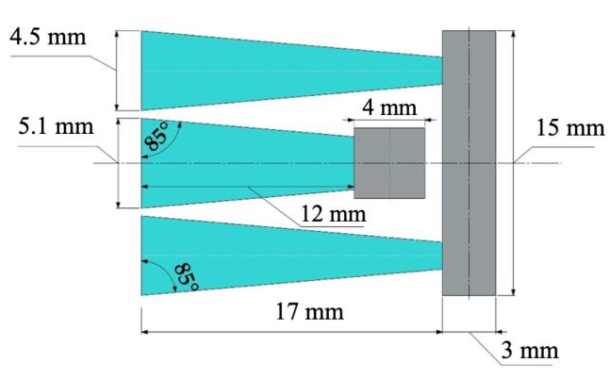
The dimensions of the beams that comprise the device are shown in Figure 2. The central beam has a base of 5.10 mm, a height of 12 mm, and a width of 3.8 mm at its opposite end. Meanwhile, the external beams have a base of 4.5 mm, a height of 17 mm, and a width of 1.8 mm at their opposite ends. These beams are proposed in a trapezoidal shape, which promotes a better distribution of the stresses present in the beam and improves energy harvesting [30,31,32,33,34]. This distributes the stresses along the beam, preventing them from accumulating at the base of each one [35], a phenomenon that occurs when the structure is based on a rectangular design. The literature indicates that the design directly affects the base excitation of the beam [36], resulting in a 30% increase compared to rectangular based designs [36].
In the literature, piezoelectric energy harvesting (EH) devices using silicon substrates have been reported, but these devices are limited by the fragility of the material, which increases the risk of fracture with large vibrations [37]. To overcome this issue, we designed a substrate using SS304 stainless steel, which is ductile, maintains its strength even with thicknesses in the order of microns, and can withstand the necessary temperatures during the manufacturing process. Additionally, a photosensitive resin seismic mass measuring 4x4x2 mm is implemented at the end of the central beam.
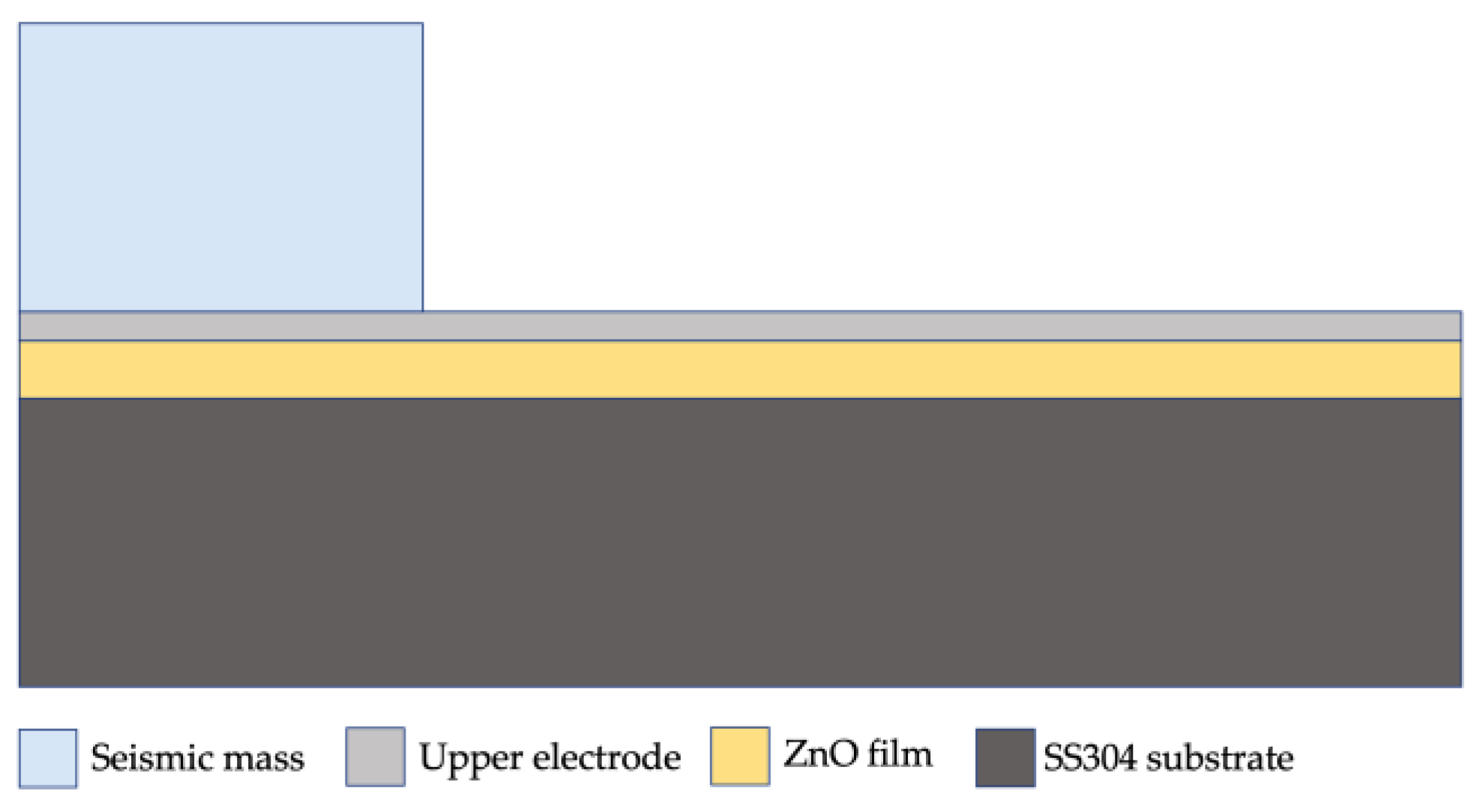
The remaining pair of beams are connected by a seismic mass of the same material, measuring 3x15x4 mm. Seismic masses are used in resonators as elements that can increase or decrease the resonant frequency of the device. The greater the seismic mass, the lower the resonant frequency [35]. As part of the design, the layers to be deposited on the substrate are considered, firstly, a multilayer ZnO film with a thickness of 1 micrometer, a top electrode, and finally, the two seismic masses mentioned above, as shown in Figure 3. In this device, the substrate also functions as the bottom electrode, which is necessary for energy extraction from the microgenerator.

2.2. Finite Element Model

To predict the behavior of the beams and determine their resonance frequency, finite element models (FEM) were developed using ANSYS® software based on the CAD design. The models considered the SS304 stainless steel substrate (50 µm thick), the piezoelectric film (1 µm thick), and the seismic masses. The upper electrode was neglected in these calculations due to its thinness, reducing the computation time and the number of elements required.
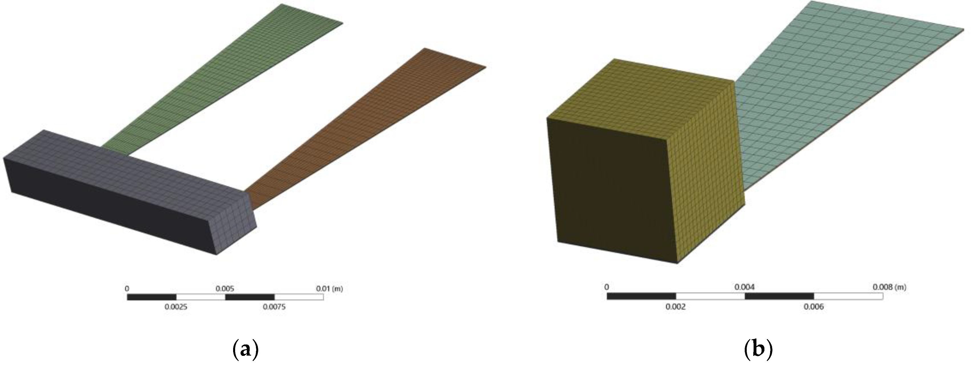
The beams were fixed at one end, and only the opposite end was allowed to move. Modal analysis was performed using FEM to obtain the first mode of vibration of the resonant structures. Each set of beams were simulated separately, with the outer set of beams using a mesh with 55,218 nodes and the central beam using a mesh with 55,579 nodes, creating a denser mesh and finer consistency in the area where the greatest stresses will occur due to the movement of the beams. as shown in Figure 4.
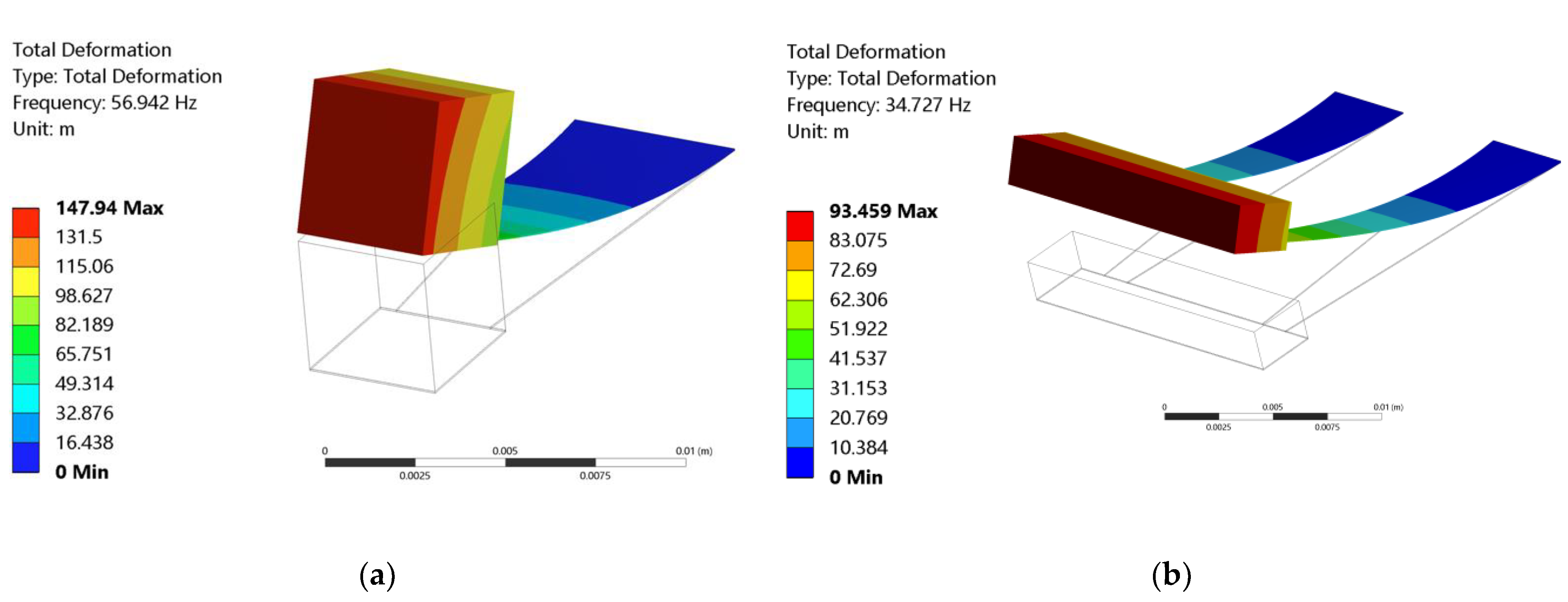
The first mode of vibration where the largest displacements are found was at a resonance frequency of 56,942 Hz for the central beam, while for the pair of external beams it occurs at 34,727 Hz. Figure 5 shows the results obtained using ANSYS® software of the deformation that exists in the beams at these frequencies.

2.3. Micromachining

To initiate the manufacturing process, the substrates were cleaned, as impurities due to their manufacturing process affect the adhesion of the films to be deposited on them. Sheets of SS304 steel measuring 1.5x1.5 cm were placed in a beaker submerged in an ultrasonic bath. After rinsing with distilled water, they were introduced into a second ultrasonic bath, placed in a beaker with distilled water only for 5 minutes at 60°C, and then dried with compressed air.
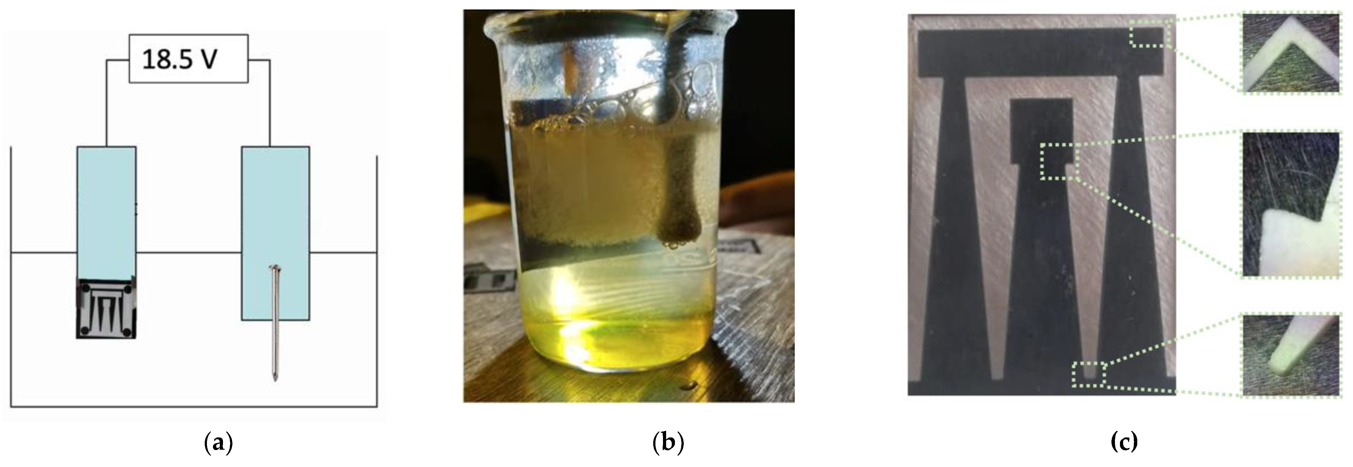
After the cleaning process, alignment-marked masks were created in a guard-ring position to convey the geometry of the PEH. The pattern was then printed using the pre-press technique to achieve higher resolution and image quality, facilitating the subsequent fabrication of PEH. A photosensitive polymer or dry film was applied to protect the areas of the stainless-steel substrate that were not intended to be etched. A mask with the desired geometry was then placed on the substrate, and the substrate was exposed to UV light for 2 minutes. This mask protected the areas that were not to be etched, and the substrate was developed using a mixture of 50 ml of distilled water and 0.5 grams of sodium carbonate. The etching process was carried out via electrolysis after applying a dry film to the substrate with a copied topology. To etch the substrate, a mixture of 100 ml water and 100 grams of sodium chloride was prepared and placed according to the configuration shown in Figure 6a. The voltage applied was 18.5 volts DC for 5 minutes, which resulted in the desired geometry (Figure 6b).
The micromachined substrate (Figure 6c) was inspected, particularly at the corners and joints, to qualitatively evaluate the etching, where appropriate definition was confirmed under an optical microscope. The same figure also demonstrates that the angles obtained by the beams after micromachining were suitably defined.
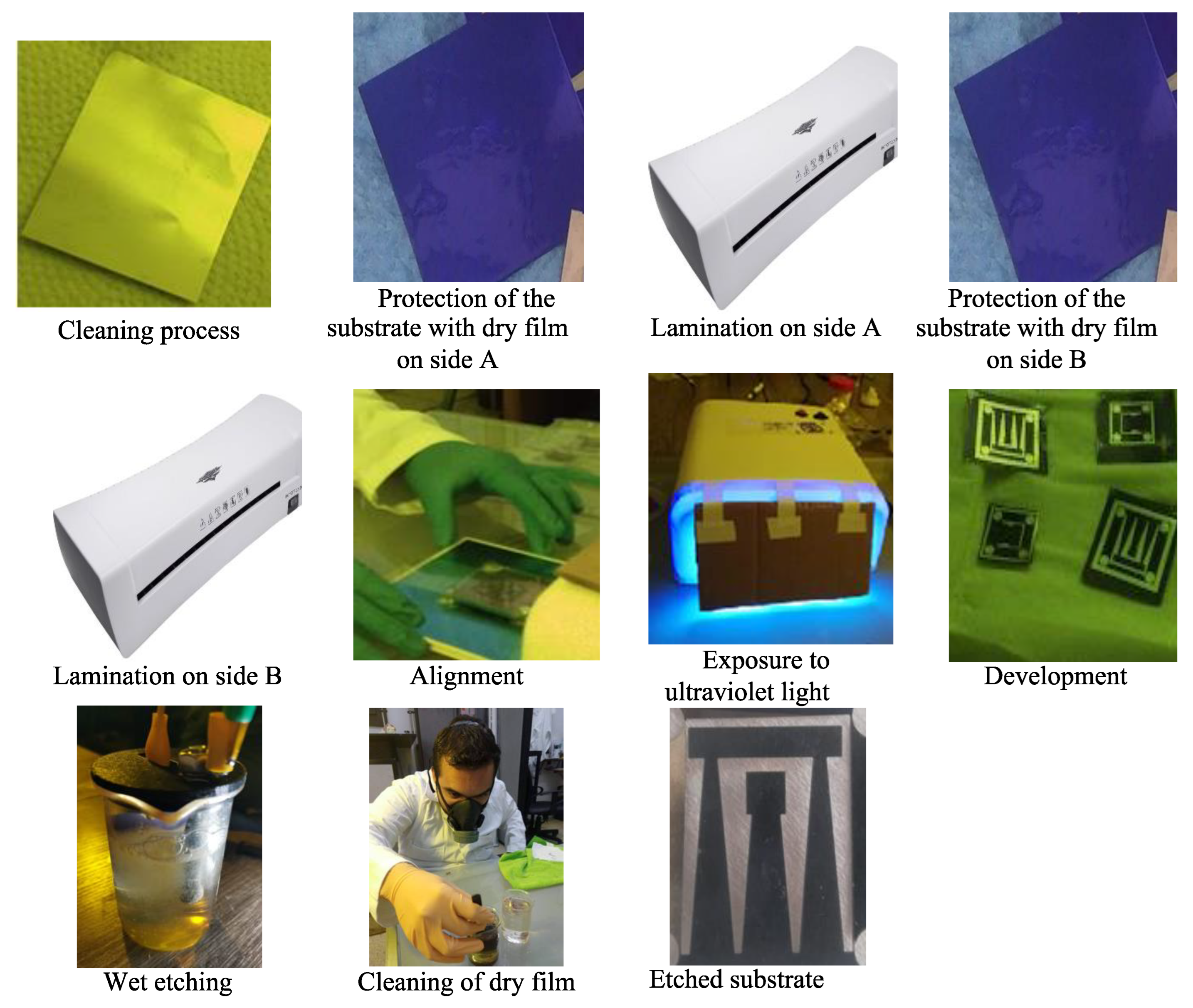
The micromachining methodology for the collector is shown in Figure 7 and is as follows:
  • Substrate protection with dry film: The substrate was protected with dry film, preventing the incorporation of clusters and bubbles on the surface.
  • Lamination: The substrate with dry film is laminated with a commercial laminator. This process is carried out on both sides of the substrate.
  • Alignment: The mask is aligned with the substrate previously protected with dry film.
  • UV light exposure: The mask is exposed to ultraviolet light for 3 seconds.
  • Development: In a solution of 50 ml distilled water and 0.5 grams of sodium carbonate, the substrate is developed, and after 30 seconds, excess dry film is removed.
  • Wet etching: a mixture of 100 ml water and 100 grams of sodium chloride was prepared, and a voltage of 18.5 V DC was applied for 5 minutes to remove the steel that does not belong to the PEH device structure.
  • Dry film cleaning: The etched substrate is cleaned with acetone.

2.4. Piezoelectric Film Synthesis and Deposition

The procedure employed for synthesizing the material for multilayer film deposition consisted of a combination of sol-gel chemistry, which involves hydrolysis and condensation reactions [38]. Zinc acetate dihydrate was utilized as a precursor, while monoethanolamine (MEA) was used as a catalyst and ethanol as the solvent, which proved to be more cost-effective and accessible for large-scale synthesis. The catalyst and solvent play a crucial role in the hydrolysis and condensation rates as well as the structure of the final product [39]
The process involved mixing 14 ml of ethanol and 1.55 mg of zinc acetate for 15 minutes at 80°C with continuous stirring in a stirring rack. Following this, 430 µl of monoethanolamine were added to the mixture, resulting in a transparent solution. The synthesis was carried out under ambient conditions, with a temperature of 25°C and a relative humidity of 70%.
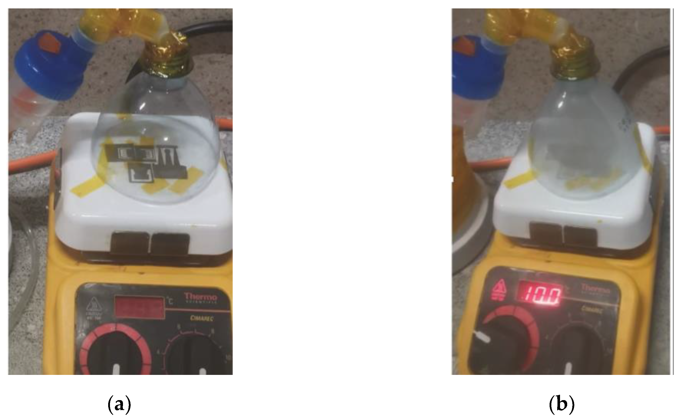
Following the synthesis process, a spray deposition technique was employed to deposit multilayer films. This technique was carried out while maintaining a constant pressure of 35 psi, an ambient temperature of 36°C, and a relative humidity of 70%. In order to maintain this pressure, a commercial-grade Trupper model COMP-50LT of 50 liters compressor was utilized. A commercial-grade nebulizer cup was attached to the compressor's outlet, and the solution containing the specified quantities of precursor, catalyst, and solvent employed in the sol-gel synthesis process was introduced into the nebulizer cup. The constant pressure provided by the compressor agitates the liquid contained in the nebulizer cup, converting it into a fine mist of vapors directed towards a preheated stirring grate at 100°C. The resulting film is deposited onto a previously micromachined stainless steel substrate. A chamber made from previously sterilized recycled materials was adapted to contain the aerosol. Once the chamber becomes saturated, the vapor droplets are deposited onto the substrate.
A multilayer deposition was carried out, where the precursor synthesis solution was used in each layer for a duration of 10 minutes at a deposition temperature of 100°C, resulting in a film with 10 layers deposited through the aforementioned process. After the completion of the multilayer film deposition, a post-thermal treatment was executed subsequent to rapid annealing. This procedure was implemented with the aim of transforming amorphous structures into crystalline ones by heating them at a temperature of 150°C for a duration of 2 minutes. The treatment facilitated the densification of the sol-gel while concurrently circumventing the condensation of agglomerated nanoparticles induced by the presence of reactants.
The mist deposition process starts when a fine mist was introduced into a chamber where it comes into contact with the surface to be coated, as shown in the following Figure 8. The mist droplets collide with the surface and adhere to it, forming a thin film.
Ultimately, substrate samples featuring 10-layer films each were prepared for thermal treatment in a muffle furnace at varying temperatures, facilitating the comparison of the effects on the films. The samples were annealed at 450°C, 500°C, and 550°C for a duration of 2 hours, with the treated samples being designated as Z450, Z500, and Z550, respectively.
In the final step of the device fabrication, seismic masses were produced using a mold designed on a CAD software and printed in a 3D commercial printer, incorporating transfer patterns for mold creation, which were subsequently saturated with a commercial photosensitive resin. The tailored seismic masses conformed to the collector's dimensions, achieving a seismic mass of 4x4x1 mm for the central beam and a 15x3x1 mm mass for the seismic mass situated at the junction of the outer beams. Upon introducing the photosensitive resin, it is subjected to UV light exposure for 5 minutes to induce hardening. This process ensures adhesion to the substrate, accommodating the displacements experienced during device excitation throughout electrical and mechanical characterizations. After the device fabrication, characterizations were performed on the ZnO films, and the electrical properties of the device were assessed by mounting it on an electromagnetic exciter connected to both a function generator and a DC source. The exciter was employed to induce vibrations at the resonance frequency of both beam sets, with the voltage generated by the collector being measured.

3. Results and discussions

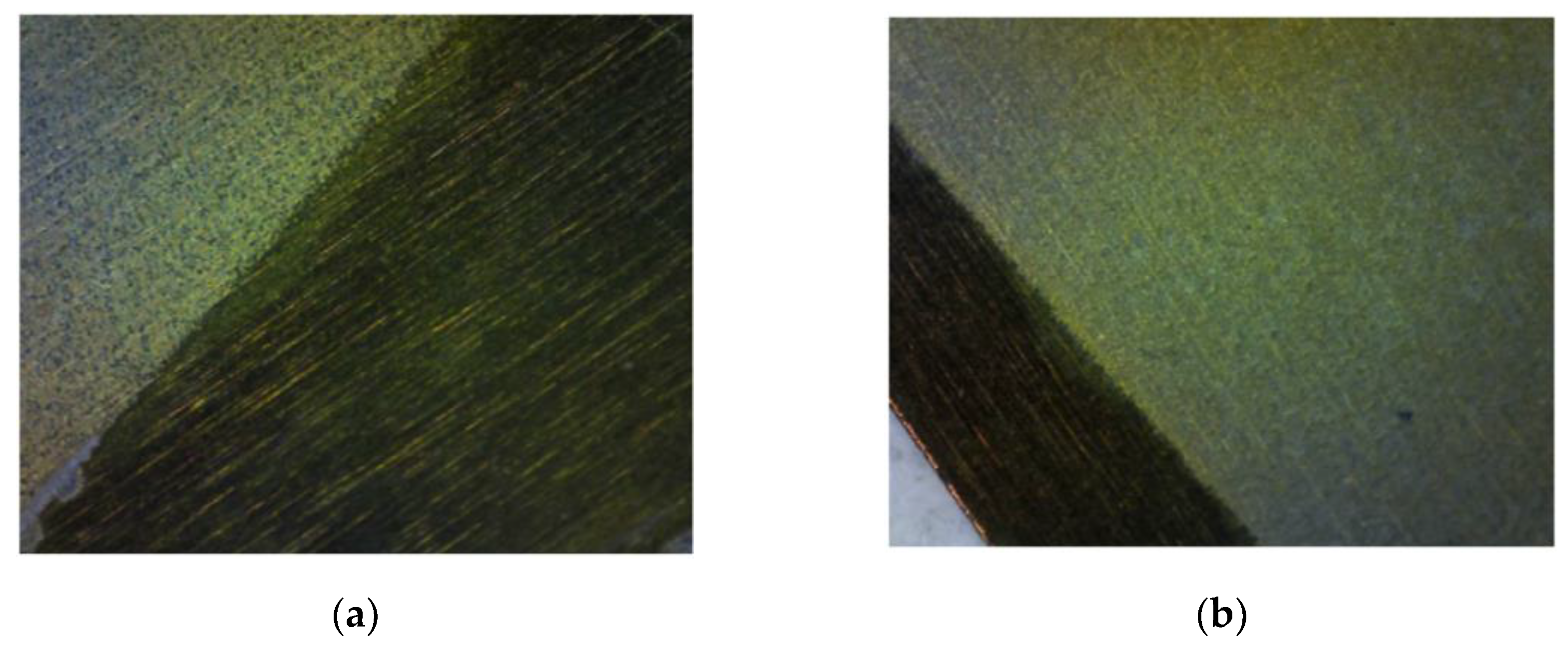
Following a thorough examination under an optical microscope, it was qualitatively discerned that the films depicted in Figure 9 demonstrated a remarkable degree of homogeneity, consistently enveloping the entire substrate area without manifesting any discernible cracks or crazing. This evidence suggests that the deposition process effectively yielded a film characterized by uniform thickness and density, devoid of conspicuous defects. The absence of cracks or crazing constitutes a critical attribute for films, as it signifies their inherent structural stability and diminished propensity to delaminate or fracture under stress. Furthermore, the uniform coverage of the substrate implies that the interfacial adhesion between the film and the substrate is robust, which is indispensable in averting potential film detachment.
To determine the thickness of the ZnO films, a Veeco Dektak 150 profilometer was used. The equipment performs a 3 mm scan over the surface using a microtip. The scan begins 1 mm before the step incorporated in the film and ends 2 mm on the film. The measurements were taken on substrates with ZnO multilayer films, obtaining an average thickness of 1 μm.

3.1. Optical analysis of ZnO films

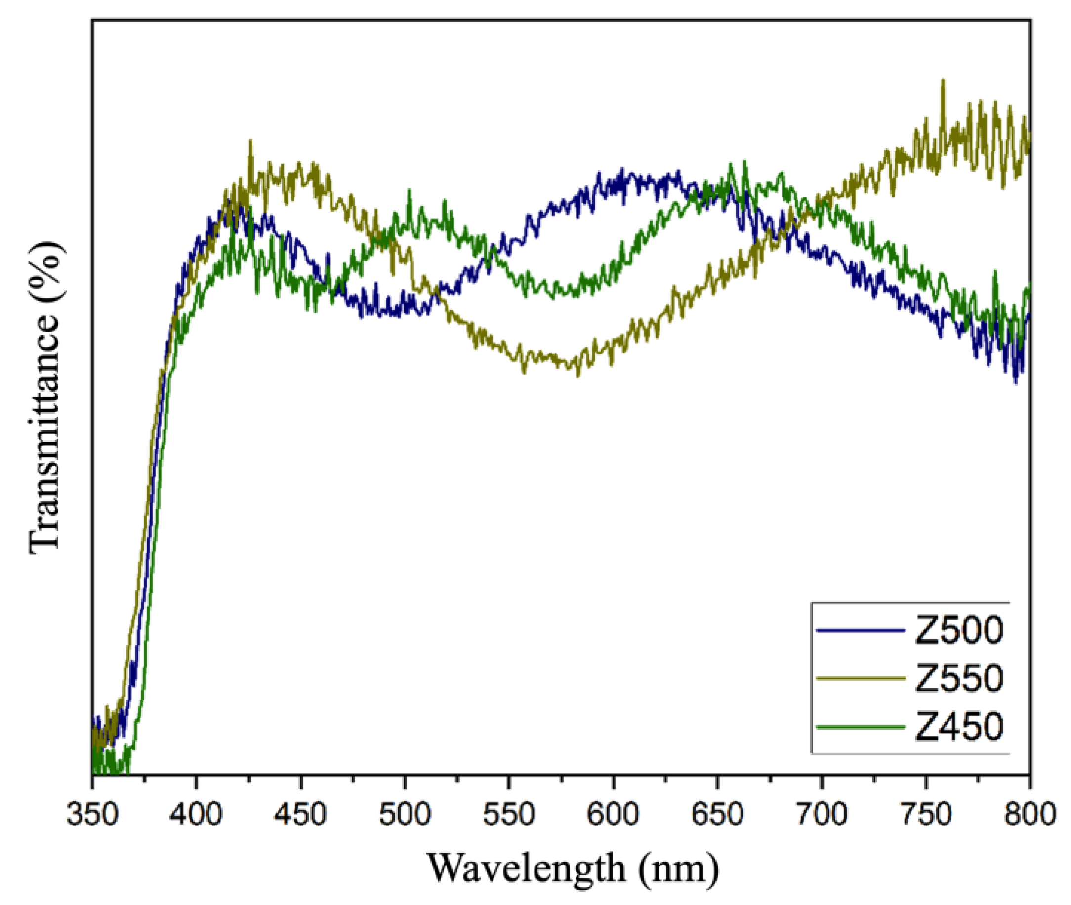
To verify the presence of ZnO on the substrates, reflectance percentage characterizations were performed using a Thermo Scientific EVOLUTION 600 UV-Vis spectrophotometer. The transmittance percentage results (Figure 10) reveal an initial peak commencing at 370 nm, confirming the presence of ZnO since it absorbs light at a wavelength of approximately 375 nm.
The graph also exhibits sinusoidal oscillations in all measurements following the initial peak, indicative of film homogeneity [39]. Furthermore, a noticeable shift to the right is observed in the measurements of thermally treated films, suggesting an increased grain size in the film [40]. Consequently, we can assert that the obtained film behaves as anticipated by absorbing light at a specific wavelength, in line with existing literature on ZnO films.

3.2. Scanning electron microscopy

The morphological characterization of the piezoelectric film was using a JEOL JSM-7600F scanning electron microscope with a magnification of 10,000x, 20,000x and 30,000x respectively. Upon analysis of the film and its composition, a rough surface was observed, indicating strong adhesion of the piezoelectric material to the substrate. Furthermore, the uniformly rough surface observed suggests a homogeneous and consistent piezoelectric behavior throughout the device.
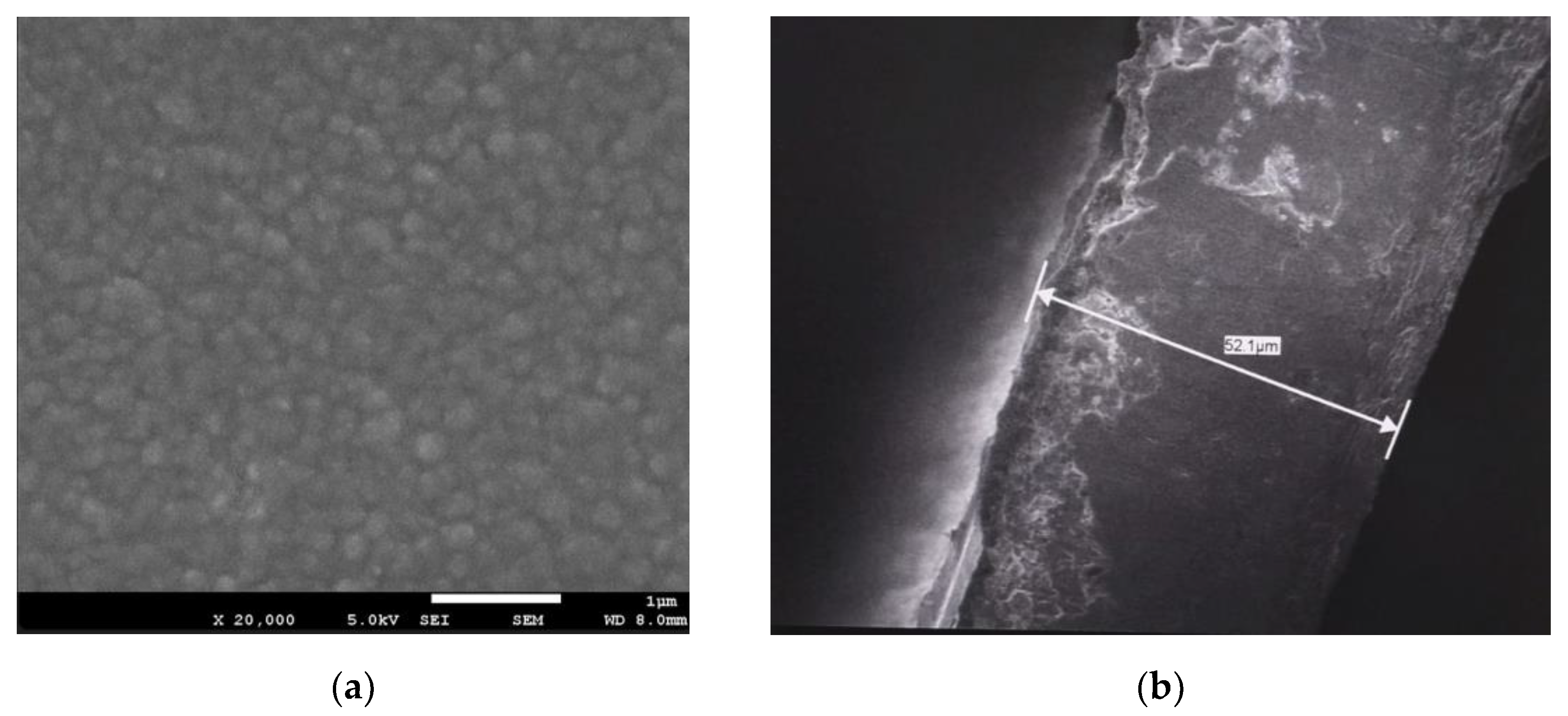
Nanostructured flakes have been observed in micrographs of ZnO, which not only facilitate the piezoelectric phenomenon, but also provide bulk material with a high level of mechanical strength [41]. This mechanical strength prevents the material from fracturing or cracking when used in vibrational devices, as illustrated in Figure 11. Moreover, an analysis of scanning electron microscope (SEM) images confirmed the presence of 250-nanometer diameter nanospheres, thereby confirming the successful production of nanostructured films.
The production of a ZnO nanostructured film represents a significant advantage in energy harvester manufacturing. The unique physical and chemical properties of ZnO nanostructures are capable of significantly enhancing energy collection efficiency [42]. Particularly noteworthy is the discovery of 250-nanometer ZnO nanospheres in this study, which highlights the successful production of nanostructures using cost-effective synthesis and deposition techniques. This finding represents an important contribution, demonstrating the potential of practical and economical equipment in achieving the ideal form of nanostructures.
These ZnO nanospheres exhibit a high degree of porosity, resulting in a large surface area and excellent electrical conductivity, thereby increasing their energy capture capability [43]. Moreover, their uniform size and shape allow them to effectively bind together in a nanostructured film, further enhancing their efficiency in energy collection [44]. It was also possible to observe the high quality of the ZnO film, exhibiting homogeneity and being free of visible defects on the surface.
Furthermore, the thickness of the substrate was measured, resulting in 52.1 mm, as shown in Figure 12. This measurement corresponds to the model used for the simulations of the energy harvesting device, providing important validation of the simulation results. These significant findings provide valuable insights for the development of future piezoelectric devices for harvesting energy.

3.3. X-ray Diffraction (XRD)

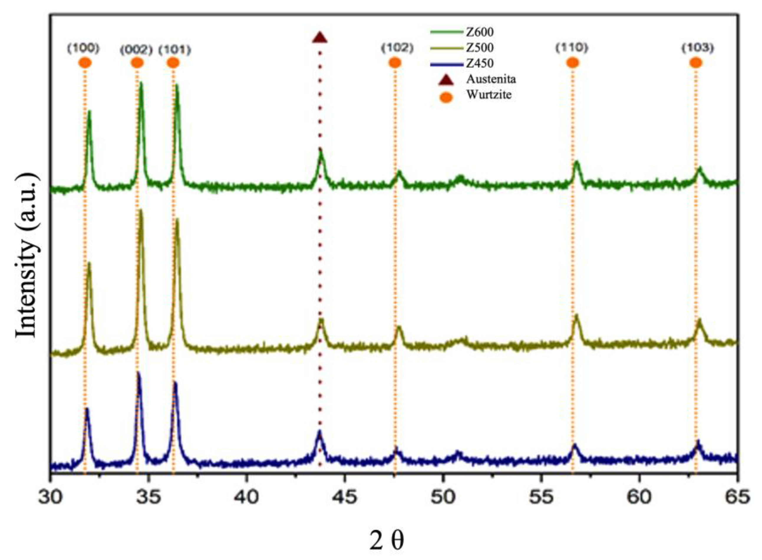
In order to confirm the presence of zinc oxide and its growth phase in the nanostructured ZnO films, X-ray diffraction was performed to obtain the materials' crystal structure. The diffraction pattern of the ZnO samples revealed the presence of wurtzite phase ZnO with preferential growth on the (101) plane, as Figure 13 shows). Additionally, well-defined peaks at 35°, which are characteristic of ZnO in the wurtzite crystal structure [45], were observed.
The absence of other materials in the diffraction pattern suggests that the synthesis and deposition processes of the piezoelectric films were successful and free of impurities. These findings provide valuable insights into the crystal structure and growth phase of ZnO nanostructured films, thus confirming their potential suitability for use in piezoelectric energy harvesting applications.
Furthermore, all samples demonstrated high crystallinity, indicating the quality of the crystal structure and the uniformity of crystal orientation [45]. The annealing process applied to the films was found to be within the temperature range that promotes grain growth, which is closely related to the piezoelectric response of the material [46]. Additionally, the grain size of the films plays a crucial role in light transmission, which is essential for the efficiency of the piezoelectric energy harvester.
However, it was observed that films subjected to a thermal treatment at 550°C over time showed detachment from the substrate, which is likely due to the mechanical stress and deformation induced by the high temperature [47]. Therefore, it is recommended that a lower annealing temperature be used to produce suitable films for the process.
The crystal size of ZnO was theoretically calculated using equation (1) based on the (002) peak.
L = k λ β cos θ
The method employed for calculating the size of nano crystallites (L) using XRD radiation involves the measurement of the full width at half maximum (β) of the peaks located at any 2θ angle in the pattern, given a wavelength of λ (in nm), expressed in radians. The results show a correlation between the annealing temperature and the crystallite size in ZnO samples. It was found that as the annealing temperature increases, the crystallite size in the samples also increases. Specifically, sample Z450 exhibited a crystallite size of 18.22 nm, while sample Z500 and Z550 displayed sizes of 29.10 nm and 29.36 nm, respectively. This increase in crystallite size can be attributed to the higher thermal energy present at higher annealing temperatures, which allows atoms to move more freely and promotes crystal growth [48].
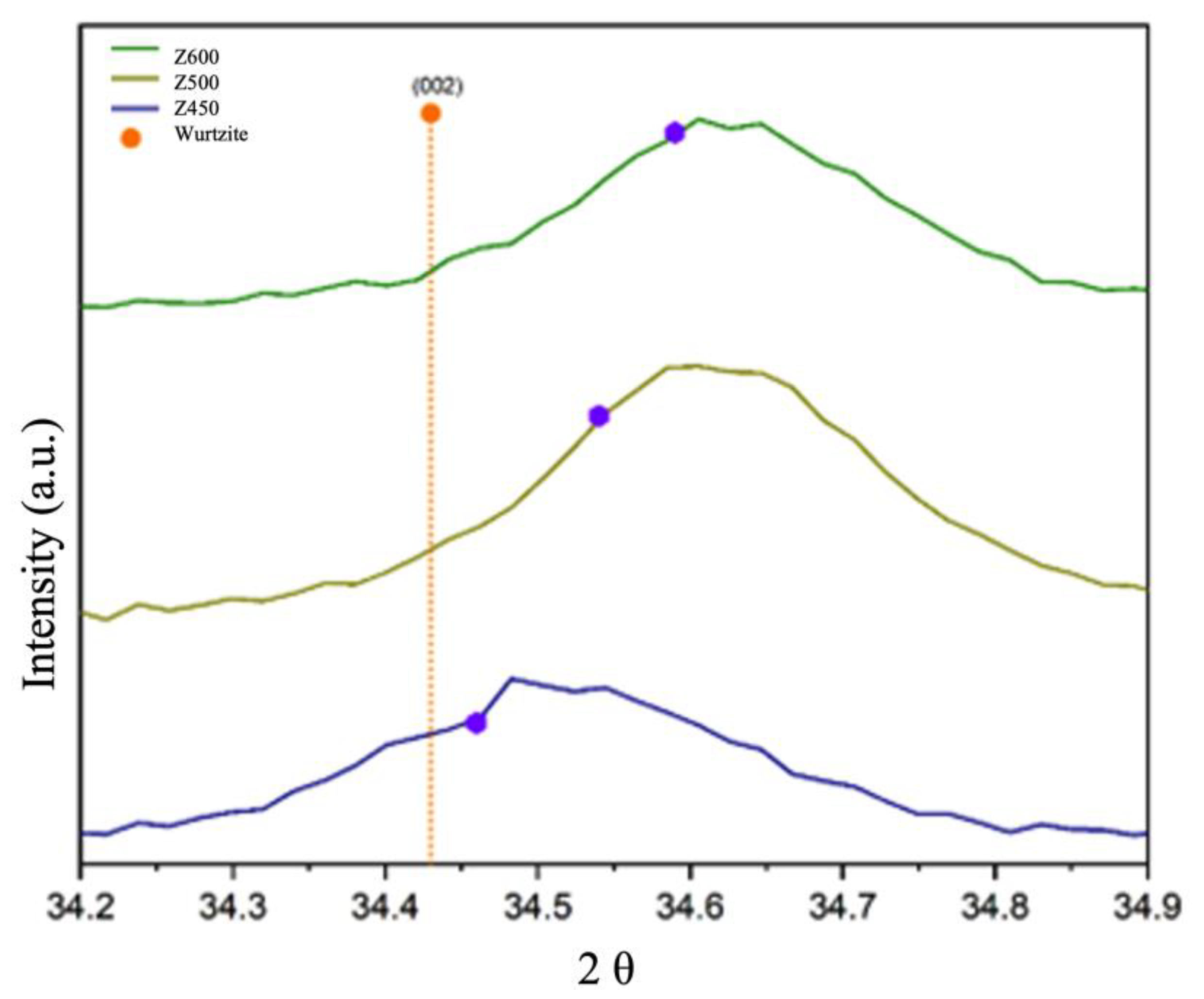
It is worth noting that the size of the crystallite can significantly affect the piezoelectric and optical properties of the material, thus having a significant impact on the efficiency of piezoelectric energy harvesters [43]. As shown in Figure 14, the diffractogram of the ZnO films in the (002) crystal plane exhibited a minor shift towards compression with increasing temperature. This shift was analyzed using the Stoney equation [49], revealing a tensile shift for the Z450, Z500, and Z550 films at 2θ of 34.46, 34.54, and 34.59, respectively. These findings highlight the importance of carefully controlling annealing temperature to optimize the crystallite size and ensure efficient performance of ZnO-based piezoelectric energy harvesters. Figure 14 shows the X-ray diffraction patterns of ZnO films on the (002) crystal plane. As the temperature increases, a small compression shift is observed, which was analyzed using the Stoney equation.
The compressive stress of the ZnO films was calculated and found to be -2.81 GPa for Z450, -2.07 GPa for Z500, and -1.85 GPa for Z550. Based on its higher intensity in the (002) crystallographic plane, the Z450 film was selected for electrical characterization to determine the power output of the piezoelectric generator.

3.4. Electrical characterization

A custom vibration system was designed and constructed to control a vibration source for research on vibration energy harvesting devices. The system employs a modified subwoofer from a commercial DVD home theater audio system as the vibration source to meet research requirements.
Figure 15a illustrates the schematic for the custom vibration system, which incorporates a commercial audio loudspeaker with a designated area for test samples mounted on the loudspeaker cone. A laboratory function generator produces the excitation signal, and a unity gain power amplifier supplies the current necessary to drive the subwoofer's low impedance.
A broadband vibrometer serves as the reference accelerometer, while an oscilloscope measures and displays the energy harvesting output signal. The selection of an 8-inch subwoofer was based on its size, robust construction, and compatibility with the intended modifications. A 3D-printed plastic plate was designed and affixed to the speaker cone using adhesive glue, creating a flat surface at the cone's center. Additionally, a unique part was printed for the energy harvester device pickup, elevating the test surface above the embedded cone area and mitigating the strong magnetic influence from the loudspeaker. The subwoofer is housed in a custom acrylic enclosure.
Figure 15b presents a photograph of the complete vibration system featuring the micromachined substrate without deposited films and offers a close-up view of the fabricated device area with piezoelectric film and seismic masses, displaying intricate construction details. The vibration amplitude of the exciter is assessed using a calibrated reference vibrometer, while the size and frequency of oscillations are regulated by a function generator configured to produce a zero-offset sine wave output. Overall, the custom vibration system delivers a controllable vibration source that is ideally suited for research on vibration energy harvesting devices.
To provide the necessary current gain for the low impedance of the subwoofer, a power amplifier was required. Specifically, the audio mono TPA3118 60w Arduino voltage amplifier model was used. This amplifier was selected due to its ability to provide the required gain and its compatibility with the experimental setup. The amplifier was mounted within the setup, as shown in Figure 15, and was used to amplify the voltage signal in order to drive the subwoofer. The use of this amplifier allowed for precise control over the output signal and ensured that the subwoofer received the necessary amount of power to produce the desired sound.
The experiment was conducted with a total of 10 repetitions, which were deemed sufficient to obtain reliable and meaningful results [50]. The collectors were placed within a 3D printed mold to maintain stability during the agitation process. The excitation frequency was varied from 0 to 60 Hz to identify the resonance frequency of both sets of beams experimentally, as shown in Figure 16. The experiment revealed the existence of a piezoelectric effect, as the vibrations were observed to influence the generator.
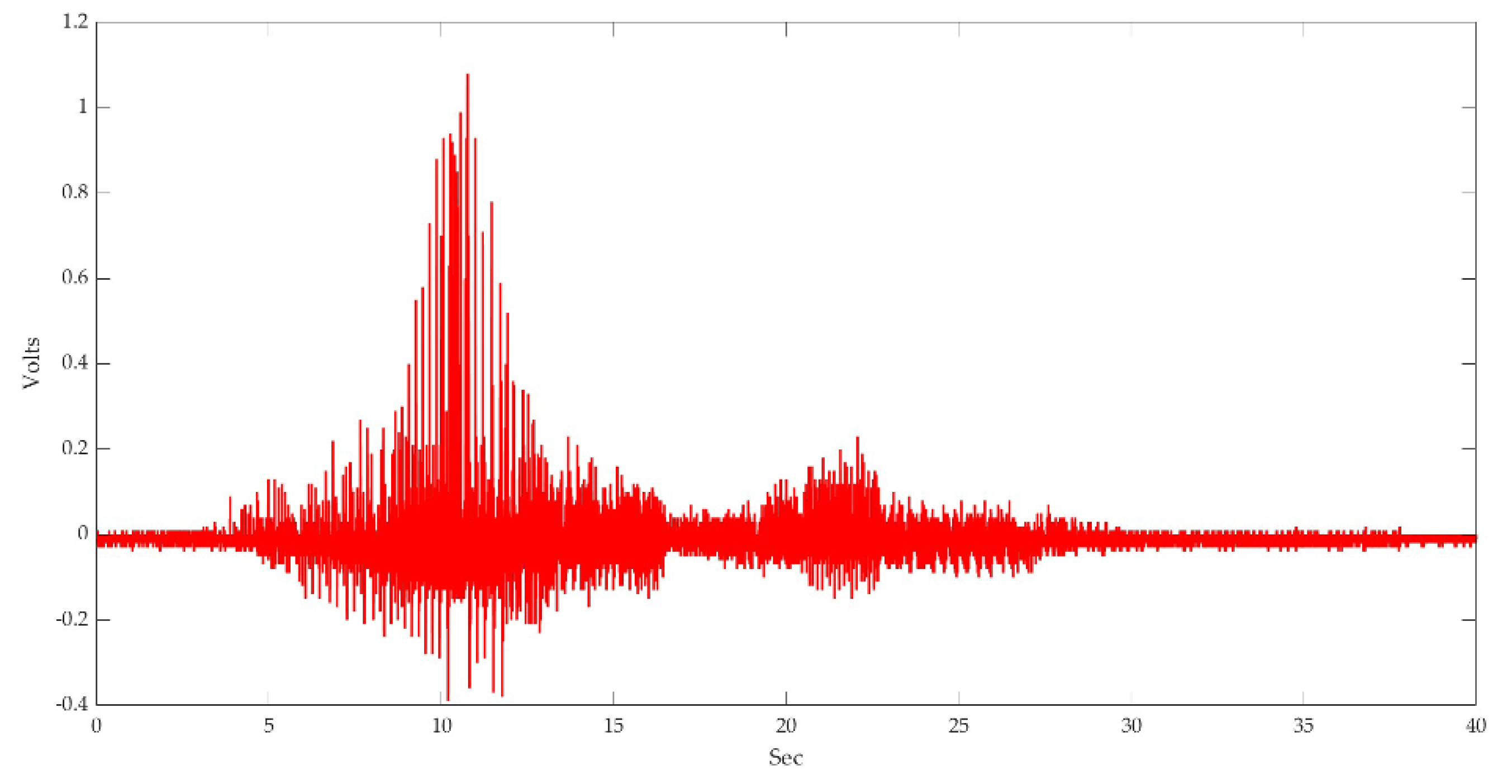
Data collected from the experiment were processed, and a standard deviation of 0.084 was observed in the external beams, while the central beam had a standard deviation of 0.097. These values indicate that the data are relatively close to the mean and that there is little variation in the dataset [51]. Overall, the experimental setup and results demonstrate the effectiveness of the electromagnetic shaker and provide important insights into the behavior of the fabricated collectors. During the measurement, the average maximum voltage observed for the external beams was 1.08 V, while for the central beam it was 180 mV. As depicted in Figure 16, an increase in voltage occurred as the resonance frequency was approached, which was experimentally evaluated to be 35 Hz and 58.5 Hz for each set of beams, respectively.
This represents a 0.78% difference from the FEM simulation results for the external beams. In the case of the central beam, there was a 2.7% difference when comparing the experimental displacement with the ANSYS simulation. These results are within the 5% difference range that is commonly accepted in the literature when comparing simulated and experimental data.
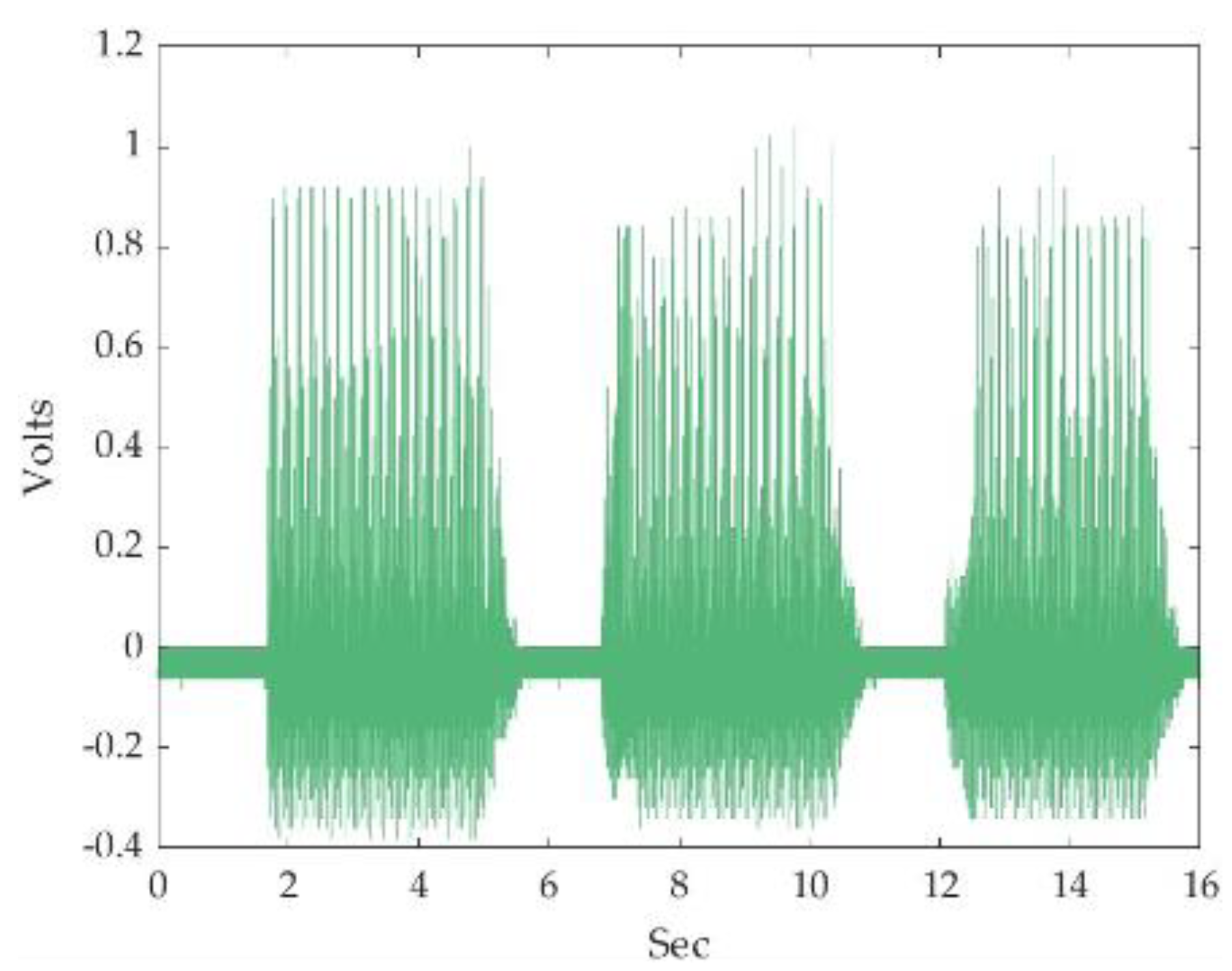
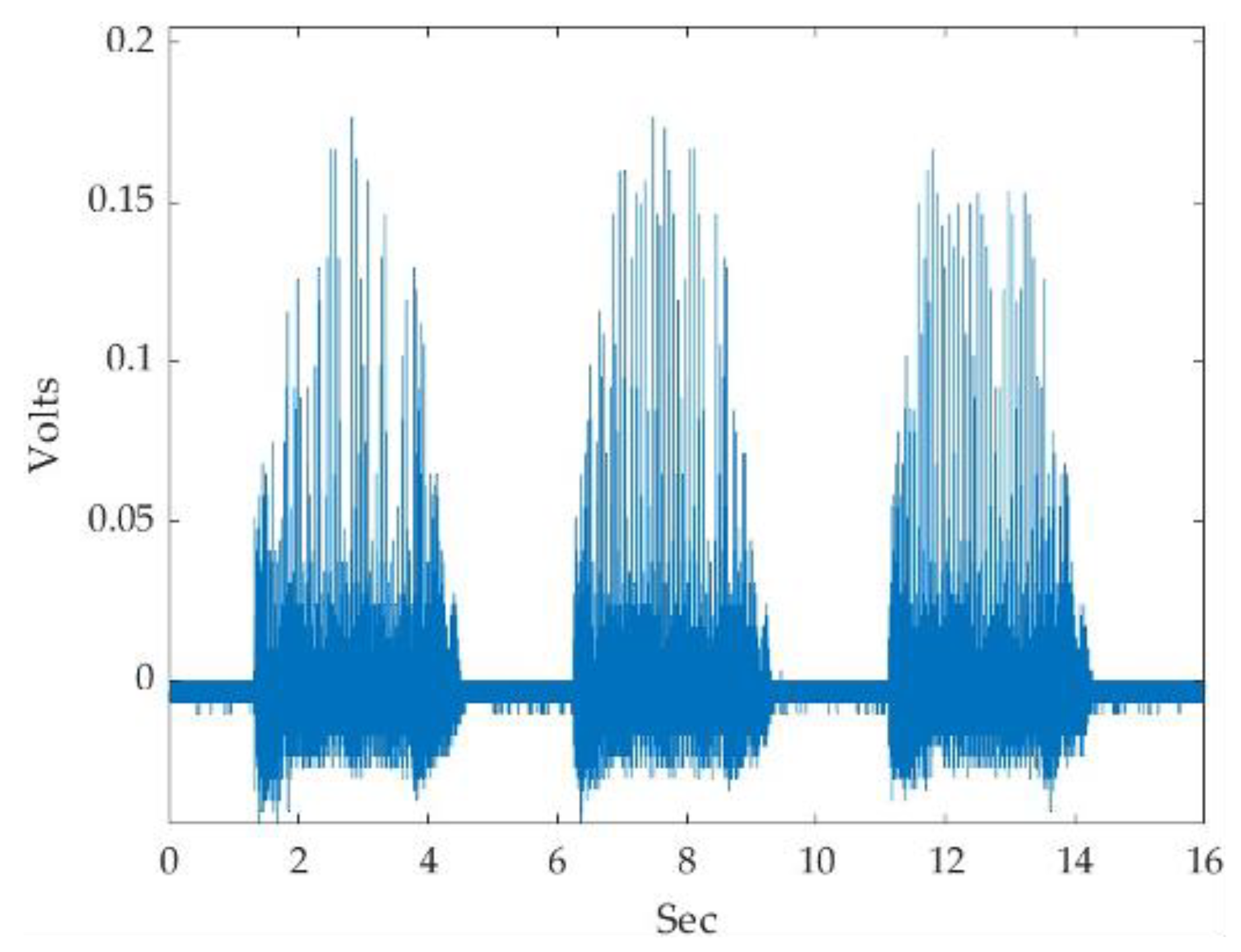
Furthermore, to observe the piezoelectric response, the shaker's excitation was randomly stopped, and the beams' response was measured, obtaining the results shown in Figure 17 for the outer beams and Figure 18 for the central beam. The results showed that the external beams had a significant piezoelectric response, reaching an average voltage of 1.08 volts during excitation.
When the mechanical vibrations provided by the shaker were inhibited, the voltage values approached zero. Both Figure 17 and Figure 18 display the voltage values obtained, and it is evident that a significant voltage drop occurs when the excitation is interrupted.
The results suggest that the external beams have a higher piezoelectric response than the internal beam, indicating that they may be suitable for certain applications that require a strong piezoelectric response.
As stated above, the results demonstrated that the piezoelectric film operated correctly, as there was no energy collection when the device was left without movement. The central beam generated between 155 and 180 mV when oscillating at a frequency of 58.5 Hz, as illustrated in Figure 18. The measurements taken suggest that the piezoelectric film on the central beam is effective at generating energy when the beam vibrates at its resonance frequency. The results are promising and indicate that the device may have practical applications in generating energy from mechanical vibrations.
On the other hand, to demonstrate the measurements taken to calculate the power generated by an energy harvesting device, the experiment involved the use of resistors of varying values ranging from 49.5 kΩ to 464 kΩ, while the devices were kept at their resonance frequency at different times. The resulting data obtained from these measurements have been presented in Table 1.
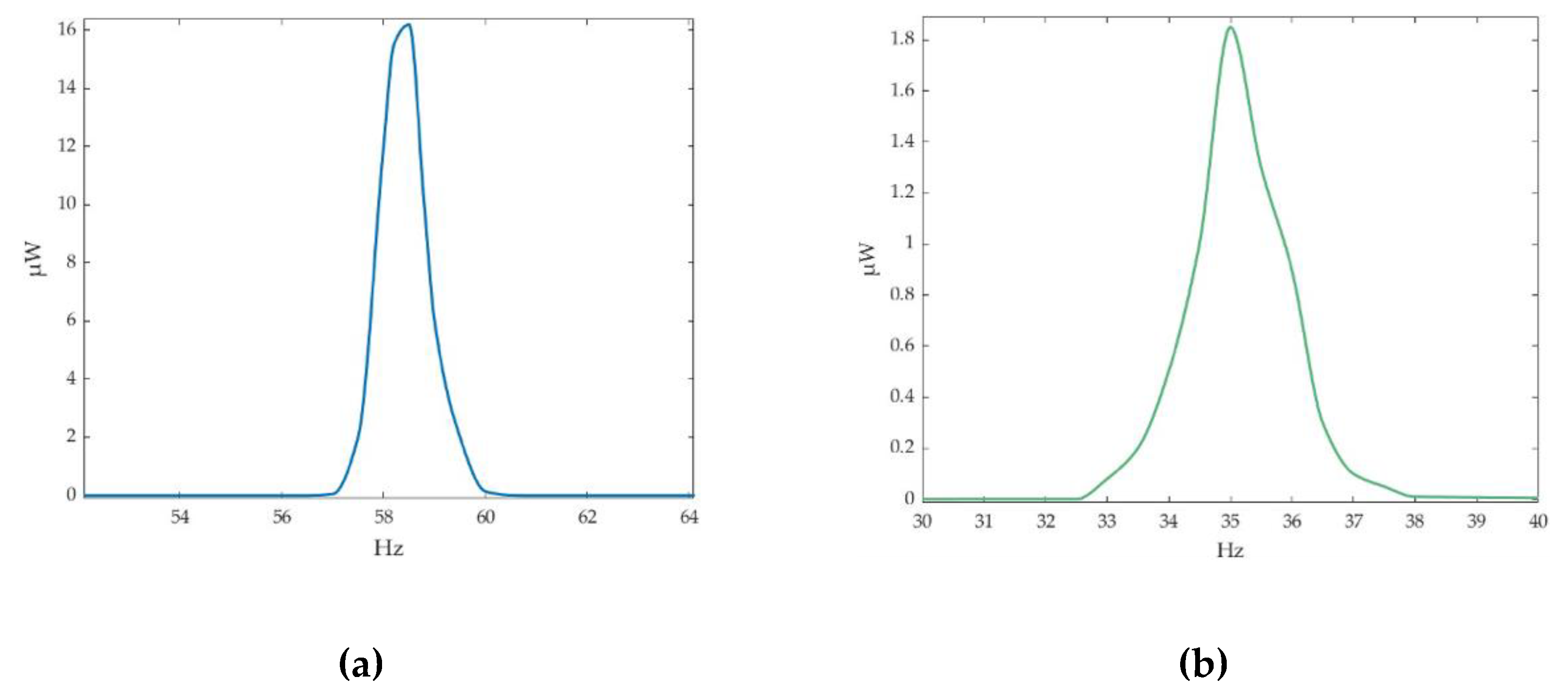
It is worth noting that the devices were maintained at their resonance frequency throughout the mentioned experiment. This was likely done to ensure that the device was operating at its maximum efficiency, which would provide more accurate results. The central beam generated a voltage of 80 mV and recorded an average maximum power output of 16.2 nW when a resistance of 100 kΩ was used. In contrast, the outer beams produced a maximum voltage of 860 mV and a maximum average power output of 1.84 µW when a resistance of 200 kΩ was used. The behavior of power output for the central beam is shown in Figure 17a, while the same behavior for the outer beams is presented in Figure 17b.
The voltage measurements obtained from the central and outer beams suggest that the outer beams are more effective at generating voltage than the central beam. However, the central beam recorded a higher power output at the given resistance level. It is important to highlight that the maximum power output was achieved when the beams were vibrating at their resonance frequency.
This suggests that the device operates most efficiently at its resonant frequency and could be optimized for performance by tuning it to this frequency. Additionally, the graphs provided in Figure 19a,b show how power output varies with changing resistance values, providing a visual representation of the experiment's findings.
In light of the gathered results from various research studies on energy harvesting by piezoelectric systems and in comparison, with the findings of this research, which employed piezoelectric materials such as Polyvinylidene Fluoride (PVDF) or Lead Zirconate Titanate (PZT), Table 2 warrants significant attention.
One notable aspect of this energy collector's production is the omission of PZT, which eliminates the release of lead into the environment during the deposition process of the piezoelectric film. This significant change significantly diminishes the environmental impact that typically arises from the production of such devices.
Moreover, this study employs piezoelectric film thicknesses that are 50% lower than those used by other authors who achieve greater power outputs, such as those reported in references [53] and [52]. It is also noteworthy that up to 200% less piezoelectric material was used during the design and fabrication of the energy harvester in this study, leading to considerable savings in chemical use and creating a more environmentally conscious process in line with the objectives of the 2030 Agenda.
In addition, the set of external beams has been found to generate a higher amount of electrical power than other recent works in the field of energy harvesting, including those carried out by the University of Applied Sciences Zittau Görlitz in Germany [59] and the Department of Electrical and Electronic Engineering at Imperial College London in England [56].
Further analysis reveals that the central beam generates 50% more power than reported in 2022 [58] and is capable of producing up to three times more voltage when subjected to vibrations at its resonance frequency. These findings have significant implications for manufacturing costs and potential consumer base and provide an opportunity for greater energy harvesting in the coming decade.

4. Conclusions

This study describes the design, modeling, and fabrication of a piezoelectric-based energy harvester. The harvester's geometry was designed using CAD software, which included a central beam and two outer beams with specific dimensions to optimize energy generation. The harvester was fabricated by using an AISI304 steel substrate as the bottom electrode, a nanostructured ZnO piezoelectric film, and a seismic mass of resin.
Finite element models were employed to simulate the harvester's behavior and determine the first resonant frequencies of both the central and outer beams. The maximum displacement of the device was calculated using FEM to ensure that the induced mechanical vibrations did not exceed the material's stress limits. Comparison of the FEM model with experimental results revealed differences of 0.78% and 2.7% for the central and outer beams, respectively. It can be observed that the similarity between the computational model and the experimental values obtained provides confidence in the results obtained during the simulation. Therefore, it can be considered that the simulation is appropriate and that the results obtained are accurate.
In that same context, a high-quality, uniform, and dense ZnO film was deposited using a sol-gel method, offering advantages such as low cost and simplicity in the fabrication process. For instance, this procedure exhibited behavior like that reported in the literature. Also, it was compared with the latest developments in energy-harvesting materials, but Plumb (Pb) was not used in this procedure in accordance with the objectives of the 2030 agenda for sustainable development, which aims to prevent the release of pollutants from industrial, shipping, and agricultural activities.
The annealing process caused a reduction in the thickness of the resulting film, which can be attributed to the evaporation of the solvent. This resulted in the formation of a hexagonal symmetry related to the wurtzite structure, as confirmed by XRD analysis. Moreover, the use of a nanostructured ZnO film in the harvester promotes adhesion and increases the film's surface area, leading to greater energy collection efficiency. The results obtained in this study suggest that the film can be applied in various devices and applications.
Measurements were conducted to determine the power output of an energy harvesting device using varying resistance values ranging from 45.5 kΩ to 464 kΩ, while ensuring the device was maintained at its resonant frequency during each test. The central beam produced a voltage of 80 mV, while the outer beams generated a maximum voltage of 860 mV, resulting in a maximum power output for the device. These results demonstrate that the harvester is suitable for low-power applications and can serve as an efficient and economical alternative for powering such devices, taking into account the environment and the exponential use of this technology in the coming years.

Author Contributions

Conceptualization, L.A.U.-G. and E.A.E.-H.; methodology, A.L.H.-M. and F.L.-H. ; software, E.A.E.-H. and A.L.H.-M; validation, F.L.-H. and E.J.A.-S.; formal analysis, L.A.U.-G. and R.F.-L.; investigation, E.J.A.-S.; resources, F.L.-H. and A.L.H.-M.; writing—original draft preparation, L.A.U.-G. and E.A.E.-H.; writing—review and editing, R.F.-L. and E.J.A.-S.; visualization, L.A.U.-G. and E.A.E.-H.; supervision, A.L.H.-M.; project administration, A.L.H.-M. and F.L.-H.; funding acquisition, A.L.H.-M. All authors have read and agreed to the published version of the manuscript.

Funding

This work was supported by CONACYT with scholarship number 473284.

Institutional Review Board Statement

Not applicable.

Informed Consent Statement

Not applicable.

Data Availability Statement

Not applicable.

Acknowledgments

Luis A. Uscanga-González wishes to express his sincerest appreciation to the Doctoral Program on Engineering at Universidad Veracruzana for the outstanding academic training he received during his doctoral studies. Likewise, he extends his gratitude to the Micro and Nanotechnology Center (MICRONA) at Universidad Veracruzana for the training received at this outstanding research center. Lastly, he wishes to extend his heartfelt gratitude for the scholarship granted by the National Council of Science and Technology (CONACYT) under scholarship number 473284.

Conflicts of Interest

The authors declare no conflict of interest.

References

  1. Noh, C.; Shin, M.; Kwon, Y. A strategy for lowering cross-contamination of aqueous redox flow batteries using metal-ligand complexes as redox couple. J. Power Sources 2022, 520, 230810. [Google Scholar] [CrossRef]
  2. Mumtaz, S.; Jiang, C.; Tolli, A.; Al-Dulaimi, A.; Butt, M.M.; Asif, H.M.; Ashraf, M.I. Guest Editorial: 6G: The Paradigm for Future Wireless Communications. IEEE Wirel. Commun. 2022, 29, 14–15. [Google Scholar] [CrossRef]
  3. Attaran, M. The impact of 5G on the evolution of intelligent automation and industry digitization. J. Ambient Intell. Humaniz. Comput. 2021. [Google Scholar] [CrossRef] [PubMed]
  4. Fazea, Y.; Mohammed, F.; Al-Nahari, A. A Review on 5G Technology in IoT-Application Based on Light Fidelity (Li-Fi) Indoor Communication. In; 2022; pp. 371–384.
  5. Wu, Y.; Li, Y.; Zou, Y.; Rao, W.; Gai, Y.; Xue, J.; Wu, L.; Qu, X.; Liu, Y.; Xu, G.; et al. A multi-mode triboelectric nanogenerator for energy harvesting and biomedical monitoring. Nano Energy 2022, 92, 106715. [Google Scholar] [CrossRef]
  6. He, T.; Lee, C. Evolving Flexible Sensors, Wearable and Implantable Technologies Towards BodyNET for Advanced Healthcare and Reinforced Life Quality. IEEE Open J. Circuits Syst. 2021, 2, 702–720. [Google Scholar] [CrossRef]
  7. Miraz, M.H.; Ali, M.; Excell, P.S.; Picking, R. A review on Internet of Things (IoT), Internet of Everything (IoE) and Internet of Nano Things (IoNT). In Proceedings of the 2015 Internet Technologies and Applications (ITA); IEEE, 2015; Vol. 113; pp. 219–224. [Google Scholar]
  8. Tan, Y.; Dong, Y.; Wang, X. Review of MEMS electromagnetic vibration energy harvester. J. Microelectromechanical Syst. 2017, 26, 1–16. [Google Scholar] [CrossRef]
  9. Yan, J.; Liao, X.; Yan, D.; Chen, Y. Review of Micro Thermoelectric Generator. J. Microelectromechanical Syst. 2018, 27, 1–18. [Google Scholar] [CrossRef]
  10. Chen, T.; Shi, Q.; Li, K.; Yang, Z.; Liu, H.; Sun, L.; Dziuban, J.; Lee, C. Investigation of Position Sensing and Energy Harvesting of a Flexible Triboelectric Touch Pad. Nanomaterials 2018, 8, 613. [Google Scholar] [CrossRef]
  11. Liu, L.; Guo, X.; Liu, W.; Lee, C. Recent Progress in the Energy Harvesting Technology—From Self-Powered Sensors to Self-Sustained IoT, and New Applications. Nanomaterials 2021, 11, 2975. [Google Scholar] [CrossRef]
  12. Wang, T.; Zhu, Z.W. A new type of piezoelectric self-excited vibration energy harvester for micro-actuator’s energy storage. J. Energy Storage 2022, 46, 103519. [Google Scholar] [CrossRef]
  13. Prajwal, K.T.; Manickavasagam, K.; Suresh, R. A review on vibration energy harvesting technologies: analysis and technologies. Eur. Phys. J. Spec. Top. 2022 2318 2022, 231, 1359–1371. [Google Scholar] [CrossRef]
  14. Pourashraf, T.; Bonello, P.; Truong, J. Analytical and Experimental Investigation of a Curved Piezoelectric Energy Harvester. Sensors 2022, 22, 2207. [Google Scholar] [CrossRef]
  15. Abouzarkhanifard, A.; Chimeh, H.E.; Janaideh, M. Al; Zhang, L. FEM-Inclusive Transfer Learning for Bistable Piezoelectric MEMS Energy Harvester Design. IEEE Sens. J. 2023, 23, 3521–3531. [Google Scholar] [CrossRef]
  16. Zhu, X.; Xiao, J.; Mao, Q.; Zhang, Z.; You, Z.; Tang, L.; Zhong, Q. A promising regeneration of waste carbon residue from spent Lithium-ion batteries via low-temperature fluorination roasting and water leaching. Chem. Eng. J. 2022, 430, 132703. [Google Scholar] [CrossRef]
  17. He, Z.; Li, W.; Salehi, H.; Zhang, H.; Zhou, H.; Jiao, P. Integrated structural health monitoring in bridge engineering. Autom. Constr. 2022, 136, 104168. [Google Scholar] [CrossRef]
  18. Blokhina, E.; El Aroudi, A.; Alarcon, E.; Galayko, D. Introduction to Vibration Energy Harvesting. In Nonlinearity in Energy Harvesting Systems; Springer International Publishing: Cham, 2016; pp. 1–21. [Google Scholar]
  19. Kargar, S.M.; Hao, G. An Atlas of Piezoelectric Energy Harvesters in Oceanic Applications. Sensors 2022, 22, 1949. [Google Scholar] [CrossRef] [PubMed]
  20. Zhao, T.; Xu, M.; Xiao, X.; Ma, Y.; Li, Z.; Wang, Z.L. Recent progress in blue energy harvesting for powering distributed sensors in ocean. Nano Energy 2021, 88, 106199. [Google Scholar] [CrossRef]
  21. Sun, H.; Yin, M.; Wei, W.; Li, J.; Wang, H.; Jin, X. MEMS based energy harvesting for the Internet of Things: a survey. Microsyst. Technol. 2018, 24, 2853–2869. [Google Scholar] [CrossRef]
  22. Zheng, X.; He, L.; Wang, S.; Liu, X.; Liu, R.; Cheng, G. A review of piezoelectric energy harvesters for harvesting wind energy. Sensors Actuators A Phys. 2023, 352, 114190. [Google Scholar] [CrossRef]
  23. Huang, M.; Zhu, M.; Feng, X.; Zhang, Z.; Tang, T.; Guo, X.; Chen, T.; Liu, H.; Sun, L.; Lee, C. Intelligent Cubic-Designed Piezoelectric Node (iCUPE) with Simultaneous Sensing and Energy Harvesting Ability toward Self-Sustained Artificial Intelligence of Things (AIoT). ACS Nano 2023. [Google Scholar] [CrossRef] [PubMed]
  24. Almurisi, N.; Tadisetty, S. Cloud-based virtualization environment for IoT-based WSN: solutions, approaches and challenges. J. Ambient Intell. Humaniz. Comput. 2022. [Google Scholar] [CrossRef]
  25. Krishnamoorthy, S.; Dua, A.; Gupta, S. Role of emerging technologies in future IoT-driven Healthcare 4.0 technologies: a survey, current challenges and future directions. J. Ambient Intell. Humaniz. Comput. 2021. [CrossRef]
  26. Alamin Dow, A.B.; Schneider, M.; Koo, D.; Al-Rubaye, H.A.; Bittner, A.; Schmid, U.; Kherani, N. Modeling the performance of a micromachined piezoelectric energy harvester. Microsyst. Technol. 2012, 18, 1035–1043. [Google Scholar] [CrossRef]
  27. Megdich, A.; Habibi, M.; Laperrière, L. A review on 3D printed piezoelectric energy harvesters: Materials, 3D printing techniques, and applications. Mater. Today Commun. 2023, 35, 105541. [Google Scholar] [CrossRef]
  28. Luo, J.; Cao, Z.; Yuan, M.; Liang, Y.; Xu, X.; Li, M. Fabrication and characterization of miniature nonlinear piezoelectric harvester applied for low frequency and weak vibration. Results Phys. 2018, 11, 237–242. [Google Scholar] [CrossRef]
  29. Elvira-Hernández, E.; Uscanga-González, L.; de León, A.; López-Huerta, F.; Herrera-May, A. Electromechanical Modeling of a Piezoelectric Vibration Energy Harvesting Microdevice Based on Multilayer Resonator for Air Conditioning Vents at Office Buildings. Micromachines 2019, 10, 211. [Google Scholar] [CrossRef]
  30. Song, H.C.; Kumar, P.; Maurya, D.; Kang, M.G.; Reynolds, W.T.; Jeong, D.Y.; Kang, C.Y.; Priya, S. Ultra-Low Resonant Piezoelectric MEMS Energy Harvester With High Power Density. J. Microelectromechanical Syst. 2017, 1–9. [Google Scholar] [CrossRef]
  31. Nesser, H.; Yuan, J.; Colin, A.; Poulin, P.; Dufour, I.; Debeda, H.; Ayela, C. Electrostriction as an integrated transduction method for organic MEMS. Symp. Des. Test, Integr. Packag. MEMS/MOEMS, DTIP 2016 2016, 8–12. [CrossRef]
  32. Yang, Z.; Zhou, S.; Zu, J.; Inman, D. High-Performance Piezoelectric Energy Harvesters and Their Applications. Joule 2018, 2, 642–697. [Google Scholar] [CrossRef]
  33. Frost & Sullivan Advances in energy harvesting technologies; 2007; ISBN 2103481003.
  34. Liu, H.; Zhong, J.; Lee, C.; Lee, S.-W.; Lin, L. A comprehensive review on piezoelectric energy harvesting technology: Materials, mechanisms, and applications. Appl. Phys. Rev. 2018, 5, 041306. [Google Scholar] [CrossRef]
  35. Srinivasulu Raju, S.; Choi, S.-B.; Umapathy, M.; Uma, G. An effective energy harvesting in low frequency using a piezo-patch cantilever beam with tapered rectangular cavities. Sensors Actuators A Phys. 2019, 297, 111522. [Google Scholar] [CrossRef]
  36. Dietl, J.M.; Garcia, E. Beam Shape Optimization for Power Harvesting. J. Intell. Mater. Syst. Struct. 2010, 21, 633–646. [Google Scholar] [CrossRef]
  37. Mallick, D.; Constantinou, P.; Podder, P.; Roy, S. Multi-frequency MEMS electromagnetic energy harvesting. Sensors Actuators A Phys. 2017, 264, 247–259. [Google Scholar] [CrossRef]
  38. V, S.; M, R.; Kumar, S.S.; Tripathi, V.; Sharma, R.; Puthilibai, G.; Sudhakar, M.; Negash, K. Study on Developments in Protection Coating Techniques for Steel. Adv. Mater. Sci. Eng. 2022, 2022, 1–10. [Google Scholar] [CrossRef]
  39. Pérez-Cuapio, R.; Pacio, M.; Juarez, H.; Alvarado, J.A.; Guarneros, C.; Bueno, C.; Pacio, A. Effect of ZnO Film Thickness on its Optical and Structural Properties. J. Nano Res. 2018, 52, 102–114. [Google Scholar] [CrossRef]
  40. Uscanga-González, L.A.; Elvira-Hernández, E.A.; Pérez-Cuapio, R.; Pacio, A.; López-Huerta, F.; Alvarez-Sanchez, E.J.; Herrera-May, A.L. Deposition of Multilayer Films of ZnO by Sol-gel Process on Stainless Steel Substrates for Energy Harvesting Devices. IOP Conf. Ser. Mater. Sci. Eng. 2020, 908, 012005. [Google Scholar] [CrossRef]
  41. Velazquez, B.J.M.; Baskaran, S.; Gaikwad, A. V; Ngo-Duc, T.T.; He, X.; Oye, M.M.; Meyyappan, M.; Rout, T.K.; Fu, J.Y.; Banerjee, S. Effective piezoelectric response of substrate-integrated ZnO nanowire array devices on galvanized steel. ACS Appl. Mater. Interfaces 2013, 5, 10650–10657. [Google Scholar] [CrossRef]
  42. Fan, T. Nano-scale energy harvester of piezoelectric/piezomagnetic structures with torsional mode. Mech. Syst. Signal Process. 2018, 112, 147–153. [Google Scholar] [CrossRef]
  43. Bestley Joe, S.; Maflin Shaby, S. Performance analysis on the electrical behaviour of Zinc oxide based nanowire for energy harvesting applications. Proc. 5th Int. Conf. Electron. Commun. Aerosp. Technol. ICECA 2021 2021, 230–236. [Google Scholar] [CrossRef]
  44. Kumar, R.; Kumar, G.; Al-Dossary, O.; Umar, A. ZnO nanostructured thin films: Depositions, properties and applications—A review. Mater. Express 2015, 5, 3–23. [Google Scholar] [CrossRef]
  45. Jabbar, R.H.; Hilal, I.H.; Ali, H.J. Study of Physical Properties and Sensitivity of Mercury Doped ZnO Thin Films. IOP Conf. Ser. Mater. Sci. Eng. 2019, 571, 012109. [Google Scholar] [CrossRef]
  46. Novak, N.; Keil, P.; Frömling, T.; Schader, F.H.; Martin, A.; Webber, K.G.; Rödel, J. Influence of metal/semiconductor interface on attainable piezoelectric and energy harvesting properties of ZnO. Acta Mater. 2019, 162, 277–283. [Google Scholar] [CrossRef]
  47. Cao, J.; Gu, Y.; Fan, W.; Chen, L.Q.; Ogletree, D.F.; Chen, K.; Tamura, N.; Kunz, M.; Barrett, C.; Seidel, J.; et al. Extended Mapping and Exploration of the Vanadium Dioxide Stress-Temperature Phase Diagram. Nano Lett. 2010, 10, 2667–2673. [Google Scholar] [CrossRef] [PubMed]
  48. Priya, S.; Song, H.-C.; Zhou, Y.; Varghese, R.; Chopra, A.; Kim, S.-G.; Kanno, I.; Wu, L.; Ha, D.S.; Ryu, J.; et al. A Review on Piezoelectric Energy Harvesting: Materials, Methods, and Circuits. Energy Harvest. Syst. 2019, 4, 3–39. [Google Scholar] [CrossRef]
  49. Espinoza-Beltrán, F. .; Che-Soberanis, O.; Garcı́a-González, L.; Morales-Hernández, J. Effect of the substrate bias potential on crystalline grain size, intrinsic stress and hardness of vacuum arc evaporated TiN/c-Si coatings. Thin Solid Films 2003, 437, 170–175. [Google Scholar] [CrossRef]
  50. Young, A. Channeling Fisher: Randomization Tests and the Statistical Insignificance of Seemingly Significant Experimental Results*. Q. J. Econ. 2019, 134, 557–598. [Google Scholar] [CrossRef]
  51. Tsiang, S.C. The Rationale of the Mean-Standard Deviation Analysis, Skewness Preference, and the Demand for Money. In Finance Constraints and the Theory of Money; Elsevier, 1989; pp. 221–248.
  52. Stamatellou, A.-M.; Kalfas, A.I. Experimental investigation of energy harvesting from swirling flows using a piezoelectric film transducer. Energy Convers. Manag. 2018, 171, 1405–1415. [Google Scholar] [CrossRef]
  53. Li, K.; He, Q.; Wang, J.; Zhou, Z.; Li, X. Wearable energy harvesters generating electricity from low-frequency human limb movement. Microsystems Nanoeng. 2018, 4, 24. [Google Scholar] [CrossRef] [PubMed]
  54. Qin, W.; Deng, W.; Pan, J.; Zhou, Z.; Du, W.; Zhu, P. Harvesting wind energy with bi-stable snap-through excited by vortex-induced vibration and galloping. Energy 2019, 189, 116237. [Google Scholar] [CrossRef]
  55. Butram, V.; Naugarhiya, A. Performance Enhancement of Piezoelectric MEMS Energy Harvester Using Split Proof Mass for Powering Ultralow Power Wireless Sensor Nodes. Arab. J. Sci. Eng. 2022, 47, 2755–2762. [Google Scholar] [CrossRef]
  56. Shi, M.; Holmes, A.S.; Yeatman, E.M. Piezoelectric wind velocity sensor based on the variation of galloping frequency with drag force. Appl. Phys. Lett. 2020, 116, 264101. [Google Scholar] [CrossRef]
  57. Fareeza, F.; Krishna Veni, S.; Rambabu, C.; Yanore, T.Z.; Rajkumar, P. Future Energy Source for Remote IoT Systems using MEMS-based Piezoelectric Energy Harvesting Devices. J. Phys. Conf. Ser. 2021, 1979. [Google Scholar] [CrossRef]
  58. Debnath, B.; Kumar, R. A Comparative Simulation Study of The Different Variations of PZT Piezoelectric Material by Using A MEMS Vibration Energy Harvester. IEEE Trans. Ind. Appl. 2022, 1–1. [Google Scholar] [CrossRef]
  59. Salem, S.; Fraňa, K. Harvesting energy of flow-induced vibrations using cylindrical piezoelectric transducers. Energy Reports 2023, 9, 279–285. [Google Scholar] [CrossRef]
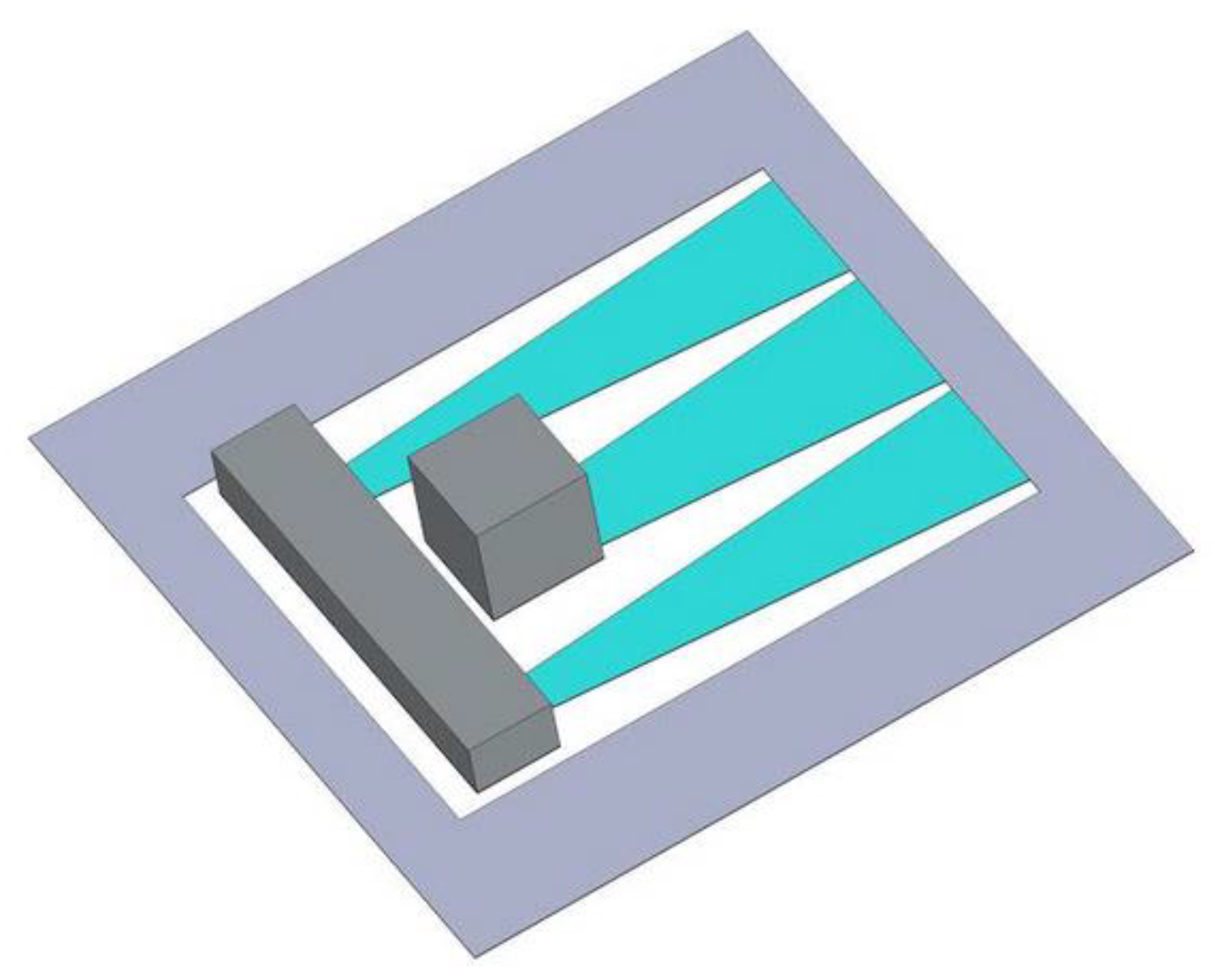
Figure 1. Schematic diagram illustrating the PEH device made in this project.
Preprints 71710 g001
Figure 2. Measurements of the micro-power generating device.
Preprints 71710 g002
Figure 3. Layers of material composing the cantilever beams of the PEH device.
Preprints 71710 g003
Figure 4. Meshing of the beams used in the simulation of this work, (a) showing the external beams device applying a mesh with 55,218 nodes, and (b) illustrating the central beam using a mesh with 55,579 nodes.
Preprints 71710 g004
Figure 5. Deformation at resonant frequencies of the microgenerator structure at the (a) center beam and (b) outer beams.
Preprints 71710 g005
Figure 6. Micromachining process by electrolysis. (a) Diagram in which the mixture of water with sodium chloride performs micromachining by electrolysis when applying a voltage of 18.5 V. (b) Image showing the micromachining moment. (c) Image captured by an optical microscope showing the substrate after the micromachining process.
Preprints 71710 g006
Figure 7. Diagram summarizing the complete process of substrate cleaning, photolithography, micromachining, and wet etching used to fabricate the PEH substrate.
Preprints 71710 g007
Figure 8. (a) Image taken before the initiation of spray deposition with the substrate positioned on the agitation rack, and (b) deposition process within a chamber constructed from recycled materials, saturated with the spray.
Preprints 71710 g008
Figure 9. Images of the deposited films taken with optical microscopy. (a) Deposit on the central beam showing the step between the substrate and the beginning of the film. (b) Multilayer film deposited on one of the outer beams, where film homogeneity is qualitatively observed.
Preprints 71710 g009
Figure 10. Results of ZnO films' transmittance percentage.
Preprints 71710 g010
Figure 11. Micrographs obtained from the piezoelectric film showing the obtaining of nanospheres. Magnified image (a) 10X times (b) 20X and (c) 30X.
Preprints 71710 g011
Figure 12. SEM micrographs were obtained on the AISI 304 steel substrate and de ZnO layer. (a) Micrograph showing the quality of the ZnO film, revealing homogeneity and freedom from visible defects on the surface, as well as a morphology that promotes adhesion to the substrate contact. (b) Image depicting the substrate thickness at 1100X magnification and a voltage of 15 kV, demonstrating significant similarity with the model proposed during FEM simulation.
Preprints 71710 g012
Figure 13. The diffractogram of ZnO films annealed at different temperatures confirms high crystallinity and preferential growth orientation, while a lower annealing temperature is recommended to prevent detachment from the substrate.
Preprints 71710 g013
Figure 14. Diffractogram of ZnO films annealed at different temperatures based on the (002) peak.
Preprints 71710 g014
Figure 15. (a) Setup of the micromachined substrate on the homemade shaker and (b) photograph of the complete vibration system featuring the micromachined substrate without deposited films.
Preprints 71710 g015
Figure 16. Experimental measurement of voltages by varying the shaker excitation frequency.
Preprints 71710 g016
Figure 17. Voltage produced by the external beams when oscillating in resonance and having random stops.
Preprints 71710 g017
Figure 18. Voltage produced by the central beam when oscillating at resonance.
Preprints 71710 g018
Figure 19. a) Power values for the center beam when performing a frequency sweep. B) Power values for external beams when performing a frequency sweep.
Preprints 71710 g019
Table 1. Voltage and power obtained by varying the load resistance of the generator at resonance.
Resistance (Ohms) Central beam voltage
(mV)
External beam voltage
(mV)
Central beam power
(µW)
External beams Power
(µW)
464000 12 34 0.00015 0.0012
200000 80 860 0.016 1.849
100000 57 560 0.0162 1.568
98000 20 70 0.0020 0.025
93449.7 43.11 503.7 0.0064 1.3574
93000 40 504 0.0086 1.3656
49500 40 230 0.0161 0.5343
Table 2. Comparison of this project with some reported works with its main characteristics.
Year Piezoelectric material Piezoelectric Film Thickness (𝜇m) Power
(𝜇W)
Frequency
(Hz)
Voltage
(mV)
Acceleration(g) Reference
2018 PVDF 200 3 6 3.7 x 10 3 - [52]
2018 PZT 60 3.5 5 4 x 10 3 1 [53]
2019 PZT 150 0.50 1.53 3 x 10 3 - [54]
2020 PVDF 28 4.9 6.1 9 x 10 3 1.5 [55]
2021 PVDF 28 0.14 25 376.92 0.24 [56]
2021 ZnO 1.5 1.97 108.84 545 2 [57]
2022 PZT 2 0.01 28.6 40 0.07 [58]
2022 Barium Titanate - 1.6 57.1 3.7 x 10 3 1 [55]
2023 PZT 500 0.000370 - 13 1 [59]
This work ZnO 1 1.849 a 35 1.08 x 10 3 a 2 External beams
This work ZnO 1 0.00016 a 58.5 180 a 2 Central beam
a Test using the shaker
Disclaimer/Publisher’s Note: The statements, opinions and data contained in all publications are solely those of the individual author(s) and contributor(s) and not of MDPI and/or the editor(s). MDPI and/or the editor(s) disclaim responsibility for any injury to people or property resulting from any ideas, methods, instructions or products referred to in the content.
Copyright: This open access article is published under a Creative Commons CC BY 4.0 license, which permit the free download, distribution, and reuse, provided that the author and preprint are cited in any reuse.
Prerpints.org logo

Preprints.org is a free preprint server supported by MDPI in Basel, Switzerland.

Subscribe

© 2024 MDPI (Basel, Switzerland) unless otherwise stated