1. Introduction
Czochralski (Cz), edge-defined, film fed growth (EFG), and Bridgeman-Stockbarger methods have been used in oxide single crystal manufacturing industries to produce bulk crystals, such as β-Ga
2O
3 [
1,
2,
3,
4,
5], LiTaO
3 (LT)[
6,
7,
8,
9], Ce:Gd
3Al
2Ga
3O
12 (GAGG) [
10,
11,
12,
13], and Ce:(Lu,Y)
2SiO
5 (LYSO)[
14,
15,
16]. Iridium (Ir) crucibles and dies are used owing to their high melting temperatures of 1900, 1650, 1850, and 2050 ºC for producing β-Ga
2O
3, LT, GAGG, and LYSO, respectively. In recent years, the sharp increase of the price of Ir metal has become a major issue in the production of these oxide crystals. In addition, a low oxygen partial pressure atmosphere is essential to prevent the loss of Ir. Raw material components, such as Ga
2O
3 and SiO
2, easily evaporate under low oxygen partial pressure, and this leads to various defect problems in the crystal [
17]. The size of the crystal is limited by the size of the crucible, particularly in the production of GAGG and LYSO scintillators, because their melting point is close to the softening point of Ir; therefore, the size limit for scintillators is a diameter of 4 inches [
13]. By using the cold crucible method, melt can be produced without a crucible, using only high-frequency power. This technique has been used for many years to produce crystals of ultra-high melting point oxides, such as cubic zirconia [
18]. However, there are issues, such as instability of the melt convection due to its excessive enhancement by high-frequency current and difficulty in controlling the optimum temperature gradient for crystal growth. This makes the convection of the melt more unstable, and it is difficult to grow large single crystals using seed crystals, such as in the Cz and EFG methods.
In this study, we proposed a new crucible-free crystal growth method, namely, oxide crystal growth from a cold crucible (OCCC), and attempted to grow 2-inch diameter β-Ga
2O
3 single crystals without Ir crucible under various oxygen partial pressure atmosphere. In the OCCC method, as in the cold crucible method, a high frequency is applied directly to the oxide material, which is heated and melted; the outermost solid material itself is used as a crucible to hold the melt and it is cooled with water using a copper hearth. High frequencies in the range of hundreds of kHz to MHz are required considering the resonance frequency for the oxide melt. In the first stage of this study, we measured the electrical resistivity of the oxide melt, set the frequency that resulted in the appropriate high-frequency penetration depth and temperature gradient, and prototyped a high-frequency oscillator and crystal growth furnace. β-Ga
2O
3 is a well-known semiconductor material for power devices and other equipment. Recently β-Ga
2O
3 has also been reported as a scintillator material with light yields of approximately 8400 ph./MeV, scintillation decay time of <1 μs, and density of 6.44 g/cm
3 [
1]. In this study, β-Ga
2O
3 single crystals were grown by oxide crystals using the cold crucible (OCCC) method under various oxygen partial pressures. The optical properties and radiation responses of the crystals grown under various oxygen partial pressures were evaluated.
2. Materials and Methods
2.1. Development of the Oscillator and Crystal Growth Technology
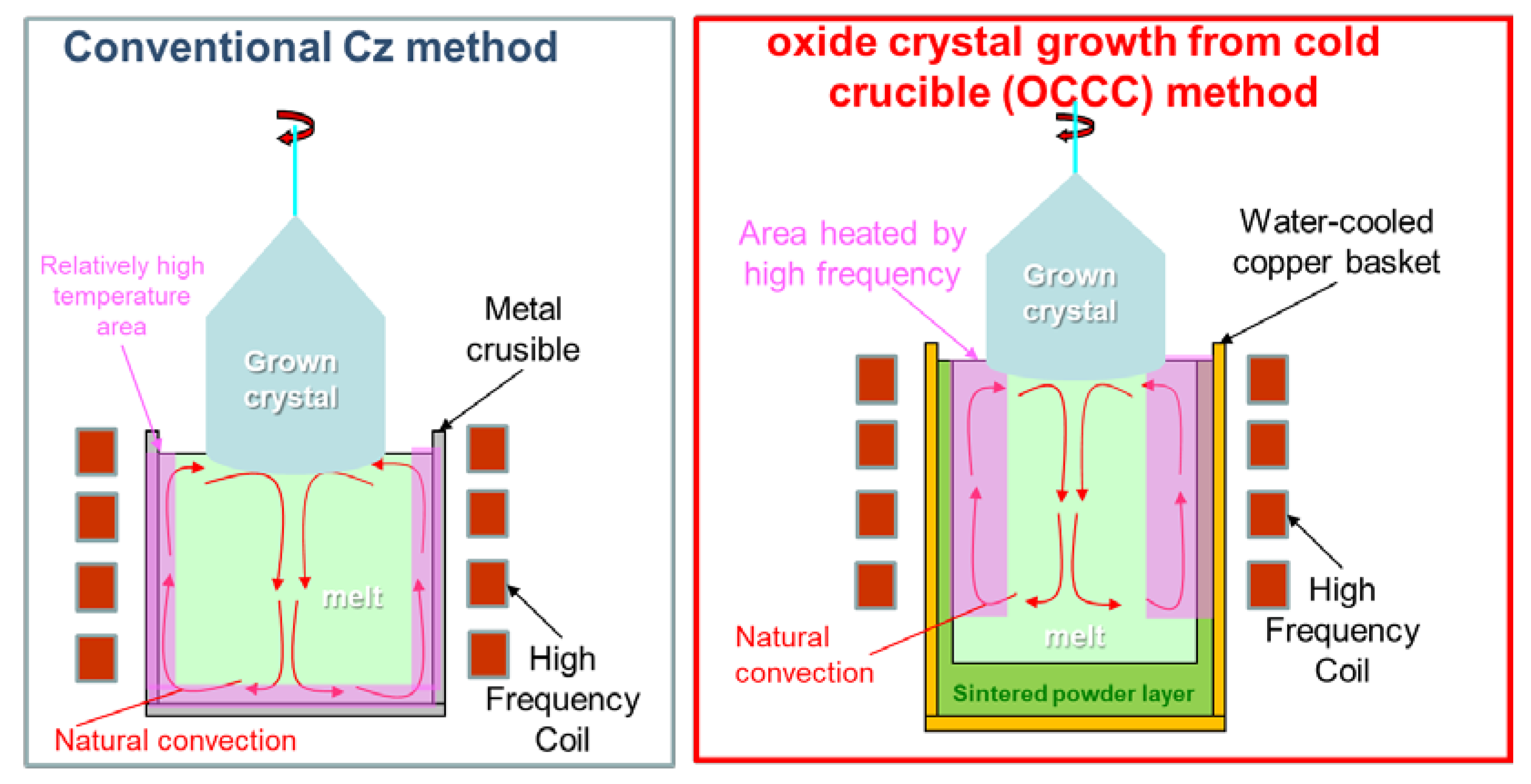
Figure 1 shows a schematic diagram of the heating region and melt convection in the conventional Cz and OCCC methods. Controlling the temperature gradient in the melt is necessary for high-quality crystal growth. In the Cz method using an Ir crucible that is heated by high-frequency heating, the temperature gradient is formed toward the center of the upper surface of the melt, thereby generating natural convection from the periphery of the melt toward the center of the upper surface. This facilitates controlling the crystal diameter using a seed. In the OCCC method, as in the cold crucible method, a high frequency is applied directly to the oxide material, which is heated and melted; the outermost solid material itself is used as a crucible to hold the melt and it is cooled by water using a copper hearth. To realize a similar melt temperature gradient and natural convection in the OCCC method as in the Cz method, it is important to control the high-frequency penetration depth in the melt, as mentioned above. The relationship between the depth δ of the magnetic field penetrating the heated object and the frequency
is as follows: (
: intrinsic resistance (μΩ·cm) and
: specific permeability)
At the beginning of this study, the electrical resistivity of the gallium oxide melt was measured to set the frequency to achieve an appropriate penetration depth.
Figure 2 shows a schematic diagram of the melt electrical resistivity measurement using an Ir crucible and a rod. Measurements were performed using the AC two-terminal method [
19]. An Ir crucible with an inner diameter of 48 mm and a height of 50 mm was filled with gallium oxide raw material and melted by high-frequency heating, and an Ir rod with a diameter of 2 mm was buried at the center of the melt at a predetermined depth. The electrical resistance value of the oxide melt r [Ω] is shown in Eq. 2. (
: measured voltage values,
: 50 Ω of electrical resistance)
The electrical resistivity of the oxide melt
ρ [Ωm] is shown in Eq. 3-5. (
: volume of Ir rod that is partly buried in the melt,
diameter of the Ir rod,
inner diameter of the Ir crucible,
: distance between the Ir rod and crucible)
The temperature of the melt surface was observed using a radiation thermometer and an Ir-IrRh thermocouple placed in the melt. After melting, the Ir rod was lowered by a specified distance and buried in the melt. The electrical resistivity was calculated from the measured voltage values at each temperature. The temperature of the melt surface was observed using a radiation thermometer and an Ir-IrRh thermocouple placed in the melt. After melting, the Ir rod was lowered by 15 mm and buried inside the melt. The electrical resistivity was calculated from the measured voltage values of
at each temperature.
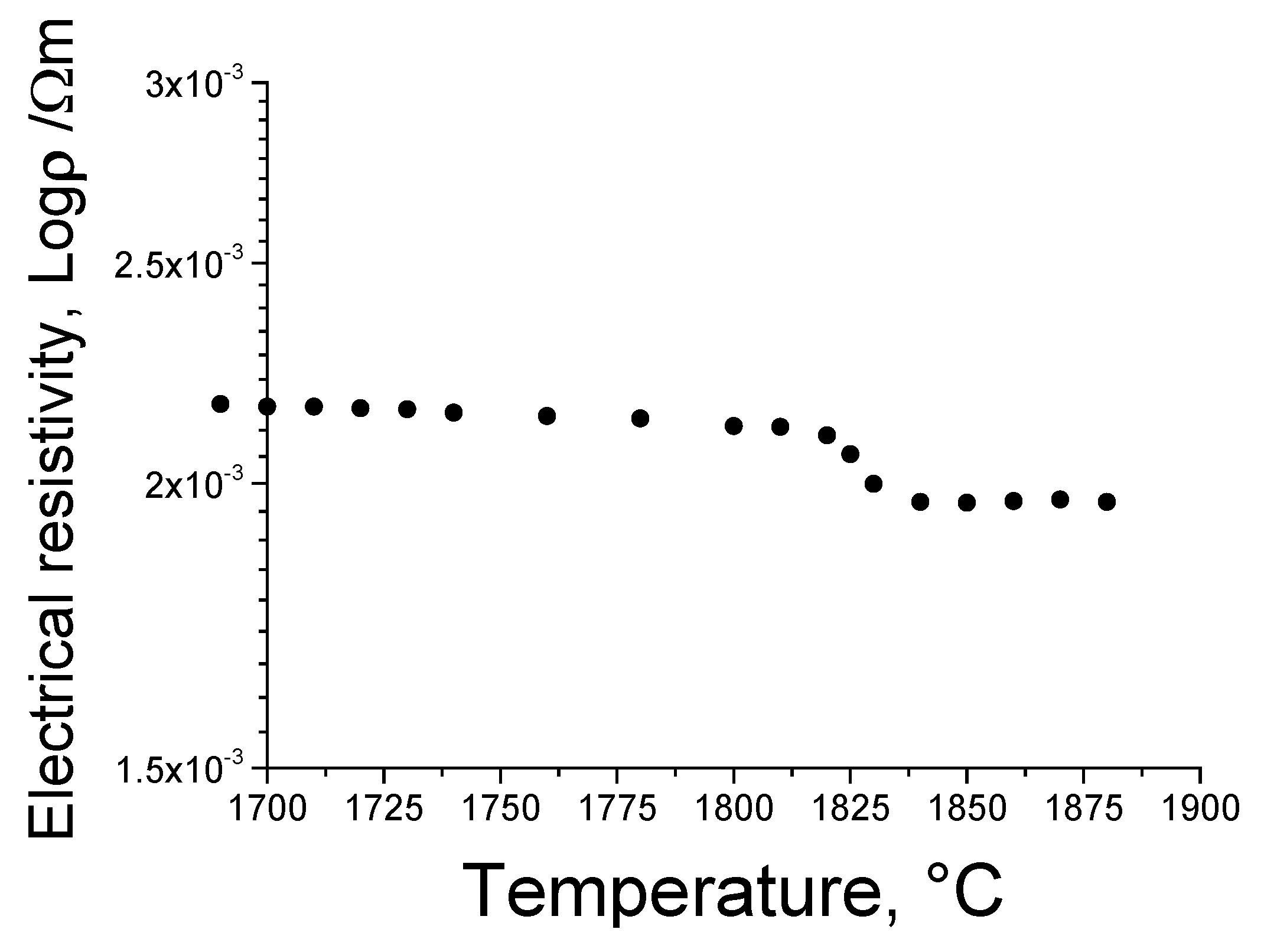
Figure 3 shows the temperature dependence of the electrical resistivity of the melt and solidified Ga
2O
3. The melt began to solidify at approximately 1840 °C. The electrical resistivity was 1.96 x 10
-3 Ωm for the melt at 1880 °C and 2.12 x 10
-3 Ωm for the solid at 1800 °C. This was lower than 2.60 x 10
-3 Ωm for the Al
2O
3 melt [
19].
A water-cooled copper basket with an inner diameter of 100 mm and height of 60 mm was prepared for the growth of a 50 mm diameter crystal from a 100 mm diameter melt. Oscillator modules consisting of a SiC metal-oxide-semiconductor field-effect transistor were prototyped, and direct heating of the Ga2O3 melt was achieved using a work coil with a diameter of 140 mm and oscillator modules. The details of the oscillator module circuit are omitted because they are commercially and technically confidential information.
β-Ga2O3 (5N purity, Iwatani Corp, Japan.) powder was prepared as the starting material and used to fill the basket. The crystal growth setup was covered with an atmosphere-controllable chamber, and crystals were grown in atmospheres with different oxygen partial pressures. The typical growth rate was 3 mm/h, and β-Ga2O3 single crystals with 30-50 mm diameter were grown using <010> oriented β-Ga2O3 seeds. The as-grown crystals were cut into plates of 1 mm thickness and polished for the measurements.
2.2. Evaluation of the Optical Properties and Radiation Responses
Transmittance spectra were measured with the JASCO V550 spectrophotometer in the 190-750 nm range. Radioluminescence (RL) spectra were obtained under X-ray excitation using an Andor Technology SR-163 spectrometer equipped with an Andor Technology iDus420-OE charge-coupled device detector. Pulse height spectra were measured using a Hamamatsu R7600U-200 photomultiplier tube (PMT). The samples were optically coupled to PMT using silicone grease. The measured sample was covered with Teflon tape. The output signal was fed via an ORTEC 572A shaping amplifier and a two-channel USB WaveCatcher module into a personal computer. The decay curve was obtained using the same PMT. The output signal was recorded using a Tektronix TD5032B digital oscilloscope.
3. Results and Discussion
3.1. Crystal Growth
Figure 3 shows the temperature dependence of the electrical resistivity of the melt and solidified Ga
2O
3. The melt began to solidify at approximately 1840 °C. The electrical resistivity was 1.96 x 10
-3 Ωm for the melt at 1880 °C and 2.12 x 10
-3 Ωm for the solid at 1800 °C. This was lower than 2.60 x 10
-3 Ωm for the Al
2O
3 melt [
19]. To set a high-frequency penetration depth of approximately 35 mm for a melt with diameter of 100 mm, the specific permeability was assumed to be 1 in Eq. (1) and an oscillator was designed with a frequency of 400 kHz.
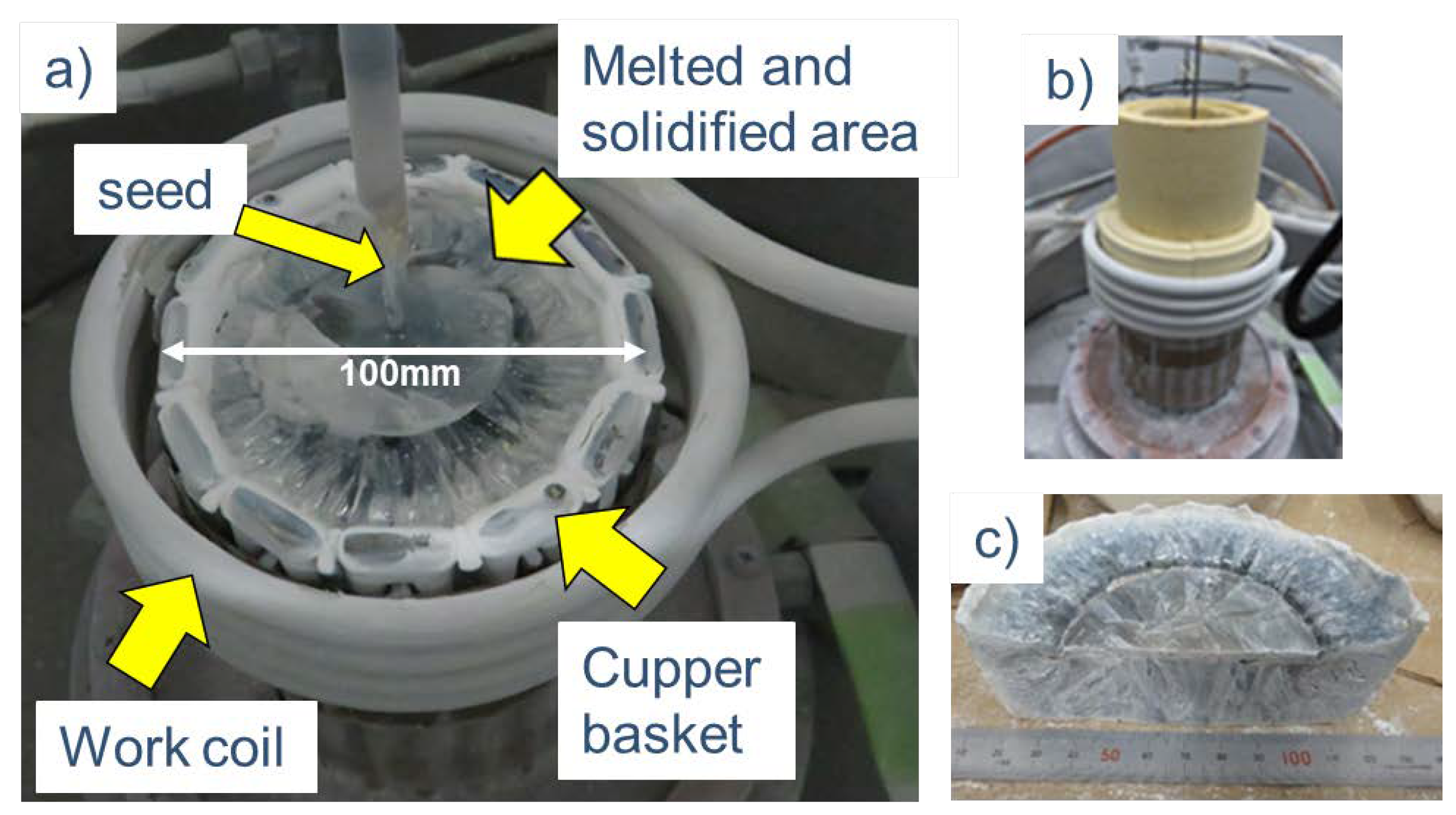
Figure 4 shows photographs of the setup after the crystal growth, the setup with the heat-insulating material during heating, and a photograph of the residual melt removed from the basket and cut. The basket and the melt were separated by a 2-3 mm raw material powder layer and were melted according to the shape of the basket, while there was no direct contact between them.
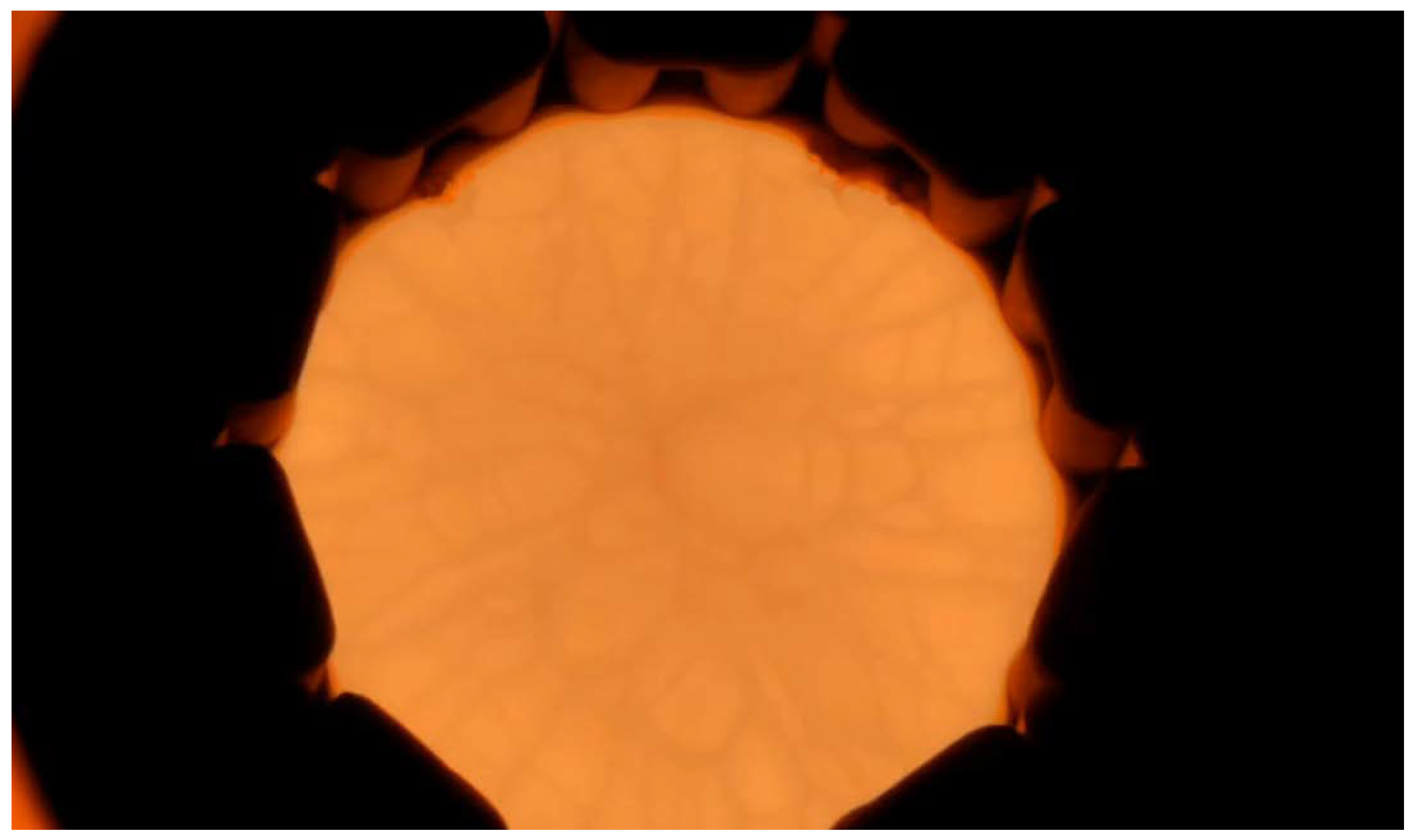
Gallium (Ga) metal was placed on the powder raw material filled in the basket, and high-frequency heating was performed. When Ga metal was first heated and reached the melting point of gallium oxide, the surrounding gallium oxide melted, and the molten region gradually expanded. Finally, the Ga metal was oxidized and disappeared, and only the melt was heated by high-frequency induction. After being left for 1 h or longer, the melt expanded throughout the interior of the basket, and a spoke pattern was confirmed on the surface of the melt, as shown in
Figure 5. It is thought that convection flows from the outer periphery of the melt toward the center. Subsequently, seeding was performed, and pulling up started. While visually confirming the diameter, the oscillator output was manually adjusted to increase the crystal diameter. A photograph of the β-Ga
2O
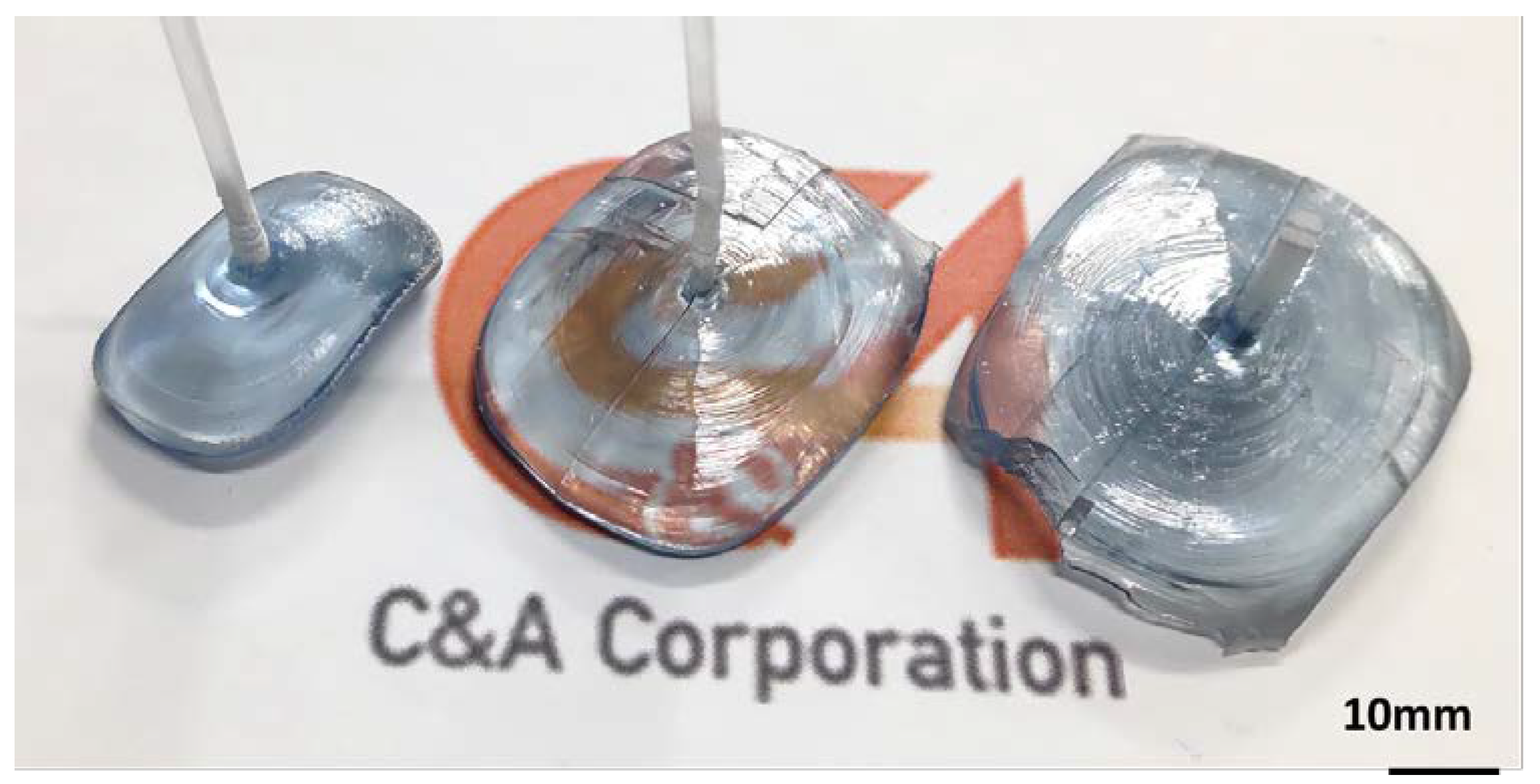
3 single crystals grown in air is shown in
Figure 6. Pale blue crystals with a diameter of 30-50 mm and a body length of 5-10 mm were obtained. When the amount of melt in the basket decreased, the high-frequency heating became unstable. In addition, owing to restrictions on manual control, the crystal length was limited to such a short length that can be stably produced. Impurity analysis of the crystals grown in air was performed by glow discharge mass spectrometry (GDMS). The analysis results are shown in
Table 1, along with the impurity analysis data for the β-Ga
2O
3 raw powder. The concentrations of Cu in the basket material and Zr in the zirconia insulator were sufficiently low, and it is considered that there was no contact with the melt of the basket or the heat-insulating material. However, the Si concentration in the grown crystal was relatively high at 11 ppm, which is considered to be derived from the raw powder. In this study, it was demonstrated that crystal growth by melt direct induction heating without a crucible is possible. This new crystal growth technique was named the OCCC method. The region and depth of the melt to be heated can be changed by changing the frequency and coil position. Based on these parameters, the convection and temperature gradient of the melt can be controlled, and stable crystal growth through the process of seeding and crystal diameter expansion are major features of this method. Automatic diameter control using weight sensors and images and increasing the length and size of the crystals will be explored in future research.
3.2 Optical Properties and Radiation Responses
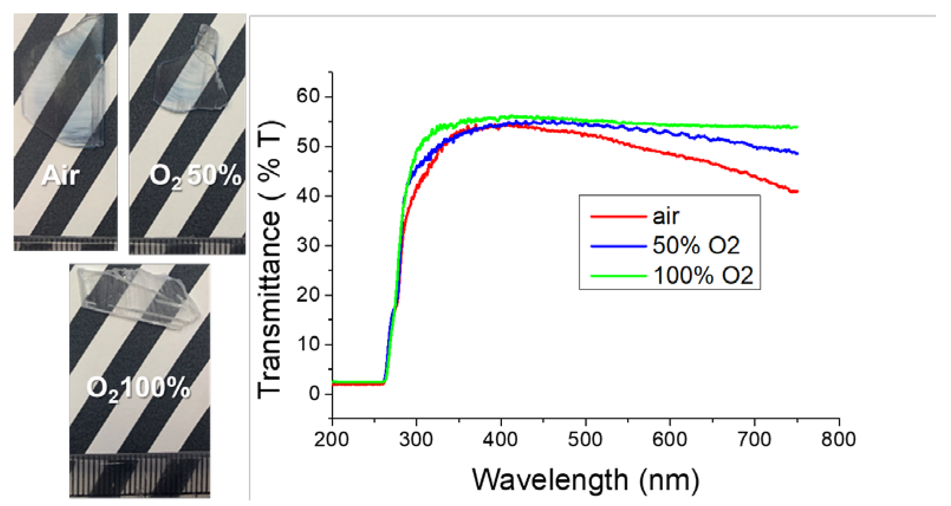
Figure 7 shows photographs of the β-Ga
2O
3 plates grown in atmospheres of air, Ar + 50% O
2, and 100% O
2 in air and their transmittances. It was confirmed that the higher the oxygen partial pressure during growth, the more colorless and transparent were the crystals. As the partial pressure of oxygen decreased, the transmittance decreased at the absorption edge near 310 nm. Even in the region above 450 nm, crystals grown under a high oxygen partial pressure tended to have high transmittance.
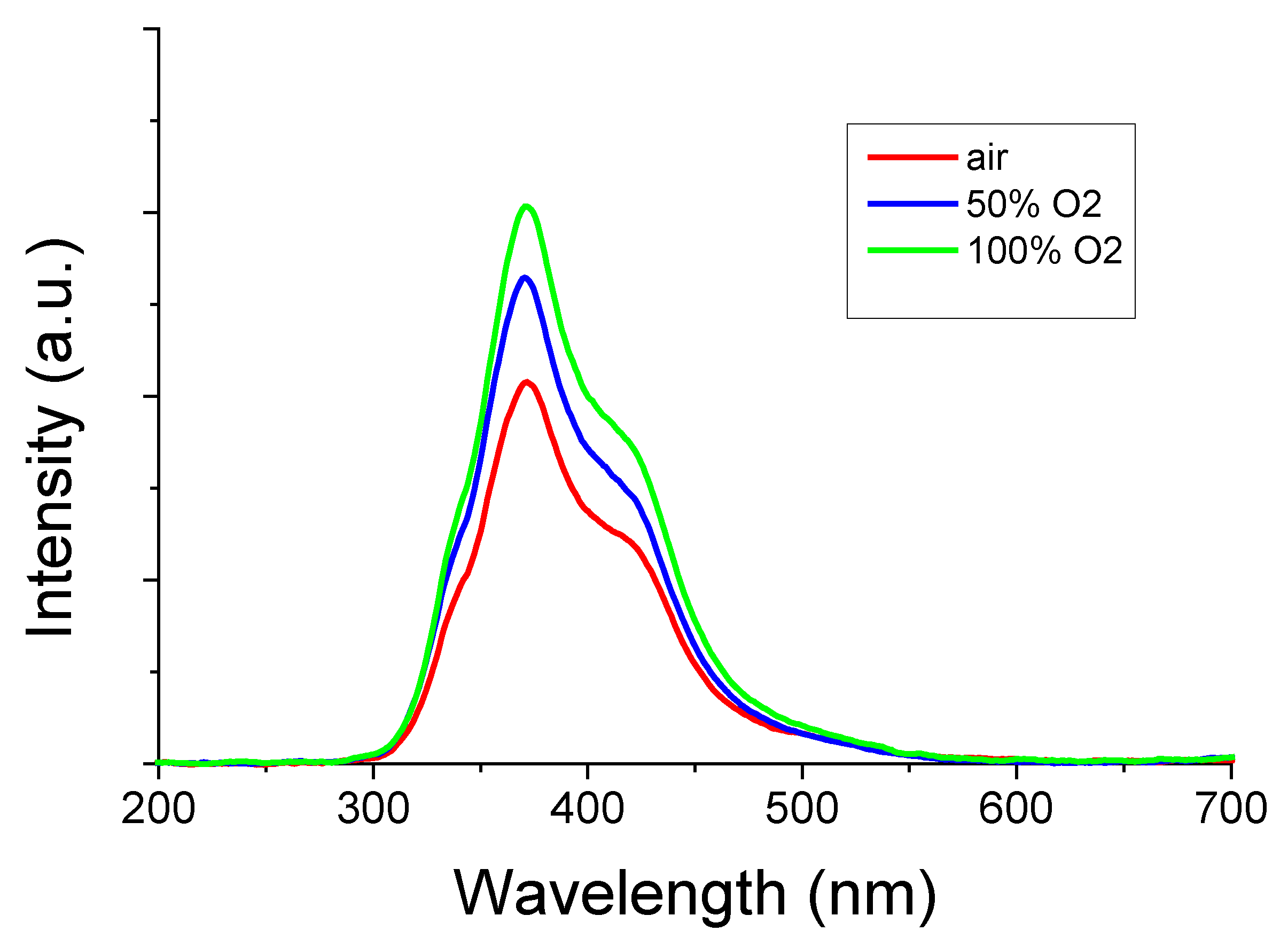
Figure 8 shows the RL spectra of the β-Ga
2O
3 plates grown under each oxygen partial pressure. Similar to previous studies, the host emission peaking at 380 nm was confirmed [
20]. The higher the oxygen partial pressure, the higher the luminescence intensity.
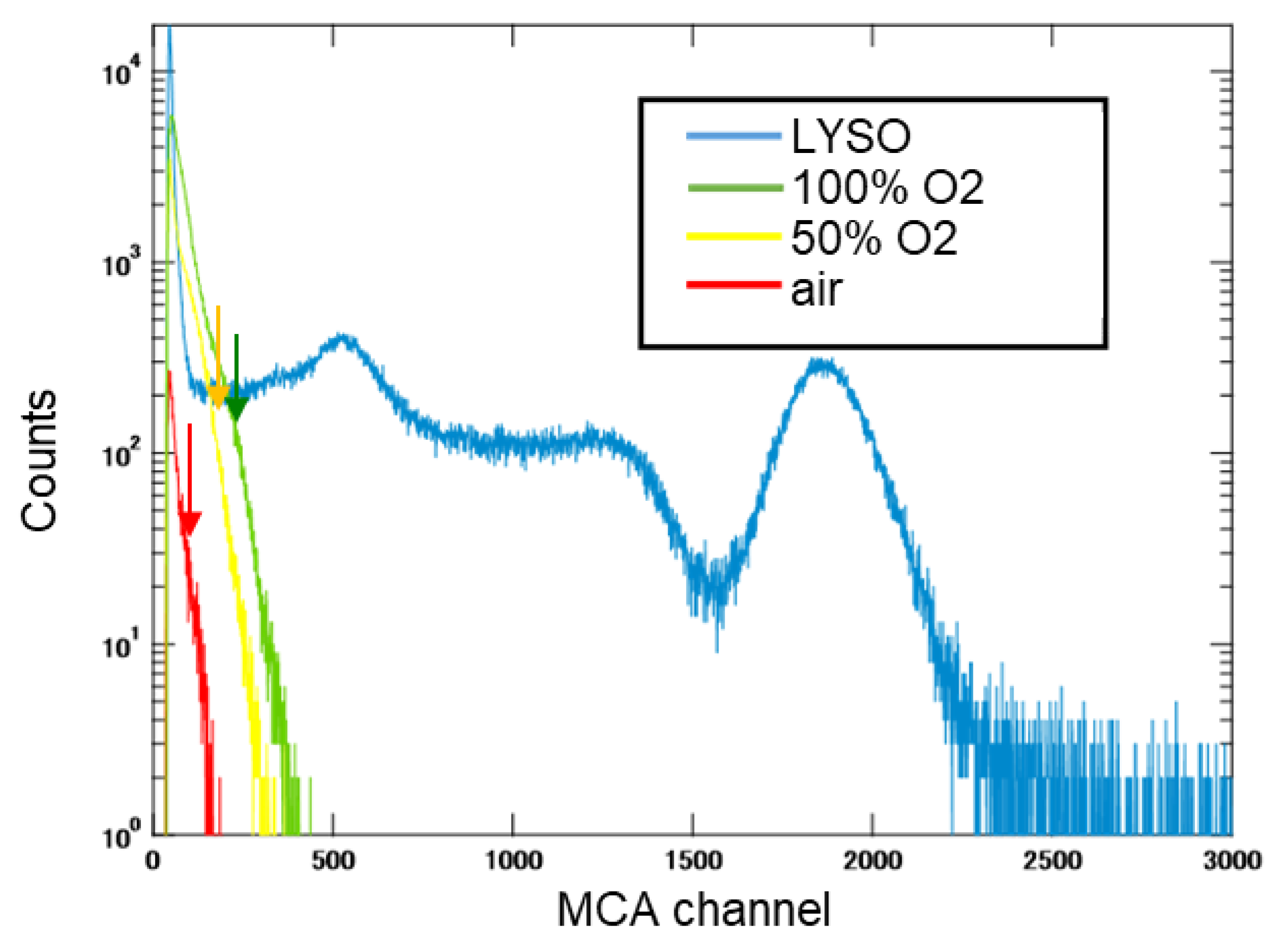
Figure 9 shows the pulse height spectra of the β-Ga
2O
3 plate samples irradiated by 662 keV gamma-ray using a
137Cs source. The light outputs of the β-Ga
2O
3 samples were calculated by comparing the positions of the photo absorption peaks with the LYSO standard, which has a reported light output of 33,800 photons/MeV. Because a clear photoelectric absorption peak could not be confirmed for β-Ga
2O
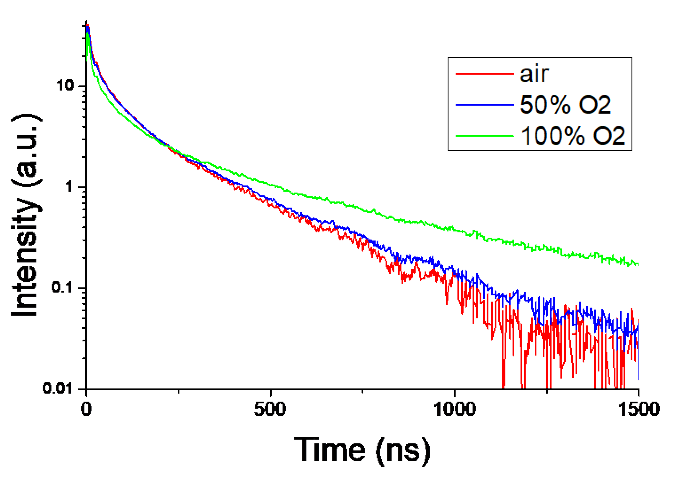
3, the light outputs were calculated by the channel position indicated by the arrows as the photoelectric absorption peak using each Gaussian fitting. The wavelength dependence of the quantum efficiency of the PMT was considered for correction. (42%@380 nm, 38%@420 nm). Scintillation decay curves were obtained using the PMT and digital oscilloscope, and the sample was irradiated by 662 keV gamma-ray (
Figure 10). The decay time was approximated using Eq. (2), which is the sum of the three exponents:
Table 1 summarizes the light output and decay time of each sample. The light outputs were 4,000-1,300 photons/MeV, and the decay times of the three components were confirmed. Previous literature has reported that the higher the free electron concentration, the lower the light output and the shorter the decay time [
21]. Although there are no data on the actual Si concentration in the crystal, it has also been reported that intentional Si addition increases the free electron concentration. The grown crystals contained a relatively high concentration of Si derived from the raw powder and were expected to have a high free electron concentration. The light output and decay time of the 100% oxygen sample are comparable to those of Si-doped β-Ga
2O
3 crystals in the literature, and Si in the raw material may be the cause. In addition, it is known that there is a correlation between the free electron concentration and oxygen vacancies, and the oxygen vacancies of β-Ga
2O
3 may be suppressed when the oxygen partial pressure in the growth atmosphere is high [
22]. Because oxygen vacancies can be reduced by increasing the oxygen partial pressure during growth, the free electron concentration may decrease, and the light output may increase. Measurement of the free electron concentration is an interesting topic for further study. The theme of this research is the development of a new crucible-free crystal growth technology and growth equipment. Furthermore, we believe that the successful growth of 2-inch-sized β-Ga
2O
3 single crystals is an important achievement.
Table 2.
Light yield and decay time of the β-Ga2O3 plates.
Table 2.
Light yield and decay time of the β-Ga2O3 plates.
4. Conclusions
In this research, we proposed OCCC as a new crystal growth technology that does not use a crucible and succeeded in growing a 2-inch size β-Ga2O3 single crystal. To directly heat the melt by high-frequency induction heating, the electrical resistivity of the β-Ga2O3 melt was measured, and an oscillator with the optimum frequency was prototyped considering the high-frequency penetration depth. Furthermore, the crystals were grown under various oxygen partial pressures and their transmittance and radiation response characteristics were evaluated. At present, crystals with approximately 10 mm length have been obtained. We are developing a device with a sufficiently deep basket and movable work coil. By following the increase in volume of the growing crystal and maintaining the melt volume constant, we will be able to continue pulling the crystal stably and grow longer crystals. Furthermore, automatic crystal diameter control by a weight sensor and image analysis are under consideration.
In recent years, the price of Ir, which is a precious metal, has soared, and the price of an 8-inch crucible for producing a 4-inch crystal has exceeded 100 million dollars. This problem is a major obstacle to the continuation, development, and expansion of business in the production of oxide crystals. If the OCCC method can be applied to the production of existing oxide crystals, such as LT, GAGG, and LYSO, productivity can be greatly improved.
Author Contributions
Conceptualization, K. Kamada, V.K., K. Kakimoto, and A.Y.; methodology, T.T., Y.S., and I. T.; formal analysis, R.Y., T.H., and M.Y.; investigation, R.Y., T.H., and M.Y.; writing—original draft preparation, K. Kamada; writing—review and editing, K. Kamada, V.K., K. Kakimoto, and A.Y.; supervision, A.Y.; project administration, K. Kamada.; funding acquisition, K. Kamada. All authors have read and agreed to the published version of the manuscript.
Funding
A part of this research was financially supported by Japan Society for the Promotion of Science, KAKENHI, grant numbers; 18H01222, 19H00672, 19K12626, 19H00881, 19K12626, 20K20488, 22H04961.
Data Availability Statement
Not applicable
Acknowledgments
We would like to thank Editage (
www.editage.com) for English language editing.
Conflicts of Interest
The authors declare no conflict of interest. The funders had no role in the design of the study; in the collection, analyses, or interpretation of data; in the writing of the manuscript; or in the decision to publish the results.
References
- Tomm, Y.; Reiche, P.; Klimm, D.; Fukuda, T.J. Czochralski grown Ga2O3 crystals. Cryst. Growth 2000, 220, 510–514. [Google Scholar] [CrossRef]
- Aida, H.; Nishiguchi, K.; Takeda, H.; Aota, N.; Sunakawa, K.; Yaguchi, Y. Growth of β-Ga2O3 single crystals by the edge-defined, film fed growth method. Japan. J. Appl. Phys. 2008, 47, 8506–8509. [Google Scholar] [CrossRef]
- Galazka, Z.; Uecker, R.; Klimm, D.; Irmscher, K.; Naumann, M.; Pietsch, M.; Kwasniewski, A.; Bertram, R.; Ganschow, S.; Bickermann, M. Scaling-up of bulk β-Ga2O3 single crystals by the Czochralski method. ECS J. Solid State Sci. Technol. 2017, 6(2), Q3007–Q3011. [Google Scholar] [CrossRef]
- Kuramata, A.; Koshi, K.; Watanabe, S.; Yamaoka, Y.; Masui, T.; Yamakoshi, S. High-quality β-Ga2O3 single crystals grown by edge-defined film-fed growth. Jpn. J. Appl. Phys. 2016, 55(12), 1202A2. [Google Scholar] [CrossRef]
- Hoshikawa, K.; Kobayashi, T.; Ohba, E. 50 mm diameter Sn-doped (0 0 1) β-Ga2O3 crystal growth using the vertical Bridgeman technique in ambient air. J. Cryst. Growth 2020, 546, 125778. [Google Scholar] [CrossRef]
- Abrahams, S.C.; Bernstein, J.L. Ferroelectric lithium tantalate—1. Single crystal X-ray diffraction study at 24°C. J. Phys. Chem. Solids 1967, 28, 1685–1692. [Google Scholar] [CrossRef]
- Fukuda, T.; Matsumura, S.; Hirano, H.; Ito, T. Growth of LiTaO3 single crystal for SAW device applications. J. Cryst. Growth 1979, 46(2), 179–184. [Google Scholar] [CrossRef]
- Furukawa, Y.; Kitamura, K.; Suzuki, E.; Niwa, K. Stoichiometric LiTaO3 single crystal growth by double crucible Czochralski method using automatic powder supply system. J. Cryst. Growth 1999, 197(4), 889–895. [Google Scholar] [CrossRef]
- Kitamura, K.; Furukawa, Y.; Niwa, K.; Gopalan, V.; Mitchell, T. E. Crystal growth and low coercive field 180 domain switching characteristics of stoichiometric LiTaO3. Appl. Phys. Lett. 1998, 73(21), 3073–3075. [Google Scholar] [CrossRef]
- Kamada, K.; Yanagida, T.; Endo, T.; Tsutumi, K.; Fujimoto, Y.; Fukabori, A.; Yoshikawa, A.; Pejchal, J.; Nikl, M. Composition engineering in cerium-doped (Lu, Gd)3(Ga, Al)5O12 single-crystal scintillators. Cryst. Growth Des. 2011, 11, 4484–4490. [Google Scholar] [CrossRef]
- Kamada, K.; Shoji, Y.; Kochurikhin, V.V.; Okumura, S.; Yamamoto, S.; Nagura, A.; Yeom, J.Y.; Kurosawa, S.; Yokota, Y.; Ohashi, Y.; Nikl, M.; Yoshikawa, A. Growth and scintillation properties of 3 inch diameter Ce doped Gd3Ga3Al2O12(GAGG) single crystal scintillator. J. Crys. Growth 2016, 452, 81–84. [Google Scholar] [CrossRef]
- Kamada, K.; Yanagida, T.; Pejchal, J.; Nikl, M.; Endo, T.; Tsutumi, K.; Usuki, Y.; Fujimoto, Y.; Fukabori, A.; Yoshikawa, A. Crystal growth and scintillation properties of Ce doped Gd3(Ga,Al)5O12 single crystals. IEEE Trans. Nucl. Sci. 2012, 59, 2112–2115. [Google Scholar] [CrossRef]
- Kochurikhin, V.; Kamada, K.; Kim, K.J.; Ivanov, M.; Gushchin, L.; Shoji, Y.; Yoshino, M.; Yoshikawa, A. Czochralski growth of 4-inch diameter Ce:Gd3Al2Ga3O12 single crystals for scintillator applications. J. Cryst. Growth 2020, 531, 125384. [Google Scholar] [CrossRef]
- Melcher, C.L.; Schweitzer, J.S. Cerium-doped lutetium oxyorthosilicate - a fast, efficient new scintillator. IEEE Trans. Nucl. Sci. 1992, 39, 502–505. [Google Scholar] [CrossRef]
- Melcher, C.L.; Schweitzer, J.S.; Peterson, C.A.; Manente, R.A.; Suzuki, H. Crystal growth and scintillation properties of the rare earth orthosilicates. In Inorganic Scintillators and Their Applications; Delft Unviersity Press (SCINT95), 1996; pp. 309–315. ISBN 90-407-1215-8. [Google Scholar]
- Spurrier, M.A.; Szupryczynski, P.; Yang, K.; Carey, A.A.; Melcher, C.L. Effects of Ca2+ Co-doping on the scintillation properties of LSO:Ce. IEEE Trans. Nucl. Sci. 2008, 55, 1178–1182. [Google Scholar] [CrossRef]
- Hajnal, Z.; Miró, J.; Kiss, G.; Réti, F.; Deák, P.; Herndon, R.C.; Kuperberg, J.M. Role of oxygen vacancy defect states in the n-type conduction of β-Ga2O3. J. Appl. Phys. 1999, 86, 3792–3796. [Google Scholar] [CrossRef]
- Kaldis, E. Current Topics in Material Science; North-Holland, 1978; Vol. 1, Chapter 6; p. 421. [Google Scholar]
- Fay, H. The electrical conductivity of liquid Al2O3 (molten corundum and ruby). J. Phys. Chem. 1966, 70, 890–893. [Google Scholar] [CrossRef]
- Yanagida, T.; Okada, G.; Kato, T.; Nakauchi, D.; Yanagida, S. Fast and high light yield scintillation in the Ga2O3 semiconductor material. Appl. Phys. Express 2016, 9, 042601. [Google Scholar] [CrossRef]
- Drozdowski, W.; Makowski, M.; Bachiri, A.; Witkowski, M.E.; Wojtowicz, A.J.; Swiderski, L.; Irmscher, K.; Schewski, R.; Galazka, Z. Heading for brighter and faster β-Ga2O3 scintillator crystals. Opt. Mater.: X 2022, 15, 100157. [Google Scholar] [CrossRef]
- Pan, X.; Yang, M.-Q.; Fu, X.; Zhang, N.; Xu, Y.-J. Defective TiO2 with oxygen vacancies: synthesis, properties and photocatalytic applications. Nanoscale 2013, 5, 3601–3614. [Google Scholar] [CrossRef] [PubMed]
|
Disclaimer/Publisher’s Note: The statements, opinions and data contained in all publications are solely those of the individual author(s) and contributor(s) and not of MDPI and/or the editor(s). MDPI and/or the editor(s) disclaim responsibility for any injury to people or property resulting from any ideas, methods, instructions or products referred to in the content. |
© 2023 by the authors. Licensee MDPI, Basel, Switzerland. This article is an open access article distributed under the terms and conditions of the Creative Commons Attribution (CC BY) license (http://creativecommons.org/licenses/by/4.0/).

