
You are currently viewing a beta version of our website. If you spot anything unusual, kindly let us know.
Preprint
Communication
A Study on Electrothermal Characteristics of ESD Protection Devices Based on ggNMOS
Altmetrics
Downloads
147
Views
37
Comments
0

This version is not peer-reviewed
Abstract
To study the influence of electrothermal effect of ESD protection device on the reliability of inte-grated circuit,a theoretical model of ESD protection device thermal resistance is constructed in the paper based on the Conservation of Energy Principle. By analyzing the temperature relativity between electricity parameter and thermology parameter of ESD protection device characterized by self-heating thermal resistance, the quantitative relationship expression of physical parameter and geometric parameter is obtained, which can be used to improve ESD protection device elec-tro-thermal effect. The simulation testing and the real tape-out testing of ESD protection device self-heating thermal resistance based on ggNMOS are shown and compared. It is concluded that self-heating thermal resistance is an effective index for the protection device electrothermal char-acterization. Based on the established model, the self-heating thermal resistance could be decreased to improve the homogeneity of the heat transference. The uneven distribution of device temperature can be reduced, and the overall reliability of chips can be improved.
Keywords:
Subject: Physical Sciences - Applied Physics
1. Introduction
With the continuous improvement of integrated circuit design technology and production process level, the characteristic size of ESD protection devices is continuously shrinking. The increase in unit area protection device integration inevitably brings about heat dissipation problems, which have increasingly attracted the attention of the integrated circuit industry and related scientific research institutions regarding reliability and thermal failure issues. Therefore, some researchers in academia have shifted the research focus from ESD electrical properties to electric-thermal properties, in-depth research on the physical formation mechanism of protective device electric-thermal effects, proposed methods and measures to reduce and mitigate electric-thermal effects, and hoped to open up a way to solve chip reliability problems from the perspective of ESD electric-thermal properties research. This research idea and method have significant implications for the overall reliability of chips and have practical technological and economic value. As the electrostatic discharge (ESD) [1] protection device is extensively applied on various analog integrated circuit chips [6], RF integrated circuit chips and mixed-signal integrated circuit chips, its thermal stability has become a critical issue. Despite having good electrical properties, ESD protection device generate a rapid rise in lattice temperature [2] when discharging transient high-voltage large-current electrostatic pulses via a single device or device combination. The ESD protection device generates certain heat within a brief time () and limited space ()that causes the electrical parameters of the protected core circuit to drift, which can degrade the rated safe operating range of the core circuit. This may cause the failure of the protected core circuit and lead the occurrence of the irreversible heat dissipation. This mechanism that device temperature rises due to the dissipation power of the ESD protection device is called the electrothermal effect of protection devices. The electrothermal effect has great influence on the ESD protection device and the protected core circuit. This would degrade the normal operation of chips.
In order to study the electrothermal effect of the ESD protection device and also optimize the electrical properties and safe operating area of the core circuit for withstanding external sudden pulse events, people usually adopt thermal resistance as an effective indicator to measure the electrothermal effect of the ESD protection device [7]. Thermal resistance includes ESD self-heated thermal resistance and coupling thermal resistance. Self-heated thermal resistance, mainly determined by the resistance, capacitance and parasitic effect parameters of the protection device, reflects the temperature correlation of the electrical indicators of the ESD protection device and is an effective physical quantity for representing the thermal stability of the ESD protection device. Meanwhile, when the core circuit is operating, power dissipated by its own devices and circuits will also generate certain heat, and the heat generated by the core circuit and the ESD protection device is conducted mutually to cause uneven chip temperature distribution. The thermal resistance for measuring this mutual heat transfer relationship is called coupling thermal resistance.
Due to limitations of technologies and test techniques, the influence of coupling thermal resistance on the electrical parameters of the ESD protection device is ignored here. Along with progress in integrated circuit technologies, the feature size of devices is decreasing constantly, the current density of core circuit is doubled, and SOI technique and dielectric materials are continuously applied to device separation technique, which constantly increase thermal resistance. As a result, the influence of electrothermal effect on chip performance is further intensified. The reliability of the ESD protection device is reduced, and the normal operation of the core circuit is affected. However, because the ESD protection device has diversified structures and poor technological portability currently, there is no general explanation with clear physical significance on relationship between the thermal resistance and electrical parameters and geometric parameters of the ESD protection device.
This paper puts forward a method for calculating the self-heated thermal resistance of ESD protection device based on grounded-gate NMOS (ggNMOS) structure according to the energy conservation law and studies measures for improving the electrothermal effect of ESD protection device. When the core circuit operates normally, a quantitative description is given to correlation among the electrical parameters, geometric parameters and thermal parameters of the ESD protection device by establishing a theoretical model for the thermal resistance of the ESD protection device, and used as an effective reference indicator for increasing the thermal stability of the ESD protection device.
2. Theoretical Model
Figure 1 illustrates the structural diagram of active zone of ggNMOS-based [3] protection device. As the feature size of the device enters deep submicron order, the size of the ESD protection device is very small, and the heating range of the active zone of the device can be equivalent to a parallelepiped [6]. The length, width and height (thickness) of the active zone of the protection device are respectively assumed as b, a and c. The thickness is determined by the technological level of the chip manufacturer and material properties and is usually a fixed constant, so heat source of the active zone of the protection device can be equivalent to a rectangular heat source unit [6]. Because the dimensions of the equivalent rectangular unit are within submicron range, assuming that thermal balance is basically kept between internal and external temperatures of the rectangular unit, the temperature in the center of the rectangular unit can be used for representing the temperature of this active heating region [6].
During normal operating, the ESD protection device is stationary, and the temperature is known T0. When an ESD event occurs, the protection devices suppresses high voltage and discharges high current, heat will be generated inside, and its power is Q0. Meanwhile, partial area As on the outer surface of the ESD protection device is exposed in the chip tube with temperature Tf, the surface coefficient of heat transfer between chip and tube is α, and the object volume of the heat conducting zone of the protection device is V0. The heat generating process inside the ESD protection device follows the energy conservation law:
{Heat entering ESD protection device} + {heat generated by ESD protection device itself} = {Heat discharged from ESD protection device} + {Change of heat stored in ESD protection device}, i.e.:
Hi + Hg = Ho + Hs,
Hi is the heat generated by ESD event, usually a product of voltage and current of human body discharge model (HBM) [10] and a constant Qi; Hg is thermal energy generated by ESD protective device varying with time according to:
Hg = Q0e-βτ,
Ho is the heat transiently transferred by ESD protection device, i.e.:
Ho = αAs(Tj - Tf),
Tj is the internal transient peak temperature of ESD protection device; Hs is the change rate of heat stored in ESD protection device, i.e.:
Substitute the above variables into formula (1) to obtain
Define
ϕ = αAs / mcp,θ = Tj - Tf,
Then formula (5) is transformed into
When intitial conditions: τ = 0, T0 = Tf are substituted into formula (6),
According to JEDEC standard No. 51-1, the self-heated thermal resistance of ESD protection device is defined as
Tj is junction temperature of the device during transient operation, Tf is reference temperature, and PH is power dissipated to the device in the form of heat.
Substitute the above parameters into formula (8) to obtain the final expression of self-heated thermal resistance of ESD protection device:
From the view of energy conservation law, it can be seen that the self-heated thermal resistance of ESD protection device is only related to the thermal conductivity and volume density of device material, heat dissipation surface area and environment temperature, so that various effective physical reference indicators and convenient ways are provided for design optimization of thermal parameters of ESD protection device, and there is obvious guiding significance on thermal stability of whole chip.
3. Results and Discussion
When 0.6 W pulse excitation is input into ESD protection device from outside, the self-heated thermal resistance of ESD protection device can be calculated according to formula (9), as shown in Figure 2 In general, when an ESD event occurs, the protection device is started immediately to suppress injected high voltage within safe operating range, high current enters the chip substrate via a discharge current, generated heat is restricted within the active zone of the device, self-heated thermal resistance is small, and the protective device has good thermal stability. However, when ESD pulse excitation gradually attenuates along with time, the conductivity modulation effect and electrothermal coupling mechanism inside the protection device work, the physical properties of various material layers forming the protection device have microscopic changes to convert partial electric energy into thermal energy, so that the temperature of the protection device rises rapidly, self-heated thermal resistance increases constantly until approaching to irreversible thermal failure state [14]. From Figure 2, it can be seen that when dissipation power is 0.6 W, corresponding self-heated thermal resistance is 79.78℃/W. As dissipation power reduces quickly along with time constant, the electrothermal effect inside the protection device works, partial electric energy is converted into thermal energy, thermal energy cannot be quickly conducted out within a small active heating zone, and the self-heated thermal resistance rises gradually. When dissipation power is attenuated to 0.1 W, corresponding self-heated thermal resistance rises to 478.7℃/W. Hence, the curve of self-heated thermal resistance along with the change of dissipation power of ESD protection device shown in Figure 2 complies with the change relationship between thermal resistance and power consumption in ESD protection device operating principle.
The traditional on-chip ESD protection usually adopts field-oxide (FOX) device [15]. Due to restrictions by the structure and manufacturing technology of this protection device, its self-heated thermal resistance occupies a big space in the central area of the device, and heat cannot be conducted out within short time, so that the temperature in the central area is higher than that at both sides of the device, causing uneven temperature distribution of the whole protection device [16], and that its thermal stability is easily affected by self-heated thermal resistance to decrease. We make a comparison study on ggNMOS-based protection device and FOX-based device to verify the correlation between self-heated thermal resistance and temperature distribution of devices and put forward effective measures for improving thermal stability of protection devices. Figure 3 shows the temperature distribution curves of traditional FOX-based protection device and ggNMOS-based protection device under the same ESD pulse excitation (0.6 W) condition. From the temperature distribution chart, it can be seen that the temperature in the central area of the FOX-based protection device deviates from the temperate at both sides of the protection device by 120℃, while the temperature distribution curve of ggNMOS-based protection device is relatively mild, and the maximum temperature in its central area only deviates from the temperature at both sides of the protection device by 90℃. In addition, the maximum junction temperature of the ggNMOS-based protection device is 135℃, with 41℃ decreased from the maximum junction temperature of the FOX-based protection device. Therefore, from the curves it can be observed that the temperature distribution characteristic of the ggNMOS-based protection device has small amplitude change and becomes mild gradually, self-heated thermal resistance is decreased, and thermal stability is increased.
4. Device Design and Experimental Results
Based on CSMC 0.5 μm 5 V Mixed signal CMOS technology, a two-dimensional physical structure model of the ggNMOS-based device was designed via the draw module in ISE-TCAD [18], and a three-dimensional structure was generated from the two-dimensional device structure via the DIP module [13]. Figure 4 shows the three-dimensional simulation cross-section of the ggNMOS-based device, wherein the channel length is 0.5 μm, the channel width is 60 μm, the distance between surface of contact hole and substrate is 3 μm, the side length of square source-drain contact hole is 0.7 μm, with the drain-gate distance and the gate-source distance respectively set to 10 μm and 5 μm. The geometric parameters and layout of the ggNMOS-based ESD protection device were designed according to the above procedure, and an actual tape-out test has been conducted. For better describing temperature distribution characteristics of the ggNMOS-based device by comparison, the FOX-based device was designed in the same technology and method, which has the same order of magnitude as the ggNMOS-based protection device with regard to the geometric technology parameters as well as dimensions.
We conducted ESD electrical characterization testing of protective devices using the Transmission Line Pulse (TLP) system HANWA HED-T50000. In addition, we performed ESD thermal characterization testing of the chip using a non-contact thermal imager (FLUKE TiX580) and an infrared microscope (FLK-LENS/25MAC2). Initially, we connected the computer, TLP system, digital source meter, and probe station via GPIB bus in accordance with specifications and conventional wiring methods. Then, we placed the protective device on the probe station and connected its electrodes to the probe. The TLP system applied an ESD pulse excitation (rise time of 10ns and pulse width of 100ns) to the protective device through the probe, to measure its static voltage-current characteristics. Based on the voltage-current characteristic test data and curves of the protective device, we determined the state process and state changes of the protective device at several key points. At the same time, we started the thermal imager equipped with the infrared microscope to continuously record the temperature changes of the protective device at several key points, and then processed the recorded temperature data using professional software. Figure 5 and Figure 6 respectively show the real-time photos of the surface temperature distribution of ggNMOS structure protective device and FOX structure protective device under the same ESD pulse excitation conditions, measured using the infrared thermal imager. We extracted the temperature values at each key point during the operation of the ESD protective device from the thermal distribution map using professional software Smartview, and calculated the self-heating thermal resistance, as shown in Figure 7 and Figure 8.
In Figure 7, we observe that when an ESD pulse enters the FOX structure protection device and heats it for 10 ns, the measured surface temperature of the device is 40℃. As the heating time of the ESD pulse increases, the surface temperature of the device gradually decreases, from 98℃ (with a heating time of 50 ns) to 28℃ (with a heating time of 80 ns). At the same time, we also observe that when an ESD pulse enters the ggNMOS structure protection device and heats it for 10 ns, the measured surface temperature of the device is 30℃. when it is increased to 40 ns, the surface temperature reaches its highest value of 73.87℃. The surface temperature of the device then gradually decreases, from 60℃ (with a heating time of 50 ns) to 30℃ (with a heating time of 80 ns). From the data comparison in Figure 7, we can see that the surface temperature distribution of the ggNMOS structure protection device is more uniform than that of the FOX structure protection device. The highest and lowest temperature variations of the former occur within a range of about 50℃, while the latter has a variation range of about 90℃. The temperature function relationship curves of these two protection devices show a normal distribution, which fully characterizes the process of the protection devices experiencing a severe temperature rise, fall, and finally returning to room temperature during ESD events. This temperature change process is in accordance with the physical reality of the protection devices during operation.
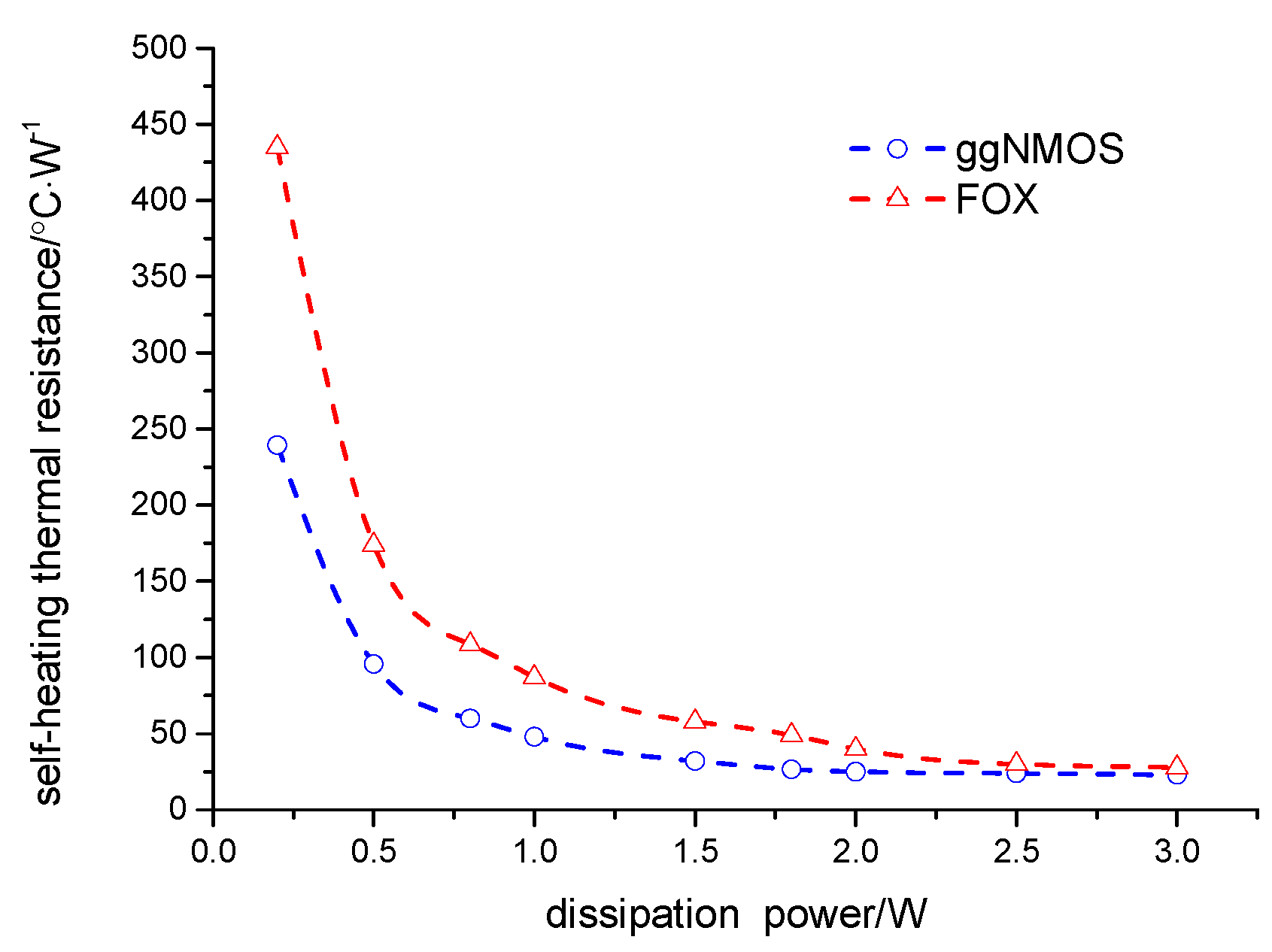
In Figure 8, we can see that the self-heating thermal resistance of the ggNMOS structure protection device exhibits an obvious inverse proportional non-linear relationship with the dissipated power: when the dissipated power is 3W, the self-heating thermal resistance value is 23℃/W; when the dissipated power is 0.25W, the self-heating thermal resistance value is 245℃/W. At the same time, we can see that the self-heating thermal resistance of the FOX structure protection device also exhibits an obvious inverse proportional non-linear relationship with the dissipated power: when the dissipated power is 3W, the self-heating thermal resistance value is 30℃/W; when the dissipated power is 0.25W, the self-heating thermal resistance value is 440℃/W. From the curve data comparison in Figure 8, it can be seen that the relationship curve between the self-heating thermal resistance and the dissipated power of the ggNMOS structure protection device is flatter than that of the FOX structure protection device. As the dissipated power gradually decreases, the change in self-heating thermal resistance of the latter is more drastic than that of the former, which reflects that when the same ESD pulse excitation is applied, the temperature variation range of the ggNMOS structure protection device is smaller than that of the FOX structure protection device, and the former has higher working reliability than the latter.
From the analysis of the experimental data mentioned above, it can be concluded that the self-heating thermal resistance index can universally reflect the temperature distribution characteristics of the ESD event's electro-thermal interaction.
5. Conclusions
This paper presents self-heated thermal resistance as an evaluation indicator of the electrothermal effect of protection devices and provides quantitative relationship expressions of relevant key parameters such as geometric and physical parameters for improving electrothermal properties through the study on the ggNMOS-based ESD protection device. After theoretical analysis and actual tape-out test of both ggNMOS-based protection device and FOX-based protection device, the comparison result shows that when self-heated thermal resistance decreases, the temperature distribution of the protection device tends to be even, the whole temperature decreases and the maximum junction temperature is within the safe operating area, thus improving the reliability of the protection device under a sudden ESD impulse impact.
References
- Steven, H. Voldman. ESD:Physics and Devices.; China Machine Press: Beijing, China, 2014; pp. 57–120. [Google Scholar]
- James Sucec. Heat Transfer.; People’s Education Press: Beijing, China, 1980; pp. 291–327.
- Chen, L.; Zhang, W. R.; Jing, D. Y.; Xie, H. Y. Acta Phys. Sin. 2011, 60, 8501.
- Chen, L. Beijing University of Technology, beijing, 2012.
- Li, M. Z. University of Electronic Science and Technology of China, chengdu, 2007.
- Vladislav A Vashchenko, Andrei Shibkov. ESD Design for Analog Circuits.; Springer Science+Business Media: New York, 2010; p. 87. [Google Scholar]
- Amerasekera, A.; Chang, M.C.; Seitchik, J.; Chatterjee, A.; Mayaram, K.; Chern, J.H. IEEE Transactions on Electron Devices 1993, 1863–1873.
- Amerasekera, A.; Seitchik, J. International Electron Device Meeting (IEDM) Technical Digest, 1994, pp. 446.
- Amerasekera, A.Chapman, R. IEEE Transactions on Electron Devices Letters 1994, 383.
- Walkey, D.; Smy, T.; Reimer, C.; Schroter, M.; Tran, H.; Marchesan, D. Solid State Electronics 2002, 46, 7.
- Wunsch, D. C.; Bell, R. R. IEEE Transactions on Nuclear Science 1968, 15, 6.
- Tasca, D. General Electric Co., 1970, 70, SD401.
- Sozzi, G.; Menozzi, R. Microelectron. Reliab 2007, 27, 65.
- Horng, R. H.; Hong, J. S.; Tsai, Y. L. IEEE T. Electron. Dev 2010, 57, 2203.
- Tsai, M.; Chen, C.; Tsai, W. IEEE T. Compon. Pack. T. 2010, 738.
- Szekely, V. Microelectron. Reliab. 2002, 42, 629.
- Sozzi, G.; Menozzi, R. Microelectron. Reliab. 2007, 27, 65.
- Synopsys Inc. ISE-TCAD Release 8.0 Manuals, 2002.
Figure 1.
Schematic of Active Zone of ggNMOS-based Protection Device

Figure 2.
Change Curve of Self-heated Thermal Resistance vs. Dissipation Power.
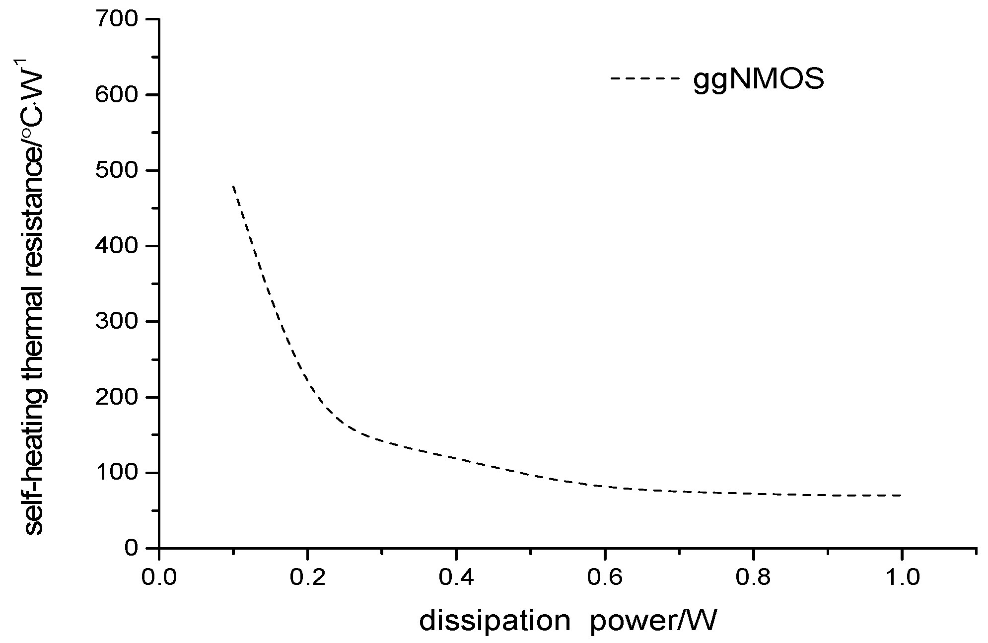
Figure 3.
Temperature Distribution of ggNMOS-based and FOX-based Protection Devices
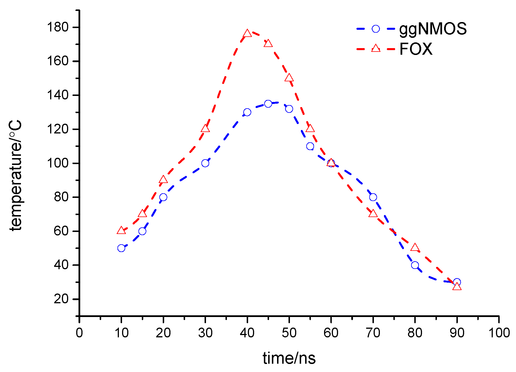
Figure 4.
Simulation Structure Section of ggNMOS-based ESD Protection Device.

Figure 5.
Photo of surface temperature of ESD protection device based on ggNMOS. (The maximum value is 73.87℃, the mean value is 47.05℃ and the minimum value is 24.23℃).
Figure 5.
Photo of surface temperature of ESD protection device based on ggNMOS. (The maximum value is 73.87℃, the mean value is 47.05℃ and the minimum value is 24.23℃).
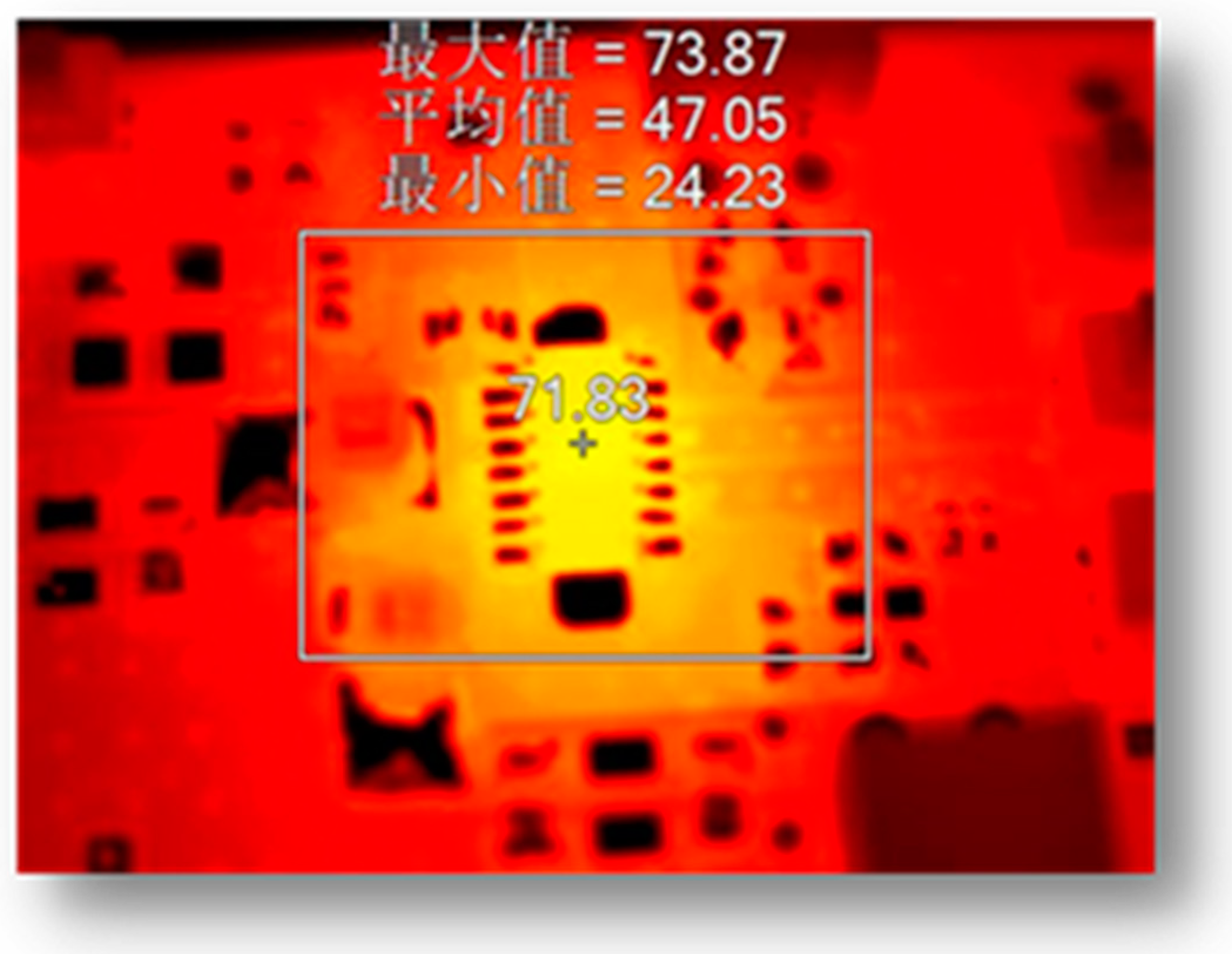
Figure 6.
Photo of surface temperature of ESD protection device based on FOX.(The maximum value is 113.55℃, the mean value is 59.51℃, and the minimum value is 21.40℃).
Figure 6.
Photo of surface temperature of ESD protection device based on FOX.(The maximum value is 113.55℃, the mean value is 59.51℃, and the minimum value is 21.40℃).
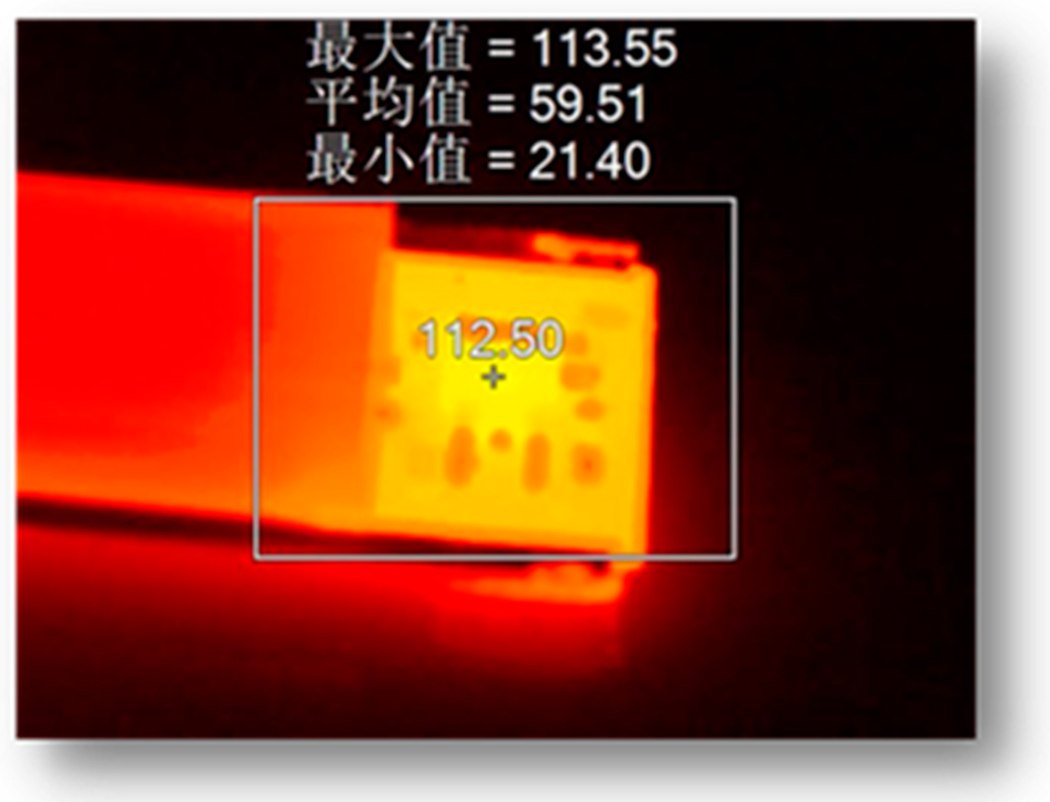
Figure 7.
Measured Variation Curve of Self-heated Thermal Resistance vs. Dissipation Power of ESD Protection Devices (ggNMOS and FOX).
Figure 7.
Measured Variation Curve of Self-heated Thermal Resistance vs. Dissipation Power of ESD Protection Devices (ggNMOS and FOX).
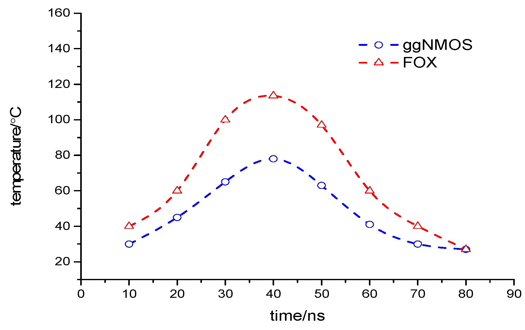
Figure 8.
The curve of ESD protection devices self-heating thermal resistance along with the change of dissipation power(ggNMOS vs FOX).
Figure 8.
The curve of ESD protection devices self-heating thermal resistance along with the change of dissipation power(ggNMOS vs FOX).
Disclaimer/Publisher’s Note: The statements, opinions and data contained in all publications are solely those of the individual author(s) and contributor(s) and not of MDPI and/or the editor(s). MDPI and/or the editor(s) disclaim responsibility for any injury to people or property resulting from any ideas, methods, instructions or products referred to in the content. |
© 2023 by the authors. Licensee MDPI, Basel, Switzerland. This article is an open access article distributed under the terms and conditions of the Creative Commons Attribution (CC BY) license (http://creativecommons.org/licenses/by/4.0/).
Copyright: This open access article is published under a Creative Commons CC BY 4.0 license, which permit the free download, distribution, and reuse, provided that the author and preprint are cited in any reuse.
Submitted:
08 May 2023
Posted:
09 May 2023
You are already at the latest version
Alerts
This version is not peer-reviewed
Submitted:
08 May 2023
Posted:
09 May 2023
You are already at the latest version
Alerts
Abstract
To study the influence of electrothermal effect of ESD protection device on the reliability of inte-grated circuit,a theoretical model of ESD protection device thermal resistance is constructed in the paper based on the Conservation of Energy Principle. By analyzing the temperature relativity between electricity parameter and thermology parameter of ESD protection device characterized by self-heating thermal resistance, the quantitative relationship expression of physical parameter and geometric parameter is obtained, which can be used to improve ESD protection device elec-tro-thermal effect. The simulation testing and the real tape-out testing of ESD protection device self-heating thermal resistance based on ggNMOS are shown and compared. It is concluded that self-heating thermal resistance is an effective index for the protection device electrothermal char-acterization. Based on the established model, the self-heating thermal resistance could be decreased to improve the homogeneity of the heat transference. The uneven distribution of device temperature can be reduced, and the overall reliability of chips can be improved.
Keywords:
Subject: Physical Sciences - Applied Physics
1. Introduction
With the continuous improvement of integrated circuit design technology and production process level, the characteristic size of ESD protection devices is continuously shrinking. The increase in unit area protection device integration inevitably brings about heat dissipation problems, which have increasingly attracted the attention of the integrated circuit industry and related scientific research institutions regarding reliability and thermal failure issues. Therefore, some researchers in academia have shifted the research focus from ESD electrical properties to electric-thermal properties, in-depth research on the physical formation mechanism of protective device electric-thermal effects, proposed methods and measures to reduce and mitigate electric-thermal effects, and hoped to open up a way to solve chip reliability problems from the perspective of ESD electric-thermal properties research. This research idea and method have significant implications for the overall reliability of chips and have practical technological and economic value. As the electrostatic discharge (ESD) [1] protection device is extensively applied on various analog integrated circuit chips [6], RF integrated circuit chips and mixed-signal integrated circuit chips, its thermal stability has become a critical issue. Despite having good electrical properties, ESD protection device generate a rapid rise in lattice temperature [2] when discharging transient high-voltage large-current electrostatic pulses via a single device or device combination. The ESD protection device generates certain heat within a brief time () and limited space ()that causes the electrical parameters of the protected core circuit to drift, which can degrade the rated safe operating range of the core circuit. This may cause the failure of the protected core circuit and lead the occurrence of the irreversible heat dissipation. This mechanism that device temperature rises due to the dissipation power of the ESD protection device is called the electrothermal effect of protection devices. The electrothermal effect has great influence on the ESD protection device and the protected core circuit. This would degrade the normal operation of chips.
In order to study the electrothermal effect of the ESD protection device and also optimize the electrical properties and safe operating area of the core circuit for withstanding external sudden pulse events, people usually adopt thermal resistance as an effective indicator to measure the electrothermal effect of the ESD protection device [7]. Thermal resistance includes ESD self-heated thermal resistance and coupling thermal resistance. Self-heated thermal resistance, mainly determined by the resistance, capacitance and parasitic effect parameters of the protection device, reflects the temperature correlation of the electrical indicators of the ESD protection device and is an effective physical quantity for representing the thermal stability of the ESD protection device. Meanwhile, when the core circuit is operating, power dissipated by its own devices and circuits will also generate certain heat, and the heat generated by the core circuit and the ESD protection device is conducted mutually to cause uneven chip temperature distribution. The thermal resistance for measuring this mutual heat transfer relationship is called coupling thermal resistance.
Due to limitations of technologies and test techniques, the influence of coupling thermal resistance on the electrical parameters of the ESD protection device is ignored here. Along with progress in integrated circuit technologies, the feature size of devices is decreasing constantly, the current density of core circuit is doubled, and SOI technique and dielectric materials are continuously applied to device separation technique, which constantly increase thermal resistance. As a result, the influence of electrothermal effect on chip performance is further intensified. The reliability of the ESD protection device is reduced, and the normal operation of the core circuit is affected. However, because the ESD protection device has diversified structures and poor technological portability currently, there is no general explanation with clear physical significance on relationship between the thermal resistance and electrical parameters and geometric parameters of the ESD protection device.
This paper puts forward a method for calculating the self-heated thermal resistance of ESD protection device based on grounded-gate NMOS (ggNMOS) structure according to the energy conservation law and studies measures for improving the electrothermal effect of ESD protection device. When the core circuit operates normally, a quantitative description is given to correlation among the electrical parameters, geometric parameters and thermal parameters of the ESD protection device by establishing a theoretical model for the thermal resistance of the ESD protection device, and used as an effective reference indicator for increasing the thermal stability of the ESD protection device.
2. Theoretical Model
Figure 1 illustrates the structural diagram of active zone of ggNMOS-based [3] protection device. As the feature size of the device enters deep submicron order, the size of the ESD protection device is very small, and the heating range of the active zone of the device can be equivalent to a parallelepiped [6]. The length, width and height (thickness) of the active zone of the protection device are respectively assumed as b, a and c. The thickness is determined by the technological level of the chip manufacturer and material properties and is usually a fixed constant, so heat source of the active zone of the protection device can be equivalent to a rectangular heat source unit [6]. Because the dimensions of the equivalent rectangular unit are within submicron range, assuming that thermal balance is basically kept between internal and external temperatures of the rectangular unit, the temperature in the center of the rectangular unit can be used for representing the temperature of this active heating region [6].
During normal operating, the ESD protection device is stationary, and the temperature is known T0. When an ESD event occurs, the protection devices suppresses high voltage and discharges high current, heat will be generated inside, and its power is Q0. Meanwhile, partial area As on the outer surface of the ESD protection device is exposed in the chip tube with temperature Tf, the surface coefficient of heat transfer between chip and tube is α, and the object volume of the heat conducting zone of the protection device is V0. The heat generating process inside the ESD protection device follows the energy conservation law:
{Heat entering ESD protection device} + {heat generated by ESD protection device itself} = {Heat discharged from ESD protection device} + {Change of heat stored in ESD protection device}, i.e.:
Hi + Hg = Ho + Hs,
Hi is the heat generated by ESD event, usually a product of voltage and current of human body discharge model (HBM) [10] and a constant Qi; Hg is thermal energy generated by ESD protective device varying with time according to:
Hg = Q0e-βτ,
Ho is the heat transiently transferred by ESD protection device, i.e.:
Ho = αAs(Tj - Tf),
Tj is the internal transient peak temperature of ESD protection device; Hs is the change rate of heat stored in ESD protection device, i.e.:
Substitute the above variables into formula (1) to obtain
Define
ϕ = αAs / mcp,θ = Tj - Tf,
Then formula (5) is transformed into
When intitial conditions: τ = 0, T0 = Tf are substituted into formula (6),
According to JEDEC standard No. 51-1, the self-heated thermal resistance of ESD protection device is defined as
Tj is junction temperature of the device during transient operation, Tf is reference temperature, and PH is power dissipated to the device in the form of heat.
Substitute the above parameters into formula (8) to obtain the final expression of self-heated thermal resistance of ESD protection device:
From the view of energy conservation law, it can be seen that the self-heated thermal resistance of ESD protection device is only related to the thermal conductivity and volume density of device material, heat dissipation surface area and environment temperature, so that various effective physical reference indicators and convenient ways are provided for design optimization of thermal parameters of ESD protection device, and there is obvious guiding significance on thermal stability of whole chip.
3. Results and Discussion
When 0.6 W pulse excitation is input into ESD protection device from outside, the self-heated thermal resistance of ESD protection device can be calculated according to formula (9), as shown in Figure 2 In general, when an ESD event occurs, the protection device is started immediately to suppress injected high voltage within safe operating range, high current enters the chip substrate via a discharge current, generated heat is restricted within the active zone of the device, self-heated thermal resistance is small, and the protective device has good thermal stability. However, when ESD pulse excitation gradually attenuates along with time, the conductivity modulation effect and electrothermal coupling mechanism inside the protection device work, the physical properties of various material layers forming the protection device have microscopic changes to convert partial electric energy into thermal energy, so that the temperature of the protection device rises rapidly, self-heated thermal resistance increases constantly until approaching to irreversible thermal failure state [14]. From Figure 2, it can be seen that when dissipation power is 0.6 W, corresponding self-heated thermal resistance is 79.78℃/W. As dissipation power reduces quickly along with time constant, the electrothermal effect inside the protection device works, partial electric energy is converted into thermal energy, thermal energy cannot be quickly conducted out within a small active heating zone, and the self-heated thermal resistance rises gradually. When dissipation power is attenuated to 0.1 W, corresponding self-heated thermal resistance rises to 478.7℃/W. Hence, the curve of self-heated thermal resistance along with the change of dissipation power of ESD protection device shown in Figure 2 complies with the change relationship between thermal resistance and power consumption in ESD protection device operating principle.
The traditional on-chip ESD protection usually adopts field-oxide (FOX) device [15]. Due to restrictions by the structure and manufacturing technology of this protection device, its self-heated thermal resistance occupies a big space in the central area of the device, and heat cannot be conducted out within short time, so that the temperature in the central area is higher than that at both sides of the device, causing uneven temperature distribution of the whole protection device [16], and that its thermal stability is easily affected by self-heated thermal resistance to decrease. We make a comparison study on ggNMOS-based protection device and FOX-based device to verify the correlation between self-heated thermal resistance and temperature distribution of devices and put forward effective measures for improving thermal stability of protection devices. Figure 3 shows the temperature distribution curves of traditional FOX-based protection device and ggNMOS-based protection device under the same ESD pulse excitation (0.6 W) condition. From the temperature distribution chart, it can be seen that the temperature in the central area of the FOX-based protection device deviates from the temperate at both sides of the protection device by 120℃, while the temperature distribution curve of ggNMOS-based protection device is relatively mild, and the maximum temperature in its central area only deviates from the temperature at both sides of the protection device by 90℃. In addition, the maximum junction temperature of the ggNMOS-based protection device is 135℃, with 41℃ decreased from the maximum junction temperature of the FOX-based protection device. Therefore, from the curves it can be observed that the temperature distribution characteristic of the ggNMOS-based protection device has small amplitude change and becomes mild gradually, self-heated thermal resistance is decreased, and thermal stability is increased.
4. Device Design and Experimental Results
Based on CSMC 0.5 μm 5 V Mixed signal CMOS technology, a two-dimensional physical structure model of the ggNMOS-based device was designed via the draw module in ISE-TCAD [18], and a three-dimensional structure was generated from the two-dimensional device structure via the DIP module [13]. Figure 4 shows the three-dimensional simulation cross-section of the ggNMOS-based device, wherein the channel length is 0.5 μm, the channel width is 60 μm, the distance between surface of contact hole and substrate is 3 μm, the side length of square source-drain contact hole is 0.7 μm, with the drain-gate distance and the gate-source distance respectively set to 10 μm and 5 μm. The geometric parameters and layout of the ggNMOS-based ESD protection device were designed according to the above procedure, and an actual tape-out test has been conducted. For better describing temperature distribution characteristics of the ggNMOS-based device by comparison, the FOX-based device was designed in the same technology and method, which has the same order of magnitude as the ggNMOS-based protection device with regard to the geometric technology parameters as well as dimensions.
We conducted ESD electrical characterization testing of protective devices using the Transmission Line Pulse (TLP) system HANWA HED-T50000. In addition, we performed ESD thermal characterization testing of the chip using a non-contact thermal imager (FLUKE TiX580) and an infrared microscope (FLK-LENS/25MAC2). Initially, we connected the computer, TLP system, digital source meter, and probe station via GPIB bus in accordance with specifications and conventional wiring methods. Then, we placed the protective device on the probe station and connected its electrodes to the probe. The TLP system applied an ESD pulse excitation (rise time of 10ns and pulse width of 100ns) to the protective device through the probe, to measure its static voltage-current characteristics. Based on the voltage-current characteristic test data and curves of the protective device, we determined the state process and state changes of the protective device at several key points. At the same time, we started the thermal imager equipped with the infrared microscope to continuously record the temperature changes of the protective device at several key points, and then processed the recorded temperature data using professional software. Figure 5 and Figure 6 respectively show the real-time photos of the surface temperature distribution of ggNMOS structure protective device and FOX structure protective device under the same ESD pulse excitation conditions, measured using the infrared thermal imager. We extracted the temperature values at each key point during the operation of the ESD protective device from the thermal distribution map using professional software Smartview, and calculated the self-heating thermal resistance, as shown in Figure 7 and Figure 8.
In Figure 7, we observe that when an ESD pulse enters the FOX structure protection device and heats it for 10 ns, the measured surface temperature of the device is 40℃. As the heating time of the ESD pulse increases, the surface temperature of the device gradually decreases, from 98℃ (with a heating time of 50 ns) to 28℃ (with a heating time of 80 ns). At the same time, we also observe that when an ESD pulse enters the ggNMOS structure protection device and heats it for 10 ns, the measured surface temperature of the device is 30℃. when it is increased to 40 ns, the surface temperature reaches its highest value of 73.87℃. The surface temperature of the device then gradually decreases, from 60℃ (with a heating time of 50 ns) to 30℃ (with a heating time of 80 ns). From the data comparison in Figure 7, we can see that the surface temperature distribution of the ggNMOS structure protection device is more uniform than that of the FOX structure protection device. The highest and lowest temperature variations of the former occur within a range of about 50℃, while the latter has a variation range of about 90℃. The temperature function relationship curves of these two protection devices show a normal distribution, which fully characterizes the process of the protection devices experiencing a severe temperature rise, fall, and finally returning to room temperature during ESD events. This temperature change process is in accordance with the physical reality of the protection devices during operation.
In Figure 8, we can see that the self-heating thermal resistance of the ggNMOS structure protection device exhibits an obvious inverse proportional non-linear relationship with the dissipated power: when the dissipated power is 3W, the self-heating thermal resistance value is 23℃/W; when the dissipated power is 0.25W, the self-heating thermal resistance value is 245℃/W. At the same time, we can see that the self-heating thermal resistance of the FOX structure protection device also exhibits an obvious inverse proportional non-linear relationship with the dissipated power: when the dissipated power is 3W, the self-heating thermal resistance value is 30℃/W; when the dissipated power is 0.25W, the self-heating thermal resistance value is 440℃/W. From the curve data comparison in Figure 8, it can be seen that the relationship curve between the self-heating thermal resistance and the dissipated power of the ggNMOS structure protection device is flatter than that of the FOX structure protection device. As the dissipated power gradually decreases, the change in self-heating thermal resistance of the latter is more drastic than that of the former, which reflects that when the same ESD pulse excitation is applied, the temperature variation range of the ggNMOS structure protection device is smaller than that of the FOX structure protection device, and the former has higher working reliability than the latter.
From the analysis of the experimental data mentioned above, it can be concluded that the self-heating thermal resistance index can universally reflect the temperature distribution characteristics of the ESD event's electro-thermal interaction.
5. Conclusions
This paper presents self-heated thermal resistance as an evaluation indicator of the electrothermal effect of protection devices and provides quantitative relationship expressions of relevant key parameters such as geometric and physical parameters for improving electrothermal properties through the study on the ggNMOS-based ESD protection device. After theoretical analysis and actual tape-out test of both ggNMOS-based protection device and FOX-based protection device, the comparison result shows that when self-heated thermal resistance decreases, the temperature distribution of the protection device tends to be even, the whole temperature decreases and the maximum junction temperature is within the safe operating area, thus improving the reliability of the protection device under a sudden ESD impulse impact.
References
- Steven, H. Voldman. ESD:Physics and Devices.; China Machine Press: Beijing, China, 2014; pp. 57–120. [Google Scholar]
- James Sucec. Heat Transfer.; People’s Education Press: Beijing, China, 1980; pp. 291–327.
- Chen, L.; Zhang, W. R.; Jing, D. Y.; Xie, H. Y. Acta Phys. Sin. 2011, 60, 8501.
- Chen, L. Beijing University of Technology, beijing, 2012.
- Li, M. Z. University of Electronic Science and Technology of China, chengdu, 2007.
- Vladislav A Vashchenko, Andrei Shibkov. ESD Design for Analog Circuits.; Springer Science+Business Media: New York, 2010; p. 87. [Google Scholar]
- Amerasekera, A.; Chang, M.C.; Seitchik, J.; Chatterjee, A.; Mayaram, K.; Chern, J.H. IEEE Transactions on Electron Devices 1993, 1863–1873.
- Amerasekera, A.; Seitchik, J. International Electron Device Meeting (IEDM) Technical Digest, 1994, pp. 446.
- Amerasekera, A.Chapman, R. IEEE Transactions on Electron Devices Letters 1994, 383.
- Walkey, D.; Smy, T.; Reimer, C.; Schroter, M.; Tran, H.; Marchesan, D. Solid State Electronics 2002, 46, 7.
- Wunsch, D. C.; Bell, R. R. IEEE Transactions on Nuclear Science 1968, 15, 6.
- Tasca, D. General Electric Co., 1970, 70, SD401.
- Sozzi, G.; Menozzi, R. Microelectron. Reliab 2007, 27, 65.
- Horng, R. H.; Hong, J. S.; Tsai, Y. L. IEEE T. Electron. Dev 2010, 57, 2203.
- Tsai, M.; Chen, C.; Tsai, W. IEEE T. Compon. Pack. T. 2010, 738.
- Szekely, V. Microelectron. Reliab. 2002, 42, 629.
- Sozzi, G.; Menozzi, R. Microelectron. Reliab. 2007, 27, 65.
- Synopsys Inc. ISE-TCAD Release 8.0 Manuals, 2002.
Figure 1.
Schematic of Active Zone of ggNMOS-based Protection Device
Figure 2.
Change Curve of Self-heated Thermal Resistance vs. Dissipation Power.
Figure 3.
Temperature Distribution of ggNMOS-based and FOX-based Protection Devices
Figure 4.
Simulation Structure Section of ggNMOS-based ESD Protection Device.
Figure 5.
Photo of surface temperature of ESD protection device based on ggNMOS. (The maximum value is 73.87℃, the mean value is 47.05℃ and the minimum value is 24.23℃).
Figure 5.
Photo of surface temperature of ESD protection device based on ggNMOS. (The maximum value is 73.87℃, the mean value is 47.05℃ and the minimum value is 24.23℃).
Figure 6.
Photo of surface temperature of ESD protection device based on FOX.(The maximum value is 113.55℃, the mean value is 59.51℃, and the minimum value is 21.40℃).
Figure 6.
Photo of surface temperature of ESD protection device based on FOX.(The maximum value is 113.55℃, the mean value is 59.51℃, and the minimum value is 21.40℃).
Figure 7.
Measured Variation Curve of Self-heated Thermal Resistance vs. Dissipation Power of ESD Protection Devices (ggNMOS and FOX).
Figure 7.
Measured Variation Curve of Self-heated Thermal Resistance vs. Dissipation Power of ESD Protection Devices (ggNMOS and FOX).
Figure 8.
The curve of ESD protection devices self-heating thermal resistance along with the change of dissipation power(ggNMOS vs FOX).
Figure 8.
The curve of ESD protection devices self-heating thermal resistance along with the change of dissipation power(ggNMOS vs FOX).
Disclaimer/Publisher’s Note: The statements, opinions and data contained in all publications are solely those of the individual author(s) and contributor(s) and not of MDPI and/or the editor(s). MDPI and/or the editor(s) disclaim responsibility for any injury to people or property resulting from any ideas, methods, instructions or products referred to in the content. |
© 2023 by the authors. Licensee MDPI, Basel, Switzerland. This article is an open access article distributed under the terms and conditions of the Creative Commons Attribution (CC BY) license (http://creativecommons.org/licenses/by/4.0/).
Copyright: This open access article is published under a Creative Commons CC BY 4.0 license, which permit the free download, distribution, and reuse, provided that the author and preprint are cited in any reuse.
The Influence of Non-Uniform High Heat Flux on Thermal Stress of Thermoelectric Power Generator
Tingzhen Ming
et al.
Energies,
2015


MDPI Initiatives
Important Links
© 2024 MDPI (Basel, Switzerland) unless otherwise stated