1. Introduction
Photoluminescence (PL) is one of the most important optical processes, underlying relaxation of two-level quasi-molecular systems upon their complementary optical excitation [
1]. Even single PL photons could be acquired and spatially resolved much easier than differential absorption of single photons. As a result, PL characterization in 2D- or 3D-scanning confocal micro- or nano-spectroscopy mode became an enabling tool for probing local molecular or crystalline structures [
2,
3], or electromagnetic near-fields [
4,
5].
(Sub)microscale laser modification of molecular or crystalline structures and related PL spectra underlies facile and robust encoding of bulk diamonds for their tracing applications in identifying synthetic diamonds between natural ones in large commercial diamond collections [
6], protecting trademarks of high-quality natural (potentially, synthetic too) diamond manufacturers [
7], limiting commercial trading and marketing of illegal diamonds. This PL-based encoding appears unique in diamonds, where other popular encoding technologies – ablation fabrication of (sub)microscale voids [
8] or birefringent nanogratings [
9,
10] – don’t work in the ultra-hard diamond lattice, better tending to graphitization [
11], while PL read-out is more simple and sensitive. Similarly, many other crystalline scintillators and luminophores undergo laser modification of their crystalline structures and related PL spectra [12-14], potentially promising for optical encoding (writing/read-out) applications in storage devices.
In this work we report an evaluation study of natural diamond, LiF and CaF2 crystals as optical platforms for microscale photoluminescent encoding by ultrashort-pulse lasers for archival optical storage, their tests of potential capacity and viability.
2. Materials and Methods
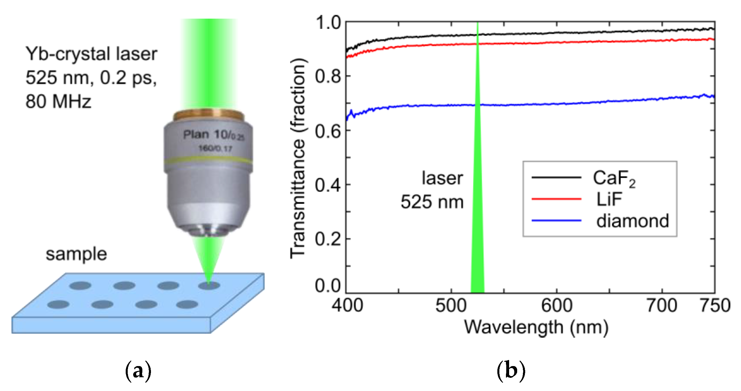
In these studies, a 2-mm thick colorless brick of IaA-type natural diamond (total concentration of nitrogen atoms ≈130 ppm), and 5-mm thick slabs of undoped LiF and CaF
2 crystals grown by Bridgman-Stockbarger method were utilized, being optically transparent at the writing laser wavelength of 525 nm (
Figure 1a). The samples were characterized in the spectral range of 350–750 nm by room-temperature (RT) optical transmission microspectroscopy (
Figure 1b), using an ultraviolet(UV)−near-IR microscope-spectrometer MFUK (LOMO, Saint-Petersburg, Russia). Inscription inside these bulk crystals at the depth of 100 μm (fluorides) and of 120 μm (diamond) in their transparency spectral region (
Figure 1b), accounting for their 525-nm refractive indexes of 2.4 (diamond), 1.4 (LiF) and 1.4 (CaF
2) [
15], was performed by second-harmonic (525 nm) pulses of the Yb-crystal laser TEMA (Avesta Project, Moscow, Russia) with the pulsewidth (full width at a half maximum) of 0.2 ps, repetition rate of 80 MHz cut in pulse bunches of 0.05÷10-s duration by a mechanical shutter, and 50-nJ (average power – 4 W) maximum output pulse energy E in the TEM
00 mode. The 525-nm laser pulses with variable energies E ≤ 50 nJ were focused in a sub-filamentary regime (filamentation threshold energy ≈ 300 nJ (diamond), 260 nJ (CaF
2) [
16]) by a 0.65-NA micro-objective into ≈1-μm wide spots (1/e-intensity diameter) inside the crystals, providing the peak laser fluence <6 J/cm
2 and peak laser intensity <30 TW/cm
2. The samples were mounted on a computer-driven three-dimensional motorized translation stage and exposed in separate position with variable transverse spacings in the range of 1-5 microns and longitudinal spacings in the range of 1–28 microns.
Annealing of fluoride samples was performed at different temperatures in the range of 25–300°C (20-min temperature ramp, 30 min – stationary heating), using a temperature-controlled mount for Raman micro-spectroscopy, while the diamond sample was annealed in an evacuated oven during 1 hour at different temperatures in the range of 25–1200°C.
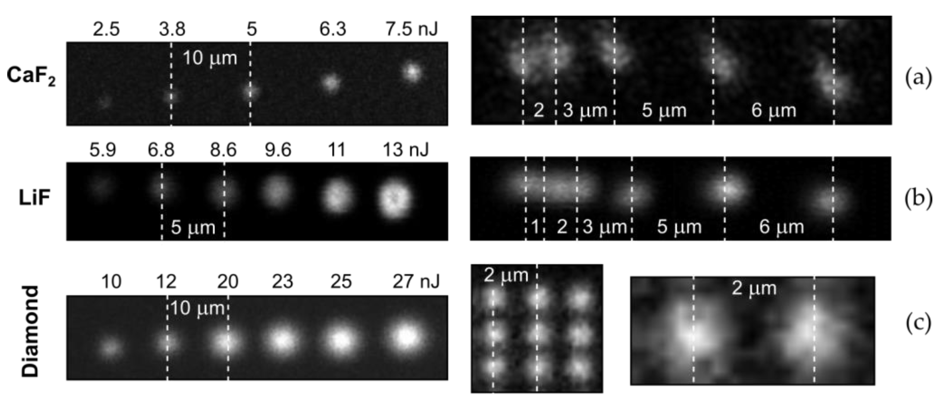
In our characterization studies, top-view and side-view (cross-sectional) photoluminescence imaging at the 532-nm pump cw-laser wavelength and magnification 100x (NA = 1.45, spatial resolution ~1 μm) was performed by means of a 3D-scanning confocal photoluminescence/Raman microscope Confotec MR520 (SOL Instruments, Minsk, Belarus) to measure relative intensity, spatial dimensions and optical PL-acquired separation of PL microbits (
Figure 2).
3. Experimental Results and Discussion
3.1. Inscription of Photo-Luminescent Microbits
PL microbits were inscribed in the bulk crystalline CaF
2 and LiF slabs, as well as in the diamond plate, at different pulse energies (
Figure 2a-c, left side). Specifically, the PL microbits inside the CaF
2 slab exhibit the corresponding energy-dependent microbit dimensions above the inscription threshold value ≈3 nJ at the exposure of 10
7--10
9 pulses/microbit. Similarly, the PL microbits were inscribed inside the LiF slab in the same energy range, while the threshold energy appears considerably higher (≈ 5 nJ,
Figure 2b, left side) at the exposure of 10
7--10
9 pulses/microbit, reflecting the higher bandgap energy of 13.0-14.2 eV in LiF [
17,
18], comparing to CaF
2 –11.5-11.8 eV [
19,
20]. Finally, in the diamond plate the PL microbits were inscribed as a function of laser pulse energy, demonstrating their increasing dimensions at the exposure of 10
7--10
9 pulses/microbit (
Figure 2c, left side). Surprisingly, against our expectations, the inscribed microbits appear inhomogeneous at higher magnifications (
Figure 2a-c, right side) because of well-known high degree of clustering – up to nanoscale - for fluorine atoms around dislocations in the fluoride crystals [
21], while in diamonds such segregation of vacancies and interstitials also occurs in the form of multi-vacancies (voidities) [
22] or interstitial aggregates in B2-centers [
22]. In the same line, these microbits look diffuse owing to the low diffusion energies ~ 0.1 eV of interstitials and vacancies [
21], facilitating room-temperature internal segregation and external collateral spreading of point-defect concentrations in the PL microbits.
In terms of spatial resolution of the PL microbits during the laser inscription process, even at low above-threshold pulse energies these features could be more or less resolved only at their 2-μm separation (
Figure 2a-c, right side). The main reason of such moderate lateral (transverse) resolution is apparently the initial focal 1/e-diameter of 1 μm at the focusing NA = 0.65 (see
Section 2 – Materials and Methods), additionally increased by ≈1-μm lateral diffusion length of fs-laser generated electron-hole plasma during its electron-lattice thermalization over the 1-2 picoseconds [
23]. The corresponding point beam stability upon the focusing could result in negligible lateral displacements ~10 nm. As a result, distinct resolution of the neighboring PL microbits becomes possible for their lateral separations, exceeding 2-μm distance. Meanwhile, it could be considerably improved till ~1-1.5 μm, utilizing specially designed high-NA (0.75-0.9) air focusing micro-objectives. Below, in
Section 3.4 the longitudinal (interlayer) spatial resolution will be tested in the case of brightly luminescent LiF crystal to evaluate the potential optical storage capacity of PL microbit arrays.
3.2. Photo-Luminescence Spectra of Microbits: Atomistic Inscription and Annealing Mechanisms
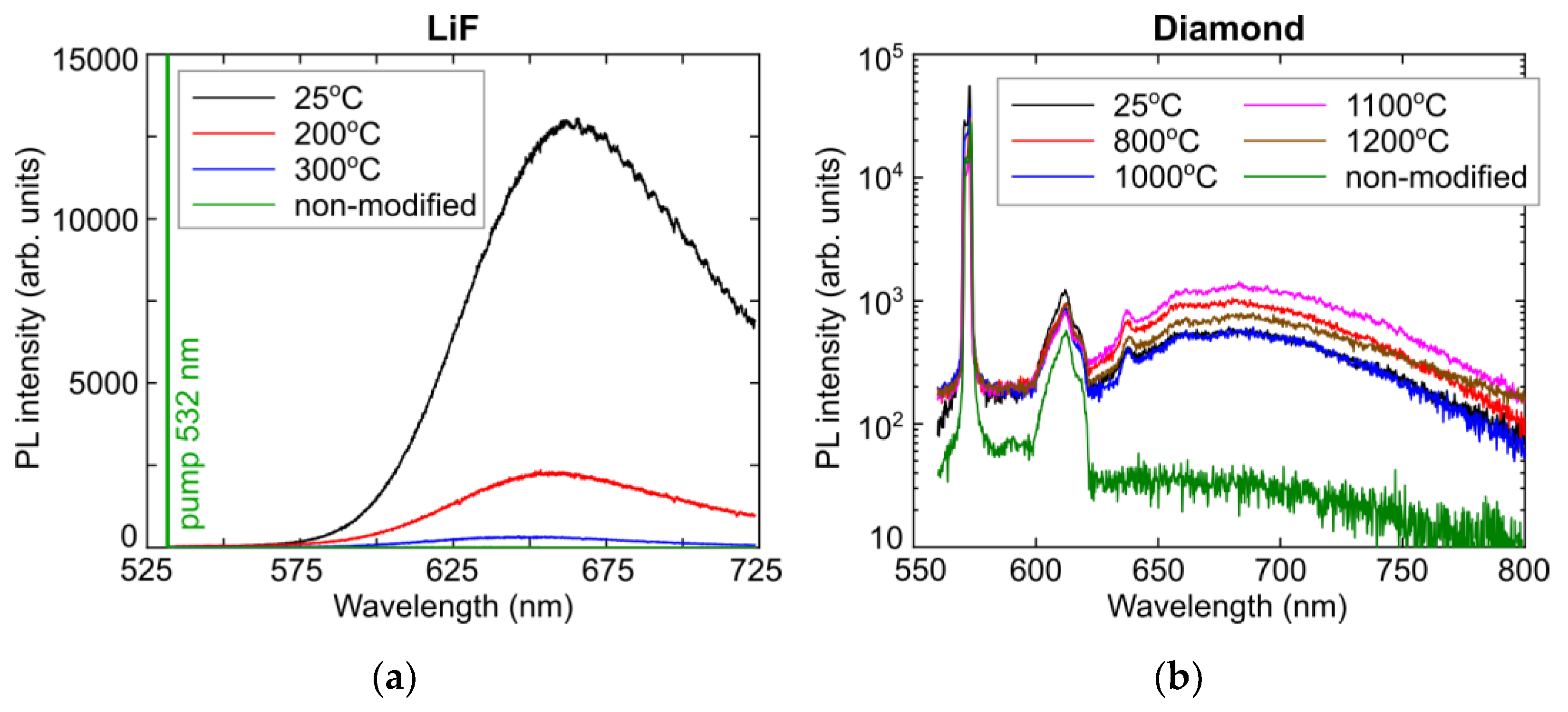
Typical PL spectra acquired in the laser-inscribed microbits by 3D-scanning confocal PL micro-spectroscopy are presented in
Figure 3 in comparison to the corresponding spectra of the background non-modified materials. Specifically, the CaF
2 slab exhibits the strongly enhanced PL yield in the region of 650-850 nm, peaked at 740 nm (
Figure 3a). Though PL spectra of electronic excitations in fluorides are rather flexible due to high mobility of Frenkel defects and the multitude of their complexes [21,24-25], the observed peak could be assigned to some of these vacancy aggregates (F
x0,+, where F is the fluorine vacancy with the rapped electron, x > 2 and upper indexes “
0,+” denote the charged states). Similarly, in the LiF slab the increased PL band in the range of 550-750 nm could be assigned to F
2 (peak at 670 nm [
24]) and F
3 (peak at 650 nm [
24]) centers, while the emerging PL band with its peak at 800-850 nm could also related to some unknown yet F
x0,+ centers [21,24-25].
Finally, the observed strongly – by one order of magnitude - enhanced PL band in the micromark inscribed inside the diamond slab exhibits the main spectral features, representing the neutral (NV
0, zero-phonon line, ZPL, at 575 nm [
22]) and negatively charged nitrogen-vacancy (NV
−, zero-phonon line at 637 nm [
22]) centers of a substitutional nitrogen atoms with a photo-generated vacancy, as well as their red-shifted phonon replica.
Atomistic processes underlying the observed laser-induced transformations of PL spectra in LiF and CaF
2 are supposed to be associated with aggregation of mobile neutral (I-center [
21]) and negatively charged (F-center [
21]) vacancies, along with fluorine neutral (H-center [
21]) and negatively charged (α-centers [
21]) interstitials (Eq. 1a), approaching to hundreds of aggregated defects usually concentrated in dislocation loops [
21]. Likewise, in the diamond plate the mobile photo-generated vacancies could be trapped by substitutional nitrogen atoms (C-centers [
22]), resulting in well-known neutral or charged NV complexes [
12,
22] (Equation (1b)):
Equation (1). Atomistic processes, resulting in photo-induced vacancy complexes in fluorides and diamond.
In the same line, one can see strong stationary annealing of mobile vacancy-related color centers in LiF already at temperatures, elevated by 200-300°C (
Figure 4a), almost deleting the microbit signal. In contrast, in denser and more rigid diamond lattice the Frenkel vacancies anchored by C-centers, remain rather stable even at high temperatures, approaching to 1200°C (
Figure 4b).
3.3. Photogeneration of Frenkel Pairs of Point Defects in LiF during Atomistic Inscription
PL yield at 670 nm – in the peak related to F
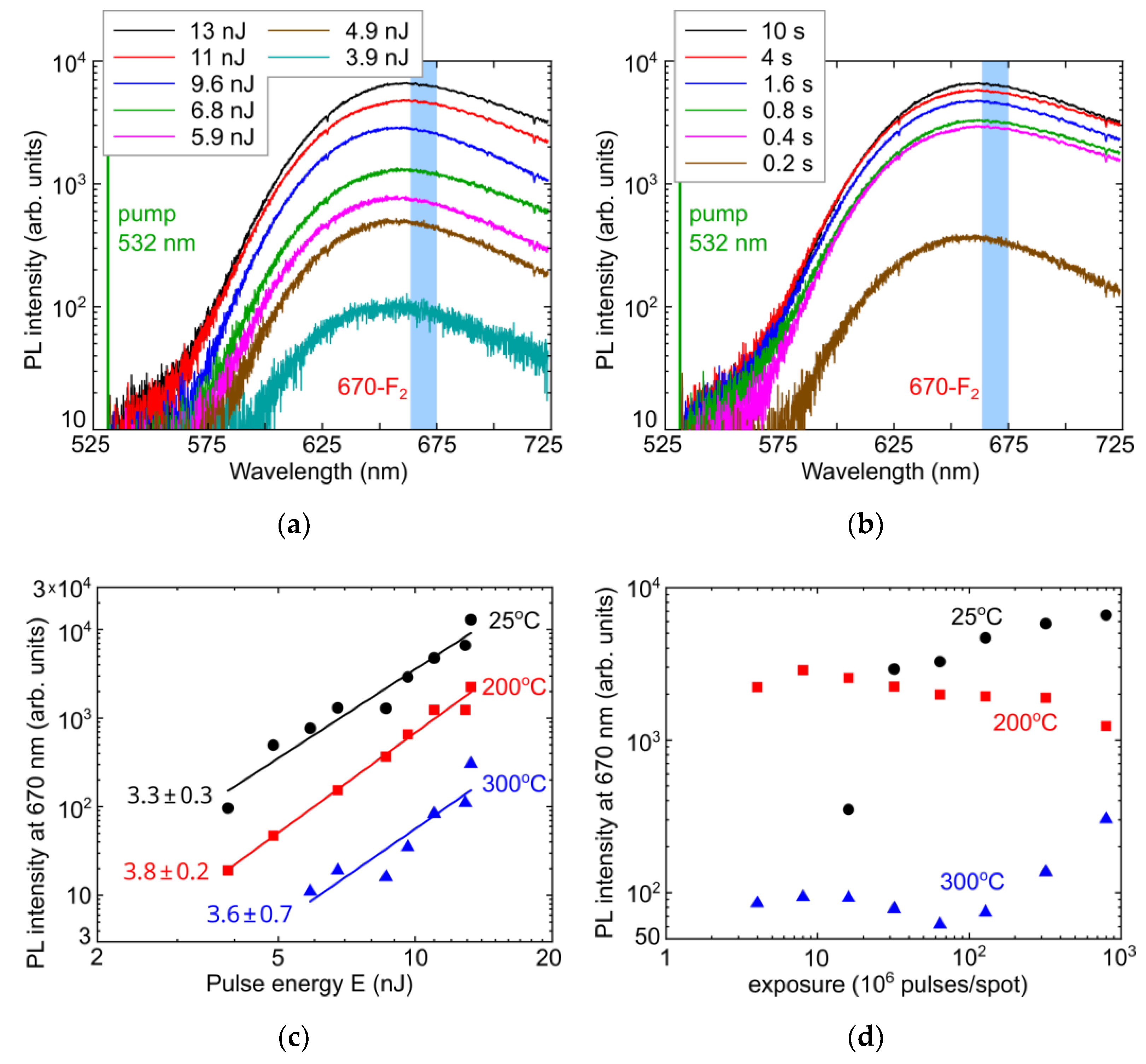
2-centers – was used to track fs-laser photogeneration of Frenkel pairs in LiF, underlying the formation of these centers. As can be seen in
Figure 5a,c, the PL yield in LiF exhibits the non-linear (power slope in the range of ≈ 3.3-3.8) monotonic dependence on pulse energy E = 2.5-13 nJ (peak fluence ≈ 0.3-1.7 J/cm
2, peak intensity ≈ 1.5-9 TW/cm
2) (previously – in diamond [
26]) and exposure of (4-800)×10
6 pulses/spot (at room temperature,
Figure 5b,d). Moreover, the abovementioned annealing effect at the temperatures of 200°C and 300°C results not only in the decreased PL intensity at 670 nm (
Figure 5c), but also in the different exposure trends (
Figure 5d) apparently related to cumulative heating of the material at the ultra-high 80-MHz exposure of the static sample, which is well-known to be favorable for self-trapped exciton stabilization via Frenkel pair formation [
21]. The cumulative heating effect is more pronounced at the room temperature (
Figure 5d), while the elevated temperatures make it less distinct.
We have analyzed the observed PL yield at 670 nm vs pulse energy E in LiF (
Figure 5c), representing the concentration of F
2-centers in the probed confocal volume, alike to our previous similar studies in diamond [
26]. According to high bandgap energy of E
dir(Г-point) ≈ 13.0-14.2 eV in LiF [
17,
18], formation of F
2-centers requires either N = E
dir/ħω ≈ 6 photons at the 525 nm wavelength (photon energy ħω ≈ 2.4 eV), or “hot” non-equilibrium electron of this energy (effectively, considerably higher to fulfill both the quasi-momentum and energy conservation laws). The evaluated laser-induced prompt ponderomotive enhancement of the bandgap [
27,
28], U
p =e
2E
2/(4m
optω
2), is minor (<1 eV) in the utilized intensity range of 9-30 TW/cm
2 (electric field strenth E=15-30 MV/cm) for the arbitrary optical mass of electron-hole pair m
opt = m
em
h/(m
e+m
h) = m
0/2, assuming m
e,m
h = m
0 (free-electron mass).
Recently, for such analysis of electron-hole plasma and PL dynamics a kinetic rate model for electron-hole plasma density ρ
eh was enlighteningly used in the common form [
29], including 1) ultrafast, pulsewidth-limited multiphoton (cross-section σ
N) and 2) impact ionization (coefficient α), 3) fast picosecond Auger (coefficient γ) and 4) slow radiative (coefficient β) recombination, as well as 5) fast self-trapping of electron-hole pairs (excitons, characteristic time τ
str) to produce one color center per self-trapped excitons [
21] as the consecutive terms, respectively, and describing the corresponding continuous-wave-laser pumped PL yield Φ
PL as follows (Eq. 2a) [
23]:
Equation 2. Kinetic rate equations for electron-hole plasma and related PL yield Φ
PL of the F
2-centers produced via exciton self-trapping [
21]: (a) general form, (b) case-specific form for our experiments in LiF.
In the case of LiF, Equation 2a could be presented in the case - specific form (Eq. 2b), where the only six-photon ionization and Auger recombination balance each other, while excitonic self-trapping accompanies the electron-hole plasma relaxation. As a result, PL yield could follow the non-linear dependence on I
0 with the power slope ≈ 4, being consistent with the measured values of 3.3-3.8 (
Figure 5c).
3.4. Evaluation of Storage Capacity of Photo-Luminescent Microbits
Finally, we have performed experimental evaluation of PL microbit density, which is the key characteristic of archival optical storage. Above, we have inscribed PL bits in the natural diamond, LIF and CaF
2 samples with ≥2-μm lateral separation, which could be easily resolved in PL images (
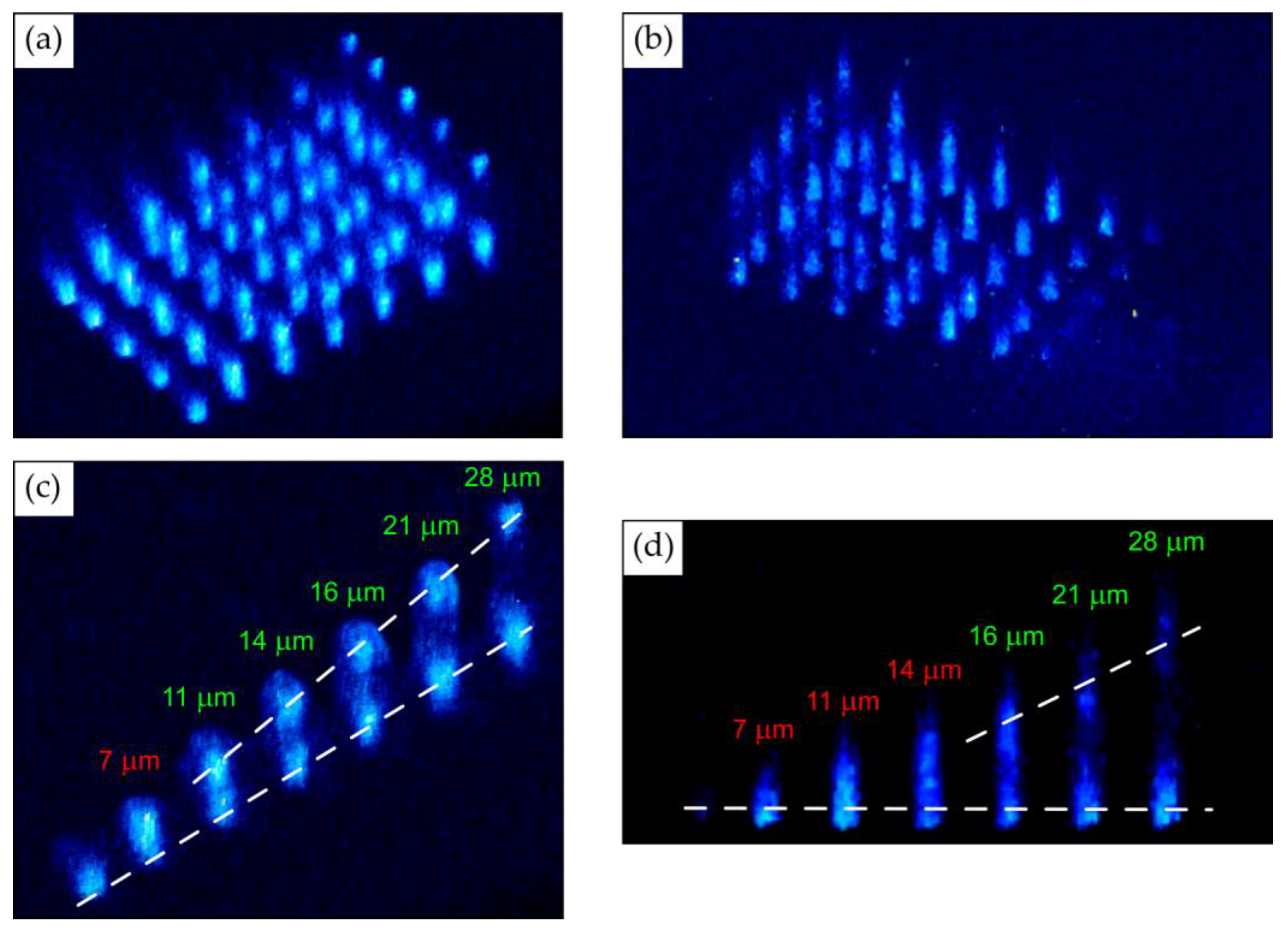
Figure 2). Furthermore, we have undertaken inscription and confocal PL visualization of separate linear arrays of PL microbits with variable vertical (depth) separation, changing in the range of 1-28 μm (
Figure 6), in order to evaluate the minimal resolvable vertical separation. PL visualization was performed by means of Olympus (40x) and Nikon (100x) microscope objectives with vertical resolution Δz = 1 or 2 μm, respectively (
Figure 6a,b). The corresponding side-view PL imaging results for the same microstructure of paired linear arrays are presented in
Figure 6c,d.
Here, one can find that the pairs of the microbit lines become visibly separable, staring from 11 μm for the 1μm-resolution visualization (
Figure 6c), while only at 16 or 21 μm – for the 2μm-resolution visualization (
Figure 6d). Hence, accounting for the appropriately resolvable 2-μm intra-layer separation of microbits and their 11-μm inter-layer separation, one can evaluate for the simple cubic lattice of microbits the bulk microbit density of 25 Gbits per cubic centimeter, i.e., about 3 Tbits per disk for the 120-mm diameter of the standard CV or DVD disks and the 10-mm thickness. This optical storage capacity is comparable to previous optical memory writing technologies (visible microvoids [
8], birefringent nanotrenches [
9,
10], photoluminescent microbits [
30]), but have clear benefits in the confocal non-linear memory read-out due to non-destructive laser inscription technology. Moreover, considerable, few-fold additional increase in the storage capacity could be achieved by higher-NA (NA > 0.65) inscription and other advanced optical means.
4. Conclusions
In this study, bulk high-NA inscription (writing) of photo-luminescent microbits in LiF, CaF2 and diamond crystals was performed by means of ultrashort-pulse laser and tested (read-out) by 3D-scanning confocal photoluminescence micro-spectroscopy. Preliminarily, optical storage density for the simple cubic lattice of microbits was evaluated as high as 25 Gbits/cm3, but could be few-fold increased by using more sophisticated optical focusing tools. Photo-luminescent color centers were identified in the fluorides (fluorine vacancy-based F2-centers) and diamond (carbon vacancy-based NV-centers) by the PL micro-spectroscopy, while their laser inscription mechanism was revealed in fluorides for the first time, comparing to the know mechanism for synthetic diamonds. Moreover, the color centers could be easily annealed in the fluorides at moderate temperatures of 300°C due to the high lability of the centers and room-temperature mobility of their atomistic constituents, comparing to the relatively robust color (NV) centers in the diamond, persisting even at rather elevated temperatures ≈1200°C. Our research paves the way for potential implications of laser-inscribed photo-luminescent microbits in archival optical storage.
Author Contributions
Conceptualization, S.K., P.D. and A.G.; methodology, I.M.; validation, E.K.; investigation, A.R., P.D., N.S. and E.K.; resources, A.R., G.K. and R.K.; writing—original draft preparation, S.K.; writing—review and editing, A.G. and S.K.; visualization, P.D., E.K. and N.S.; supervision, A.G.; project administration, S.K.; and funding acquisition, S.K. All authors have read and agreed to the published version of the manuscript.
Funding
This research was funded by the Russian Science Foundation (project no. 21-79-30063); https://rscf.ru/en/project/21-79-30063/.
Data Availability Statement
The data supporting the reported results are presented in part in Supplementary data and can be also obtained from the authors.
Conflicts of Interest
The authors declare no conflict of interest.
References
- Levshin, L.; Saletskii, A. Optical Methods for Studying Molecular Systems. Molecular Spectroscopy; MGU: Moscow, Russia, 1994. [Google Scholar]
- Yang, B.; Chen, G.; Ghafoor, A.; Zhang, Y.; Zhang, Y.; Zhang, Y.; Hou, J.G. Sub-nanometre resolution in single-molecule photoluminescence imaging. Nature Photonics 2020, 14, 693–699. [Google Scholar] [CrossRef]
- Goldschmidt, J. C.; Fischer, S. Upconversion for photovoltaics–a review of materials, devices and concepts for performance enhancement. Advanced Optical Materials 2015, 3, 510–535. [Google Scholar] [CrossRef]
- Kudryashov, S.I.; Danilov, P.A.; Porfirev, A.P.; Saraeva, I.N.; Kuchmizhak, A.A.; Rudenko, A. A.; Busleev, N.I.; Umanskaya, S.F.; Zayarny, D.A.; Ionin, A.A.; Khonina, S.N. Symmetry-wise nanopatterning and plasmonic excitation of gold nanostructures by structured femtosecond laser pulses. Optics Letters 2019, 44, 1129–1132. [Google Scholar] [CrossRef] [PubMed]
- Zhizhchenko, A. Y.; Tonkaev, P.; Gets, D.; Larin, A.; Zuev, D.; Starikov, S. . Makarov, S. V. Light-emitting nanophotonic designs enabled by ultrafast laser processing of halide perovskites. Small 2020, 16, 2000410. [Google Scholar] [CrossRef] [PubMed]
- Tsai, T. H. Imaging-assisted Raman and photoluminescence spectroscopy for diamond jewelry identification and evaluation. Applied Optics 2023, 62, 2587–2594. [Google Scholar] [CrossRef] [PubMed]
- ALROSA. Identification of diamonds using laser nanomarks. Available online: https://youtu.be/X3Z_jcWowks (accessed on 11 December 2022).
- Hong, M. H.; Luk’yanchuk, B.; Huang, S. M.; Ong, T. S.; Van, L. H.; Chong, T. C. Femtosecond laser application for high capacity optical data storage. Applied Physics A 2004, 79, 791–794. [Google Scholar] [CrossRef]
- Wang, H.; Lei, Y.; Wang, L.; Sakakura, M.; Yu, Y.; Shayeganrad, G.; Kazansky, P.G. 100-Layer Error-Free 5D Optical Data Storage by Ultrafast Laser Nanostructuring in Glass. Laser & Photonics Reviews 2022, 16, 2100563. [Google Scholar]
- Lipatiev, A.S.; Fedotov, S.S.; Lotarev, S.V.; Lipateva, T.O.; Shakhgildyan, G.Y.; Sigaev, V.N. Single-Pulse Laser-Induced Ag Nanoclustering in Silver-Doped Glass for High-Density 3D-Rewritable Optical Data Storage. ACS Applied Nano Materials 2022, 5, 6750–6756. [Google Scholar] [CrossRef]
- Ionin, A.A.; Kudryashov, S.I.; Mikhin, K.E.; Seleznev, L.V.; Sinitsyn, D.V. Bulk femtosecond laser marking of natural diamonds. Laser Phys. 2010, 20, 1778–1782. [Google Scholar] [CrossRef]
- Chen, Y.C.; Salter, P.S.; Knauer, S.; Weng, L.; Frangeskou, A.C.; Stephen, C.J.; Ishmael, S.N.; Dolan, P.R.; Johnson, S.; Green, B.L.; Morley, G.W.; Newton, M.E.; Rarity, J.G.; Booth, M.J.; Smith, J.M. Laser writing of coherent colour centres in diamond. Nat. Photonics 2017, 11, 77–80. [Google Scholar] [CrossRef]
- Chekalin, S. V.; Kompanets, V. O.; Dormidonov, A. E.; Kandidov, V. P. Influence of induced colour centres on the frequency–angular spectrum of a light bullet of mid-IR radiation in lithium fluoride. Quantum Electronics 2017, 47, 259. [Google Scholar] [CrossRef]
- Castelletto, S.; Maksimovic, J.; Katkus, T.; Ohshima, T.; Johnson, B.C.; Juodkazis, S. Color centers enabled by direct femtosecond laser writing in wide bandgap semiconductors. Nanomaterials 2020, 11, 72. [Google Scholar] [CrossRef] [PubMed]
- Palik, E.D. Handbook of Optical Constants of Solids; Academic Press: Orlando, USA, 1998. [Google Scholar]
- Kudryashov, S. I.; Danilov, P. A.; Kuzmin, E. V.; Gulina, Y. S.; Rupasov, A. E.; Krasin, G. K. . Ionin, A. A. Pulse-width-dependent critical power for self-focusing of ultrashort laser pulses in bulk dielectrics. Optics Letters 2022, 47, 3487–3490. [Google Scholar] [CrossRef] [PubMed]
- Samarin, S.; Artamonov, O. M.; Suvorova, A. A.; Sergeant, A. D.; Williams, J. F. Measurements of insulator band parameters using combination of single-electron and two-electron spectroscopy. Solid state communications 2004, 129, 389–393. [Google Scholar] [CrossRef]
- Karsai, F.; Tiwald, P.; Laskowski, R.; Tran, F.; Koller, D.; Gräfe, S.; Blaha, P. F center in lithium fluoride revisited: Comparison of solid-state physics and quantum-chemistry approaches. Physical Review B 2014, 89, 125429. [Google Scholar] [CrossRef]
- Ma, Y.; Rohlfing, M. Quasiparticle band structure and optical spectrum of CaF2. Physical Review B 2007, 75, 205114. [Google Scholar] [CrossRef]
- Chen, J.; Zhang, Z.; Guo, Y.; Robertson, J. Electronic properties of CaF2 bulk and interfaces. Journal of Applied Physics 2022, 131, 215302. [Google Scholar] [CrossRef]
- Song, K.; Williams, R.T. Self-trapped excitons; Springer-Verlag Berlin: Heidelberg, Germany, 1993. [Google Scholar]
- Zaitsev, A. M. Optical properties of diamond: a data handbook. Springer-Verlag Berlin: Heidelberg, Germany, 2001. [Google Scholar]
- Kudryashov, S.; Danilov, P.; Smirnov, N.; Krasin, G.; Khmelnitskii, R.; Kovalchuk, O. . Levchenko, A. “Stealth Scripts”: Ultrashort Pulse Laser Luminescent Microscale Encoding of Bulk Diamonds via Ultrafast Multi-Scale Atomistic Structural Transformations. Nanomaterials 2023, 13, 192. [Google Scholar] [CrossRef]
- Lakshmanan, A. R.; Madhusoodanan, U.; Natarajan, A.; Panigrahi, B. S. Photoluminescence of F-aggregate centers in thermal neutron irradiated LiF TLD-100 single crystals. Physica status solidi (a) 1996, 153, 265–273. [Google Scholar] [CrossRef]
- Davidson, A. T.; Kozakiewicz, A. G.; Comins, J. D. Photoluminescence and the thermal stability of color centers in γ-irradiated LiF and LiF (Mg). Journal of applied physics 1997, 82, 3722–3729. [Google Scholar] [CrossRef]
- Kudryashov, S.I.; Danilov, P.A.; Smirnov, N.A.; Stsepuro, N.G.; Rupasov, A.E.; Khmelnitskii, R.A.; Oleynichuk, E.A.; Kuzmin, E.V.; Levchenko, A.O.; Gulina, Y.S.; Shelygina, S.N.; Sozaev, I.V.; Kovalev, M.S.; Kovalchuk, O.E. Signatures of ultrafast electronic and atomistic dynamics in bulk photoluminescence of CVD and natural diamonds excited by ultrashort laser pulses of variable pulsewidth. Appl. Surf. Sci. 2021, 575, 151736. [Google Scholar] [CrossRef]
- Keldysh, L.V. Ionization in the field of a strong electromagnetic wave. Sov. Phys. JETP 1965, 20, 1307–1314. [Google Scholar]
- Kudryashov, S.I. Microscopic model of electronic Kerr effect in strong electric fields of intense femtosecond laser pulses. In Proceedings of the Conference on Quantum Electronics and Laser Science, Baltimore, Maryland, USA, May 2005. JThE26. [Google Scholar]
- Bulgakova, N.M.; Stoian, R.; Rosenfeld, A.; Hertel, I.V.; Campbell, E.E.B. Electronic transport and consequences for material removal in ultrafast pulsed laser ablation of materials. Phys. Rev. B 2004, 69, 054102. [Google Scholar] [CrossRef]
- Ren, Y.; Li, Y.; Guo, K.; Cui, Z.; Wang, C.; Tan, Y. . Cai, Y. Dual-modulation of micro-photoluminescence in rare-earth-doped crystals by femtosecond laser irradiation for 5D optical data storage. Optics and Lasers in Engineering 2023, 167, 107612. [Google Scholar] [CrossRef]
|
Disclaimer/Publisher’s Note: The statements, opinions and data contained in all publications are solely those of the individual author(s) and contributor(s) and not of MDPI and/or the editor(s). MDPI and/or the editor(s) disclaim responsibility for any injury to people or property resulting from any ideas, methods, instructions or products referred to in the content. |
© 2023 by the authors. Licensee MDPI, Basel, Switzerland. This article is an open access article distributed under the terms and conditions of the Creative Commons Attribution (CC BY) license (http://creativecommons.org/licenses/by/4.0/).
