Preprint
Article

Research on Heat transfer and IR Characteristics of Molybdenum Sputtered Polyamide Materials

Altmetrics

Downloads

151

Views

99

Comments

0

A peer-reviewed article of this preprint also exists.

This version is not peer-reviewed

Submitted:

12 May 2023

Posted:

15 May 2023

You are already at the latest version

Alerts
Abstract
Demand for development of the convergence industry, research studies on electrical conductivity, thermal characteristics, semiconductors, motors, and batteries using special materials have come to the fore. Meanwhile, molybdenum (Mo) exhibits relatively small inorganic qualities, and the thermal conductivity rate is applied to various fields. In this study, in-depth characteristics were considered regarding the concentration of thermal characteristics, IR car terminal characteristics, and IR ve-hicles. This study calculated each phase temperature of the molybdenum sputtered specimens in the steady state according to the heat transfer theory. When the molybdenum-sputtered fabric’s metal layer pointed to the outside air, the heat transfer rate (Q) was high at 5748.3W, In contrast, if the molybdenum sputtered film’s metal layer of the pointed toward the heat source, the heat transfer rate (Q) was low at 187.1W. As a result of measuring the IR transmittance, the infrared transmit-tance of the molybdenum sputtering-treated sample was significantly reduced compared to the untreated sample. In the case of untreated samples, the transmittance ranged from 92.7 to 42.0%. When only the cross part was treated with molybdenum sputtering and the molybdenum surface was directed toward the IR irradiator, the IR transmittance was 66.8~0.7%. It is believed that the molybdenum sputtering polyamide samples produced in this study can be applied to multifunc-tional military wear, biosignal detection sensors, semiconductor products, batteries, etc., by utilizing excellent electrical properties, stealth functions, IR blocking properties, and lightness for infrared thermal imaging detectors.
Keywords: 
Subject: Chemistry and Materials Science  -   Materials Science and Technology

1. Introduction

Molybdenum (Mo) is a relatively non-toxic inorganic substance that not only provides hard and non-corrosive steel even at high temperatures but also is used as a nutritional supplement to living organisms. Molybdenum is mechanically strong from cryogenic to high temperature, has a high elasticity, has thermal conductivity that is several times higher than that of a general heat-resistant alloy, and has a small linear expansion rate. Molybdenum is used in tool steel, high-speed steel, stainless-steel special steel, heat-resistant steel, and high-strength steel because it can increase hardness and toughness by being added in small amounts to steel.
Molybdenum has been examined in various studies focused on molybdenum carbide, electron spin resonance, catalytic production, molybdenum disulfide nanosheets, molybdenum disulfide photodetectors, solar energy applications, electrocatalysts and etc [1,2,3,4,5,6,7,8,9,10,11].
On the other hand, sputtering technology is one of the eco-friendly processing methods that does not use water, and it has the advantage of being relatively convenient and can easily apply metals on the sample, so it is used in various mechanical parts and semiconductors. Additionally, researches related to sputtering technology include solid surfaces by ion-impact, hazard, transportation parts, solar absorbers, tunable optical properties, sensors, implants, batteries and etc [12,13,14,15,16,17,18,19].
In addition, research on ferromagnetic materials, self-healing materials, conductive hydrogels, wide-frequency sensing, electrical circuits, nanocomposites, flexible sensors, batteries, etc., is actively being conducted in relation to electrically conductive materials [16,20,21,22,23,24,25,26,27,28].
In previous studies, there was a case examining electrical conductivity by sputtering metals (aluminum, titanium, etc.) on plain weaves and films, but electrical conductivity was expressed in films and not expressed in plain weaves or nets. This is believed to be the reason why the metal layer is not thick enough to cover the police officer's furrow [29,30].
For stealth functions, research on infrared waves, anti-sorting signals, ZnO, polyaniline-plated hollow glass microscopes (PANI/HGMs), carbon, etc., is also being actively conducted [31,32,33,34,35,36,37,38].
In addition, the need for artificial intelligence, stealth materials, electrical conductivity, and complex multifunctional materials has recently emerged, and there are not many studies on molybdenum sputtering in previous studies. Therefore, in this study, I would like to examine stealth characteristics and IR blocking in depth. In addition, sputtering was performed more times than in previous studies [29,30] to coat the metal layer thickly and examine electrical conductivity. In addition, I would like to analyze the correlation between infrared thermal imaging images and IR transmission and seek ways to cooperate with the industry. The analysis method is a quantitative research method; the independent variables are the presence or absence of sputtering treatment and the density change in the sample; the dependent variables are electrical resistance, IR transmittance, and infrared thermal image stealth characteristics.
In this study, the hidden effect, IR transmittance, thermal characteristics, and electrical resistance of the polyamide material subjected to molybdenum sputtering were studied in various ways. To this end, molybdenum sputtering-treated polyamide samples were prepared by changing the density of polyamide materials. After that, the prepared samples were considered for surface characteristics, IR transmittance, electrical resistance, thermal characteristics, hidden effects on infrared thermal imaging cameras, and color difference changes in IR camera images.
Therefore, in order to study various characteristic changes according to changes in pore size, polyamide was divided into a film, plain weave, and nets numbered from 1 to 5, and a molybdenum sputtering treatment was performed. In addition, based on the research results derived from this, the applicability of heat transfer properties, health effects on infrared cameras, high-functional smart materials, and sensor applicability based on reduced electrical resistance were examined.

2. Experiment

2.1. Materials

Polyamide (film, plain weave, and nets 1-5) is the material used in the sputtering treatment of molybdenum. Polyamide samples (nylon) were prepared for the treatment of the molybdenum sputtering process by varying the density, and the characteristics of these samples are as shown in Table 1.
The conditions of the molybdenum sputtering process applied to the base clipping material are as shown in Table 2. The device used in the molybdenum sputtering process was a sputter coater (SRN120, SORONA, Korea) device, and when the molybdenum sputtering process was performed, the base closing material was a circular model (circular diameter: 19.5 cm). In addition, the sputtering processing time was set to 50 minutes longer than in previous studies [29,30] treated with titanium and aluminum sputtering.

2.2. Characterization

As a result of examining the surface with FE-SEM after a molybdenum sputtering treatment, it was observed that molybdenum was well formed on the fiber surface in all sputtering treatment samples. EDS (energy dispersive spectroscopy, EDS Oxford Instruments, UK) and FE-SEM (field-emission scanning electron microscopy, Jeol, JSM 7401F, Japan) were used for surface characteristics.
In the case of electrical resistance, a digital multimeter (Bluetooth Digital Multimeter, OWON D35T, Fujian Lilliput Optoelectronics Technology Co., Ltd. China) was used to study surface resistance before and after the molybdenum sputtering treatment. The independent variable is Mo treatment or not, and the dependent variable is electrical resistance.
An infrared intensity tester (infrared emulating diodes, 5mm infrared LED, T-1 3/4 IR333-A, EVERLIGHT, Taiwan) was used for infrared transmittance. The infrared intensity irradiated to the sample was set to 200 W/m2. Additionally, the main infrared wavelength was 940 nm. The independent variable is Mo treatment and treatment surface direction, and the dependent variable is IR transmittance.
In the case of stealth characteristics, an infrared thermographic camera (Flir i7) was used. When taking a thermal image, a thermal image was acquired with an infrared thermal image camera while the sample was closely attached to the back of the hand while wearing latex gloves.
The Color Inspector 3D program was used to measure the hidden effect of infrared thermal imaging cameras and the values of H, S, V, Y, Cb, and Cr. In particular, H, S, V, and Y; Cb; and Cr values were studied using the Color Inspector 3D program. In addition, ΔH, ΔS, and ΔV; and ΔY, ΔCb, and ΔCr were calculated based on the data measured by the Color Inspector. The values of ΔH, ΔS, and ΔV are as follows (Eq. was calculated using 1~4) [29,30].
H = H t r e a t e d H u n t r e a t e d
V = V t r e a t e d V u n t r e a t e d
Each parameter in Eqs. (1)-(3) is defined below:
Huntreated: Value H of untreated specimens;
Htreated: Value H of sputtered specimens;
Suntreated: Value S of the untreated specimens;
Streated: Value S of the sputtered specimens;
Vuntreated: Value V of the untreated specimens;
Vuntreated: Value V of the sputtered specimens.
The HSV color space or HSV model is a method of expressing a color and a method of arranging a color according to the method. A specific color is designated by using coordinates of color (Hue), saturation, and brightness (Value). The color value H means the relative arrangement angle when the red with the longest wavelength is 0° in the color ring in which the visible light spectrum is arranged in an annular shape. Therefore, the H value ranges from 0° to 360°, and 360° and 0° refer to the same color red. The saturation value S represents the degree of darkness when the darkest state of a specific color is set to 100%. The saturation value of 0% represents an achromatic color of the same brightness. The brightness value V represents the degree of brightness when white, red, etc. are 100% and black is 0%.
<Eq.1> shows the degree of change in the “H” value due to the molybdenum sputtering treatment by subtracting the “H” value of the untreated sample from the “H” value of the molybdenum sputtering sample. The value of "H"’ in the concept of color space means a color angle (hue). In the case of <Eq. 2>, the change in the “S” value due to the molybdenum sputtering treatment is the value obtained by subtracting the “S” value of the “untreated sample” from the “S” value of the molybdenum sputtering sample. The "S" value in the color space represents the concentration and saturation of the color. Additionally, in Eq. 3, the value “V” of the “untreated sample” is subtracted from the value “V” of the molybdenum sputtering sample, indicating a change in color value by the molybdenum sputtering treatment. The "V" value in the color space represents the degree of brightness. Additionally, in Eq. 4 and the case of the "T" value, the color difference between the molybdenum sputtering-treated sample and the untreated sample in the color space is derived by combining them [29,30].
ΔY, ΔCb, and ΔCr were calculated using the following equation.
∆Y=Ytreated-Yuntreated
∆Cb=Cbtreated-Cbuntreated
∆Cr=Crtreated-Cruntreated
T = ( Y ) 2 + ( C b ) 2 + ( C r ) 2
Each parameter in Eqs. (4)-(7) is defined below:
Yuntreated: Value Y of untreated specimen;
Ytreated: Value Y of sputtered specimen;
Cbuntreated: Value Cb of the untreated specimen;
Cbtreated: Value Cb of the sputtered specimen;
Cruntreated: Value Cr of the untreated specimen;
Crtreated: Value Cr of the sputtered specimen.
YCbCr is a type of color space used in imaging systems. Y is a luminance component, and Cb and Cr are color difference components. YCbCr is sometimes abbreviated as YCC. YCbCr is not an absolute color space and is a method of encoding RGB information, and the color of the actual image depends on the original RGB information used to display the signal. Therefore, the values expressed in YCbCr can only be predicted if standard RGB colors are used, or if an ICC profile is attached to be used to convert colors.
<Eq. 4> showed a change in the "Y" value due to molybdenum sputtering processing by subtracting the "Y" value of the untreated sample from the "Y" value of the molybdenum-sputtered sample. <Eq.5> shows the change in the value of “Cb” due to the treatment of molybdenum sputtering by subtracting the value of “Cb” of the “untreated sample” from the value of “Cb” of the molybdenum-sputtered sample. Eq. 6 shows the change in Cr value by the molybdenum sputtering treatment by subtracting the “Cr” value of the untreated sample from the “Cr” value of the molybdenum sputtering treatment sample.
The heat transfer characteristic calculation is as follows.
Convection is the transfer of energy between the surfaces of liquids and solids. The movement of liquids plays an important role in increasing the speed of heat transfer rate. Convection can be expressed by the following equation (8). 'h' means the convective heat transfer coefficient. 'Tw' is the temperature of the solid surface (K), 'T∞' is the liquid temperature of the free flow (K), 'A' is the surface area (m2), and 'Q' is the heat transfer rate (W)
Q = h A ( T w T )
Conduction is the mechanism by which thermal energy flows from high to low temperatures. Heat transfer within a solid can occur through conduction. Metals in particular are conductors with very high thermal conductivity. The conduction can be expressed according to Fourier's rule in the following equation (9). where 'Q' is the heat transfer rate, 'k' is the thermal conductivity, 'A' is the surface area (m2), 'T' is the temperature (K), △T is the temperature difference (K), and 'x' is the thickness (m)
Q = k A T 1 T 2 Δ x = k A Δ T Δ x
Radiation is the transfer of energy by electromagnetic waves. Energy can be transferred between a solid surface and a gas or between two or more surfaces. Radiation can be expressed in the following equation (10). where 'Q' is the heat transfer rate (W), 'A' is the surface area (m2), ''' is the Stefan-Boltzmann constant (5.669 X 10⁻⁸ W/m2ᆞK4), 'Tw' is the surface temperature of the material (K), and 'T∞' is the atmospheric temperature (K)
Q = ε σ A ( T w 4 T 4 )
Various types of solids come into contact to form layers, and exposure to air or fluid results in a narrow difference in heat transfer through conduction, convection, or radiation.
The surface temperature was determined according to the above conduction, convection, and radiation theories, assuming a steady state with no time-induced temperature difference. The heat transfer rate calculated by this research model was derived through the above e equations (8)-(10), and presented again in equation (11).
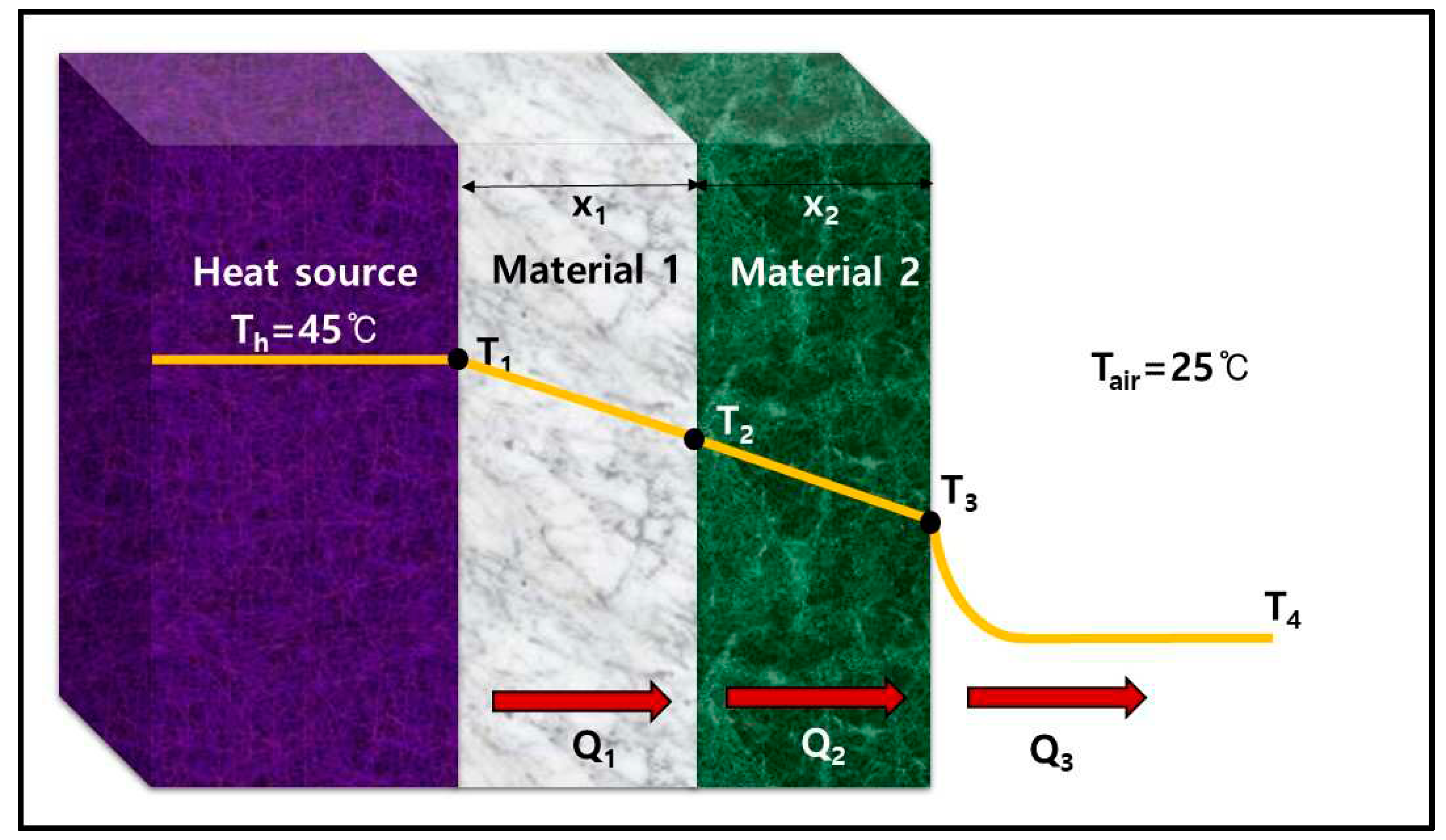
As shown in Figure 1 and Equation (11), for Material 1, the theory of heat transfer by conduction was used for calculation. The theory of heat transfer by convection and radiation was used in the calculation of Material 2.
Q = T 1 T 4 x 1 A k 1 + x 2 A k 2 + 1 ( h + ε σ ( T 3 2 + T 4 2 ) ( T 3 + T 4 ) ) A
In Equation (11), 'Q' represents the total heat transfer rate, Q1 and Q2 represent the heat transfer rates of Material 1 and Material 2, respectively, and Q3 represents the heat transfer rate to the atmosphere. Q=Q1=Q2=Q3, when calculated under normal conditions.
In addition, X1 and X2 represent the thickness ('k1') of Material 1 and Material 2(k2), ε represents the radiation rate, ' σ '' represents the Stefan-Boltzmann constant, and 'h' represents the heat transfer coefficient. The 'Q' value was derived using the trial and error method, and then the surface temperature was calculated. If the orientation of the metal sputtering specimen was changed, the figures for Material 1 and Material 2 were replaced for calculation [32]. It should be noted that the actual test material is fabric, but the calculation was carried out under the assumption that it was a solid material.
3. Results and Discussion

3.1. Surface Properties

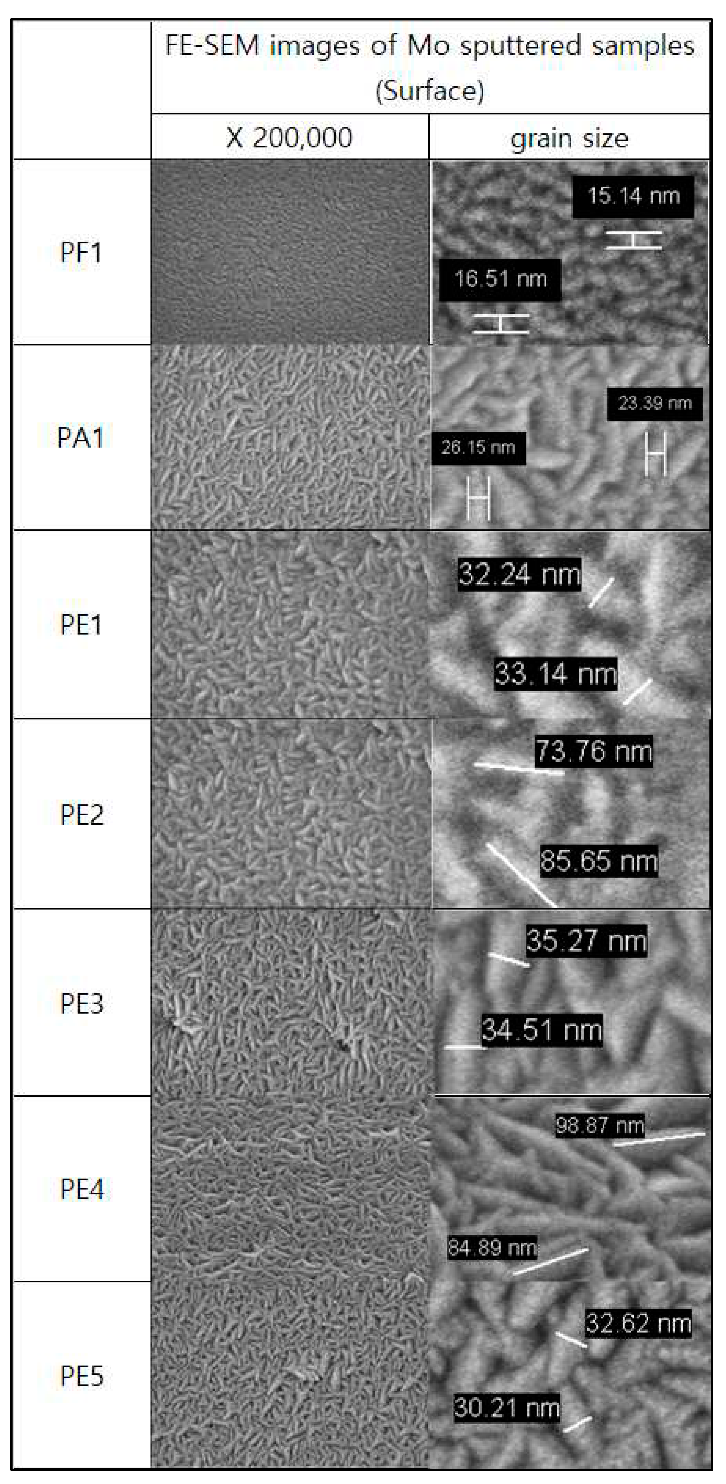
After molybdenum sputtering treatment, FE-SEM was performed to examine nano-formations on the sample (Figure 2). As a result, it was confirmed that the molybdenum layer was well applied to the surface of all sputtering-treated samples compared to the untreated samples. It can be observed that the surface of molybdenum in the form of corals formed in all specimens.
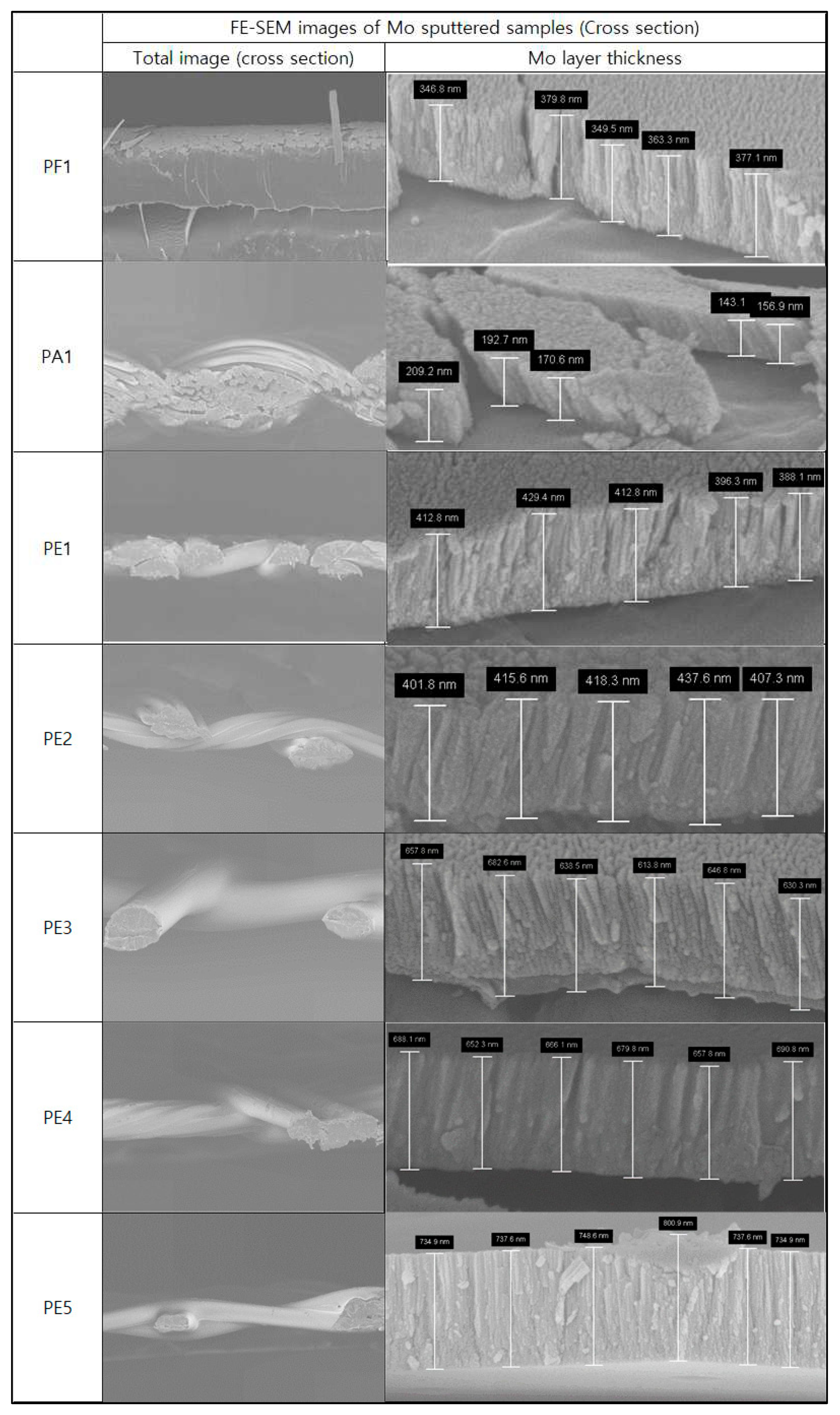
In addition, the cross-section FE-SEM was examined to observe in more detail what the thickness of the molybdenum particle layer on the sample was (Figure 3). In the case of PF1 and PA1, molybdenum layers with thicknesses ranging from 349.5 to 379.8 and from 143.1 to 209.2 nm were detected, respectively. In the case of PE1~5, the thickness of the molybdenum layer ranged from 388.1 to 429.4, 401.8 to 437.6, 613.8 to 682.6, 652.3 to 690.8, and 737.6 to 800.9 nm, respectively. In previous studies, when FE-SEM photography was performed after the metal sputtering treatment, nanograins were often observed on the surface [29,30], and in this study, they showed coral shapes rather than grain shapes on the surface. Since the sputtering time was longer than that of previous studies, it was judged that the molybdenum layer was more laminated to form a coral shape. The EDX results are as shown in Figure 4, and it was proved that molybdenum was well applied to the sample surface.

3.2. Electrical Resistance Properties

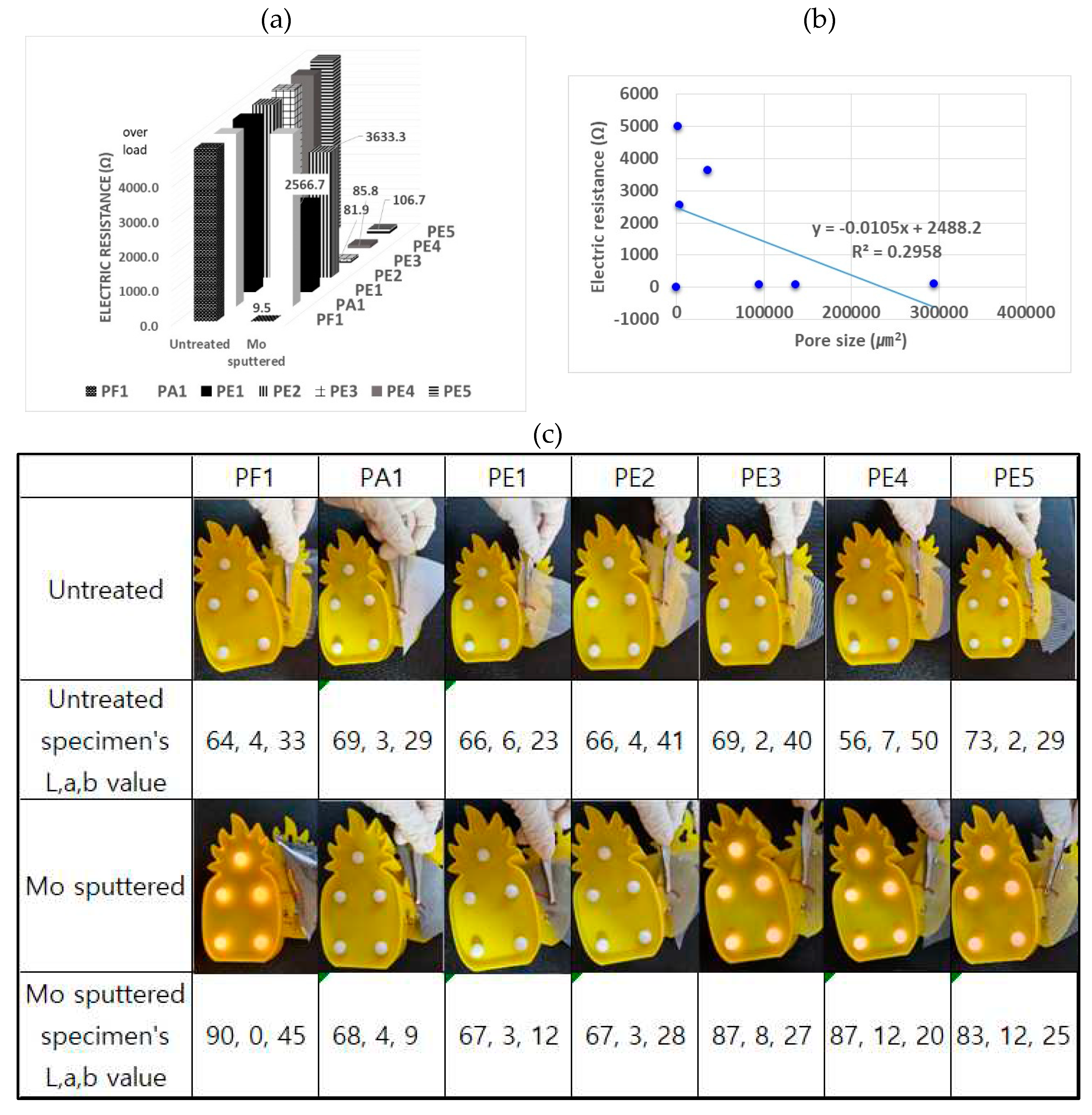
In the case of the electrical resistance of the molybdenum sputtering-treated sample, it is related to density and structure. Compared to the untreated sample, it was confirmed that the electrical resistance of the sputtering treatment net and the film sample was significantly reduced (Figure 5).
In the case of untreated samples, all PF1, NA1, and PE1 to PE5 samples showed an “overload” in which the electrical resistance exceeded the machine's measurement range. However, after the molybdenum sputtering treatment, the electrical resistance value (Ω) of all samples other than PA1 decreased significantly.
In the case of molybdenum sputtering PF1, the electrical resistance value was 9.5 Ω, and in the case of molybdenum sputtering PE1~5, the electrical resistance values were 2600, 3400, 83.5, 84.7, and 98 Ω, respectively. In Figure 4b, it was derived from the correlation equation between pore size and electrical resistance. The equation (12) is as follows.
Y=-0.0105x+2488.2 (12)
Similarly to previous studies [29,30], the electrical resistance of molybdenum sputtering PF1 was very low not because of a mirror deadlock, such as a plain weave or net, but because the surface is flat, the molybdenum layer is uniformly and flatly coated, and the current flows well without obstacles. In previous studies [29,30], even if sputtering was performed, the resistance of the sample was high except for the film, and in this study, the sputtering treatment time was five times longer than in previous studies. In this study, the sputtering treatment time of the PE1 to PE5 samples subjected to molybdenum sputtering is long, so it is believed that electrical resistance was expressed due to the thick thickness of the molybdenum coating layer.
In addition, prior research explained that the electrical value is insensitive to vacuum annealing conditions as all Mo films show somewhat the same value in the range of 3×10⁻⁵–6×10⁻⁵ Ωcm. It showed a similar tendency to the results of this study [31].
In addition, in other previous studies, electrical resistance was measured after molybdenum treatment, and the electrical resistance value was higher than in this study, indicating an "overload" outside the mechanical measurement. This study showed much smaller resistance than previous studies, and in previous studies, the molybdenum sputtering treatment time was 10 minutes, and in this study, the molybdenum layer was thicker with the sputtering time of 50 minutes [33].
However, in the case of PA1, PE1, and PE2 samples, the electrical resistance was relatively high even if molybdenum sputtering was performed under the same conditions. This is judged to have been cut off in the middle while the current was running because the light yarn was densely crossed, and the molybdenum layer was not thick enough to cover the light yarn furrow.
When molybdenum sputtering polyamide nets (PE3, 4, and 5) and a polyamide film (PF1) were placed between the LED bulk and the circuit, it was confirmed that the LED was lit (Figure 5). That is, it was confirmed that molybdenum sputtering polyamide stromal nets and films could be used as electrically conductive materials. The coating reduces electrical resistance. The polyamide film exhibited a significantly reduced electrical resistance value of 9.5 Ω due to the molybdenum sputtering treatment compared to other samples. As such, the electrical resistance has been greatly reduced, the possibility of application to electronic products has been proven. In addition, it is believed that the molybdenum sputtered polyamide film can be cut thin and used for sensors and precision electrical components.

3.3. Characteristics of IR Transmittance

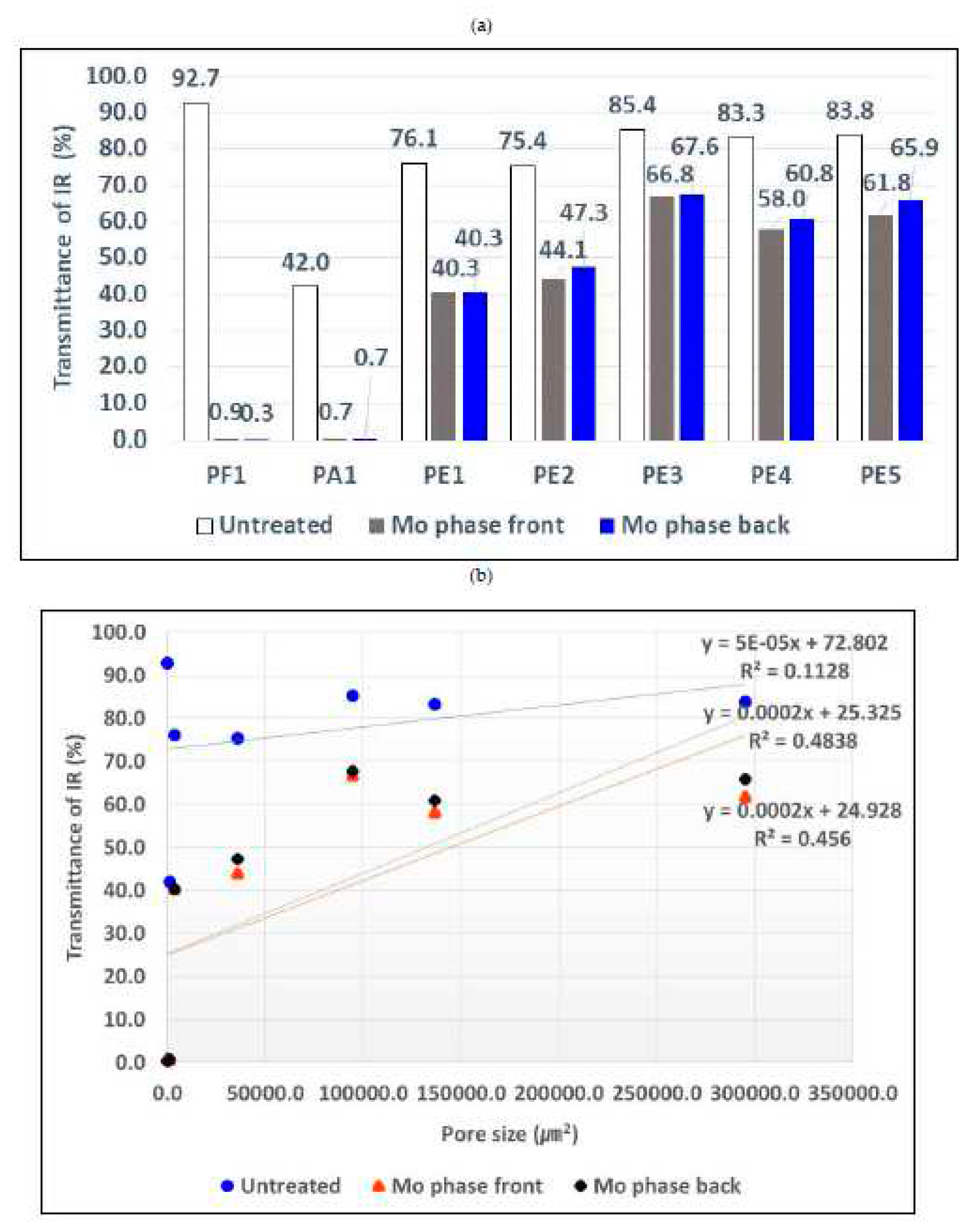
In this study, the IR transmittance measurement analysis of the untreated sample and the molybdenum sputtering-treated sample was conducted on only one side, and the results are shown in Figure 6. An IR irradiator was placed on the left, an IR measuring instrument was placed on the right, and a sputtering sample was placed between the irradiator and the measuring instrument; then, the analysis was performed. As a result of the measurement, the sample subjected to molybdenum sputtering showed a significant decrease in the infrared transmission value. The IR transmittance of the untreated sample ranged from 92.7 to 42.0%, which was very high.
However, when only the cross-section experienced molybdenum sputtering and the copper surface faces the IR irradiator (molybdenum phase front), the IR transmittance was 66.8 to 0.7%. In addition, when cross-sectional molybdenum sputtering is performed and the molybdenum surface faces the IR measuring instrument (molybdenum phase back), the IR transmittance ranged from 67.6 to 0.3%. In other words, the change in IR transmission value according to the direction of the molybdenum sputtering layer was not large, but the infrared transmission value was found to be very small when the molybdenum surface faced the IR irradiator. Additionally, as the density of the sample increased, the transmittance tended to increase. Previous studies have shown that the direction of the metal layer does not significantly affect the IR transmittance [29,30], and in this study, the thickness of the metal layer is thicker than in previous studies, so it is judged that there is a very small difference in the IR transmittance according to the direction of the metal layer.

3.4. IR Camera Stealth Function Based on Heat Transfer

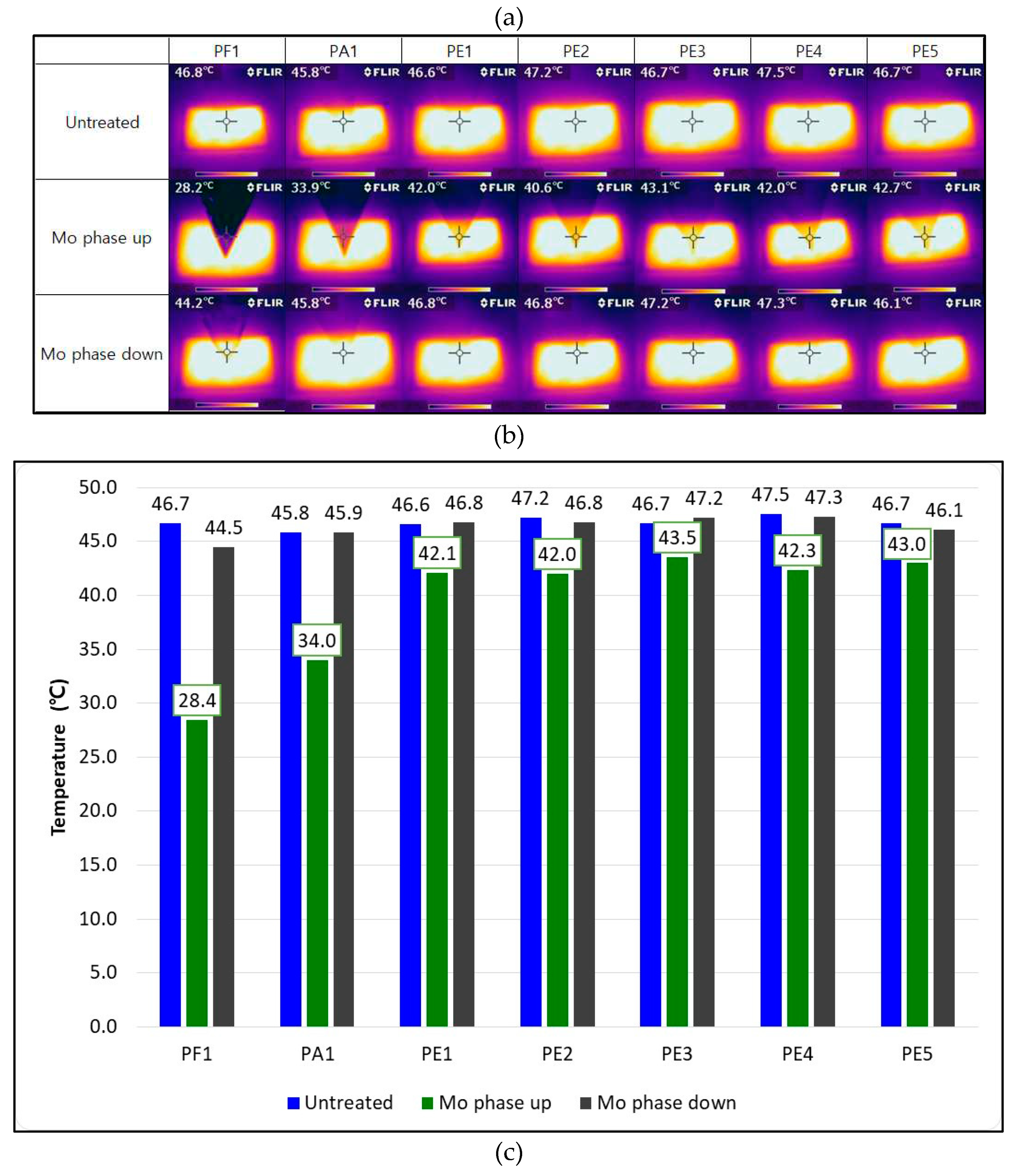
In this study, thermal characteristics based on high-temperature heat sources were examined using an infrared thermal imaging camera (Figure 7). The photograph was taken with an infrared thermal imaging camera at a distance of 0 cm (in a close state), and the photograph was taken while changing the direction of the sample to which only the cross-section experienced molybdenum sputtering. The surface temperature of the heat source ranged from 45.8 to 47.5°C.
In the case of a sputtering-treated sample on a film and a plain weave, when the molybdenum layer faces outside air, the surface temperature was much lower than the heat source. When the molybdenum layer of the molybdenum sputtering film was directed toward outside air, the surface temperature was 28.2℃, and when the molybdenum layer of the sputtering plain weave was directed toward the outside air, the surface temperature was 33.9℃. However, when the molybdenum layer part faces the heat source, the heat source's temperature appears on the infrared thermal imaging camera, and there was little stealth effect.
In addition, in the case of net samples, when the molybdenum-sputtered layer faced outside air, the net's appeal increased (PE1->PE5), the surface temperature ranged from 42.0 to 42.7℃, and the stealth effect decreased.
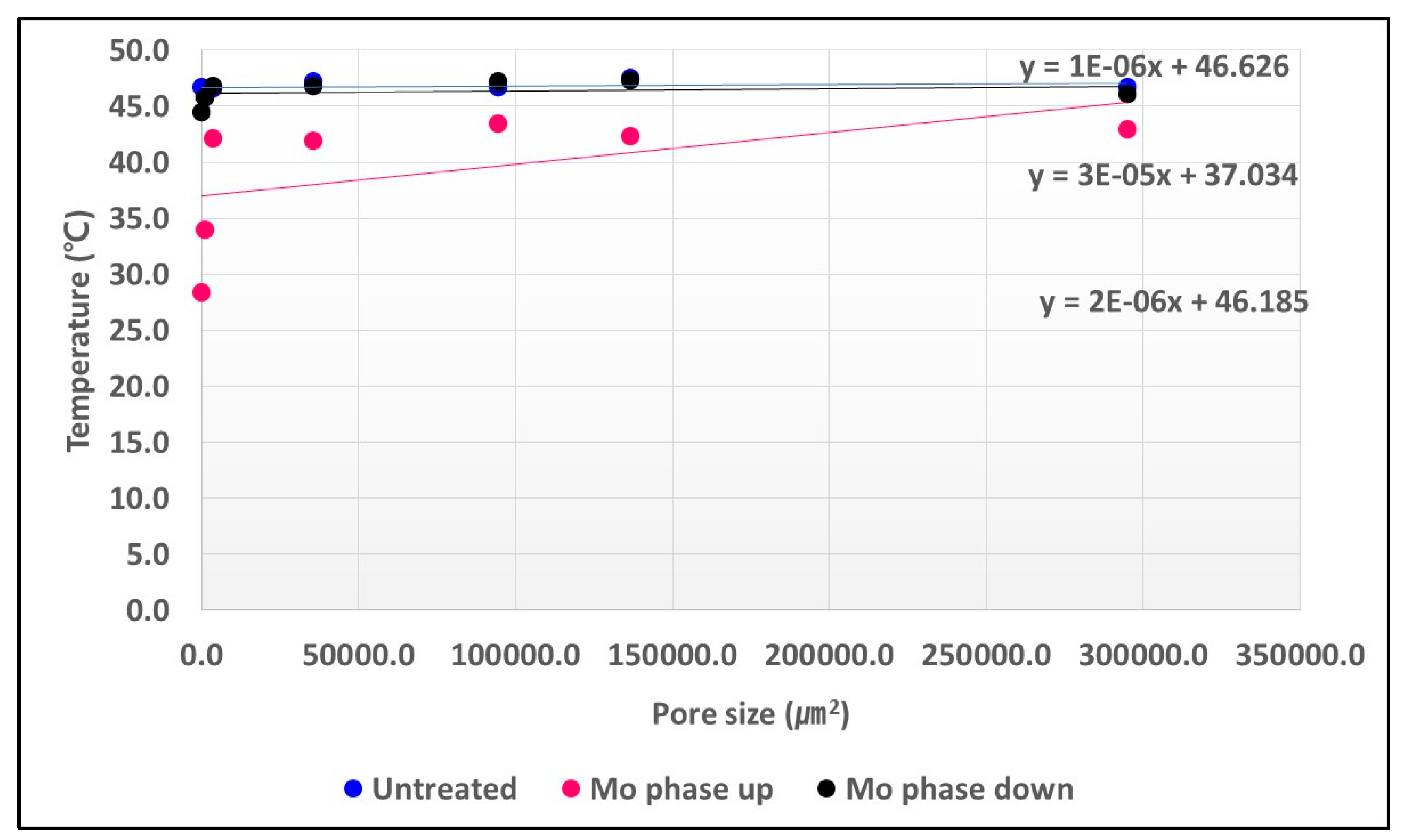
As the density of the net lowers and the pore size becomes larger, the heat of the heat source escapes to the outside air, and it is determined that the surface temperature is the same as the heat source temperature. In previous studies [29], when infrared thermal imaging was taken using sputtering-treated samples to direct the metal layer toward the outside air, the higher the density, the closer the surface temperature to the heat source. This study also showed a similar trend relative to previous studies. In addition, when the molybdenum layer part of the molybdenum sputtering-treated net sample faces the human body, the surface temperature ranged from 44.2 to 47.3℃, indicating a high surface temperature.
After taking an infrared thermal imaging camera, H, S, and V values were measured using a program to evaluate stealth effects using a quantitative IR camera (Table 3), and △H, △S, △V, and △E values were calculated (Table 4). The measurement point is the lower right part of the cross pattern shown in (a) of Figure 7.
Additionally, the values of △H, △S, △V, and △E were calculated according to Eq 1~3. The H, S, and V values of the outside air were "256, 40, 47", respectively, and the H, S, and V values of the heat source were "176, 6, 94", respectively.
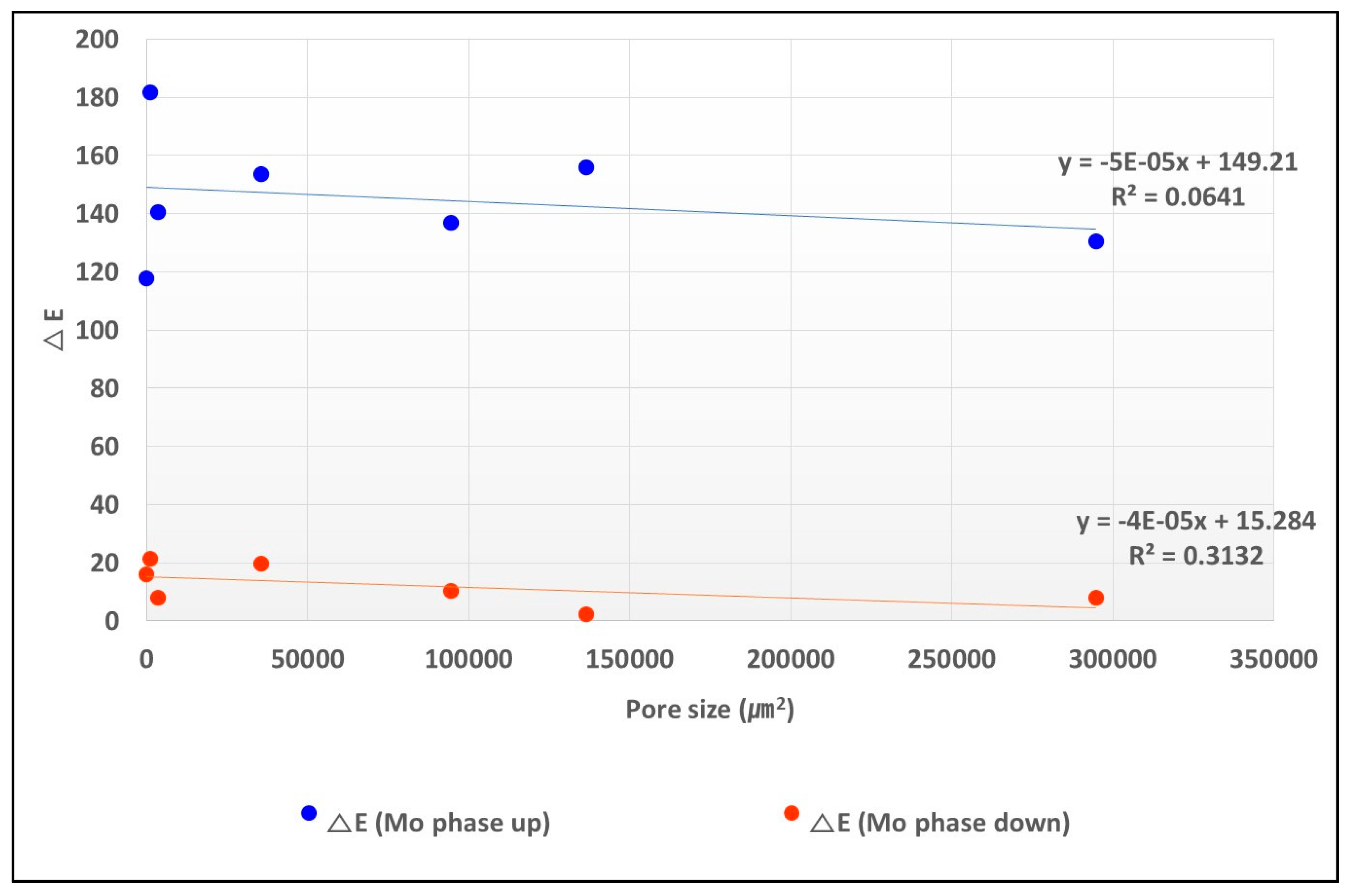
The values of H, S, and V of the “untreated sample” and “Molybdenum phase down” section (when the molybdenum surface of the cross-sectional sputtering-treated sample faces the human body) were very similar in all samples, and there was no significant difference depending on the density. For all samples in the untreated state, the H values were 147-168, the S values were 5-8, and the V values were 92-95. For all samples in the molybdenum phase-down section, the H value was 131–180, the S value was 4–6, and the V value was 92–100. This shows the same pattern as the thermal image of Figure 7. The small absolute value of △E (2.4~21.4) of the samples of the molybdenum phase-down section shows that the difference in H, S, and V values between the molybdenum phase-down sample and the untreated sample is small, and this explains that the stealth effect on the infrared thermal imaging camera is small. This shows the same pattern as the thermal image of Figure 7.
On the other hand, the HSV value of the “Molybdenum phase up (when the copper surface of the cross-sectional sputtering treatment sample faces the outside air)” section showed a different tendency in contrast to the “untreated sample” and “Molybdenum phase down” section. For the data of all samples in the molybdenum phase-up section, the H value was 31-321, the S value was 31-90, and the V value was 41-99. In the case of the H value, the density of the sample decreased (PF1->PE5). In the case of the V value, the density of the sample increased (PF1->PE5).
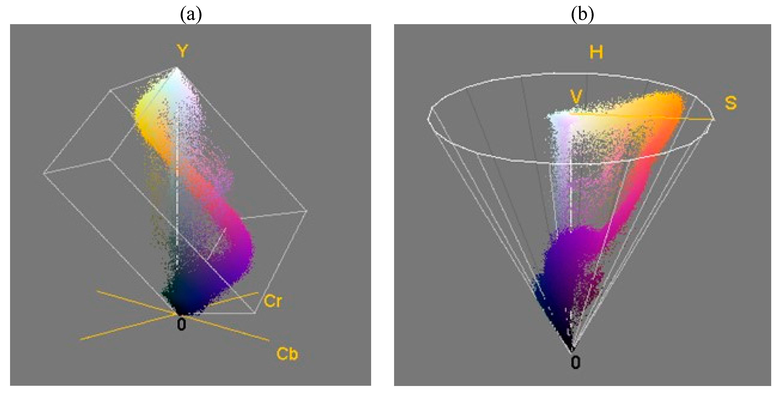
The large absolute value of △ E (117.9 to 181.7) of the molybdenum phase-up sample shows that the difference in H, S, and V values between the molybdenum phase-up sample and the untreated sample is large. This is evidence that the molybdenum phase-up sample has an alternative stealth effect on infrared thermal imaging detectors. The HSV cone model is a more realistic modification of the cylindrical model. Since 0% brightness means only black, it is expressed as a single point and corresponds to the vertex of the cone. In addition, the darker the actual color, the less the color change due to the change in the saturation value, so the width represented by the saturation value is reduced compared to the high brightness. The cone model reflects this fact in the cylindrical model. Looking at the figure on the right, it can be seen that the saturation change is wide at high brightness and the saturation change is not large at low brightness.
Figure 8. (a) Three-dimensional color distribution of HSV; (b) 3D color distribution of YCbCr.
Preprints 73517 g008
Figure 9. Correlation between pore size and △E.
Preprints 73517 g009
After taking infrared thermal imaging photos, the Y, Cb, and Cr values were measured using a program (Color Inspector 3D, Image J) to evaluate stealth effects on quantitative IR cameras (Table 5), and △Y, △Cb, and △Cr values were calculated (Table 6). For values of △Y, △Cb, △Cr, and △T, the aforementioned expressions in "Eq. 4~7" describe them. The Y, Cb, and Cr values of “untreated samples” and the “Molybdenum phase down (when the molybdenum surface of the cross-sectional sputtering sample faces the heat source)” section were very similar regardless of density in all samples, and there was no significant difference in density. For all samples in the untreated state, the Y values ranged from 234 to 241, Cb values ranged from -3 to 1, and Cr values ranged from -9 to -7. The Y values of all samples in the molybdenum phase-down section were 206-248, the Cb values were -16-1, and the Cr values were -8~-1. The fact that the absolute values of △Y, △Cb, and △Cr of the samples of the molybdenum phase-down section are 2~28, 0~14, and 0~8, respectively, shows that the difference in Y, Cb, and Cr values between the molybdenum phase-down sample and the untreated sample is small, and it explains the stealth effect on the infrared thermal imaging detector.
On the other hand, the Y, Cb, and Cr values of the “Molybdenum phase up” section (when the molybdenum surface of the cross-sectional sputtering treatment sample faces outside air) showed a different pattern compared to the “untreated sample” and “Molybdenum phase down.” For the data of all samples in the molybdenum phase-up section, the Y value was 26 to 210, the Cb value was -96 to 26, and the Cr value was -17 to 62.
In the case of the Y value, the density of the sample increased (PF1->PE5). The absolute values of △Y, △Cb, and △Cr in the molybdenum phase-up section were 31~208, 6~95, and 8~69, respectively, and in the case of △T value, the denser the sample density (PE5->PF1), the greater the absolute value. The large absolute values of △Y, △Cb, and △Cr show that the difference in Y, Cb, and Cr values between the molybdenum phase-up sample and the untreated sample is large. This argues that the dense molybdenum phase-up sample has an alternative stealth effect on infrared thermal imaging detectors.
Figure 10. Correlation between pore size and △T.

3.5. Theoretical Analysis of Heat Transfer

The study deduced each phase temperature of the Molybdenum sputtered specimens in the steady state according to the heat transfer theory. The numerical values used for calculation are seen in Table 7. In case of thickness, the actual measured values (Figure 3) were used, and in case of metal thermal conductivity and emissivity, reference values were employed. Also, such reference values were utilized for the nylon fabric’s thermal conductivity, emissivity and heat transfer coefficient. The heat transfer coefficients of the metals used for sputtering were calculated using the trial and error method based on the surface temperatures and the values of Table 7. If a molybdenum layer formed by sputtering has a coral shaped surface, it results in an increase in the specific surface area. Then, it becomes more difficult to calculate the heat transfer coefficient of a metal with an increased specific surface area than that of a metal with a flat surface. For this reason, the computed values were used.
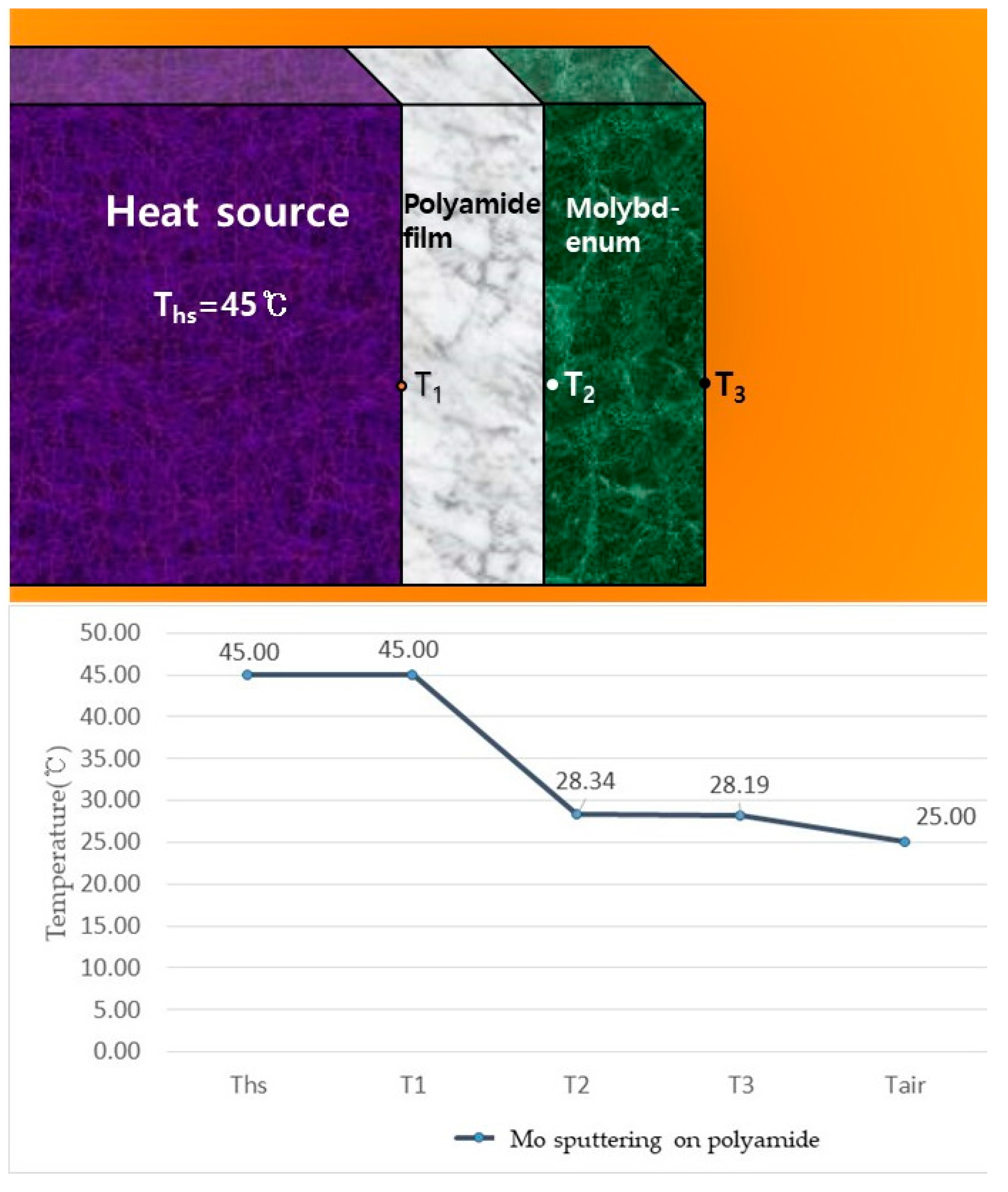
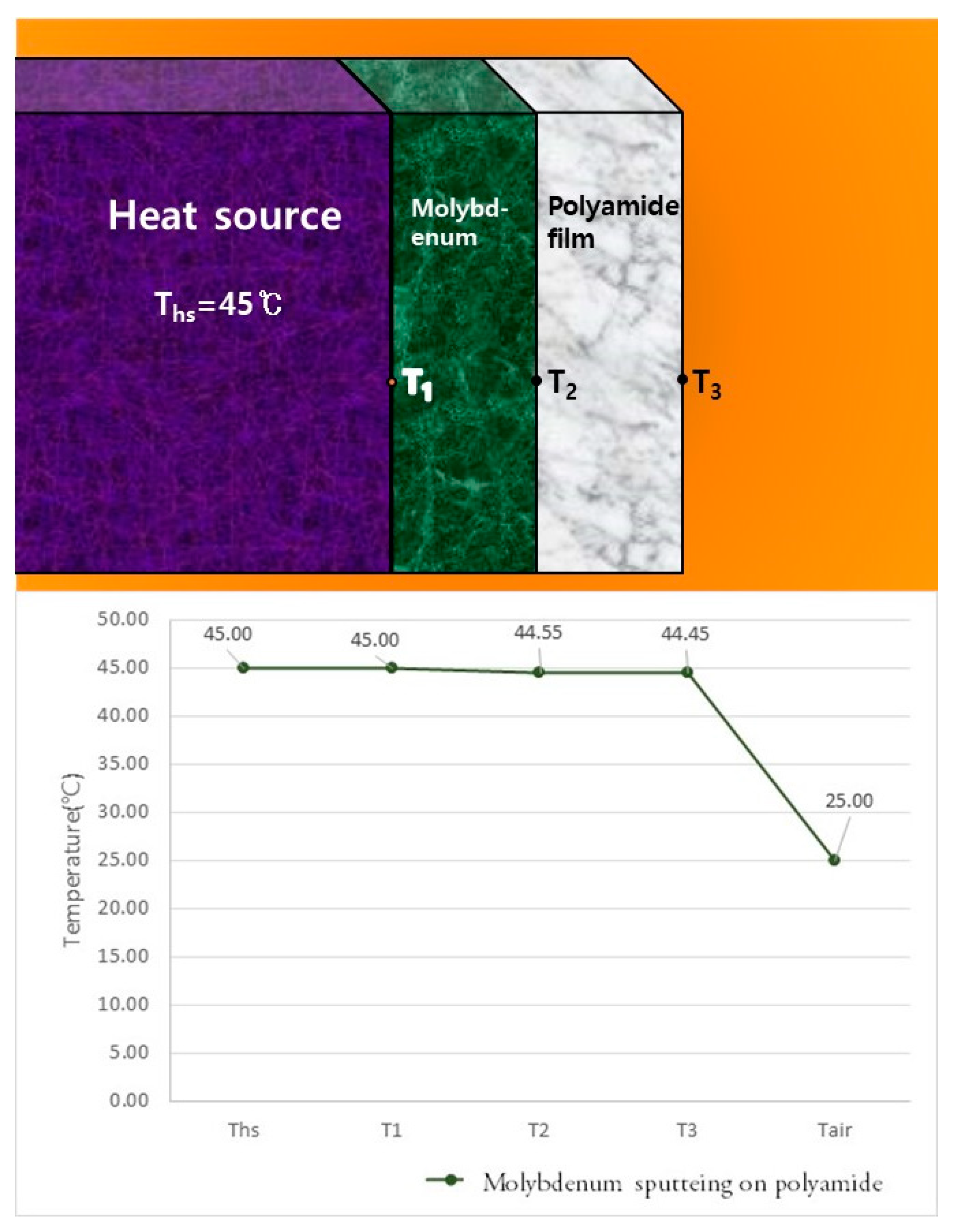
In case of the molybdenum equation based on data in the literature [00] was used to identify a heat transfer coefficient adequate to the study specimens’ thickness of the molybdenum layer. When the molybdenum-sputtered fabric’s metal layer pointed to the outside air (Figure 11), the heat transfer rate (Q) was high at 5748.3W, and T2 and T3 subsequently had low temperatures (28.34 ℃ and 28.18 ℃, respectively). In contrast, if the molybdenum sputtered film’s metal layer of the pointed toward the heat source (Figure 12), the heat transfer rate (Q) was low at 187.1W and therefore, T2 and T3 had temperatures (44.55, 44.45 ℃) similar to the heat source.
If molybdenum layers were directed toward the heat source, T2 and T3 were found to be almost the same. The theoretically inferred surface temperature (T3) was very consistent with the actual values mentioned above. The heat transfer rate was significantly greater in Q value (or greater heat loss) when pointing to outside air than when the metal layer pointed to the heat source.

4. Conclusions

In this study, electrical characteristics, IR transmission characteristics, stealth functions for infrared thermal imaging detectors, and the thermal characteristics of molybdenum sputtering treatment samples were studied. Polyamide samples were prepared by density (five types by polyamide film, polyamide plain weave, and polyamide net pore size) as base materials for molybdenum sputtering treatments.
In addition, IR transmittance, electrical characteristics, H, S, V, Y, Cb, Cr, and surface temperature changes when photographing infrared thermal imaging cameras according to sample density were evaluated, and these were considered in depth. As a result of measuring the electrical resistance for evaluating electrical resistance, untreated samples exhibited a high resistance value to the extent of deviating from the measured values in all samples, and electrical resistance value was very high. However, in the case of molybdenum sputtering-treated PF1 and PE1~5, the electrical resistance was very low compared to the untreated sample.
In addition, when molybdenum sputtering samples were placed and connected between the LED light and the battery, the LED was lit at PF1 and from PE3 to 5. This is believed to be due to the low electrical resistance resulting from the molybdenum sputtering treatment. Additionally, in the case of net samples, the higher the density, the lower the electrical resistance.
As a result of measuring the IR transmittance, the infrared transmittance of the molybdenum sputtering-treated sample was significantly reduced compared to the untreated sample. In the case of untreated samples, the transmittance was 92.7 to 42.0%. When only the cross part was treated with molybdenum sputtering and the molybdenum surface was directed to the IR irradiator, the IR transmittance was 66.8~0.7%. In addition, when the molybdenum surface faced the IR measuring device, the IR transmittance ranged from 67.6 to 0.3%. That is, the change in the IR transmission value according to the direction of the molybdenum sputtering layer was not large. Additionally, as the density of the sample increased, the transmittance tended to increase.
In the infrared thermal imaging camera image, in the case of the net sample, when the molybdenum-sputtered layer faced outside, the surface temperature of the net was 42.0~42.7℃, and the stealth effect decreased. As the density of the net increases and pore size increases, heat from the human body escapes, and the surface temperature appears as the heat source's temperature.
After using an infrared thermal imaging camera, the stealth effect evaluation with a quantitative IR camera was performed by measuring H, S, V, Y, Cb, and Cr values and calculating △H, △S, △V, △Y, △Cb, and △Cr values. The fact that the absolute value of △ E (2.4~21.4) of the samples of the molybdenum phase-down section is small explains that the difference in the H, S, and V values between the molybdenum phase-down sample and the untreated sample is small. The large absolute value of △ E (117.9 to 181.7) of the molybdenum phase-up section shows that the difference in H, S, and V values between the molybdenum phase-up sample and the untreated sample is large. This shows that the molybdenum phase-up sample has an alternative stealth effect on the infrared thermal imaging detector. Considering the aforementioned IR transmission characteristics and the results of H, S, V, Y, Cb, and Cr, the direction of the molybdenum sputtering layer in all samples did not significantly affect the infrared transmission rate. It is judged that the IR transmittance does not significantly affect the stealth effect.
This study calculated each phase temperature of the Molybdenum sputtered specimens in the steady state according to the heat transfer theory. When the molybdenum-sputtered fabric’s metal layer pointed to the outside air (Figure 11), the heat transfer rate (Q) was high at 5748.3W, and T2 and T3 subsequently had low temperatures (28.34 ℃ and 28.18 ℃, respectively). In contrast, if the molybdenum sputtered film’s metal layer of the pointed toward the heat source (Figure 12), the heat transfer rate (Q) was low at 187.1W and therefore, T2 and T3 had temperatures (44.55, 44.45 ℃) similar to the heat source.
It is believed that the molybdenum sputtering polyamide samples produced in this study can be applied to multifunctional military uniforms, breathing sensors, biosignal detection sensors, semiconductor products, batteries, etc., by utilizing excellent electrical properties, stealth functions, IR blocking properties, and lightness for infrared thermal imaging detectors.

Conflicts of Interest

The authors declare no conflicts of interest.

References

  1. Badding, E.D.; Srisantitham, S.; Lukoyanov, D.A.; et al. Connecting the geometric and electronic structures of the nitrogenase iron–molybdenum cofactor through site-selective 57Fe labelling. Nat. Chem. 2023. [Google Scholar] [CrossRef] [PubMed]
  2. KuO, K.; Hagg, G. A. New Molybdenum Carbide. Nature 1952, 170, 245–246. [Google Scholar] [CrossRef]
  3. Spackman, J. Electron Spin Resonance of Charge Carriers in Impure Molybdenum Disulphide. Nature 1963, 198, 1266–1267. [Google Scholar] [CrossRef]
  4. Ashida, Y.; Mizushima, T.; Arashiba, K.; et al. Catalytic production of ammonia from dinitrogen employing molybdenum complexes bearing N-heterocyclic carbene-based PCP-type pincer ligands. Nat. Synth 2023. [Google Scholar] [CrossRef]
  5. Li, Z.; Sami, I.; Yang, J.; et al. Lithiated metallic molybdenum disulfide nanosheets for high-performance lithium–sulfur batteries. Nat Energy 2023, 8, 84–93. [Google Scholar] [CrossRef]
  6. Wang, H.; Zhang, C.; Chan, W.; et al. Ultrafast response of monolayer molybdenum disulfide photodetectors. Nat Commun 2015, 6, 8831. [Google Scholar] [CrossRef] [PubMed]
  7. Wei, H.; Huan, S.; Fei, X.; Jian, W. A review and perspective on molybdenum-based electrocatalysts for hydrogen evolution reaction. Rare Metals 2020, 39, 335–351. [Google Scholar]
  8. Okotrub, A.V.; Sedelnikova, O.V.; Gorodetskiy, D.V.; Fedorenko, A.D.; Asanov, I.P.; Palyanov, Y.N.; Lapega, A.V.; Gurova, O.A.; Bulusheva, L.G. Effect of Titanium and Molybdenum Cover on the Surface Restructuration of Diamond Single Crystal during Annealing. Materials. 2023, 16, 1650. [Google Scholar] [CrossRef]
  9. Ali, A.; Piatkowski, P.; Nawaz, T.; Ahmad, S.; Ibrahim, T.; Khamis, M.; Alnaser, AS. A Two-Step Femtosecond Laser-Based Deposition of Robust Corrosion-Resistant Molybdenum Oxide Coating. Materials. 2023, 16, 909. [Google Scholar] [CrossRef]
  10. Candela, V.; Cavallini, C.; Gasparrini, C.; Armelao, L.; Candeloro, V.; Dalla, P.M.; Fadone, M.; Marcuzzi, D.; Pavei, M.; Pepato, A.; Pouradier, D. B.; Rancan, M.; Rizzolo, A.; Sartori, E.; Segalini, B.; Serianni, G.; Spolaore, M.; Zorzi, F.; Sonato, P. Investigations on Caesium Dispersion and Molybdenum Coating on SPIDER Components. Materials. 2023, 16, 206. [Google Scholar] [CrossRef]
  11. Santagata, A.; Pace, M.L.; Bellucci, A.; Mastellone, M.; Bolli, E.; Valentini, V.; Orlando, S.; Sani, E.; Failla, S.; Sciti, D.; Trucchi, D.M. Enhanced and Selective Absorption of Molybdenum Nanostructured Surfaces for Concentrated Solar Energy Applications. Materials. 2022, 15, 8333. [Google Scholar] [CrossRef] [PubMed]
  12. Thompson, M. Mechanisms of sputtering. Nature 1979, 277, 326–327. [Google Scholar] [CrossRef]
  13. Strachan, J.; Harris, N. X-Ray Hazard in Sputtering Apparatus. Nature 1956, 178, 588–589. [Google Scholar] [CrossRef] [PubMed]
  14. Pollitt, K.; Robb, J.; Thomas, D. Mechanism of sputtering of solid surfaces by ion-impact. Nature 1978, 272, 436–437. [Google Scholar] [CrossRef]
  15. Haff, P.; Seiberling, L. Anomalous sputtering at high energy. Nature 1981, 290, 544–545. [Google Scholar] [CrossRef]
  16. Han, H.R. Hybrid Fiber Materials according to the Manufacturing Technology Methods and IOT Materials: A Systematic Review. Materials 2023, 16, 1351. [Google Scholar] [CrossRef]
  17. Grenadyorov, A.; Oskirko, V.; Zakharov, A.; Oskomov, K.; Rabotkin, S.; Semenov, V.; Solovyev, A.; Shmakov, A. Properties of TiAlN Coatings Obtained by Dual-HiPIMS with Short Pulses. Materials 2023, 16, 1348. [Google Scholar] [CrossRef]
  18. Za’abar, F‘I.; Mahmood, Z.A.W.; Doroody, C.; Chelvanathan, P.; Yusoff, Y.; Abdullah, S.F.; Bahrudin, M.S.; Wan, A.W.S.; Ahmad, I.; Wan, A.W.S.; Amin, N. Probing the Interplay between Mo Back Contact Layer Deposition Condition and MoSe2 Layer Formation at the CIGSe/Mo Hetero-Interface. Materials 2023, 16, 2497. [Google Scholar] [CrossRef]
  19. Andrulevičius, M.; Artiukh, E.; Suchaneck, G.; Wang, S.; Sobolev, N.A.; Gerlach, G.; Tamulevičienė, A.; Abakevičienė, B.; Tamulevičius, S. Multitarget Reactive Magnetron Sputtering towards the Production of Strontium Molybdate Thin Films. Materials. 2023, 16, 2175. [Google Scholar] [CrossRef]
  20. Lan, N.; Pham, G.F.; Tabor, A.P.; Jacob, L. B.; Aman, T. H.; Jake, J. A. Dexterous magnetic manipulation of conductive non-magnetic objects. Nature. 2021, 598, 439–443. [Google Scholar]
  21. Yongyi, Z.; Yunsik, O.; Jiahe, L.; Yichi, L.; Huai, C.; Phillip, W.; Peter, R.; Manuel, R. C.; Mohammad, F. I.; Jung, H. A.; Lynn, M.W.; Carmel, M. A self-healing electrically conductive organogel composite. Nature electronics 2023. Available online: https://www.nature.com/articles/s41928-023-00932-0.
  22. Bartlett, M. D.; Dickey, M. D.; Majidi, C. Self-healing materials for soft-matter machines and electronics. NPG Asia Mater. 2019, 11, 21. [Google Scholar] [CrossRef]
  23. Yu, X.; et al. Highly stretchable, ultra-soft and fast self-healable conductive hydrogels based on polyaniline nanoparticles for sensitive flexible sensors. Adv. Funct. Mater. 2022, 32, 2204366. [Google Scholar] [CrossRef]
  24. Polachan, K.; Chatterjee, B.; Weigand, S.; Sen, S. Human body-electrode interfaces for wide-frequency sensing and communication: a review. Nanomaterials 2021, 11, 2152. [Google Scholar] [CrossRef] [PubMed]
  25. Zeissler, K. Electrical control of qubits speeds up. Nat Electron 2023, 6, 103. [Google Scholar] [CrossRef]
  26. Ahmad, M.; Ha, JH.; Mayse, L.A.; et al. A generalizable nanopore sensor for highly specific protein detection at single-molecule precision. Nat Commun 2023, 14, 1374. [Google Scholar] [CrossRef] [PubMed]
  27. Chen, A.; Brand, H.; Helbig, T.; et al. Hyperbolic matter in electrical circuits with tunable complex phases. Nat Commun 2023, 14, 622. [Google Scholar] [CrossRef]
  28. Meloni, M.; Large, M.J.; González, D.J.M.; et al. Explosive percolation yields highly-conductive polymer nanocomposites. Nat Commun 2022, 13, 6872. [Google Scholar] [CrossRef]
  29. Han, H.R. A study on the thermal and electrical conductivity properties of titanium sputtered materials. Journal of the Korean Society of Clothing and Textiles 2022, 46, 530–544. [Google Scholar] [CrossRef]
  30. Han, H.R. Stealth, electromagnetic interception, and electrical properties of aluminum sputtered clothing materials - Focusing on the density change. The Research Journal of the Costume Culture 2022, 30, 579–593. [Google Scholar] [CrossRef]
  31. Chelvanathan, P.; Zakaria, Z.; Yusoff, Y.; Akhtaruzzaman, M.; Alam, M.M.; Alghoul, M.A.; Sopian, K.N. Amin Annealing effect in structural and electrical properties of sputtered Mo thin film. Applied Surface Science 2015, 334, 15–129. [Google Scholar] [CrossRef]
  32. Han, H. R.; Kim, J. J. A study on the thermal and physical properties of nylon fabric treated by metal sputtering (Al, Cu, Ni). Textile Research Journal. 2018, 88, 2397–2414. [Google Scholar] [CrossRef]
  33. Han, H. R. A study on thermal and electrical properties of molybdenum sputtered clothing materials. The Research Journal of the Costume Culture. 2022, 30, 2383–6334. [Google Scholar] [CrossRef]
  34. Wang, L.; Dong, J.; Zhang, W.; Zheng, C.; Liu, L. Deep Learning Assisted Optimization of Metasurface for Multi-Band Compatible Infrared Stealth and Radiative Thermal Management. Nanomaterials. 2023, 13, 1030. [Google Scholar] [CrossRef] [PubMed]
  35. Jia, J.; Han, Z.; Liu, L.; Xie, H.; Lv, M. Design Principle of RF Stealth Anti-Sorting Signal Based on Multi-Dimensional Compound Modulation with Pseudo-Center Width Agility. Electronics. 2022, 11, 4027. [Google Scholar] [CrossRef]
  36. Xi, Z.; Binjie, X.; Zhuoming, C.; Xiaoxiao, P.; Tingitng, Z; Jia, Y. Preparation of PANI-coated hollow glass microsphere and its application in dual-band stealth coated fabric. Polymer Bulletin, 2021, 79, 7555–7570. [Google Scholar] [CrossRef]
  37. Jiaheng, H.; Yan, H.; Yinghua, Y.; Ruiqi, S. Unique applications of carbon materials in infrared stealth: A review. Chemical Engineering Journal 2023, 452. [Google Scholar] [CrossRef]
  38. Xi, Z.; Binjie, X.; Yan, L. Research progress on infrared stealth fabric. Journal of Physics: Conference Series 2021, 1790. [Google Scholar] [CrossRef]
  39. Salah, M. S.; Ahmed, F. G.; Hanaa, A. S. Thermal Radiations Mitigation and Stealth using Egyptians Cotton Fabrics Treated with ZnO Nanoparticles and Chlorophyll. International Journal on Advanced Science, Engineering and Information Technology, 2022, 8, 2314–2322. [Google Scholar] [CrossRef]
Figure 1. Multi layer materials and heat transfer simulation.
Preprints 73517 g001
Figure 2. Surface characteristics of molybdenum-sputtered specimens.
Preprints 73517 g002
Figure 3. Cross-section characteristics of molybdenum-sputtered specimens.
Preprints 73517 g003
Figure 4. EDX results of Mo-sputtered specimens: (a) PF1; (b) PA1; (c)PE1.
Preprints 73517 g004
Figure 5. Electrical resistance of specimens: (a) electrical resistance of untreated and molybdenum-sputtered specimens; (b) correlation between pore size and electrical resistance; (c) LED bulb lighting comparison between untreated and molybdenum-sputtered specimens.
Preprints 73517 g005
Figure 6. Transmittance of IR: (a) transmittance of IR according to untreated and molybdenum-sputtered specimens; (b) correlation between pore size and IR transmittance.
Preprints 73517 g006
Figure 7. (a) IR thermal images of untreated and sputtered specimens (b) Surface temperature for untreated and sputtered specimens (c) Correlation of Pore size and surface temperature.
Preprints 73517 g007aPreprints 73517 g007b
Figure 11. Calculated surface temperature (Molybdenum phase up).
Preprints 73517 g011
Figure 12. Calculated surface temperature (Molybdenum phase down).
Preprints 73517 g012
Table 1. Information on base materials.
  Polyamide film Polyamide plain weave(textile) Polyamide net1 Polyamide net2 Polyamide net3 Polyamide net4 Polyamide net5
Sample code PF1 PA1 PE1 PE2 PE3 PE4 PE5
Sample thickness (mm) 0.09 0.15 0.08 0.10 0.15 0.11 0.19
Structure type Flat Plain weave Net Net Net Net Net
Pore size(2) 0 1200 3564 35696.3 94440.4 136476.2 294825.5
Table 2. Molybdenum sputtering conditions.
Process 50 (nm/minute)
Time 1200sec (20min)
Process pressure (Torr) 6m Torr
Gas (sccm) Ar 40 sccm
Power (W) DC 500 W
Machine SRN-120
Table 3. H, S, and V results of untreated and molybdenum-sputtered specimens.
  Untreated Mo phase up Mo phase down
H S V H S V H S V
PF1 147 8 95 249 32 41 131 6 94
PA1 147 7 95 321 54 72 168 6 99
PE1 168 6 94 43 70 90 160 5 95
PE2 161 7 95 31 89 98 180 4 100
PE3 158 6 95 45 83 93 168 6 92
PE4 167 7 95 35 90 99 168 5 96
PE5 160 5 92 50 75 94 168 6 93
Table 4. △H, △S, and △V results according to IR thermal images.
   Mo phase up Mo phase down
△H △S △V △E △H △S △V △E
PF1 102 24 -54 117.9 -16 -2 -1 16.2
PA1 174 47 -23 181.7 21 -1 4 21.4
PE1 -125 64 -4 140.5 -8 -1 1 8.1
PE2 -130 82 3 153.7 19 -3 5 19.9
PE3 -113 77 -2 136.8 10 0 -3 10.4
PE4 -132 83 4 156.0 1 -2 1 2.4
PE5 -110 70 2 130.4 8 1 1 8.1
Table 5. Y, Cb, and Cr results of untreated and molybdenum-sputtered specimens.
Untreated Mo phase up Mo phase down
Y Cb Cr Y Cb Cr Y Cb Cr
PF1 234 -2 -9 26 4 -17 206 -16 -1
PA1 237 -3 -7 95 26 62 248 1 -7
PE1 235 -1 -9 159 -75 54 237 0 -8
PE2 236 0 -8 173 -95 57 239 1 -7
PE3 240 0 -8 184 -89 39 218 1 -7
PE4 240 1 -9 186 -96 40 233 1 -7
PE5 241 0 -7 210 -67 19 238 1 -7
Table 6. △Y, △Cr, △Cb, and △T values according to the IR thermal image.
   Mo phase up Mo phase down
△Y △Cb △Cr △T △Y △Cb △Cr △T
PF1 -208 6 -8 208.2 -28 -14 8 32.3
PA1 -142 29 69 160.5 11 4 0 11.7
PE1 -76 -74 63 123.4 2 1 1 2.4
PE2 -63 -95 65 131.2 3 1 1 3.3
PE3 -56 -89 47 115.2 -22 1 1 22.0
PE4 -54 -97 49 121.4 -7 0 2 7.3
PE5 -31 -67 26 78.3 -3 1 0 3.2
Table 7. Characteristics of materials for calculation.
Thickness(nm) Thermal conductivity(W/mk) Emissivity(%)
Molybdenum 363.3 138 0.74
Polyamide film 90X10-6 3.08 X10⁻² 0.85
Disclaimer/Publisher’s Note: The statements, opinions and data contained in all publications are solely those of the individual author(s) and contributor(s) and not of MDPI and/or the editor(s). MDPI and/or the editor(s) disclaim responsibility for any injury to people or property resulting from any ideas, methods, instructions or products referred to in the content.
Copyright: This open access article is published under a Creative Commons CC BY 4.0 license, which permit the free download, distribution, and reuse, provided that the author and preprint are cited in any reuse.
Prerpints.org logo

Preprints.org is a free preprint server supported by MDPI in Basel, Switzerland.

Subscribe

© 2024 MDPI (Basel, Switzerland) unless otherwise stated