Submitted:
16 May 2023
Posted:
17 May 2023
You are already at the latest version
Abstract
Keywords:
1. Introduction
2. Design





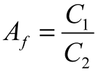
2.2. Neurostimulator
3. Experimental Results
3.1. LNA
3.2. Neurostimualtor Circuit

4. Conclusions

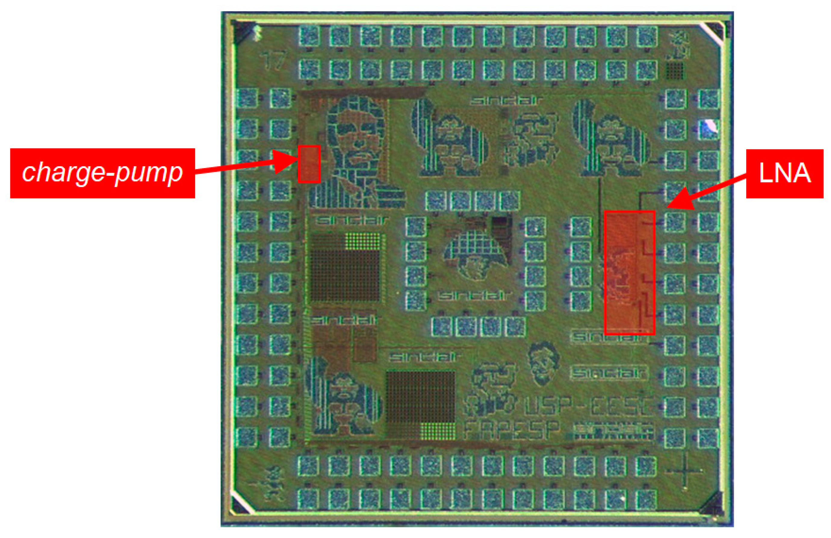
Author Contributions
Funding
Acknowledgments
Conflicts of Interest
References
- Appleby, B.S.; Duggan, P.S.; Regenberg, A., and P. V. Rabins. Psychiatric and Neuropsychiatric Adverse Events Associated With Deep Brain Stimulation: A Meta-analysis of Ten Years’ Experience. Movement Disorders 2007, 22, 1722–1728. [CrossRef] [PubMed]
- Sui; Y; Tian; Y.; Ko; W.K.D.; Wang; Z.; Jia; F.; Horn; A.; de Ridder; D.; Choi; K.S.; Bari; A.A.; Wang, S.; et al. Deep brain stimulation initiative: Toward innovative technology, new disease indications, and approaches to current and future clinical challenges in neuromodulation therapy. Front. Neurol. 2021, 11, 59745.
- Medtronic DBS Therapy for Parkinson’s Disease, Medtronic Inc., Catalog UC201607188bEE. 2020. Available online: https://asiapac.medtronic.com/content/dam/medtronic-com/uk-en/patients/documents/parkinsons-disease/pd-brochure-uc201607188ee.pdf?bypassIM=truelead (accessed on 5 March 2022).
- Hickey; P; Stacy, M. Deep Brain Stimulation: A Paradigm Shifting Approach to Treat Parkinson’s Disease. Front. Neurosci. 2016, 10, 173.
- VerciseTM DVBS Leads: Directions for Use, Boston Scientific Corporation, Catalog 91172963-02 REV A 2017-02. 2017. Available online: https://www.bostonscientific.com/content/dam/Manuals/eu/current-rev-da/91172963-02_Vercise%E2%84%A2_DBS_Leads_DFU_multi-OUS_s.pdf (accessed on 1 Dec. 2021).
- Hoang; K.B.; Cassar; I.R.; Grill; W.M.; Turner, D.A. Biomarkers and Stimulation Algorithms for Adaptive Brain Stimulation. Front. Neurosci. 2017, 11, 1–15.
- VerciseTM Deep Brain Stimulator System. Available online: https://www.bostonscientific.com/en-IN/products/deep-brain-stimulation-systems/vercise-deep-brain-stimulation-system.html (accessed on 17 January 2023).
- Fins, J.J., Chapter 9: Deep Brain Stimulation: Ethical Issues in Clinical Practice and Neurosurgical Research, pp. 81–91, Neuromodulation. Academic Press. 2009.
- Kringelbach, M.L.; Jenkinson, N.; Owen, S.L.F.; Aziz, T.Z. Translational principles of deep brain stimulation. Nature Reviews Neuroscience 2007, 8, 623–635. [Google Scholar] [CrossRef] [PubMed]
- Owen, S.L.; Green, A.L.; Stein, J.F., and T. Z. Aziz. Deep brain stimulation for the alleviation of poststroke neuropathic pain. Pain 2006, 120, 202–206. [CrossRef] [PubMed]
- Marchand, S.; Kupers, R.C.; Bushnell, M.C., and G. H. Duncan. Analgesic and placebo effects of thalamic stimulation. Pain 2003, 105, 481–488. [CrossRef] [PubMed]
- Bittar, R.G.; et al. . Deep brain stimulation for movement disorders and pain. Journal of Clinical Neuroscience 2005, 12, 457–463. [Google Scholar] [CrossRef]
- Cury, R.G.; Galhardoni, R.; Fonoff, E.T.; Lloret, S.P.; Ghilardi, M.G.S.; Barbosa, E.R.; Teixeira, M.J., and D. C. de Andrade. Sensory abnormalities and pain in Parkinson disease and its modulation by treatment of motor symptoms. European Journal of Pain 2016, 20, 151–165. [CrossRef]
- Rehncrona, S.; et al. . Long-term efficacy of thalamic deep brain stimulation for tremor: Double blind assessments. Movement Disorders 2003, 18, 163–170. [Google Scholar] [CrossRef]
- Ghilardi, M.G.S.; Ibarra, M.; Alho, E.J.L.; Reis, P.R.; Contreras, W.O.L.; Hamani, C., and E. T. Fonoff. Double-target DBS for essential tremor: 8-contact lead for cZI and Vim aligned in the same trajectory. Neurology 2018, 90, 476–478. [CrossRef] [PubMed]
- Fonoff, E.T.; Ghilardi, M.G.S.; Cury, R.G., Neurocirurgia funcional para o Clínico: Estimulação Cerebral Profunda em Doença de Parkinson, Distonia e Outros Distúrbios do movimento, pp. 53 67, Capítulo de livro, Condutas em Neurologia: 11ª edição. Ricardo Nitrini (Ed.). Manole Editora. 2016. In Portuguese.
- Vidailhet, M.; et al. . Bilateral deep-brain stimulation of the globus pallidus in primary generalized dystonia. The New England Journal of Medicine 2005, 352, 459–467. [Google Scholar] [CrossRef] [PubMed]
- R. Franco, E. T. Fonoff, P. Alvarenga, A. C. Lopes, E. C. Miguel, M. J. Teixeira, D. Damiani, and C. Hamani, “DBS for Obesity”, Brain Sciences, Vol. 6, No. 3, pp. 1–23, 2016.
- Almeida, L.; Ramirez, D.M.; Rossi, P.J.; Peng, Z.; Gunduz, A., and M. S. Okun. Chasing tics in the human brain: Development of open, scheduled and closed loop responsive approaches to deep brain stimulation for tourette syndrome. Journal of Clinical Neurology 2015, 11, 122–131. [CrossRef] [PubMed]
- Herron, J.A.; Thompson, M.C.; Brown, T.; Chizeck, H.J.; Ojemann, J.G., and A. L. Ko. Chronic electrocorticography for sensing movement intention and closed-loop deep brain stimulation with wearable sensors in an essential tremor patient. Journal of Neurosurgery 2017, 127, 580–587. [CrossRef] [PubMed]
- Gadot, R.; Najera, R.; Hiran, S.; Anand, A.; Storch, E.; Goodman, W.K.; Shofty, B., and Sameer A Sheth. Efficacy of deep brain stimulation for treatment-resistant obsessive-compulsive disorder: Systematic review and meta-analysis. Journal of Neurology, Neurosurgery & Psychiatry 2022, 93, 1166–1173.
- Hoang, K.B.; Cassar, I.R.; Grill, W.M., and D. A. Turner. Biomarkers and Stimulation Algorithms for Adaptive Brain Stimulation. Frontiers in Neuroscience 2017, 11, 564. [CrossRef]
- Chandrakumar, H.; Marković, D. An 80-mVpp linear-input range, 1.6-G input impedance, low-power chopper amplifier for closed-loop neural recording that is tolerant to 650-mVpp common-mode interference. IEEE J. Solid-State Circuits 2017, 52, 1–18. [Google Scholar] [CrossRef]
- K.A.; Xu, Y.P. A multi-channel neural-recording amplififier system with 90 dB CMRR employing CMOS-inverter-based OTAs with CMFB through supply rails in 65 nm CMOS. In Proceedings of the 2015 IEEE International Solid-State Circuits Conference (ISSCC) Digest of Technical Papers, San Francisco, CA, USA, 22–26 Feb. 2015; pp. 1–3.
- Biederman, W.; Yeager; D.J.; Narevsky; N.; Koralek; A.C.; Carmena; J.M.; Alon; E.; Rabaey, J.M.A.; Fully-Integrated, Miniaturized (0.125 mm2) 10.5 μW Wireless Neural Sensor. IEEE J. Solid-State Circuits 2013, 48, 960–970. [CrossRef]
- Muller, R.; Le, H.-P.; Li, W.; Ledochowitsch, P.; Gambini, S.; Bjorninen, T.; Koralek, A.; Carmena, J.M.; Maharbiz, M.M.; Alon, E.; Rabaey, J.M. ‘‘A minimally invasive 64-channel wireless µECoG implant,’’ IEEE J. Solid-State Circuits 2015, 50, 344–359. [Google Scholar] [CrossRef]
- Yang, T.; Holleman, J. ‘‘An ultralow-power low-noise CMOS biopotential amplififier for neural recording,’’ IEEE Trans. Circuits Syst. II, Exp. Briefs 2015, 62, 927–931. [Google Scholar]
- Zhang, F.; Holleman; J.; Otis, B.P. Design of Ultra-Low Power Biopotential Amplifier for Biossignal Acquisition Application. IEEE Trans. Biomed. Circuits Syst. 2012, 6, 244–355.
- Kim, H.-J.; Park, Y.; Eom, K.; Park, S.-Y. An Area- and Energy-Efficient 16-Channel, AC-Coupled Neural Recording Analog Frontend for High-Density Multichannel Neural Recordings. Electronics 2021, 10, 1972. [CrossRef]
- Kwak, J.Y.; Park, S.-Y. Compact Continuous Time Common-Mode Feedback Circuit for Low-Power, Area-Constrained Neural Recording Amplifiers. Electronics 2021, 10, 145. [CrossRef]
- Tasneem, N.T.; Mahbub, I. A 2.53 NEF 8-bit 10 kS/s 0.5 μm CMOS Neural Recording Read-Out Circuit with High Linearity for Neuromodulation Implants. Electronics 2021, 10, 590. [CrossRef]
- Harrison, R.R.; Charles, C. A low-power low-noise cmos for amplifier neural recording applications. IEEE J. Solid-State Circuits 2003, 38, 958–965. [CrossRef]
- Kassiri, H.; Abdelhalim, K.; Genov, R. "Low-distortion super-GOhm subthreshold-MOS resistors for CMOS neural amplifiers," 2013 IEEE Biomedical Circuits and Systems Conference (BioCAS), Rotterdam, Netherlands, 2013, pp. 270–273.
- M. Clerc and J. Kennedy. The particle swarm – explosion, stability, and convergence ia a multimensional complex space,” Trans. Evolutionary Compution 2002, 6.
- T.O. Weber and W.A.M.V. Noije. Design of analog circuits using simulated annealing/quenching with crossovers and particle swarm optimization,” in Simulating Annealing – Advances, Apllications and Hybridizations, M.S.G. Tuzuki Ed., IntechOpen, 2012. pp 219-244.
- E.I. Ishibe and J.N. Soares. A CMOS bandgap reference circuit with a temperature coefficient adjustment block,” in Proccedings of the 26th Symposium on Integrated Circuits and Systems Design (SBCCI), Sept. 2013, pp. 1–6.
- Navarro, J.; Luppe, M. "Performance Comparison of High-Speed Dual Modulus Prescalers Using Metaheuristic Sizing/Optimization," 2020 33rd Symposium on Integrated Circuits and Systems Design (SBCCI), Campinas, Brazil, 2020, pp. 1–6.
- Steyaert, M.S.; Sansen, W.M. A micropower low-noise monolithic instrumentation amplifier for medical purposes. IEEE J. Solid-State Circuits 1987, 22, 1163–1168. [CrossRef]
- Kölbl, F.; N’Kaoua, G.; Naudet, F.; Berthier, F.; Faggiani, E.; Renaud, S.; Benazzouz, A., and N. Lewis. An Embedded Deep Brain Stimulator for Biphasic Chronic Experiments in Freely Moving Rodents. IEEE Transactions on Biomedical Circuits and Systems 2016, 10, 72–84. [CrossRef]
- Kölbl, F.; et al. . An Embedded Deep Brain Stimulator for Biphasic Chronic Experiments in Freely Moving Rodents. IEEE Trans. on Biomedical Circuits and Systems 2016, 10, 72–78. [Google Scholar] [CrossRef]
- AN-1515, A Comprehensive Study of the Howland Current Pump, 26 Apr 2013, Texas Instruments.
- Pinnell, R.C.; de Vasconcelos, A.P.; Cassel, J.C.; and U., G. Hofmann. A miniaturized programmable deep-brain stimulator for group-housing and water maze use. Frontiers in Neuroscience 2018, 12, 231. [CrossRef]
- Ewing, S.G.; Lipski, W.J.; Grace, A.A., and C. Winter. An inexpensive charge-balanced rodent deep brain stimulation device a step-by-step guide to its procurement and construction. Journal of Neuroscience Methods. 2013, 219, 1–17. [CrossRef]
- Kouzani, A.Z.; Abulseoud, O.A.; Tye, S.J.; Hosain, M.D.K., and M. Berk. A low power micro deep brain stimulation device for murine preclinical research. IEEE Journal of Translacional Engineering Health Medicine 2013, 1, 1500109. [CrossRef] [PubMed]
- Pinnell, R.C.; Dempster, J., and J. Pratt. Miniature wireless recording and stimulation system for rodent behavioural testing. Journal of Neural Engineering 2015, 12, 066015. [CrossRef] [PubMed]
- Adams, S.D.; Bennet, K.E.; Tye, S.J.; Berk, M., and A. Z. Kouzani. Development of a miniature device for emerging deep brain stimulation paradigms. PLoS ONE 2019, 14, e0212554. [CrossRef]
- Tibara, H.; Naudeta, F.; Kölblc, F.; Ribota, B.; Faggiania, E.; N’Kaouac, G.; Renaudc, S.; Lewisc, N.; Benazzouza, A. ,“ In vivo validation of a new portable stimulator for chronic deep brain stimulation in freely moving rats. Journal of Neuroscience Methods 2020, 333, 108577. [Google Scholar] [CrossRef]
- Fluri, F.; Mützel, T.; Schuhmann, M.K.; Krstić, M.; Endres, H., and J. Volkmann. Development of a head-mounted wireless microstimulator for deep brain stimulation in rats. Journal of Neuroscience Methods 2017, 291, 249–256. [CrossRef]
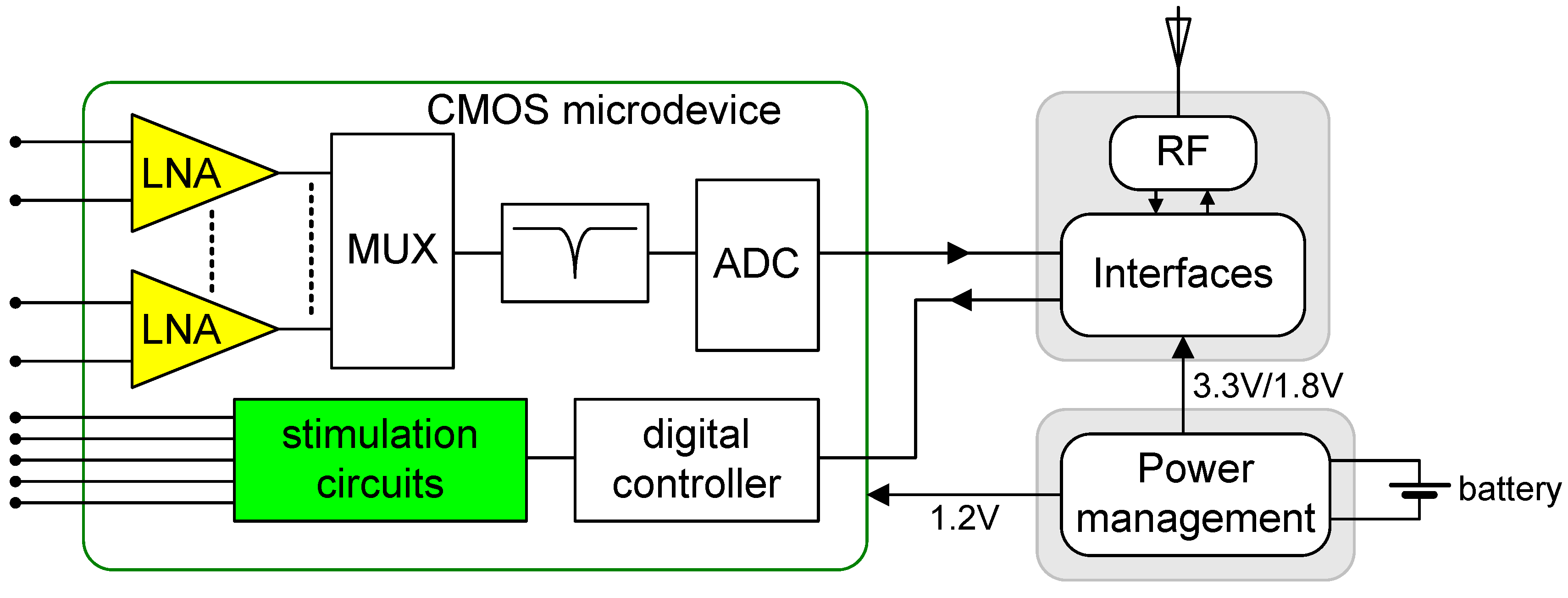
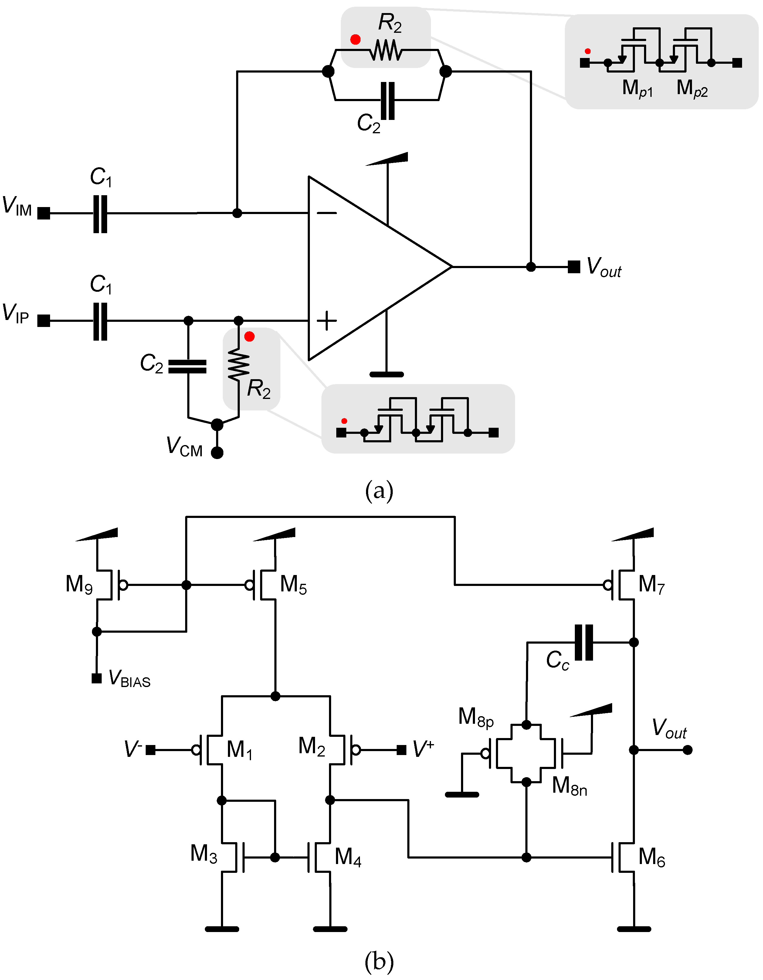


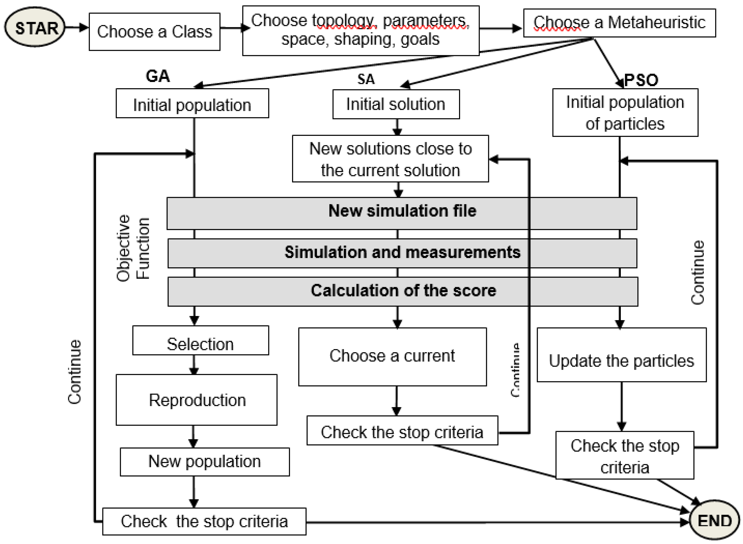
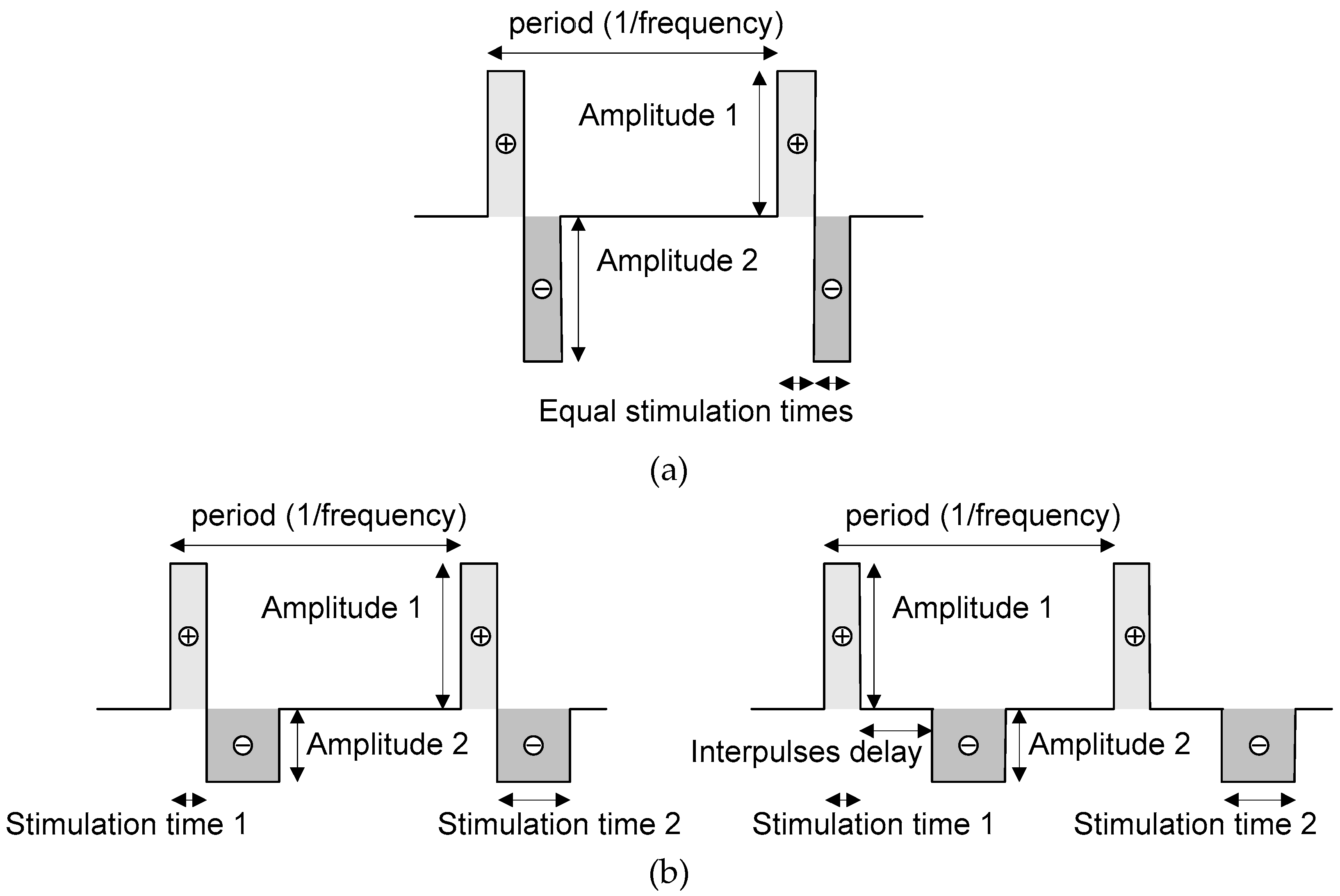
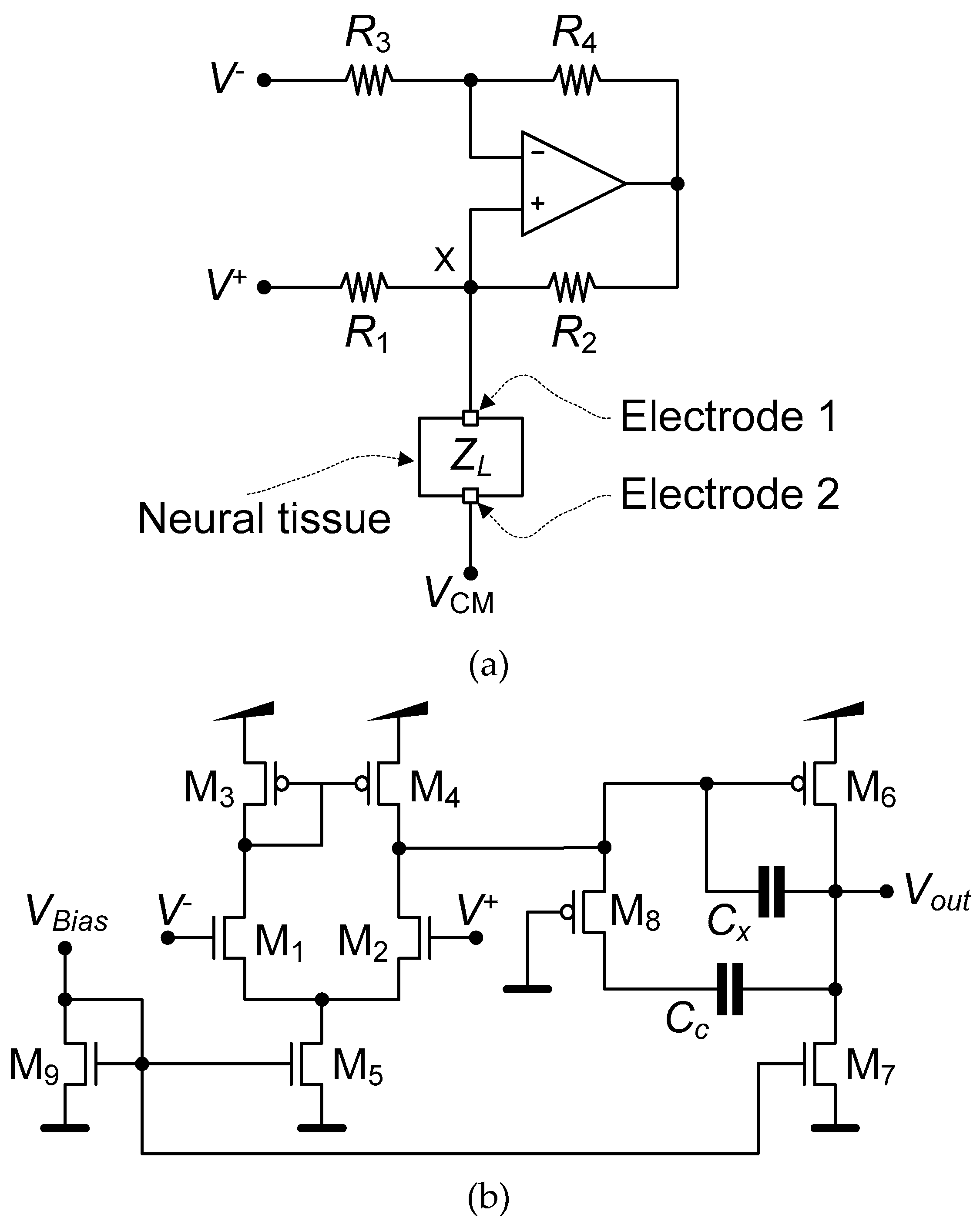
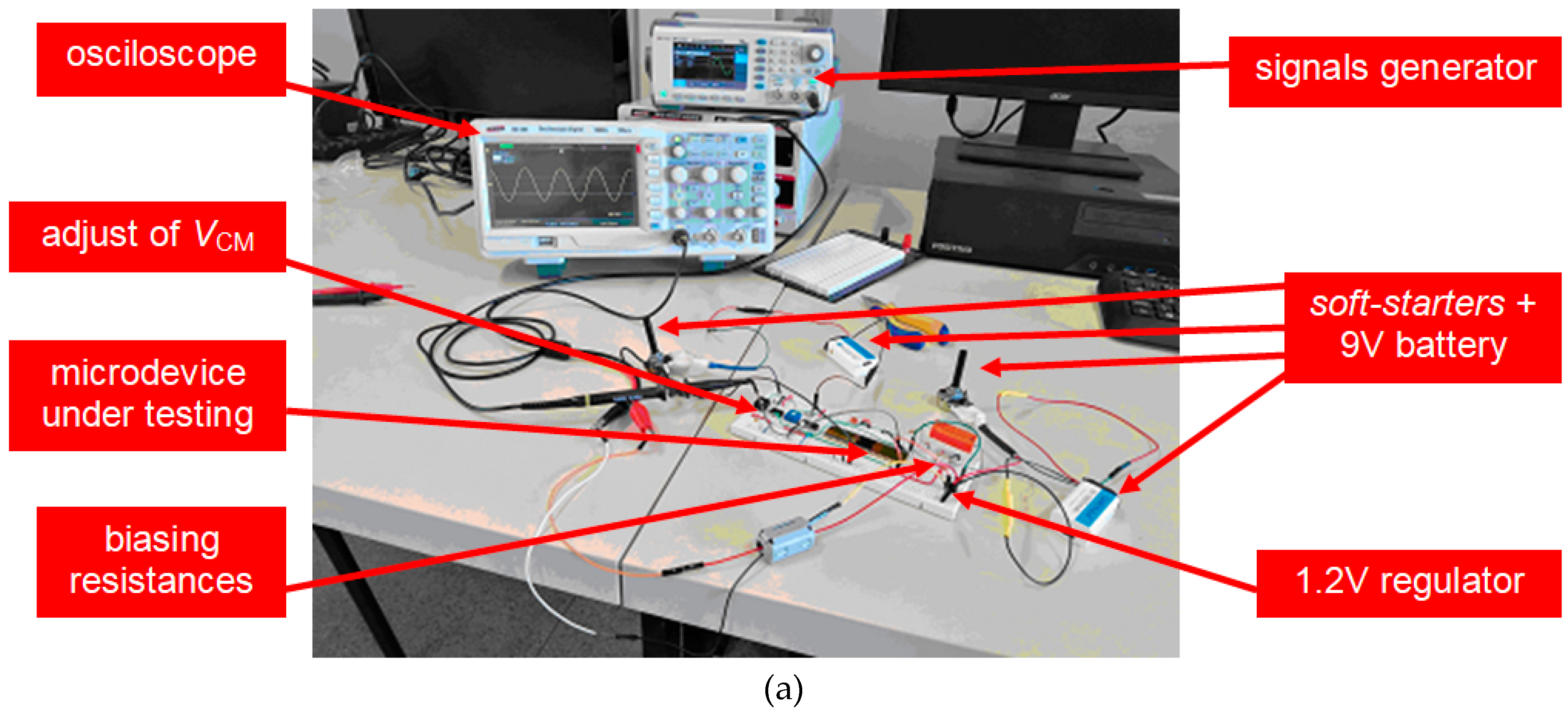
| Characteristics | Value tt |
Value ss |
Value ff |
Value sf |
Value fs |
|---|---|---|---|---|---|
| OpAmp | |||||
| Differential gain [dB] | 76.6 | 76.7 | 75.1 | 76.2 | 76.9 |
| Common Mode Rejection Rate [dB] (CMRR) | 72.8 | 71.1 | 70.4 | 74.7 | 70.9 |
| Power Supply Rejection Rate [dB] (PSRR) | 71.7 | 69 | 74 | 72.8 | 70.4 |
| Phase Margin [º] | 48 | 40 | 37 | 41 | 42 |
| Slew Rate [V/μs] | 0.138 | 0.132 | 0.145 | 0.142 | 0.134 |
| LNA | |||||
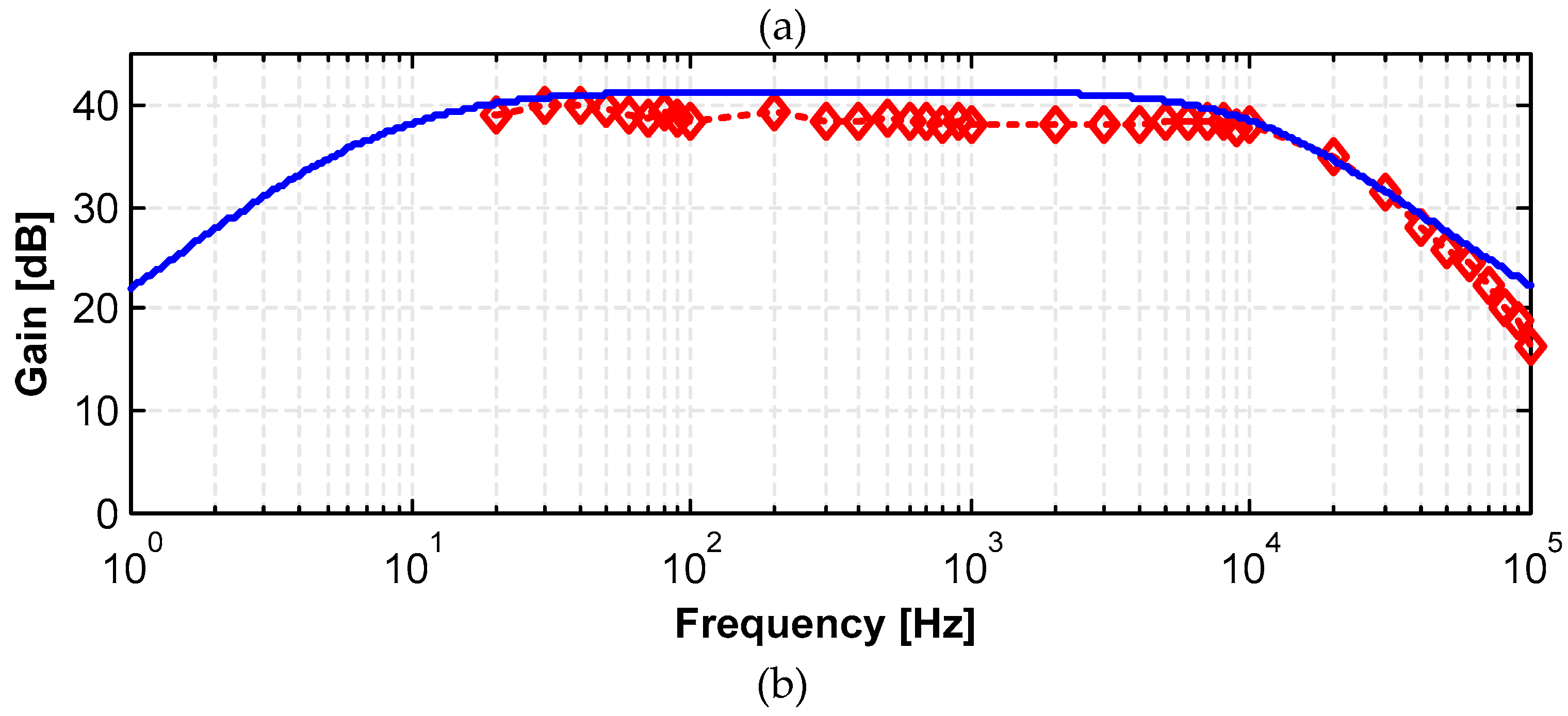
| Gain [dB] | 40.43 | 40.66 | 40.1 | 40.19 | 40.78 |
| Low cut off frequency (-3 dB) [Hz] | 19 | 13.3 | 32.6 | 24.5 | 16.3 |
| High cut off frequency (-3 dB) [kHz] | 9.0 | 8.1 | 10.1 | 9.8 | 8.1 |
| Power consumption [μW] | 6.19 | 5.85 | 6.5 | 6.4 | 5.97 |
| Input noise [μVrms] | 4.86 | 4.85 | 4.84 | 4.72 | 5.03 |
| MOSFET | Total (W/L) |
Multiplier (parallel MOSFETs) |
Fingers/multiplier | ||
|---|---|---|---|---|---|
| M1, M2 | 59 μm/0.52 μm | 2 | 10 | ||
| M3, M4 | 25 μm/14.9 μm | 2 | 1 | ||
| M5 | 48 μm/2.22 μm | 24 | 1 | ||
| M6 | 12.5 μm/14.9 μm | 1 | 1 | ||
| M7 | 12 μm/2.22 μm | 6 | 1 | ||
| M8n | 1.55 μm/12 μm | 1 | 1 | ||
| M8p | 3.1 μm/12 μm | 1 | 1 | ||
| M9 | 2 μm/2.22 μm | 1 | 1 | ||
| Pseudo-resistors | 12 μm/0.6 μm | 1 | 1 | ||
| Capacitor | Total value | Type | Sub-capacitor size | Nr. of sub-capacitors | |
| Cc | 7.5 pF | MIMcap | 10 μm × 10 μm | 36 (6 × 6 array) | |
| MOSFET | Total (W/L) |
Multiplier (parallel MOSFETs) |
Fingers/multiplier | |
|---|---|---|---|---|
| M1, M2 | 14.8 μm/0.24 μm | 2 | 1 | |
| M3, M4 | 4.68 μm/0.18 μm | 2 | 2 | |
| M5 | 14.4 μm/0.36 μm | 1 | 10 | |
| M6 | 18.72 μm/0.18 μm | 2 | 6 | |
| M7 | 28.8 μm/0.36 μm | 2 | 10 | |
| M9 | 0.80 μm/0.36 μm | 1 | 1 | |
| MOSFET |
Total (W/L) |
Number of MOSFETs in series with common gate connections | Fingers/each series multiplier | |
| M8 | 0.51 μm/7.2 μm | 4 | 1 | |
| Capacitor | Total value | Type | Sub-capacitor size | Nr. of sub-capacitors |
| Cc | 2.5 pF | MIMcap | 10 μm × 10 μm | 12 (4 × 3 parallel array) |
| Cx | 417.2 fF | MIMcap | 10 μm × 10 μm | 2 (2 × 1 parallel array) |
| Resistor | Total value | Type | Nr. of sub-resistors | |
| R1, R2 | ≈3.52 kΩ | P+ poly resistor without salicide (rppolyw0), R?≈690 Ω | Parallel of 2 series, each series composed by 2 subresistors of ≈3.52 kΩ | |
| R3, R4 | ≈24.61 kΩ | Parallel of 2 series, each series composed by 2 subresistors of ≈24.61 kΩ | ||
| Vin [mVpp] | VCM [V] | VCM,out [V] | Gmax [dB] |
|---|---|---|---|
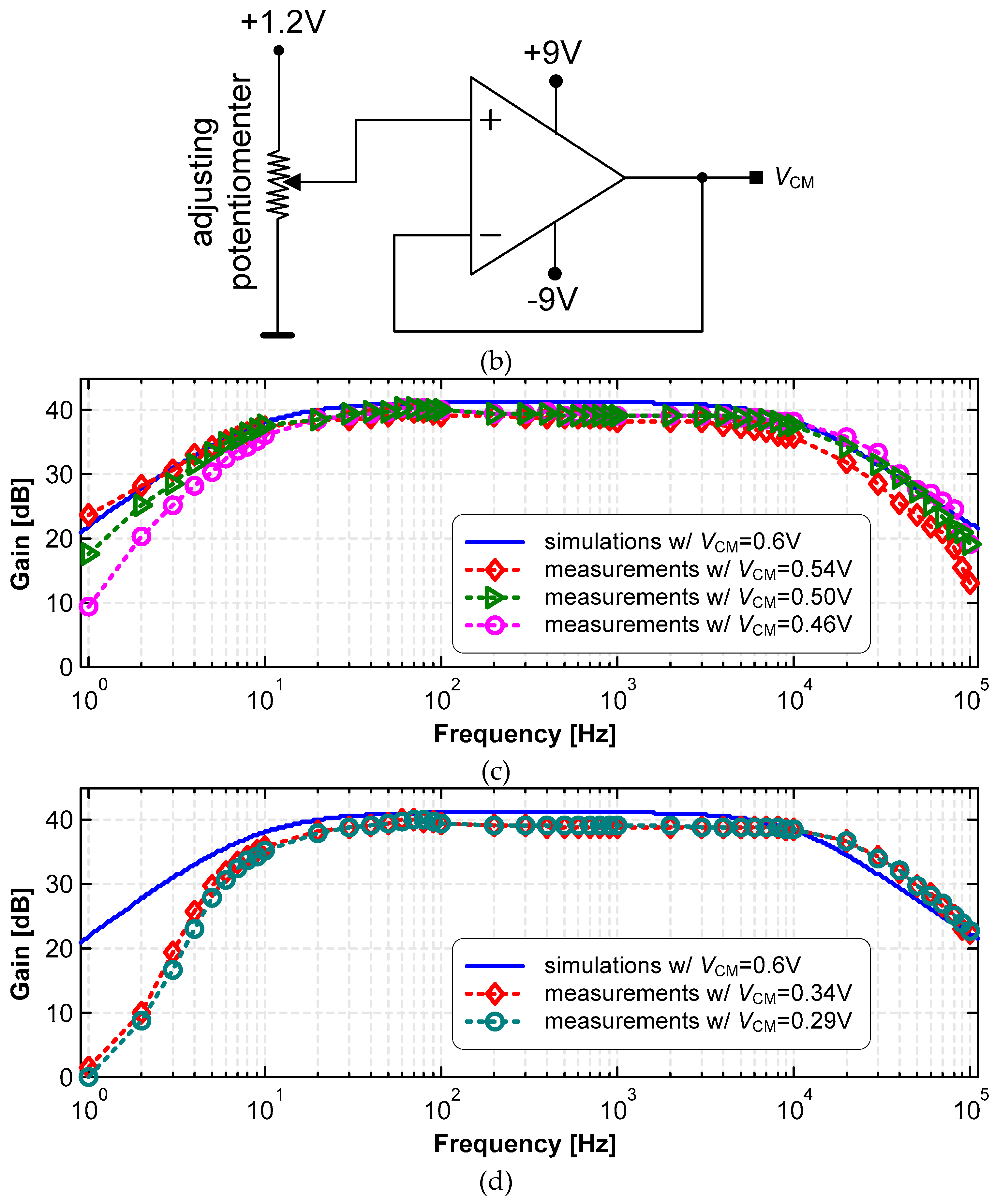
| 2 | 0.54 | 0.92 | 40.0 |
| 0.50 | 0.6 | 40.6 | |
| 0.46 | 0.53 | 40.6 | |
| 10 | 0.34 | 0.6 | 40.1 |
| 0.29 | 0.63 | 40.2 |
| Ref. | CMOS process | Mid-Band Gain [dB] | Bandwidth [Hz] | Power Supply [V] |
Power Consup. [μW] |
Area [mm2] | IRN [μVrms] | FOM [kHz/(μVrms.μW)] |
|---|---|---|---|---|---|---|---|---|
| this work+ | 65nm | 40.4 | 19 - 9k | 1.2 | 6.19 | 0.046 | 4.86 | 4.34 |
| [23] | 40nm | 25.7 | 200 - 5.0k | 1.2 | 2.8 | N/A | 5.3 | 4.40 |
| [24] | 65nm | 52.1 | 1.0 - 8.2k | 1.0 | 2.8 | 0.042 | 4.13 | 2.93 |
| [25] | 65nm | 46 | 1.0 - 10k | 0.5 | 1.5 | 0.0039 | 6.5 | 4.34 |
| [25] | 65nm | 30 | 300 - 10k | 0.5 | 2.3 | 0.025 | 5.8 | 4.76 |
| [27] | 90nm | 58.7 | 0.49 - 10.5k | 1.0 | 2.85 | 0.137 | 3.04 | 1.93 |
| [28] | 0.13μm | 40 | 0.05 - 10.5k | 1.0 | 12.1 | 0.072 | 2.2 | 2.90 |
| [29] | 0.18μm | 40 | 0.1 - 7.4k | 1.0 | 3.44 | 0.012 | 4.27 | 3.07 |
| [30] | 0.18μm | 40 | 0.05 - 7.5k | 1.2 | 4.8 | 0.022 | 3.87 | 3.44 |
| [31] | 0.5μm | 49.26 - 60.63 | 0.5 - 300 0.27-12.9k |
3.3 | 4.12 | 0.0144 | 3.16 | 2.53 |
| [32] | 0.5μm | 39.5 | 0.025 -7.2k | ±2.5 | 80 μW | 0.16 | 2.2 | 4.0 |
| Ref. | Current [μA] |
Voltage [V] | Maximum pulse frequency/ Bandwidth [Hz] |
Minimum pulse duration/ Bandwidth-1 [μs] |
Charge balance | Active charge balancing method |
|---|---|---|---|---|---|---|
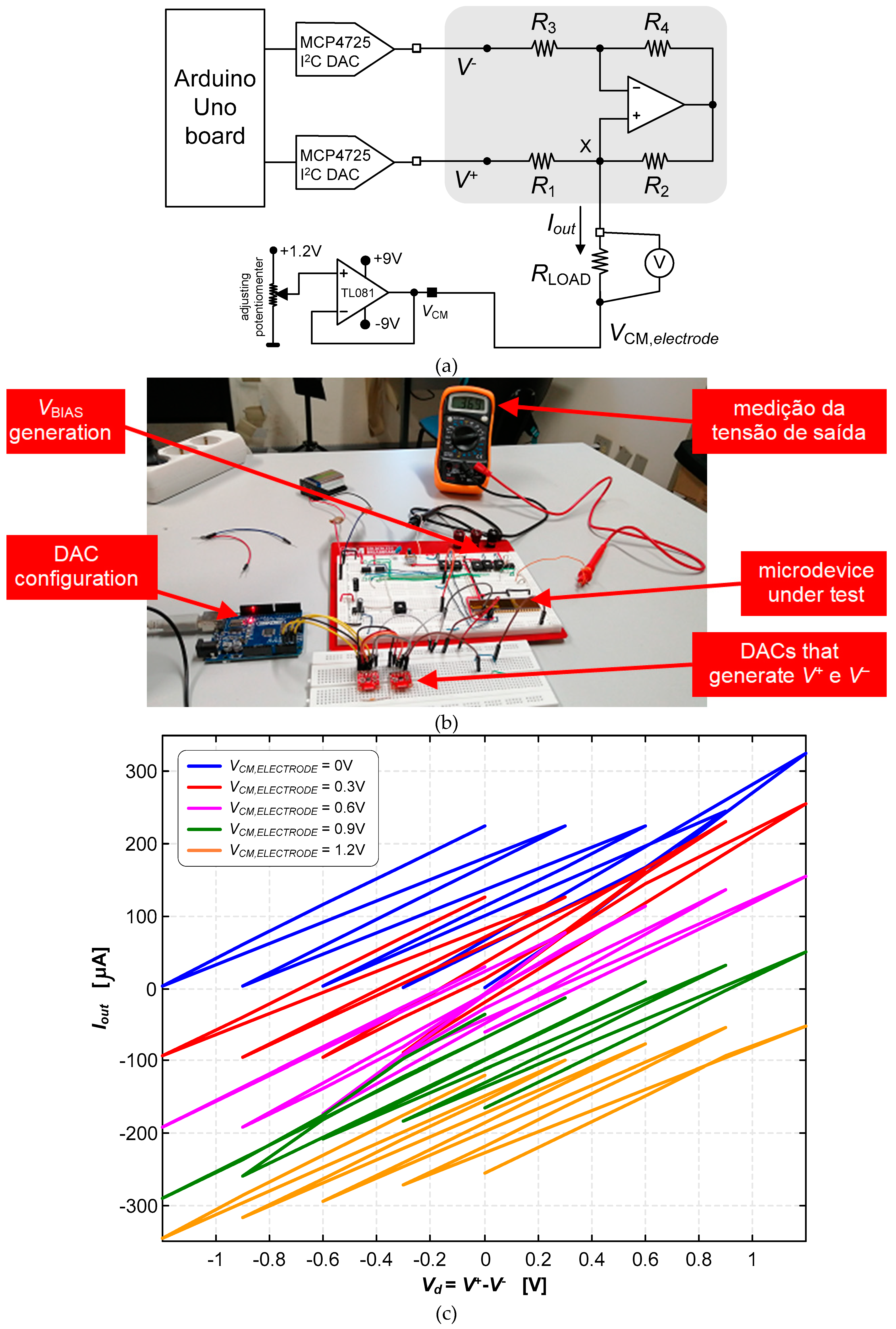
| This work | -325 to +318 | 1.2 | 1.5×10⁶ (BW) | 25 | Active | Continuous (Howland Current-Pump) |
| [42] | 20 to 2000 | 12 | 500 | 10 | Active | Switched (H-bridge) |
| [43] | -200 to +200 | 3.6 (bat) | 185 | 90 | Active | Switched |
| [44] | 0 to 200 | 3.2 (bat) | 130 | 90 | Passive | Switched |
| [45] | 30 to 1000 | 3.7 (bat) | 5000 | 10 | Active | Switched |
| [46] | -375 to +250 | 10 | 5000 | 20 | Active | Continuous (Howland Current-Pump) |
| [47] | 20 to 2000 | 4.8 (bat) | 300 | 40 | Active | Switched (H-bridge) |
| [48] | 10 to 500 | 3.1 (bat) | 200 | 60 | Passive | Switched |
Disclaimer/Publisher’s Note: The statements, opinions and data contained in all publications are solely those of the individual author(s) and contributor(s) and not of MDPI and/or the editor(s). MDPI and/or the editor(s) disclaim responsibility for any injury to people or property resulting from any ideas, methods, instructions or products referred to in the content. |
© 2024 by the authors. Licensee MDPI, Basel, Switzerland. This article is an open access article distributed under the terms and conditions of the Creative Commons Attribution (CC BY) license (https://creativecommons.org/licenses/by/4.0/).


