1. Introduction
As the transistor in circuits is increasing more and more following Moore’s law, the minimization of logic in the circuit has been an important research area for the last few decades. Many researchers are focusing on how the same function of any logic can be implemented with fewer transistors [
1,
2,
3,
4,
5]. Universal logic gates (UVM) can be a contributor to this circuit minimization technique, as they can reduce the size of circuits. Also, UVM can be used to secure the circuits by camouflaging the gates with its universal structure [
6]. In this work, we have presented the following:
We model a Function that is equivalent to a multi-function logic and represents the validity of the function.
We propose a logic gate that can implement all the basic logic gates (AND/NAND/OR/NOR/XOR/XNOR/NOT/BUF) with the same structure and less number of transistors than the regular gates.
We propose the gate using already available technology and compare the gate with previously proposed methods. We present the working principle of the proposed gate and its implementation.
2. Multi Function Logic
In this section, we formulate a generic function that can represent all the basic logic gates consisting of 2 inputs. We will use this function to model it with digital logic. Consider the function of F given below:
In this equation,
A and
are constant inputs.
X and
Y are the inputs that can have any one value from the set of {
}. We now invert function
F and get the following equation:
Simplifying Equation (
2) we will gate the expression as follows:
Equation (
3) can implement every basic 2 input gate logic depending on the values of the variables
X and
Y. We will explain how we can get all the logic gates implemented with this equation depending on the value of
X and
Y. For
X and
Y there are 4 possible values to for implementing all the logic gates truth table. We have total of 16 combinations for the values of
X and
Y. From these values, we can actually choose 8 different combinations to implement all the logic gates.
2.1. Implementation of Logic Gates
In Equation (
3) we have two variables X and Y. As we mentioned earlier there are 4 options {
} from which we can choose the value of
X and
Y. Following are the values which we need to replace in Equation (
3) to get the required logic gates:
To show an implementation if we replace the
gate value of
X and
Y in Equation (
3), we get the following:
This is basically the result of an gate. Similarly, we can implement gate as below:
This represents the implementation of the
gate. If we replace all the values according to the respective gates in Equation (
3) we will get the Boolean function of each 2 input logic gates. With this information now if we can think of a way to implement a structure that can implement Equation (
2) or Equation (
3), that will give us a multi-function gate that can implement any of the base logic gates.
2.2. Gate Level Modeling of the Multi-Function Logic
To implement the multi-function logic described with Equation (
2) or Equation (
3) can be represented in the gate-level design of logic. We can call this the modeling of the equations. In this work, we will use Equation (
2) to represent the multi function logic.
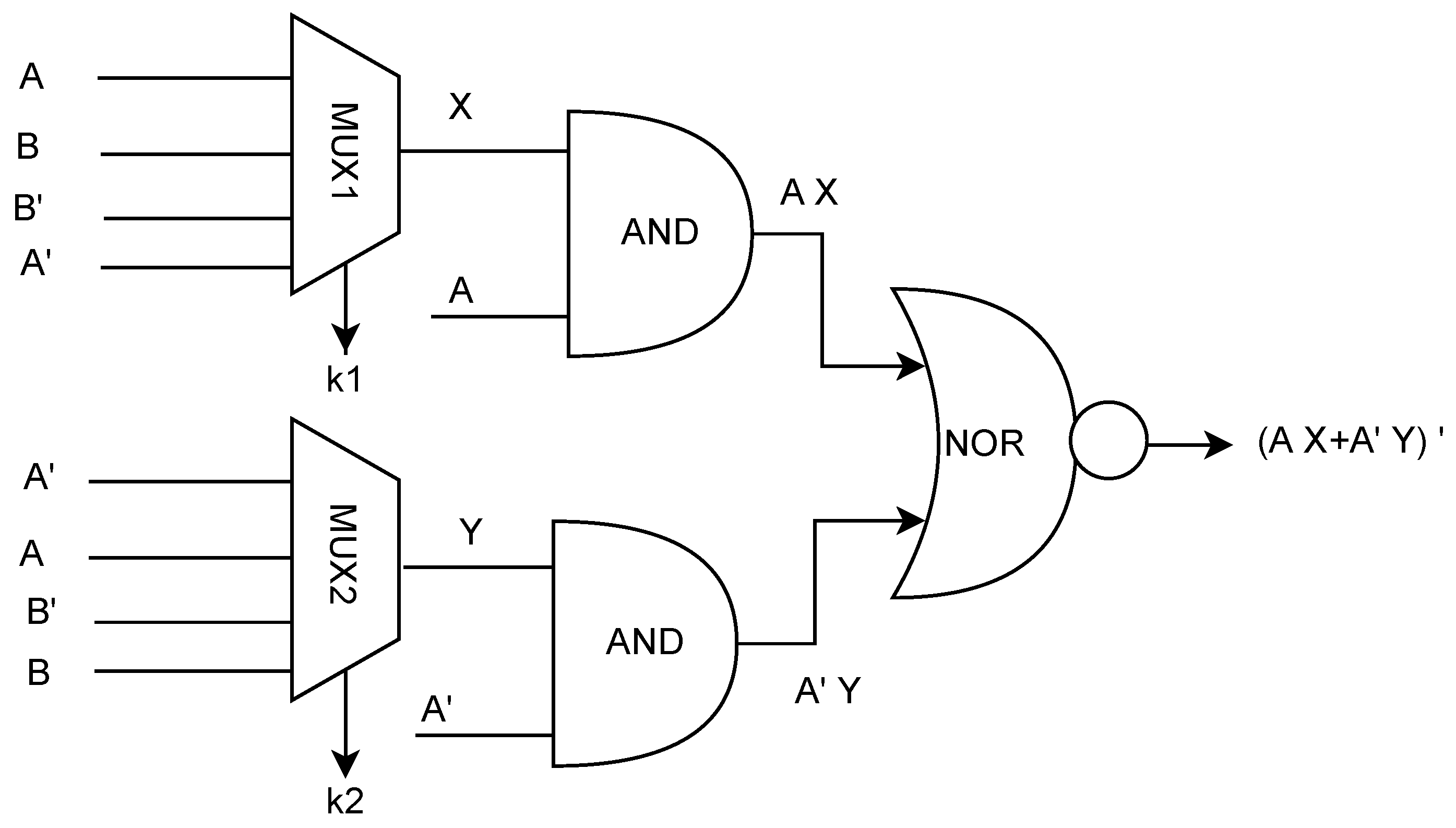
Figure 1 presents the implementation of Equation (
2) with all the options for
X and
Y in the equation.
In the figure, we can see inputs of X and Y come from a 4x1 Multiplexer which represents the choice of the input we have for both X and Y. Based on the selection of and we get the required values for X and Y.
All kinds of 2-input multi-function gates can be modeled with this equation. Based on how many functions one camouflaged gate can implement the set of the value of X and Y will be selected.
3. Gate Design
To implement a multi-function gate that has the functionality of all the logic gates we need to consider a structure that can implement these all with minimum transistors. For implementing Equation (
2) we needed to consider a structure that can give all the outputs from the same structure depending on the input. For various input options, we can consider the dummy contact-based structure which has been already implemented in various research papers. We will replace the multiplexer of the gate model with the dummy contact-based connections.
Now to implement Equation (
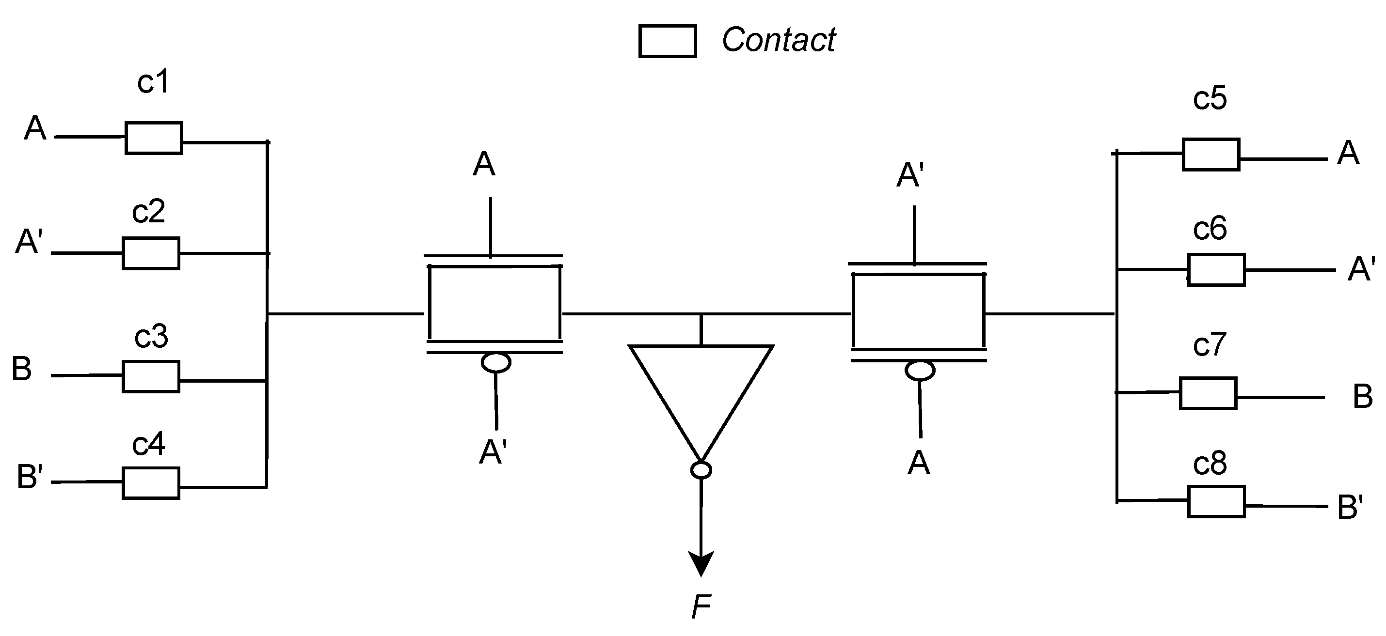
2) we design a structure based on pass transistor logic. The structure is given in
Figure 2. In
Table 1 we have represented the contacts that are needed to implement individual gates. There are 8 possible gates possible with this structure. The earlier dummy contact-based camouflage gates had to use lots of transistors to get different logic implementations with the same structure and also achieving all 8 logic gates with the same amount of transistors was not implemented with the same number of transistor connections. The structure we used is a very common structure of pass transistor logic with an inverted output and with some separating logic gate terminals. With this very easy structure, we can implement all the logic gates having 2 inputs.
3.1. Implementation of the Basic Gates
To explain the gate function we will discuss the implementation of some of the gates with the proposed pass transistor base structure. First, if we see the combination required for
gate from
Table 1 we will get the structure given in
Figure 1. If we make the truth table for the structure we will see it implements the logic for
gate. Similarly, if we also look at the combinations they will implement the other logic gates. The basis of this kind of gate structure is passed transistor-based logic. With the correct combination, we can implement all kinds of gates. The contacts which are not required for any gate will be a dummy contact and will have no effect on the gate logic.
If we take the inputs of this gate as per
Table 1 and check with the correspondent gates truth table we will see this structure satisfies the logic gates truth table.
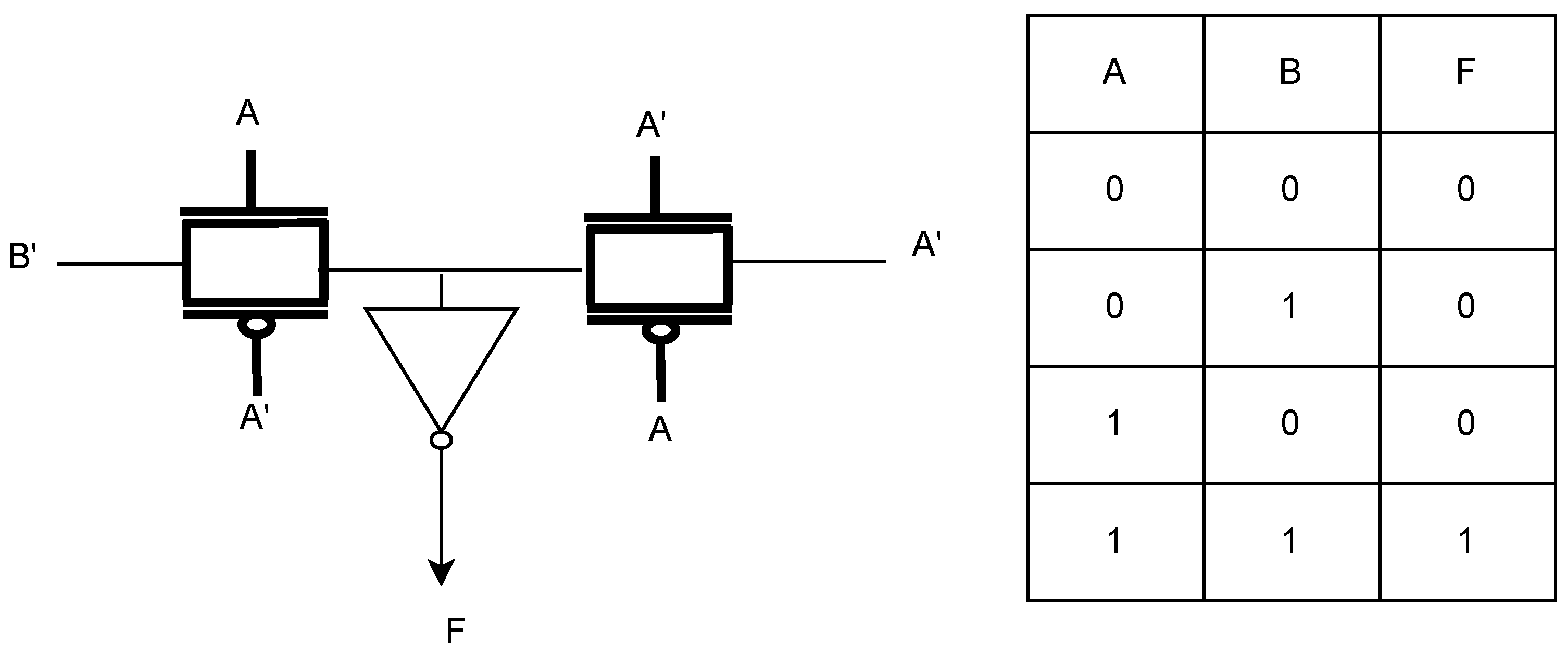
Figure 3 shows an implementation of the
gate and the truth table of its implementation. We can see the value of
F in the truth table is following the output of
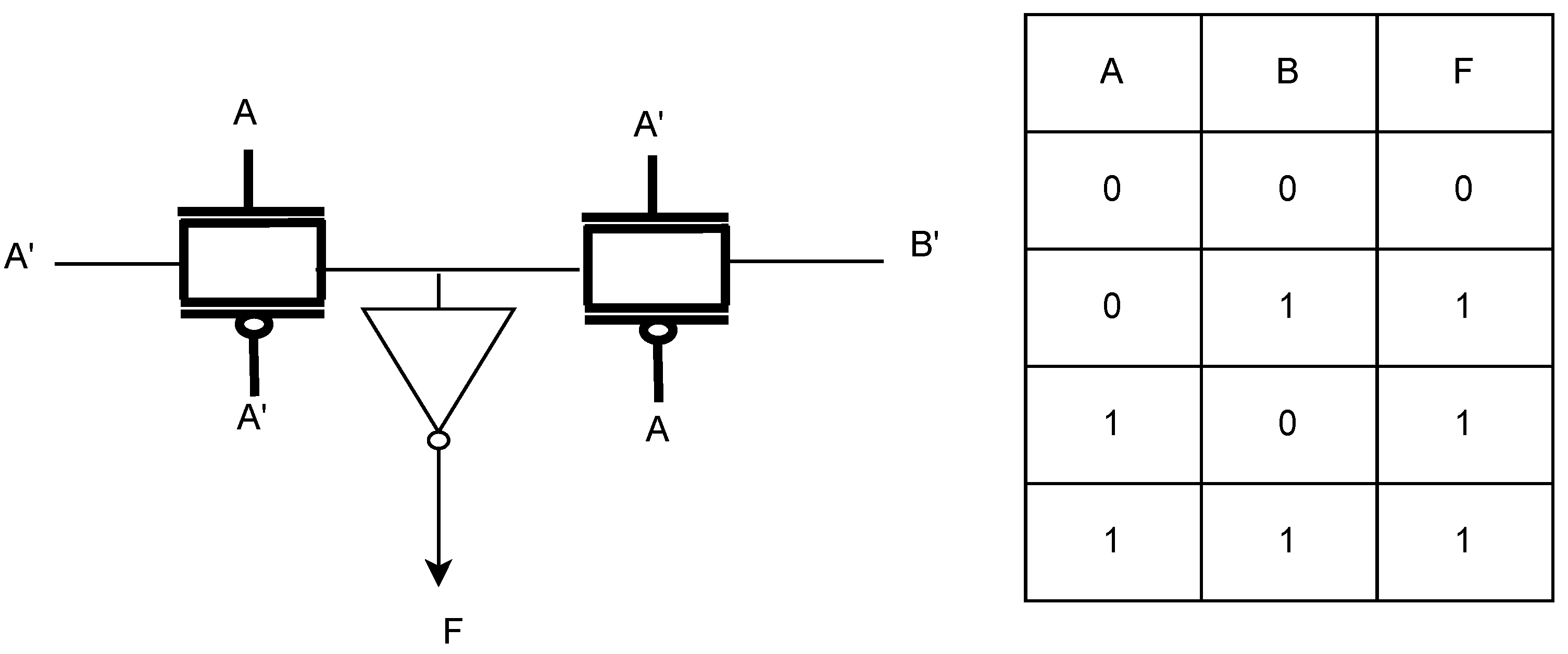
gate. Similarly
Figure 4 and
Figure 5 shows the implementation of
and
.
3.2. Spice Simulation
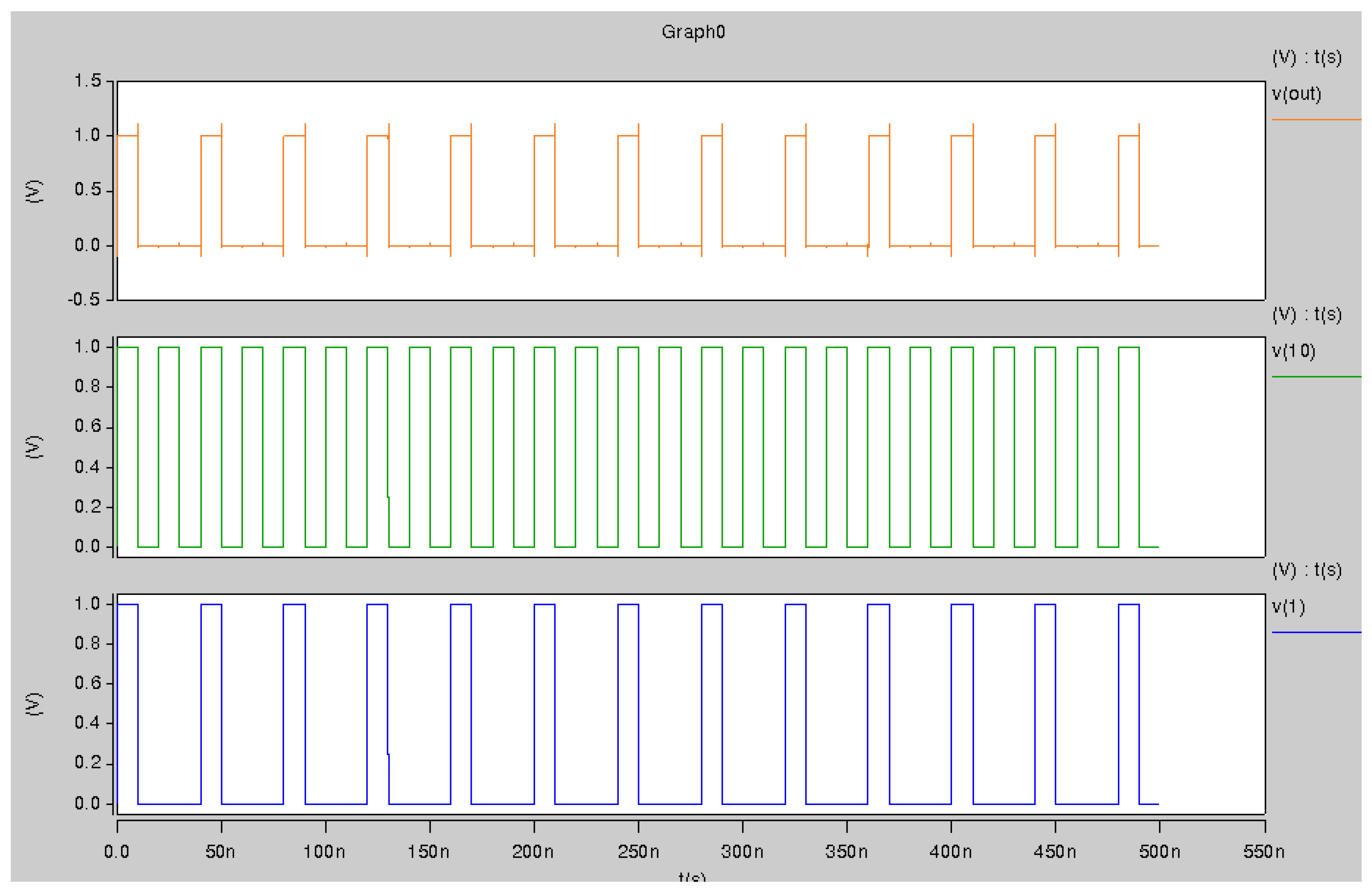
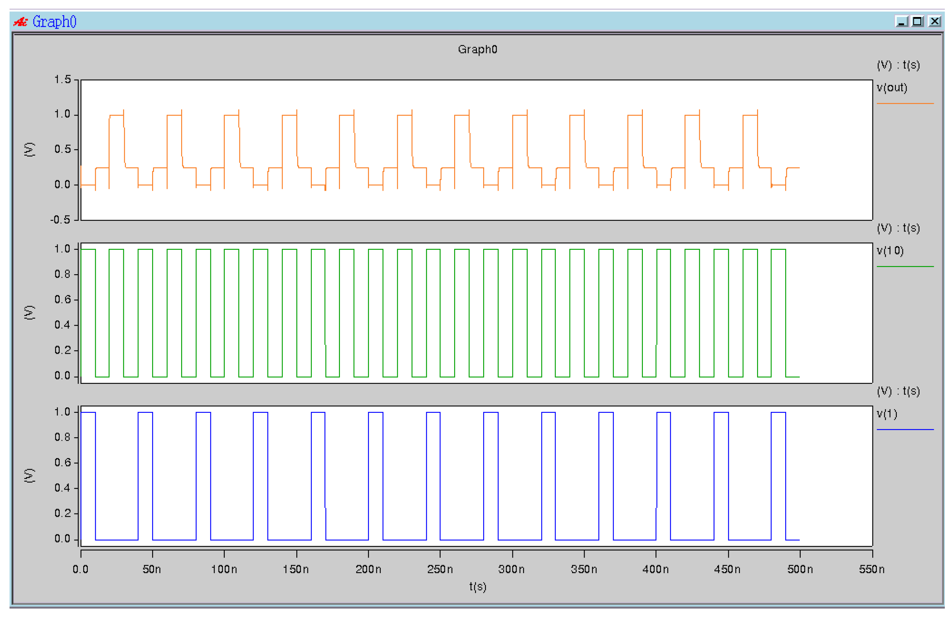
To test the correctness of the output from the proposed gate we simulated the gate in Spice and tested the outputs for different gates. We will present the output from the spice simulation in this part of the paper.
Figure 6 and
Figure 7 show the output of the hspice simulation of the
and
structure.
4. Conclusions
In this study, we showed how to design a universal gate using the pass transistor. We showed how to model the circuit with logic gates and then propose the design with pass transistor. The spice simulation output of every gate implementation has been provided. The simulations showed the implementation of the logic gates were successful with the design.
References
- Rohit Lorenzo and Saurabh Chaudhury. Review of circuit level leakage minimization techniques in cmos vlsi circuits. IETE Tech. Rev. 2017, 34, 65–187. [CrossRef]
- Rajesh Kumar Datta. Implementing boolean functions with switching lattice networks, 2022. [CrossRef]
- Rajesh Kumar Datta. Verification of crossbar-based lattice through modeling technique, 2023. [CrossRef]
- Rajesh Datta. Cvm: Crossbar-based circuit verification through modeling. 2023. [CrossRef]
- Ithihasa Reddy Nirmala, Deepak Vontela, Swaroop Ghosh, and Anirudh Iyengar. A novel threshold voltage defined switch for circuit camouflaging. In Proceedings of the 2016 21th IEEE European Test Symposium (ETS); pp. 1–2. [CrossRef]
- Rajesh Kumar Datta. Thesis Approval. Ph.D. Thesis, Southern Illinois University Carbondale, 2021.
|
Disclaimer/Publisher’s Note: The statements, opinions and data contained in all publications are solely those of the individual author(s) and contributor(s) and not of MDPI and/or the editor(s). MDPI and/or the editor(s) disclaim responsibility for any injury to people or property resulting from any ideas, methods, instructions or products referred to in the content. |
© 2023 by the authors. Licensee MDPI, Basel, Switzerland. This article is an open access article distributed under the terms and conditions of the Creative Commons Attribution (CC BY) license (http://creativecommons.org/licenses/by/4.0/).
