Preprint
Article
Area-Selective (Inhibited) Atomic Layer Deposition of ZnO on Si/SiO2 Using Tris(trimethylamino)methylsilane
Altmetrics
Downloads
198
Views
118
Comments
0
A peer-reviewed article of this preprint also exists.
This version is not peer-reviewed
Submitted:
26 May 2023
Posted:
30 May 2023
You are already at the latest version
Alerts
Abstract
Delayed atomic layer deposition (ALD) of ZnO, i.e., area selective (AS)-ALD, was successfully achieved on silicon wafers (Si/SiO2) terminated with tris(dimethylamino)methylsilane (TDMAMS). This resist molecule was deposited in a home-built, near atmospheric pressure, flow-through , gas-phase reactor. TDMAMS has been shown to react with Si/SiO2 in a single cycle/reaction and to drastically reduce the number of silanols that remain at the surface. ZnO was deposited in a commercial ALD system using dimethylzinc (DMZ) as the zinc precursor and H2O as the coreactant. Deposition of TDMAMS was confirmed by spectroscopic ellipsometry (SE), X-ray photoelectron spectroscopy (XPS), and wetting. ALD of ZnO, including its selectivity on TDMAMS – terminated Si/SiO2 (Si/SiO2/TDMAMS), was confirmed by in situ ellipsometry, ex situ SE, XPS, and/or high sensitivity – low energy ion scattering (HS-LEIS). The thermal stability of the TDMAMS resist layer, which is an important parameter for AS-ALD, was investigated by heating Si/SiO2/TDMAMS in air and nitrogen at 330 ºC. ALD of ZnO takes place more readily on Si/SiO2/TDMAMS heated in the air than in N2, suggesting greater damage to the surface heated in the air. To better understand the in situ ALD of ZnO, the data were also plotted as the normalized growth per cycle and to show the selectivity. Even one, short pulse of TDMAMS effectively passivates Si/SiO2. TDMAMS can be an effective small molecule inhibitor of ALD of ZnO on Si/SiO2 surfaces.
Keywords:
Subject: Chemistry and Materials Science - Surfaces, Coatings and Films
1. Introduction
The need for atomic layer control of materials in many scientific fields requires advances in fabrication processes and methods. Atomic layer deposition (ALD) is a powerful, advanced, thin film deposition technique that is based on self-terminating surface reactions.1,2 In its most common embodiment, ALD involves two self-terminating reactions that are used in an alternating fashion to (ideally) deposit up to a monolayer of a material on a surface with each ALD cycle. Between the two ALD reactions, unreacted reagent is pumped/purged away. When the half reactions are well chosen and properly implemented, ALD allows precise control over film thickness and uniformity. ALD is an example of bottom-up thin film fabrication because it is literally based on the atom-by-atom growth of thin films. Accordingly, an important advantage of ALD is the conformality of the films that are created. ALD can uniformly coat patterned/irregular surfaces that are often difficult to coat by other techniques.
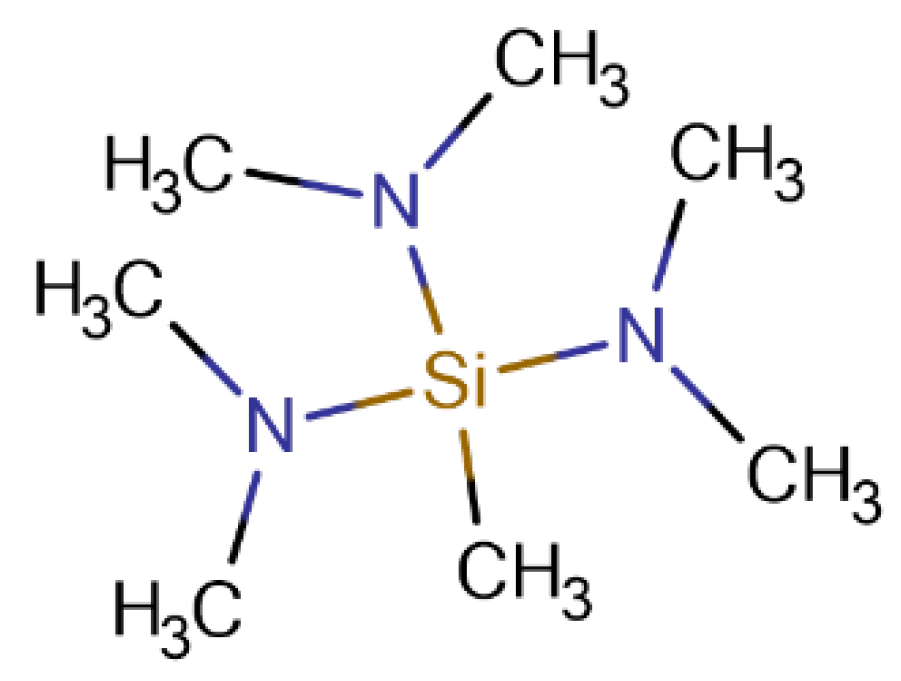
Figure 1.
The structure of tris(dimethylamino)methylsilane (TDMAMS).
Area-selective ALD (AS-ALD) is an important focus of current research in ALD.3,4 AS-ALD has also been referred to as substrate-dependent deposition.3In AS-ALD, surfaces are modified to inhibit or direct subsequent ALD growth.3,4 Thus, surface chemistry plays a central role in AS-ALD,5,6 and differences in surface chemistry can control feature sizes. There are two main approaches to AS-ALD: activation or passivation.7 However, while surface activation is a viable approach to AS-ALD, surface passivation is its core focus because it is cheaper and more scalable.8 However, there also are other AS-ALD methods such as selective precursor and co-reactant adsorption methods.9,10 Two general approaches for inhibiting a reaction at a surface are (i) to prevent a reactant’s diffusion to the active functional groups on a surface via self-assembled monolayers11 and (ii) to passivate/end-cap these groups with small inhibitor molecules.7,12 The first approach is based on sterics and the second on chemical derivatization. Although both approaches are appropriate for AS-ALD, small inhibitor/end-capping molecules often enjoy greater success because they are often both volatile and their deposition compatible with current industrial tools and processes.8
Recently, we demonstrated the surface passivation of the inner surfaces of silica capillary columns for gas chromatography using a small silane (tris(dimethylamino)methylsilane, TDMAMS) delivered by a near atmospheric pressure gas-phase reactor.13 This deposition was also followed on witness silicon shards. The reaction of surface silanols with TDMAMS was confirmed by X-ray photoelectron spectroscopy (XPS), spectroscopic ellipsometry (SE), contact angle goniometry (wetting), and high sensitivity – low energy ion scattering (HS-LEIS). HS-LEIS showed that the reaction with TDMAMS resulted in a large drop in the number of free surface silanols (from 3.66 to 0.31 silanols/nm2 on native oxide – terminated silicon). This very large decrease in the surface silanol concentration caused us to ask whether TDMAMS – terminated silicon oxide (Si/SiO2/TDMAMS) might inhibit ALD. Accordingly, we investigated the ALD of ZnO on Si/SiO2 and Si/SiO2/TDMAMS. ZnO is an important metal oxide with applications in optoelectronics, sensing, memory devices, catalysis, transparent conducting oxides, and thin-film transistors.14–18 In addition, its properties can be controlled by doping with elements such as indium (In), and gallium (Ga).19,20 In our work, ZnO was deposited by thermal ALD of diemetylzinc (DMZ) and H2O. For our surfaces, selectivity in AS-ALD can be attributed to blocking of active sites (silanols) and/or changing the reaction adsorption/desorption pathway. Furthermore, in our case, selectivity relies on the stability of the adsorbed TDMAMS. To better understand this stability, we investigated the ALD of ZnO onto Si/SiO2/TDMAMS that had been systematically damaged by heating in the air or under N2 to 330 ºC.
Selectivity in AS-ALD can be represented and displayed in different ways. For example, our data are processed/replotted here based on the normalized growth per cycle, which reveals the initial phase of growth, accelerated growth due to islanding, and steady state growth. Selectivity is also commonly represented as a selectivity window, which is the number of delayed cycles compared to growth on an uninhibited/unmodified substrate, and/or a selectivity value between 0 to 1, which correspond to no selectivity and perfect selectivity, respectively.4,21 The selectivity window can usually be determined from a plot of thicknesses versus the ALD cycle number. The second metric, the selectivity value, is based on a definition of chemical selectivity, which is derived from the underlying thermodynamics and first order kinetics of the desired and undesired surface reactions. The most common definition the selectivity, s, is the difference between the thicknesses of the films on the unmodified/unpassivated, , and modified, , substrates divided by the sum of those thicknesses (see Eq. 1).4,21,22
where , and are the amounts of deposited material on the growth and non-growth surfaces, respectively. Depending on the deposition method, θ can be calculated by different methods including scanning electron microscopy (SEM), transmission electron microscopy (TEM), atomic force microscopy (AFM), SE, or barriers/energy differences from computational studies.23 Higher selectivity is always desirable.
2. Experimental
Materials. Silicon wafers, Si(100), were obtained from University Wafer Inc. (South Boston, MA). Prior to functionalization, they were cleaned using a Basic Plasma Cleaner (115 V) from Harrick Plasma (Ithaca, NY). Tris(dimethylamino)methylsilane, TDMAMS, 97% purity, was obtained from Gelest (Morrisville, PA, USA) and used as received. Dimethylzinc (DMZ) was obtained from Strem Chemicals (Newburyport, MA, USA). HPLC grade water was used for ALD.
TDMAMS Deposition on Silicon Wafers. TDMAMS was deposited on silicon wafers at 200 °C in a previously-reported, home-built, flow-through, ambient-pressure reactor.24 Short, 20 and 30 ms, pulses of TDMAMS and water, were carried by 60 and 90 s pulses of nitrogen gas, respectively.
Atomic Layer Deposition (ALD) of ZnO on Passivated Silicon (Si/SiO2). ALD of ZnO was performed with an ALD-150LX™ system from the Kurt J. Lesker Co. (Jefferson Hills, PA) by applying 21 and 15.5 ms pulses of dimethylzinc (DMZ) and water, respectively. The purging time after each pulse was 10 s. The DMZ and water sources were held at 110 ºC and 24 ºC, respectively, and the substrate was at 200 ºC.
Ex Situ Spectroscopic Ellipsometry (SE). Ex situ SE was performed with an RC2 instrument from the J.A. Woollam Co. (Lincoln, NE, USA) from 200 to 1000 nm at three angles of incidence (65º, 70º, and 75º). The data from these measurements were modeled over the full wavelength range of the instrument to determine the thickness of the native oxide layer on silicon. Thick (7 – 8 nm) ZnO films were modeled over their (essentially) transparent region from 420 – 1000 nm using a Sellmeier model. All data modeling was in Woollam’s CompleteEASE software package (ver. 6.61 a). The ex situ SE modeling of thick ZnO reference sample was performed using a three-layer model that accounted for the silicon substrate, the silicon native oxide layer, which, again, was measured prior to deposition and fixed to the value obtained in this measurement, and a (Sellmeier) layer that accounted for the ZnO film.
In Situ Multi-Wavelength Ellipsometry. In situ SE measurements during ALD of ZnO were performed with a four-wavelength ellipsometer from Film Sense (Lincoln, NE, USA), and the data were modeled using Film Sense’s FS-1 software (Ver 2.66W).8,25,26 Two approaches were used to model the data. In the first, the optical constants for ZnO were obtained from an ex situ SE analysis of the ZnO film, which yielded values for n at 464, 523, 597, and 638 nm (the wavelengths of the Film Sense ellipsometer) to be 2.01, 2.01, 1.99 , and 1.99, respectively,27 and k was taken to be zero at these wavelengths. In the second, the ZnO film was modeled with a Sellmeier function. Both approaches produced similar thicknesses. Only the results from the first approach are shown in this work. In the modeling of the in situ data, the optical constants for heated silicon (at 200 °C) were used.
X-ray photoelectron spectroscopy (XPS). XPS spectra were acquired with a Thermo Scientific Model ESCALAB 250Xi XPS instrument equipped with a monochromatic Al K-alpha X-ray source. All XPS spectra were acquired using a focused X-ray spot size of 650 m at the sample. XPS survey spectra (0 – 1350 eV) were acquired using an analyzer pass energy of 150 eV with a 1.0 eV step size and a 10 ms dwell time. High resolution XPS spectra were acquired with an analyzer pass energy of 20 eV, a 0.1 eV step size, and a 50 ms dwell time. Charge neutralization of the samples during analysis was accomplished using a low energy electron source that is in-lens in the analyzer column plus an auxiliary combination low energy electron/low energy argon ion source in the analysis chamber. The base pressure in the analysis chamber is typically 2.0 x 10⁻⁸ mbar or better prior to XPS data acquisition. During the XPS data acquisition, the pressure in the analysis chamber is typically 2.0 x 10⁻⁷ mbar because of the low energy argon ions being leaked into the auxiliary change neutralization source.
High sensitivity-low energy ion scattering (HS-LEIS). Ion scattering experiments were performed with a Qtac100 (IonTof GmbH, Germany) instrument. Small (ca. 100 m) diameter beams of He+ (3.0 keV) were scanned over selected 2 × 2 mm2 areas. Surface charging of the samples was compensated with an electron flood gun. During the transport of the samples to the LEIS, they will pick up some (organic) contamination. Therefore, before the LEIS analyses they were cleaned with atomic oxygen (50 min). Since this may also form some ZnO2, this peroxide is converted to the regular oxide (ZnO) by annealing at 270 C. All results reported herein are based on three measurments at two different spots.
3. Results and Discussion
Passivation of native oxide – terminated silicon (Si/SiO2) with TDMAMS (Si/SiO2/TDMAMS) was confirmed by spectroscopic ellipsometry (SE), X-ray photoelectron spectroscopy (XPS), and contact angle goniometry. For SE, a simple, two-layer model accounted for the silicon substrate and the native oxide layer and was used to obtain the thickness of the native oxide layer on a plasma-cleaned silicon wafer. This same model was then used to find the combined thickness of the native oxide and TDMAMS layers. This approximation should be very good because these layers are very thin and chemically similar.28 The thickness of the SiO2 layer from the unpassivated surface was subtracted from the combined thickness of the SiO2 and TDMAMS layers on the passivated surface to yield the thickness of the TDMAMS film, which was found to be 0.54 ± 0.01 nm. The XPS Si 2p narrow scans of clean, bare Si/SiO2 before and after TDMAMS passivation are shown in Figure 2a. These narrow scans show the expected bulk Si and oxide Si 2p peaks, where evidence of the underlying spin-orbit splitting is present in the bulk Si 2p peaks.29 Consistent with the deposition of a thin film of TDMAMS on the native oxide, the ratio of the oxide Si 2p peak to the bulk Si 2p peak increases after TDMAMS deposition. Contact angle goniometry of bare Si/SiO2 and TDMAMS – modified Si/SiO2 (Si/SiO2/TDMAMS) showed that, as expected, the clean Si/SiO2 surface was wet with water, e.g., a typical water contact angle was 8°, while, after reaction with TDMAMS, the advanced water contact angle (average of three different surfaces) increased dramatically to 81.3 ± 1.5°. It is remarkable that such a thin film/layer of hydrocarbon can have such a profound influence on the wetting of a surface.
To test their ability to resist ALD, clean, bare Si/SiO2 and Si/SiO2/TDMAMS underwent 50 ALD cycles of dimethylzinc (DMZ) and water under conditions that are expected to grow ZnO. XPS shows good evidence for ZnO growth on the unpassivated surface and less growth on the passivated one. For example, after 50 ALD cycles to deposit ZnO, the Zn 2p signals from the bare Si/SiO2 are noticeably higher than those from Si/SiO2/TDMAMS (see Figure 2b). This is in a very good agreement with In addition, the Si 2p peaks from Si/SiO2 are essentially gone, which is consistent with the surface being covered with a moderately thick film of ZnO, while the Si 2p peaks from Si/SiO2/TDMAMS are still pronounced, suggesting inhibition of ZnO growth (see Figure 2c). The thickness of the ZnO film on uninhibited Si/SiO2 was measured by SEM and ex situ SE (see Experimental) to be 8 nm (see Figure 3) and 8.39 nm, respectively.
While it is often possible to determine the chemical states of elements by XPS, the Zn(0) and Zn(II) 2p3/2 peaks at 1021.4 and 1021.7 eV, respectively, are not widely spaced in energy, which makes chemical state speciation of Zn(0) or Zn(II) from this peak challenging.30 Accordingly, to confirm the chemical state of zinc in this film, we calculated its modified Auger parameter. The Auger parameter was first introduced by Wagner as the kinetic energy (KE) of a specified photoemission peak subtracted from the KE of a specified Auger peak.31,32 In many cases, it is both more sensitive to the oxidation states of elements and occurs over a wider range of energies than the positions of corresponding photoemission signals. Auger peaks are often more sensitive to sample chemistry than photoemission peaks because they involve higher energy electrons, i.e., electrons closer in energy to those used for chemical bonding. Gaarenstroom and Winogard added the photon energy to the Auger parameter, which made it independent of the x-ray energy and removed the possibility of it returning negative values.33 Their form of the Auger parameter is referred to as the modified Auger parameter. Because the modified Auger parameter is the difference between two signals, it is not generally affected by sample charging. To calculate the modified Auger parameter for Zn in our film, we found the positions of the Zn 2p3/2 and Zn LMM signals by fitting them in CasaXPS34,35 with the LA functions (see Figure 4).35,36 The modified Auger parameter was then obtained from Equation 2:
where BE stands for ‘binding energy’. The modified Auger parameter we obtained for the zinc in our film is 2010.2 eV, which is the same as that reported for ZnO, and very different for that of Zn metal/Zn(0) (2013.8 eV).37
Modified Auger parameter (eV) = BE of Zn 2p3/2 + KE of Zn LMM
To assess the inhibitory effects of TDMAMS in ALD, ALD of ZnO was followed by in situ ellipsometry on Si/SiO2/TDMAMS and bare Si/SiO2. For the unmodified surface, Figure 5a shows an induction period of slower growth over the first 5 – 10 cycles followed by steady, consistent thin film growth. In contrast, on Si/SiO2/TDMAMS, for the first 30 – 35 ALD cycles, only minimal growth of ZnO takes place. Not even 0.1 nm of ZnO has been deposited on Si/SiO2/TDMAMS after 30 DMZ-water cycles. These results suggest that TDMAMS interferes with and inhibits ALD of ZnO from DMZ and water. However, an enlarged view of the in situ ellipsometry of the ALD of ZnO on Si/SiO2/TDMAMS suggests very slow, linear growth of ZnO for the first ca. 25 ALD cycles (Figure 5b). In other words, ZnO is being slowly deposited on Si/SiO2/TDMAMS. After ca. 30 ALD cycles, ZnO deposition takes place in a more noticeable way. The results in Figure 5 showcase the value of in situ ellipsometry in ALD.
Because many ALD processes take place at higher temperatures (100 – 400 ℃), it is important that inhibited surfaces show good thermal stability. Accordingly, Si/SiO2/TDMAMS was deliberately stressed/damaged by heating to 330 °C for 20 min in an inert atmosphere (N2) or in the air prior to ALD of ZnO. Of course, exposure to the air under these conditions is expected to be more damaging. The results of ZnO growth on these surfaces are also shown in Figure 5a so that they can be directly compared to those from bare Si/SiO2 and undamaged Si/SiO2/TDMAMS. Figure 5a shows that the TDMAMS-terminated surface that was heated in nitrogen still has significant inhibitory power, although there is some suggestion that the surface has been damaged. ALD occurs somewhat earlier on this surface than on undamaged Si/SiO2/TDMAMS. In contrast, the Si/SiO2/TDMAMS surface heated in the air appears to have been substantially damaged. While ALD on this surface is initially slower than on bare Si/SiO2, it ultimately takes place quite readily. This ALD shows (i) an induction period with a low, but increasing, growth rate for ZnO, (ii) a region of rapid/accelerated film growth, which suggests the presence of islands on this surface, and finally (iii) the same steady-state growth that was observed on the unsilanized surface.21
The growth per cycle (GPC) in ALD is an important figure of merit for its performance. Figure 6a shows a representative example of how we calculated the GPC from our in situ ellipsometry results, and Figure 6b shows the GPCs for all the cycles in the deposition of DMZ and H2O on bare Si/SiO2 in Figure 5a. As shown in Figure 6b, the GPC for the ALD of ZnO on bare Si/SiO2 plateaus after 20 cycles (and maybe after 15). We define the parameter for our deposition as the average GPC at and beyond 20 cycles in Figure 6b. All the results in Figure 5a were then normalized to to yield the normalized GPCs shown in Figure 7a. This representation of the information appears to facilitate its interpretation. First, since the normalized GPCs for bare Si/SiO2 in Figure 7a were obtained from a parameter derived from the same set of data, they do not fundamentally change, except in scale. The normalized GPCs for Si/SiO2/TDMAMS that was stressed/damaged by heating to 330 °C for 20 min in the air are more interesting. They show (i) an induction period for the first ca. 18 cycles, (ii) a region of accelerated growth up to ca. cycle 32 that is indicative of island growth where the substrate surface area is higher that after island coalescence (this type of growth is commonly observed in substrate-inhibited ALD21), and (iii) a normalized GPC value for the deposition approximately equal to thereafter, which suggests that island coalescence has taken place at this point. Finally, the GPC of the Si/SiO2/TDMAMS surface that was stressed/damaged by heating to 330 °C in N2 reaches after ca. 47 cycles, while the unstressed Si/SiO2/TDMAMS surface has still not reached at 50 ALD cycles.
The traditional selectivities3 for the depositions shown in Figure 5a are presented in Figure 7b, where the threshold for selectivity (0.9) that is commonly used for comparison purposes is indicated.21 As expected, the selectivity is highest (32 cycles) for the intact TDMAMS surface. It is moderately diminished for the surface heated to 330 °C in N2 (25 cycles), and strongly diminished for the surface heated to 330 °C in the air (2 cycles). Both intact Si/SiO2/TDMAMS and Si/SiO2/TDMAMS stressed under N2 show good selectivity.
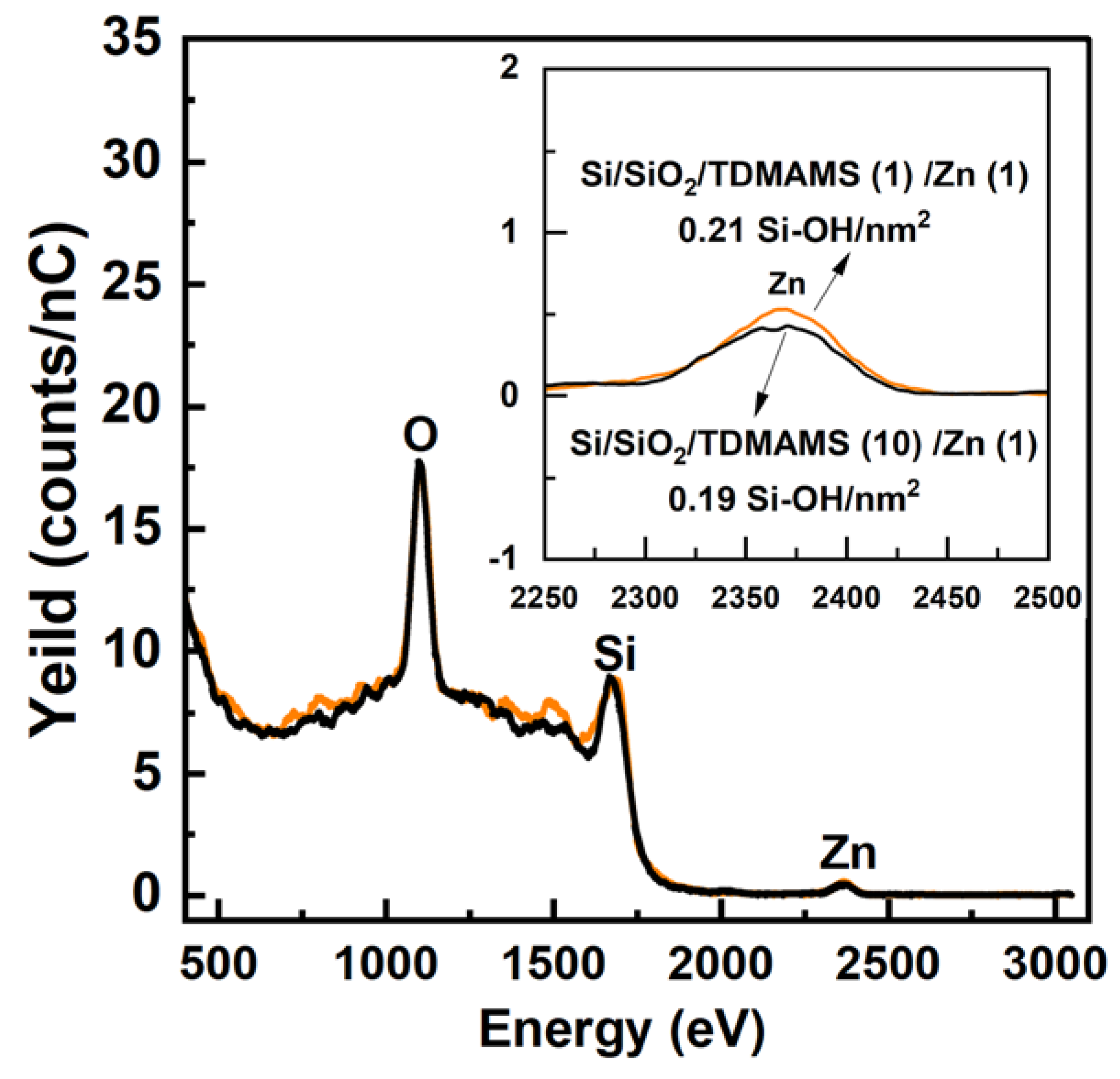
Our previous work had shown that ALD between TDMAMS and water is not possible.13 That is, previously, multiple cycles of TDMAMS and H2O did not increase the film thickness beyond what was obtained in the first deposition of TDMAMS. We followed up on these results by testing whether there was a difference in the number of silanols remaining on Si/SiO2 after exposing it to one or ten pulses of TDMAMS, where no water was applied until after the end of these pulses. After tagging these surfaces with Zn, HS-LEIS shows little difference between the number of surface silanols, i.e., Zn atoms (see Figure 8). These results confirm our previous ellipsometry measurements. Thus, one short (30 ms) pulse of TDMAMS appears to passivate Si/SiO2 almost as much as is possible with this reagent.
Conclusions
TDMAMS deposition on Si/SiO2 and ALD of ZnO on this surface were confirmed by various surface analytical techniques, including XPS, in situ and ex situ ellipsometry, wetting, and HS-LEIS. TDMAMS was stressed/heated to 330 ℃ in the air and in nitrogen. Si/SiO2/TDMAMS was not considerably damaged by heating in N2, but was seriously damaged in the air. Unstressed, TDMAMS-passivated Si/SiO2 showed a selectivity for AS-ALD of 0.9 at 32 ALD cycles. Plots of the normalized GPC facilitated the interpretation of the ALD of ZnO on TDMAMS-terminated surfaces. TDMAMS is reasonably robust and effective at preventing ALD of ZnO. Even one pulse of TDMAMS effectively passivates Si/SiO2.
Acknowledgment
This work was supported by the Restek Corporation, USA. CzechNanoLab project LM2023051 funded by MEYS CR is gratefully acknowledged for the financial support of the measurements/sample fabrication at CEITEC Nano Research Infrastructure.
References
- Puurunen, R. L. A Short History of Atomic Layer Deposition: Tuomo Suntola’s Atomic Layer Epitaxy. Chem. Vap. Depos. 2014, 20 (10-11–12), 332–344. [CrossRef]
- Kääriäinen, T.; Cameron, D.; Kääriäinen, M.-L.; Sherman, A. Atomic Layer Deposition: Principles, Characteristics, and Nanotechnology Applications; John Wiley & Sons, 2013.
- Mackus, A. J. M.; Merkx, M. J. M.; Kessels, W. M. M. From the Bottom-Up: Toward Area-Selective Atomic Layer Deposition with High Selectivity. Chem. Mater. 2019, 31 (1), 2–12. [CrossRef]
- Parsons, G. N.; Clark, R. D. Area-Selective Deposition: Fundamentals, Applications, and Future Outlook. Chem. Mater. 2020, 32 (12), 4920–4953. [CrossRef]
- Mameli, A.; Karasulu, B.; Verheijen, M. A.; Mackus, A. J. M.; Kessels, W. M. M.; Roozeboom, F. (Invited) Area-Selective Atomic Layer Deposition: Role of Surface Chemistry. ECS Trans. 2017, 80 (3), 39. [CrossRef]
- Chen, R.; Bent, S. F. Chemistry for Positive Pattern Transfer Using Area-Selective Atomic Layer Deposition. Adv. Mater. 2006, 18 (8), 1086–1090. [CrossRef]
- Mackus, A. J. M. Approaches and Opportunities for Area-Selective Atomic Layer Deposition. In 2018 International Symposium on VLSI Technology, Systems and Application (VLSI-TSA); 2018; pp 1–2. [CrossRef]
- Mameli, A.; Karasulu, B.; Verheijen, M. A.; Barcones, B.; Macco, B.; Mackus, A. J. M.; Kessels, W. M. M. E.; Roozeboom, F. Area-Selective Atomic Layer Deposition of ZnO by Area Activation Using Electron Beam-Induced Deposition. Chem. Mater. 2019, 31 (4), 1250–1257. [CrossRef]
- Weber, M. J.; Mackus, A. J. M.; Verheijen, M. A.; van der Marel, C.; Kessels, W. M. M. Supported Core/Shell Bimetallic Nanoparticles Synthesis by Atomic Layer Deposition. Chem. Mater. 2012, 24 (15), 2973–2977. [CrossRef]
- Mackus, A. J. M.; Mulders, J. J. L.; Van De Sanden, M. C. M.; Kessels, W. M. M. Local Deposition of High-Purity Pt Nanostructures by Combining Electron Beam Induced Deposition and Atomic Layer Deposition. American Institute of Physics 2010.
- Chang, C.-W.; Hsu, H.-H.; Hsu, C.-S.; Chen, J.-T. Achieving Area-Selective Atomic Layer Deposition with Fluorinated Self-Assembled Monolayers. J. Mater. Chem. C 2021, 9 (41), 14589–14595. [CrossRef]
- Xu, W.; Haeve, M. G. N.; Lemaire, P. C.; Sharma, K.; Hausmann, D. M.; Agarwal, S. Functionalization of the SiO2 Surface with Aminosilanes to Enable Area-Selective Atomic Layer Deposition of Al2O3. Langmuir 2022, 38 (2), 652–660. [CrossRef]
- Moeini, B.; Joshua W, P.; G. Avval, T.; Jacobsen, C.; Brongersma, H. H.; Prusa, S.; Bábík, P.; Vaníčková, E.; Argyle, M. D.; Strohmeier, B. R.; Jones, B.; Shollenberger, D.; Bell, D. S.; Linford, M. R. Controlling the Surface Silanol Density in Capillary Columns and Planar Silicon via the Self-Limiting Gas-Phase Deposition of Tris(Dimethylamino)Methylsilane, and Quantification of Surface Silanols after Silanization by Low Energy Ion Scattering. 2023 Submitted.
- Tonezzer, M.; Dang, T. T. Le; Bazzanella, N.; Nguyen, V. H.; Iannotta, S. Comparative Gas-Sensing Performance of 1D and 2D ZnO Nanostructures. Sensors Actuators B Chem. 2015, 220, 1152–1160. [CrossRef]
- Ding, M.; Guo, Z.; Zhou, L.; Fang, X.; Zhang, L.; Zeng, L.; Xie, L.; Zhao, H. One-Dimensional Zinc Oxide Nanomaterials for Application in High-Performance Advanced Optoelectronic Devices. Crystals 2018, 8 (5), 223.
- Sushma, C.; Girish Kumar, S. Advancements in the Zinc Oxide Nanomaterials for Efficient Photocatalysis. Chem. Pap. 2017, 71 (10), 2023–2042.
- Ellmer, K.; Klein, A.; Rech, B. Transparent Conductive Zinc Oxide: Basics and Applications in Thin Film Solar Cells. 2007.
- Hirao, T.; Furuta, M.; Furuta, H.; Matsuda, T.; Hiramatsu, T.; Hokari, H.; Yoshida, M.; Ishii, H.; Kakegawa, M. Novel Top-gate Zinc Oxide Thin-film Transistors (ZnO TFTs) for AMLCDs. J. Soc. Inf. Disp. 2007, 15 (1), 17–22.
- Guziewicz, E.; Krajewski, T. A.; Przezdziecka, E.; Korona, K. P.; Czechowski, N.; Klopotowski, L.; Terziyska, P. Zinc Oxide Grown by Atomic Layer Deposition: From Heavily n-Type to p-Type Material. Phys. status solidi 2020, 257 (2), 1900472. [CrossRef]
- Chen, M.-C.; Chang, T.-C.; Tsai, C.-T.; Huang, S.-Y.; Chen, S.-C.; Hu, C.-W.; Sze, S. M.; Tsai, M.-J. Influence of Electrode Material on the Resistive Memory Switching Property of Indium Gallium Zinc Oxide Thin Films. Appl. Phys. Lett. 2010, 96 (26), 262110.
- Parsons, G. N. Functional Model for Analysis of ALD Nucleation and Quantification of Area-Selective Deposition. J. Vac. Sci. Technol. A 2019, 37 (2), 20911. [CrossRef]
- Gladfelter, W. L. Selective Metalization by Chemical Vapor Deposition. Chem. Mater. 1993, 5 (10), 1372–1388. [CrossRef]
- Longo, R. C.; McDonnell, S.; Dick, D.; Wallace, R. M.; Chabal, Y. J.; Owen, J. H. G.; Ballard, J. B.; Randall, J. N.; Cho, K. Selectivity of Metal Oxide Atomic Layer Deposition on Hydrogen Terminated and Oxidized Si(001)-(2×1) Surface. J. Vac. Sci. Technol. B 2014, 32 (3), 03D112. [CrossRef]
- Patel, D. I.; Major, G. H.; Jacobsen, C.; Shah, D.; Strohmeier, B. R.; Shollenberger, D.; Bell, D. S.; Argyle, M. D.; Linford, M. R. Flow-Through Atmospheric Pressure-Atomic Layer Deposition Reactor for Thin-Film Deposition in Capillary Columns. Anal. Chem. 2022, 94 (21), 7483–7491. [CrossRef]
- Hilfiker, J. N. 5 - In Situ Spectroscopic Ellipsometry (SE) for Characterization of Thin Film Growth. In Woodhead Publishing Series in Electronic and Optical Materials; Koster, G., Rijnders, G. B. T.-I. S. C. of T. F. G., Eds.; Woodhead Publishing, 2011; pp 99–151. [CrossRef]
- Maynard, H. L.; Layadi, N.; Lee, J. T. C. Plasma Etching of Submicron Devices: In Situ Monitoring and Control by Multi-Wavelength Ellipsometry. Thin Solid Films 1998, 313–314, 398–405. [CrossRef]
- Fang, L.; Li, H.; Ma, X.; Song, Q.; Chen, R. Optical Properties of Ultrathin ZnO Films Fabricated by Atomic Layer Deposition. Appl. Surf. Sci. 2020, 527, 146818. [CrossRef]
- Tompkins, H. G. A User’s Guide to Ellipsometry; Courier Corporation, 2006.
- Jensen, D. S.; Kanyal, S. S.; Madaan, N.; Vail, M. A.; Dadson, A. E.; Engelhard, M. H.; Linford, M. R. Silicon (100)/SiO2 by XPS. Surf. Sci. Spectra 2013, 20 (1), 36–42. [CrossRef]
- Biesinger, M. C.; Lau, L. W. M.; Gerson, A. R.; Smart, R. S. C. Resolving Surface Chemical States in XPS Analysis of First Row Transition Metals, Oxides and Hydroxides: Sc, Ti, V, Cu and Zn. Appl. Surf. Sci. 2010, 257 (3), 887–898. [CrossRef]
- Wagner, C. D. Chemical Shifts of Auger Lines, and the Auger Parameter. Faraday Discuss. Chem. Soc. 1975, 60 (0), 291–300. [CrossRef]
- Wagner, C. D.; Joshi, A. The Auger Parameter, Its Utility and Advantages: A Review. J. Electron Spectros. Relat. Phenomena 1988, 47, 283–313. [CrossRef]
- Gaarenstroom, S. W.; Winograd, N. Initial and Final State Effects in the ESCA Spectra of Cadmium and Silver Oxides. J. Chem. Phys. 2008, 67 (8), 3500–3506. [CrossRef]
- Ortega, S.; Halicek, M.; Fabelo, H.; Callico, G. M.; Fei, B. Hyperspectral and Multispectral Imaging in Digital and Computational Pathology: A Systematic Review [Invited]. Biomed. Opt. Express 2020, 11 (6), 3195–3233. [CrossRef]
- Fairley, N.; Fernandez, V.; Richard-Plouet, M.; Guillot-Deudon, C.; Walton, J.; Smith, E.; Flahaut, D.; Greiner, M.; Biesinger, M.; Tougaard, S.; Morgan, D.; Baltrusaitis, J. Systematic and Collaborative Approach to Problem Solving Using X-Ray Photoelectron Spectroscopy. Appl. Surf. Sci. Adv. 2021, 5, 100112. [CrossRef]
- Hesse, R.; Streubel, P.; Szargan, R. Product or Sum: Comparative Tests of Voigt, and Product or Sum of Gaussian and Lorentzian Functions in the Fitting of Synthetic Voigt-Based X-Ray Photoelectron Spectra. Surf. Interface Anal. 2007, 39 (5), 381–391. [CrossRef]
- Dake, L. S.; Baer, D. R.; Zachara, J. M. Auger Parameter Measurements of Zinc Compounds Relevant to Zinc Transport in the Environment. Surf. Interface Anal. 1989, 14 (1–2), 71–75. [CrossRef]
- Collins, T. J. ImageJ for Microscopy. Biotechniques 2007, 43 (S1), S25–S30.
Figure 2.
XPS Si 2p narrow scans of (a) bare Si/SiO2 and Si/SiO2/TDMAMS, (b) The Zn 2p peaks of Si/SiO2 and Si/SiO2/TDMAMS after 50 ALD cycles of DMZ and water were applied to them, (c) The Si 2p signals from the samples in (b). In these panels, the solid orange lines correspond to bare Si/SiO2 and the dotted blue lines correspond to Si/SiO2/TDMAMS.
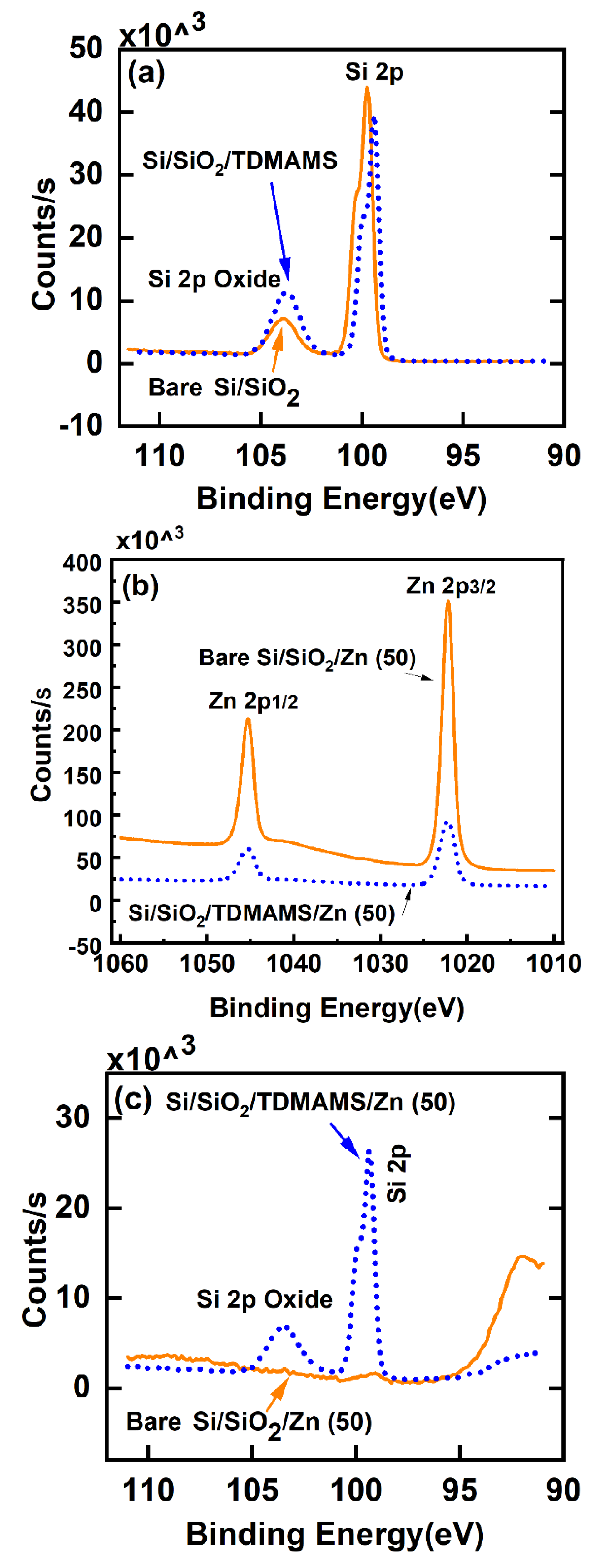
Figure 3.
SEM image of a layer of ZnO deposited on a bare Si/SiO2 substrate via 50 ALD cycles of DMZ and water. The bright region on top of the image is a protective, conductive Au/Pd/Pt coating. The contrast of this image was enhanced using the ImageJ software package.38.
Figure 3.
SEM image of a layer of ZnO deposited on a bare Si/SiO2 substrate via 50 ALD cycles of DMZ and water. The bright region on top of the image is a protective, conductive Au/Pd/Pt coating. The contrast of this image was enhanced using the ImageJ software package.38.
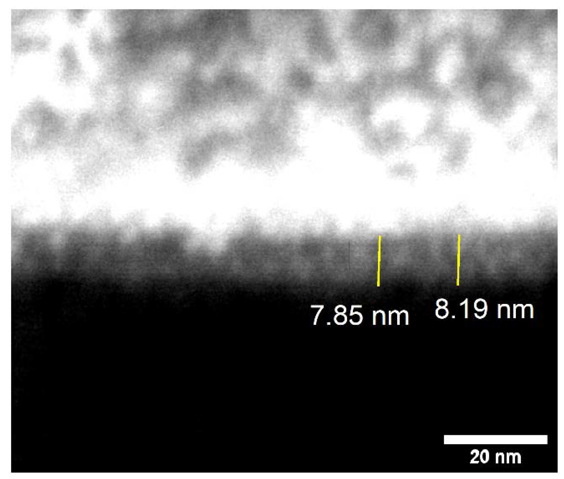
Figure 4.
XPS of ZnO deposited on a bare Si/SiO2 substrate via 50 ALD cycles of DMZ and water. (a) Narrow scan of the Zn 2p region and (b) the Zn LMM Auger signal. These signals were fit with LA functions in CasaXPS. We emphasize that these peak fits were only performed to find the positions of the maxima of the Zn 2p3/2 and Zn LMM signals from which we obtained the modified Auger parameter. We do not claim that these fits have any chemical significance.
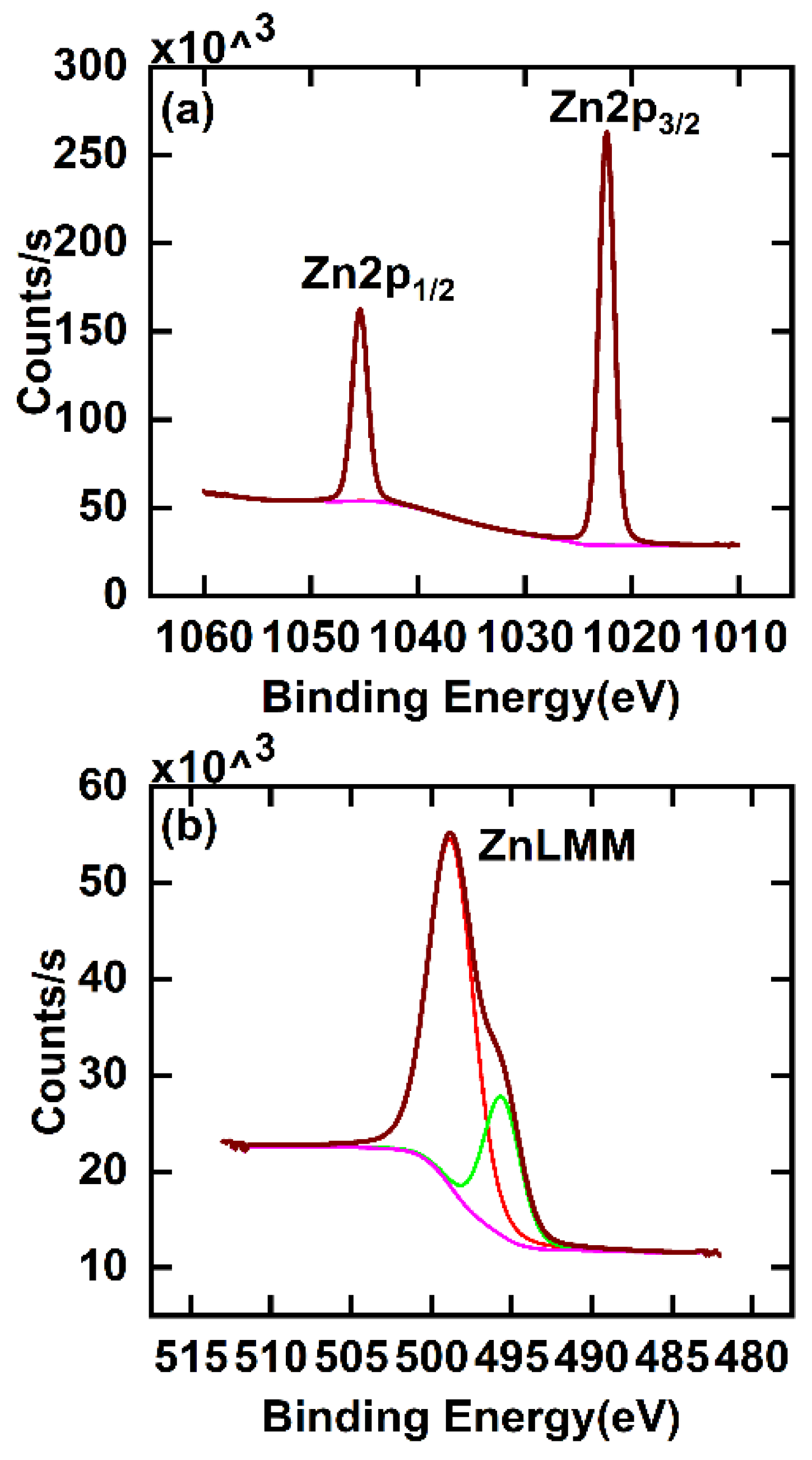
Figure 5.
In situ ellipsometry of ZnO grown by thermal ALD of DMZ and H2O on (a) bare Si/SiO2, Si/SiO2/TDMAMS, Si/SiO2/TDMAMS damaged by heating to 330 °C in N2, and Si/SiO2/TDMAMS damaged by heating to 330 °C in the air. (b) An enlarged view of the results in (a) of the in situ ellipsometry of ZnO grown by ALD on Si/SiO2/TDMAMS. The inset of this panel shows the ZnO growth for the first 25 cycles of the deposition and a linear fit to these thicknesses.
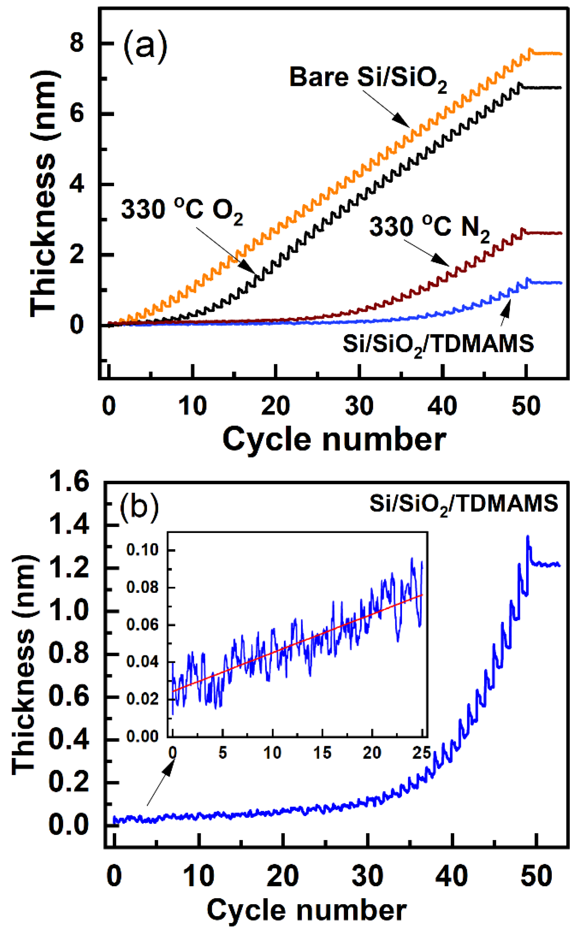
Figure 6.
(a) An enlarged view of a portion of the in situ ellipsometry results in Figure 5a for the ALD of DMZ and H2O on bare Si/SiO2 showing an example of the determination/calculation of the growth per cycle (GPC). (b) The GPCs for all the cycles in the ALD of DMZ and H2O on bare Si/SiO2. The red line through the data is a guide to the eye.
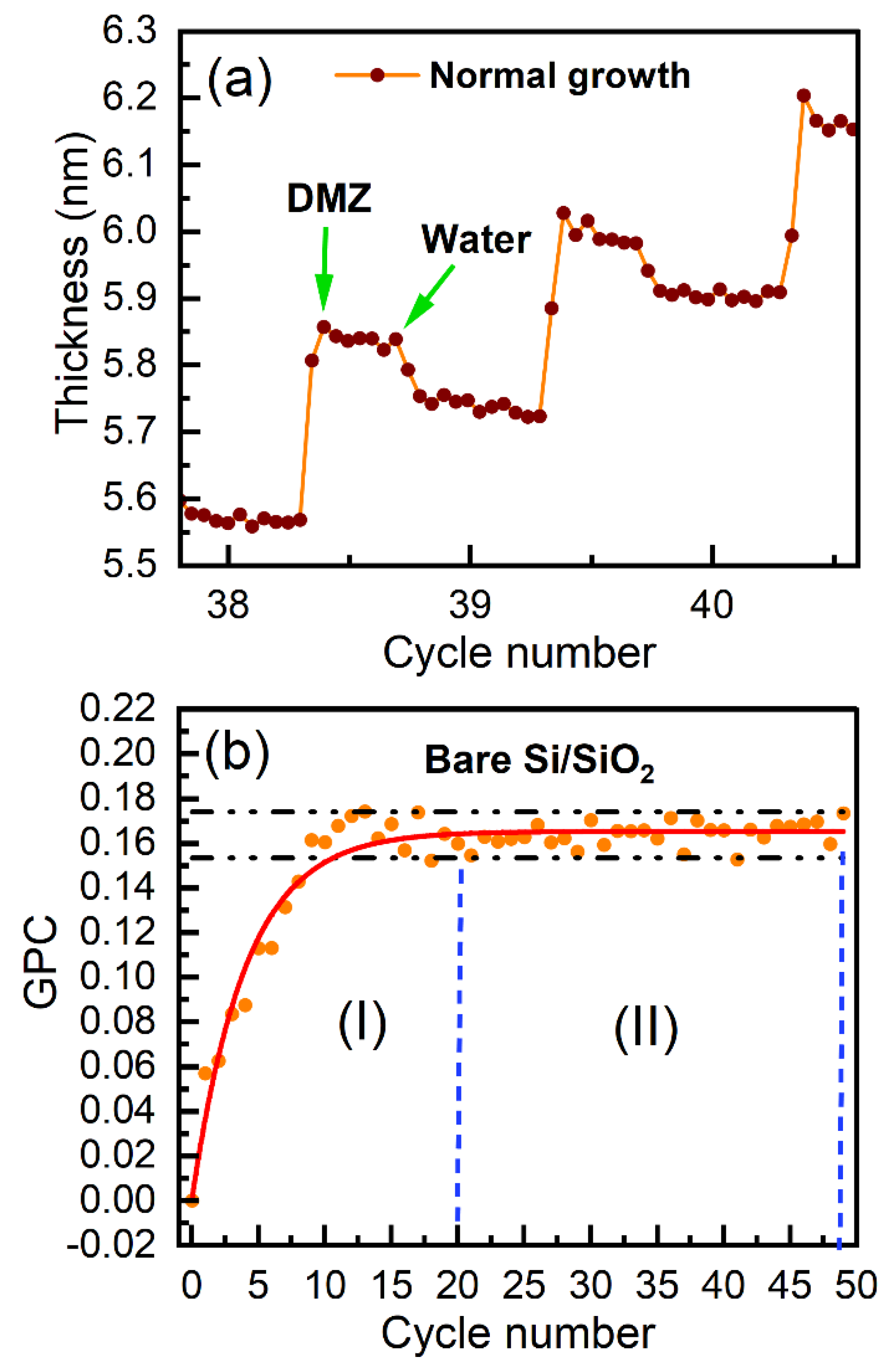
Figure 7.
(a) Normalized growth per cycle and (b) selectivities as a function of the number of ALD cycles for the ZnO ALD growth on bare Si/SiO2, Si/SiO2/TDMAMS, and Si/SiO2/TDMAMS heated to 330 °C in N2 or the air in Figure 5a.
Figure 7.
(a) Normalized growth per cycle and (b) selectivities as a function of the number of ALD cycles for the ZnO ALD growth on bare Si/SiO2, Si/SiO2/TDMAMS, and Si/SiO2/TDMAMS heated to 330 °C in N2 or the air in Figure 5a.
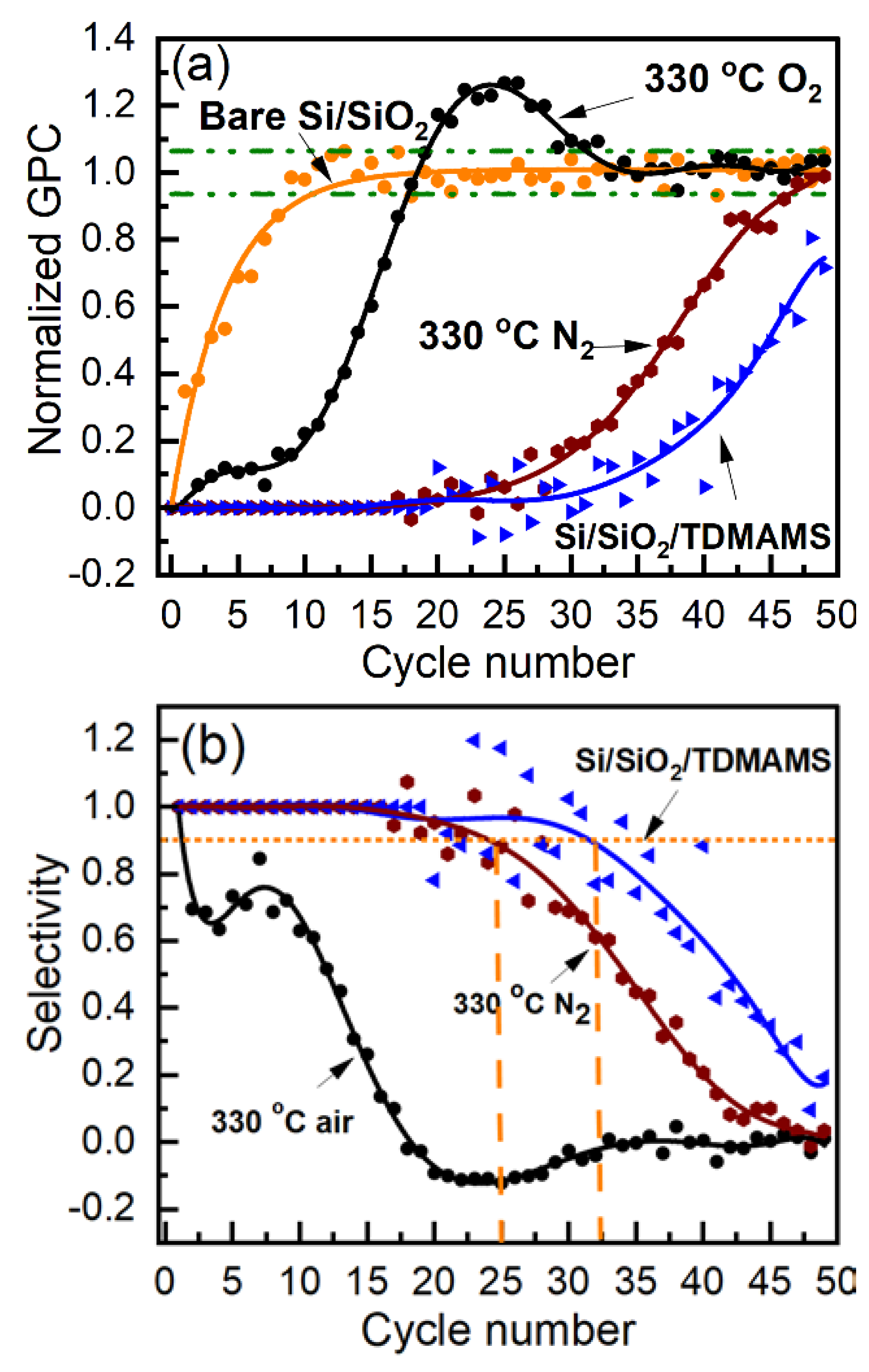
Figure 8.
LEIS spectra of Si/SiO2 passivated with one pulse of TDMAMS and then reacted with DMZ (Si/SiO2/TDMAMS(1)/Zn(1)), and Si/SiO2 passivated with ten pulses of TDMAMS and then reacted with DMZ (Si/SiO2/TDMAMS(10)/Zn(1)). The inset of this figure is an enlargement of the Zn region of the spectra shown in the main panel.
Disclaimer/Publisher’s Note: The statements, opinions and data contained in all publications are solely those of the individual author(s) and contributor(s) and not of MDPI and/or the editor(s). MDPI and/or the editor(s) disclaim responsibility for any injury to people or property resulting from any ideas, methods, instructions or products referred to in the content. |
© 2023 by the authors. Licensee MDPI, Basel, Switzerland. This article is an open access article distributed under the terms and conditions of the Creative Commons Attribution (CC BY) license (http://creativecommons.org/licenses/by/4.0/).
Copyright: This open access article is published under a Creative Commons CC BY 4.0 license, which permit the free download, distribution, and reuse, provided that the author and preprint are cited in any reuse.
MDPI Initiatives
Important Links
© 2024 MDPI (Basel, Switzerland) unless otherwise stated


