1. Introduction
In 1971, the memristor is the fourth basic circuit element that is proposed by L. O. Chua in theory [
1]. As the fourth basic circuit element besides resistor, capacitor, and inductor, memristor has been considered as one of the next generations of non-volatile memory technology. The memristor is a nonvolatile device and has variable memristance. When the current flows through the memristor from different directions, the memristance will change accordingly. When the current cross the memristor was removed, the memristance will remained. In 2008, the first physical memristor was reported by HP labs [
2]. The phenomenon of resistive switching in electronic devices has attracted wide interest from academia and industry, due to its application to store information in a memristor, enabling the development of neuromorphic and memory-centric computing systems [
3,
4,
5,
6,
7,
8,
9].
In recent years, programmable and reconfigurable analog elements have attracted considerable attention. In the literature, there have been various studies on the programmable circuit. In 2010, Pershin et al. developed a programmable memristor circuit that includes a microprocessor, analog-to-digital converter (ADC), and digital potentiometer [
10]. In 2012, Berdan et al. presented a circuit that exploited the dynamic modulation of resistance under a constant DC bias on the operation of an analog programming circuit for accurately setting the state of a memristor [
11].In 2016, Merced et al. investigated memristor 1T1R arrays rapidly reaching arbitrary conductance states and programming was performed by applying an adaptive pulsed algorithm that utilized the transistor gate voltage to control the SET switching operation [
12]. Kim et al. suggested an interesting tuning approach that is to exploit the voltage divider (VD) effect and its HW simplicity via a resistor in series with the memristor [
13,
14,
15]. In 2017, Olumodeji et al. presented a circuit for accurately programming the memristor in both an incremental and a decremental fashion using auto-tuning operational amplifier's gain, which exploited the characteristics of the memristor, and this circuit took advantage of the memristor's pulse-based programmability [
16]. Mokhtar et al. presented a pulse-coded memristor programming method adopted in RWC (resistance writing circuit) design. It used 2 sets of switches to decrease or increase memristance by supplying a positive or negative pulse [
17]. In 2020, Tarkhan et al. presented a novel CMOS circuit for programming memristors which used a Wheatstone bridge circuit to measure the current memristance while the programming current was flowing through the device [
18]. In 2022, Knowm Inc. explored different circuit topologies and approaches to perform the forming of RRAM and a target-resistance was pursued through pulsed voltage stress, followed by cycle-to-cycle stabilization using a custom trans-impedance amplifier circuit [
19]. In 2022, Lu et al. analyzed the reason of the resistance state deviation of the memristor by studing predecessors on read and write circuit, and proposed a novel structure of memristor based on opposite polarity [
20]. In 2023, Randrianantenaina et al. reported programmable and reconfigurable analog/digital platforms as an alternative perspective in order to promote analog and digital applications based on memristors [
21].
In this paper, we suggest an approach to program memristors in analog circuits based on the threshold-type behavior of the memristor. Our main idea is to use a negative source to programs the memristor to high resistance states (HRS). The positive source then programs the memristor to aim memristance. In addition, we have added a reference resistor to program the memristor to multi-level memristance according to digital input signals. Finally, a convolutional neural network (CNN) has been trained by our circuit and 77.64% classification precision can be achieved even under 22.2% memristance tolerance. In this way, we obtain a programmable circuit that can obtain accurate memristance and has a simple structure.
2. The memristor Programmable Circuit
2.1. Memristor Model
The adopted memristor model has been proposed by Pershin Y. V. [
22]. The memristor has a threshold characteristic. In other words, when the voltage applied to the memristor is greater than the threshold value, the memristance (memristor resistance) will change. Otherwise, the memristance will remains unchanged. The mathematical expressions of this model are as follows:
where
X represents n-th internal state variables, and
X is a vector.
is the voltage applied to the memristor,
I(t) is the current that flows through the memristor.
is the memristor threshold voltage.
is the memristance which is a scalar.
is the LRS and
is the HRS. The
θ(•) are step functions that are used to limit the memristance to the region between
and
. The coefficients
α and
β define the slopes of the
curve below and above the threshold, which characterize the rate of memristance change at
and
, respectively.
A positive or negative voltage applied to the memristor decreases or increases the memristance
. The device state changes only when
(for set transition
, and for reset transition
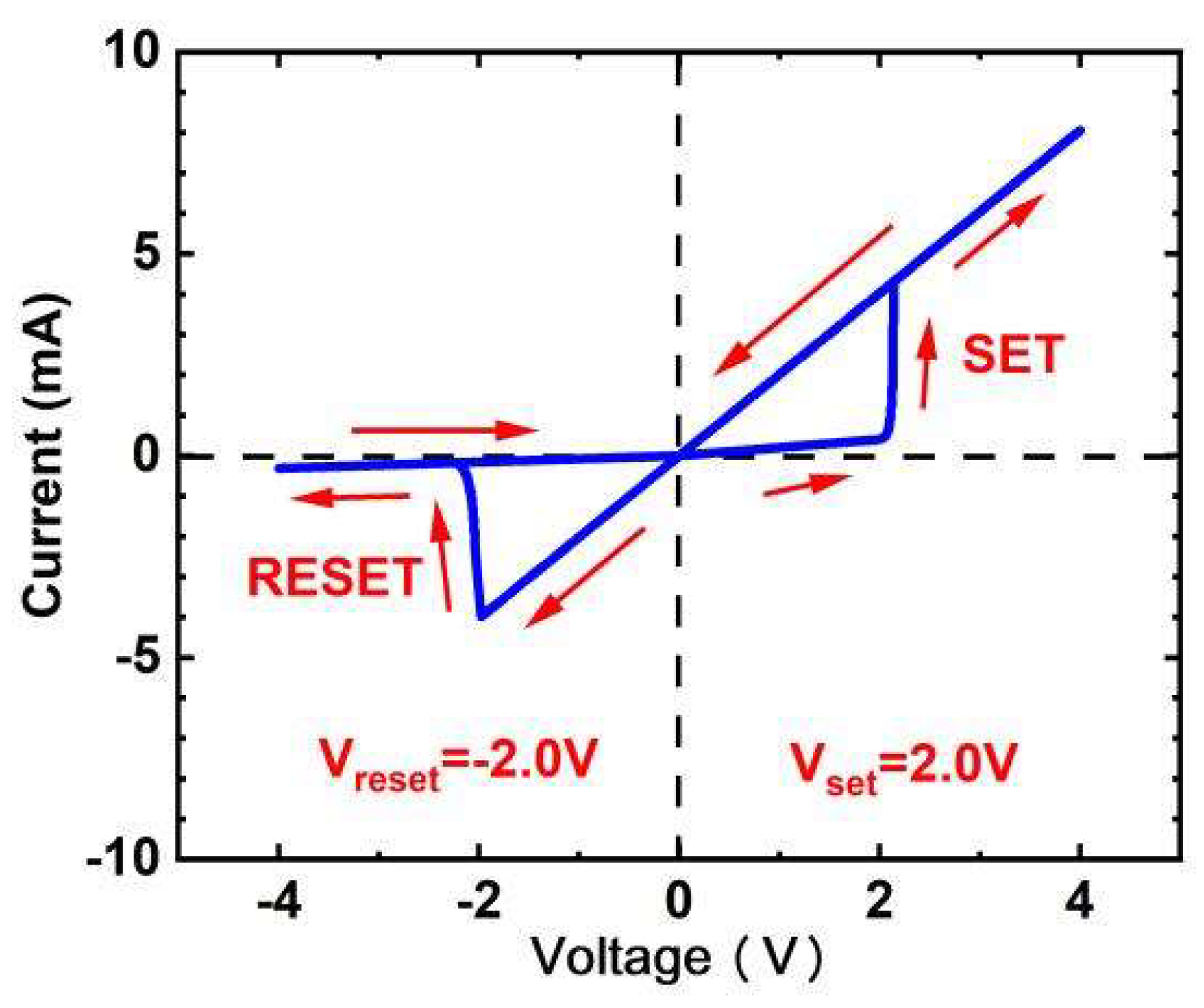
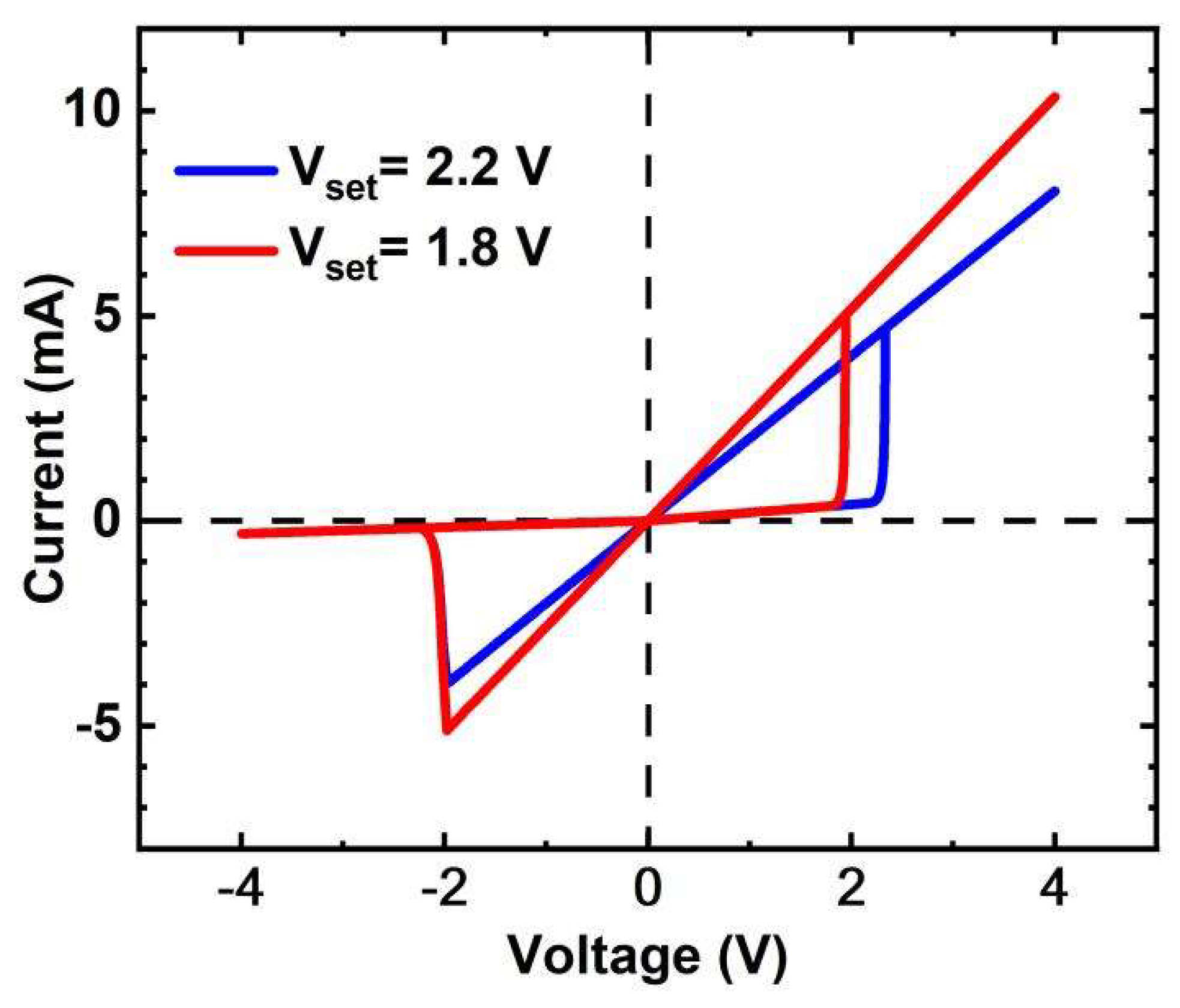
). As shown in
Figure 1., when the voltage value applied to the memristor is greater than the positive threshold of the memristor (
), the memristance decreases sharply, memristor tends to change from HRS to LRS, and the process is SET transition, when the voltage value applied to the memristor is less than the negative threshold of the memristor (
), the memristance increases sharply, memristor tends to change from LRS to HRS, and the process is RESET transition.
2.2. The Memristor Programmable Circuit
In the programmable analog circuits of memristors, Pershin et al. developed a circuit that applied negative voltage to the memristors and then use positive voltage to program the memristor's states during their operation as analog circuit elements [
10]. In addition, the voltage divider effect is usually used in programmable circuit[13‒15]. This paper proposes a novel circuit by utilizing before design ideas and adding a reference resistor that is designed to be controllable. The circuit is simple and the memristance is configurable.
When programming the memristor, if the memristance is greater than the aim value, it is necessary to decrease the memristance through a SET process. If the memristance is less than the aim value, it is necessary to increase the memristance through a RESET process. Before programming the memristor, it is first to obtain the greatest memristance value
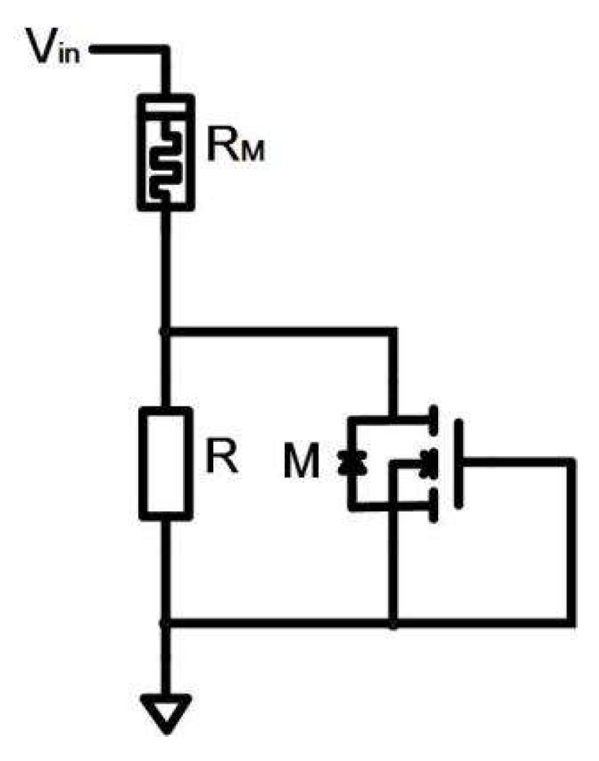
by RESET process. Then it programs the memristor to aim value. In addition, we also add a reference resistor which contributes to obtaining aim memristance, through this structure the memristance is configurable. The memristance is related to the reference resistor, and the reference resistor is controlled by digital input signals. The proposed memristor programmable circuit structure contains one memristor, one NMOS, and one reference resistor as shown in
Figure 2.
is the memristor,
R is the reference resistor, and
M is the NMOS, respectively.
The programming progress contains two steps:
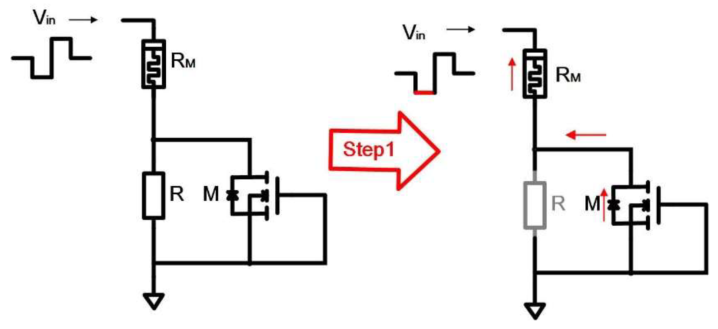
Step 1: the input source
(
) is negative. the current flows through NMOS (NMOS can be regarded as a diode) and then through memristor
to reset the memristor, as shown in
Figure 3. So, the memristance increases sharply to
.
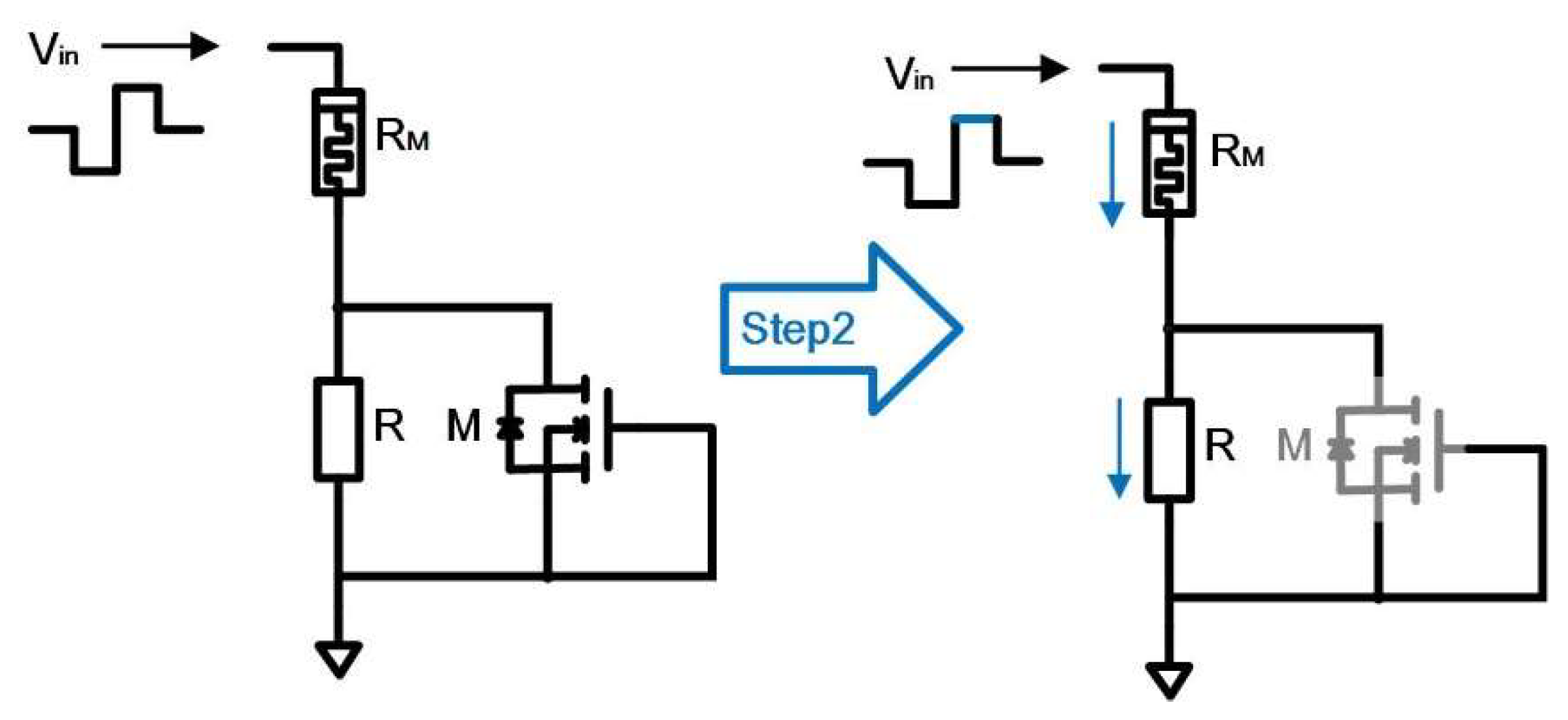
Step 2:the input source
is positive, and the current flows through memristor
and reference resistor
R (NMOS can be regarded as open), as shown in
Figure 4. The voltage applied to the memristor is positive (it must match
), and the voltage value is
when
, memristor SET, the memristance decreases gradually, and the memristor voltage value also decreases gradually, until
. When
, the memristor stops SET, so the memristance does not change and remains a certain value, the memristance value is
where
is the input source,
is the memristor SET transition voltage,
is the reference resistor.
When , the memristance value can be set to after the programmable process. Hence, if we want to program the memristor to , we only need to set the reference resistor .
2.3. The Simulation of the Memristor Programmable Circuit
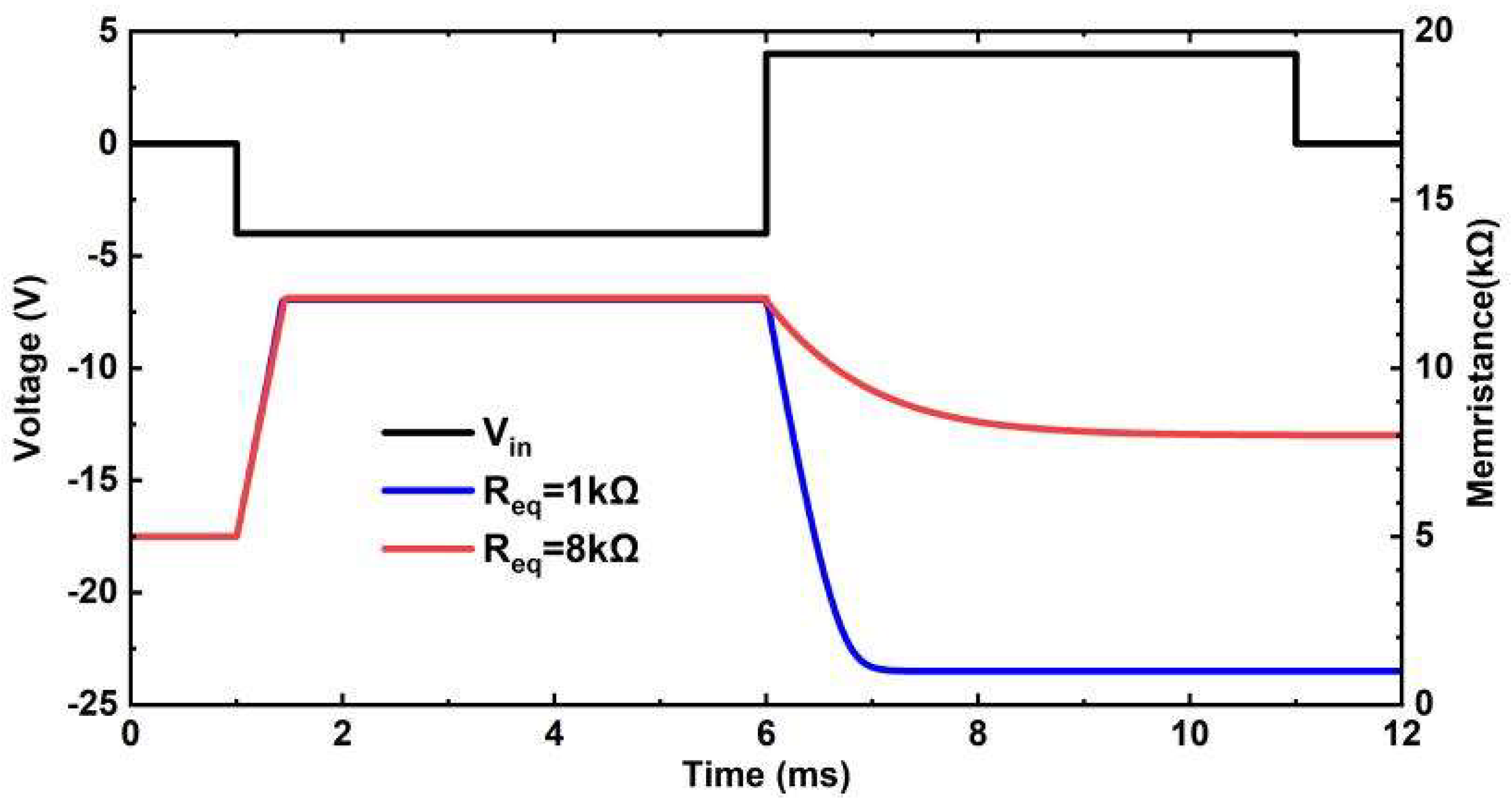
Figure 5. shows the simulation result of the memristor programmable circuit. The width of the programming process is 10ms. The first 0-5ms is the period of Step 1, during which the memristor RESET and the memristance increases to
. And the following 5-10ms is the period of Step 2, during which the memristor SET and the memristance decrease to the aim value. When the reference resistor is
, the memristance simulation result is 0.9999
, compared with reference resistor
R, the accuracy of the simulation result is more than 99%. When the reference resistor is
R, the memristance simulation result is 8.0097
; corresponding to a more than 99% simulation accuracy. The simulation result shows that the programmable circuit function is correct, and the circuit has high precision.
3. Reference Resistor Control Circuit
3.1. The Reference Resistor Circuit
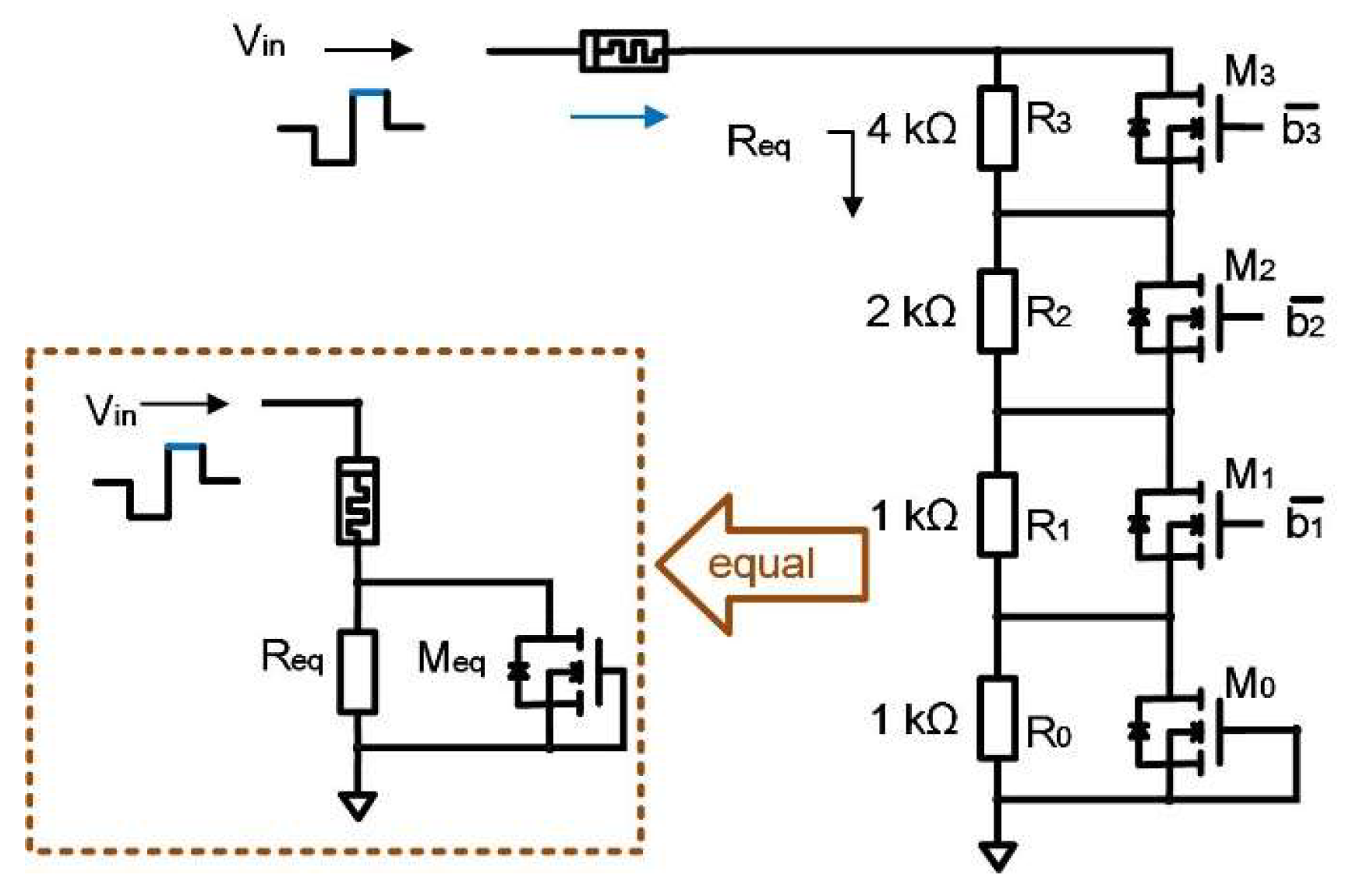
The reference resistor circuit is shown in
Figure 6., which is composed of four NMOSs and four resistors. Different from the same type of NMOSs, the resistors are selected with 1
、1
、2
、4
. The four different resistors can achieve different
values. The control signals are
, which are input digital signals. The reference resistor value is
where
、、、 are reference resistors;
are input digital control signals.
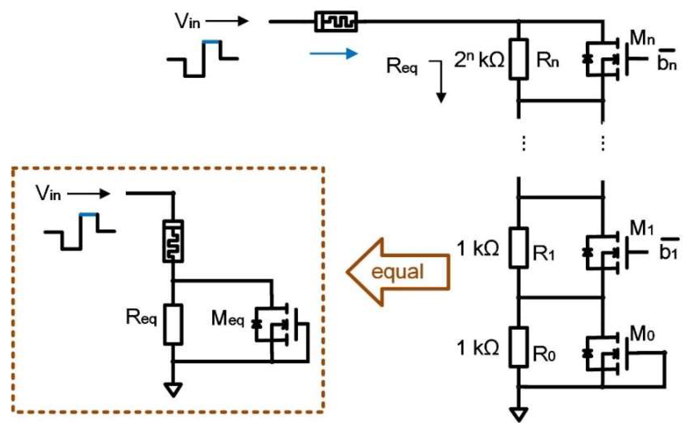
The memristor programming circuit can be adjusted to be controlled by more digital input signals, thus the memristor could be programmed to multi-level states. As is shown in
Figure 7.
are the control digital signals which can program memristor to multi-level memristance. The reference resistor value is
where
、、… 、 are reference resistors;
are digital control signals;
3.2. The Simulation of the Reference Resistor Circuit
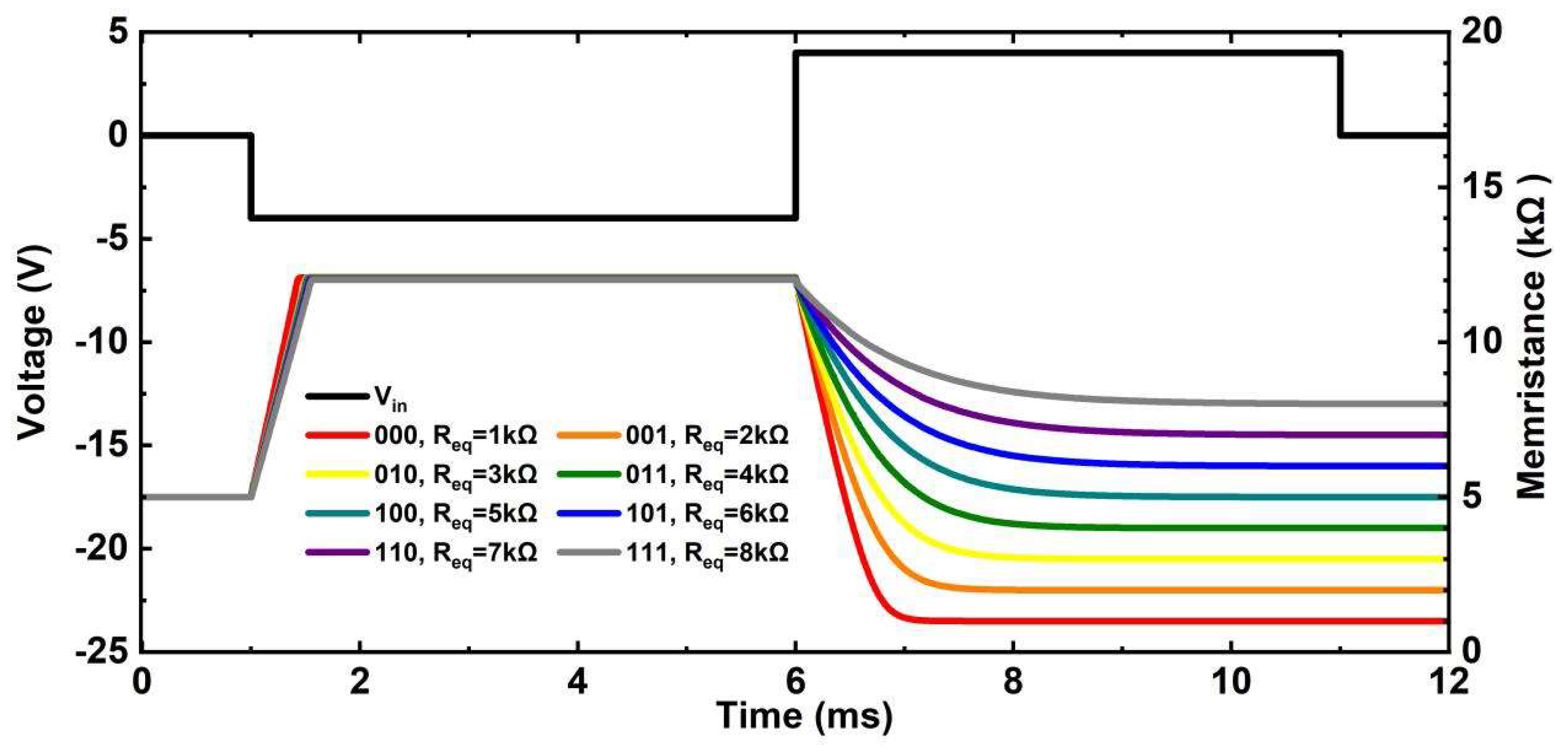
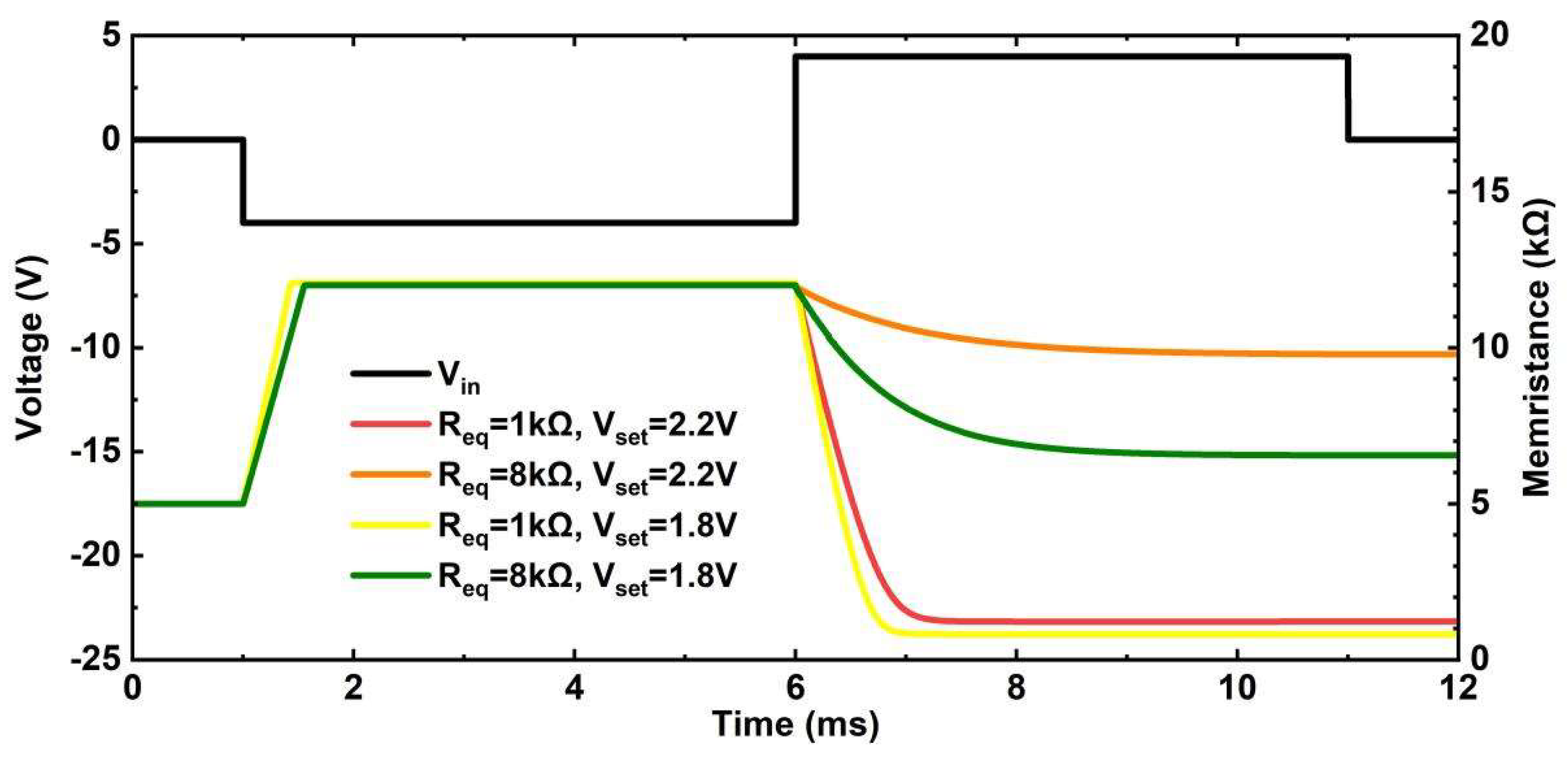
The simulation results are shown in
Figure 8. The programming time cycle is 10ms. The first 5ms is the period of Step 1, and in this period the memristor can be reset to
. And the second 5ms is the period of Step 2, and in this period the memristor will be set to the aim value. When
, the memristance simulation results are 1.0001
、 2.0003
、 3.0001
、 4.0016
、 5.0005
、 6.0023
、 7.0045
、 8.0087
, respectively. All of these simulation results keep 99% programming precision with
.
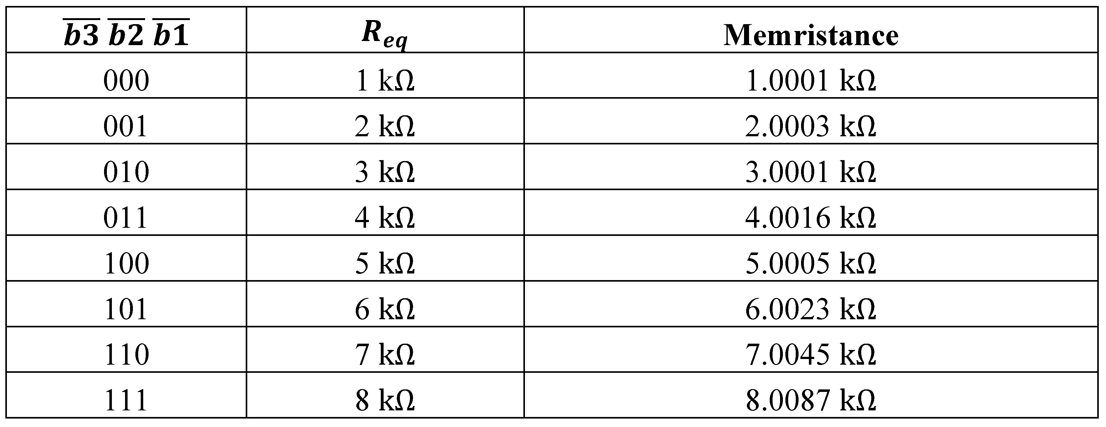
Table 1 shows the relationship between
and
; The digital input signals are
, and the equivalent reference resistor is
, respectively. The memristance simulation results are also shown in
Table 1.
4. Precision Analysis and simulation
From the formula (7), we know that the tolerances of 、 、 have an influence on memristance precision. In this paper, we only discuss the tolerance of which is a parameter of memristor intrinsic characteristics. Considering memristor has 10% tolerance and assuming the ideal value of is , we discuss two conditions:
Condition 1: memristor
has +10% tolerance,
Condition 2: memristor
has -10% tolerance,
corresponding to bule and red lines in
Figure 9., namely,
and
based on
.
4.1. The Impact of Tolerance
For analysis of the impact of , we also consider memristor has 10% tolerance and assume the ideal value of is , and is the aim value. We discuss two conditions:
Condition 1: memristor has +10% tolerance
When
, the memristance value is
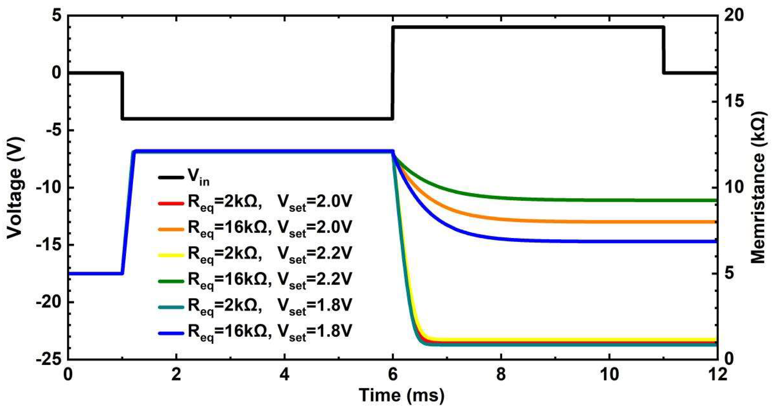
In
Figure 10., when the positive threshold of the memristor is
and the digital input signals are
(
), the simulation value of memristance is
; when the positive threshold of the memristor is
and the digital input signals are
(
), the simulation value of memristance is
. The simulation value of memristance conforms to the theoretical value.
Condition 2: memristor has -10% tolerance
When
, the memristance value is
In
Figure 10., when the positive threshold of the memristor is
and the digital input signals are
(
), the simulation value of memristance is
; when the positive threshold of the memristor is
and the digital input signals are
(
), the simulation value of memristance is
. The simulation value of memristance also conforms to the theoretical value.
5. Optimized Circuit
Through the previous analysis, we know the tolerance of
has an influence on memristance precision. This proposes a solution to optimize the memristance precision by adjusting the values of
and
. However, it does not need to change the structure of the circuit. For example, when
,
,
is the aim value,
is the ideal value), it can still precisely program memristance
. In
Figure 11., when the positive threshold of the memristor is
and the digital input signals are
(
), the simulation value of memristance is
; when the positive threshold of the memristor is
and the digital input signals are
(
), the simulation value of memristance is
. The memristance simulation results are equal to
with an acceptable error. It proves that this solution is effective. Now, considering the tolerance of
, discuss two conditions:
Condition 1: memristor has +10% tolerance
When
In
Figure 11, when the positive threshold of the memristor is
and the digital input signals are
(
), the simulation value of memristance is
; when the digital input signals are
(
), the simulation value of memristance is
; the simulation value of memristance conforms to the theoretical value.
Condition 2: memristor has -10% tolerance
When
In
Figure 11, when the positive threshold of the memristor is
and the digital input signals are
(
), the simulation of memristance is
; when the digital input signals are
(
), the simulation of memristance is
; the simulation value of memristance also conforms to the theoretical value. Condition 1 and condition 2 confirm that properly adjusting the values of
and
can optimize the memristance precision. However, it needs a higher voltage value of source
, so it should make a tradeoff between memristance precision and input voltage value.
6. Memristor Crossbar Programming Circuit
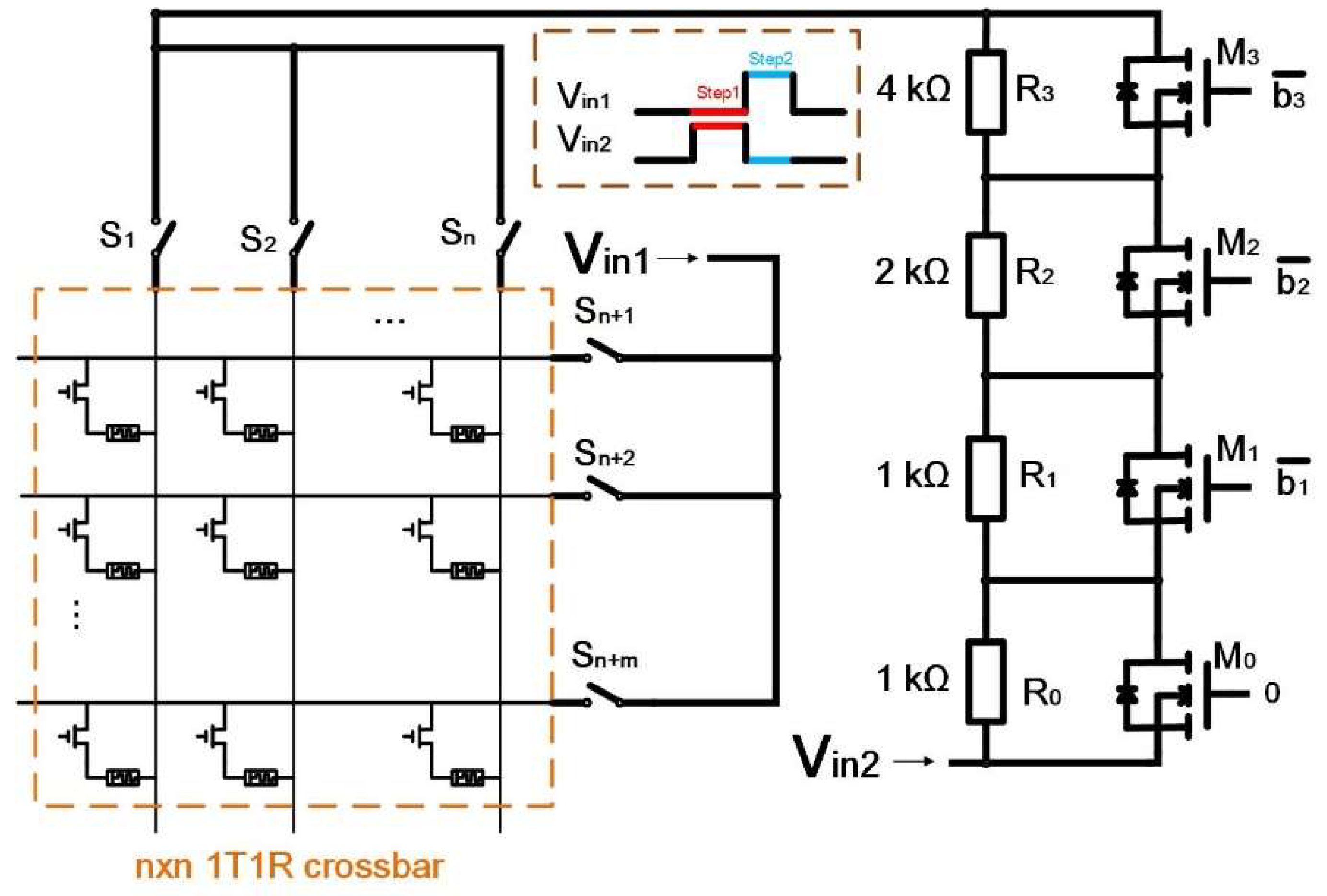
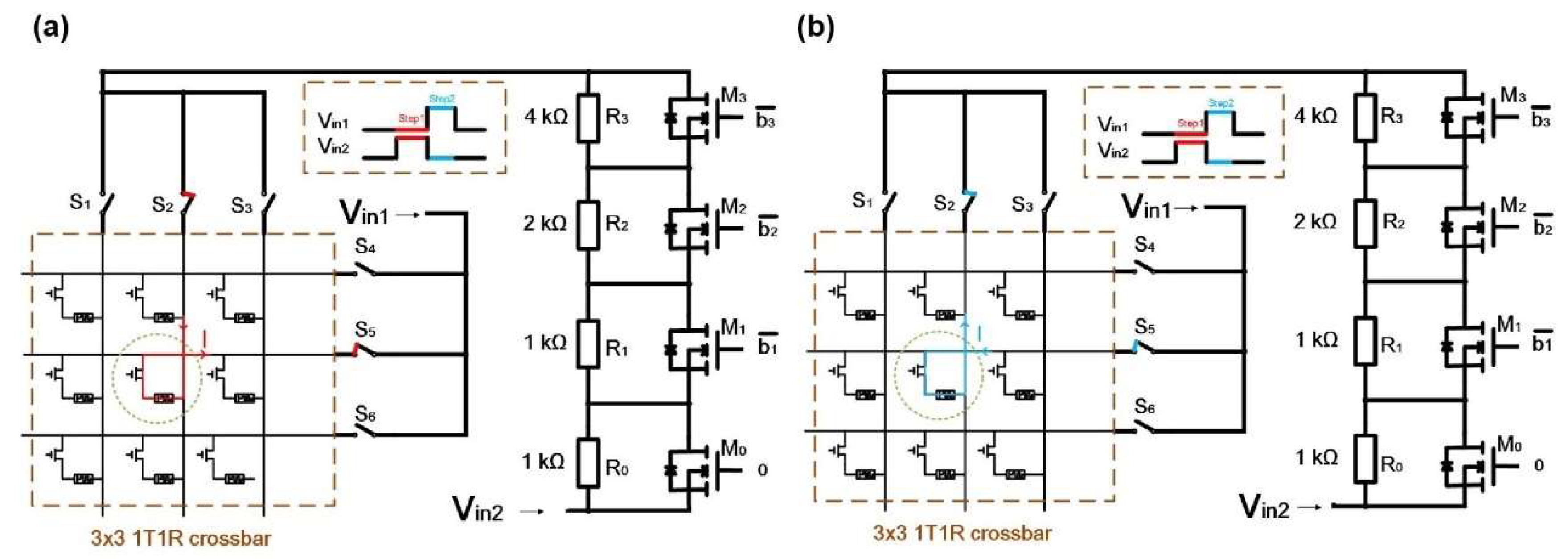
Besides the single memristor device, our programming circuit can also be used to control the memristor crossbar precisely. For example, as shown in
Figure 12., in an mxn 1T1R memristor crossbar, the row signals are controlled by selectors
、、……、, and the column signals are controlled by selectors
、、……、. Through selecting specific row signal and column signal, it can program specific memristor in the memristor crossbar precisely. It also takes two steps to program the memristor. In addition, in the former structure, it uses a single source (
) to program the memristor where a negative pulse is necessary. Here, we use two sources (
) to stimulate the memristor crossbar and these sources are all positive bias.
There are also two steps to program the memristor which is illustrated as follows. Taking an example on a 3x3 1T1R memristor crossbar and the memristor in the second row and second column needs to be updated. In Step1, as in
Figure 13.(a),
is 0V and
is 4V which triggers memristance increases sharply until to
, the memristor completes RESET process. In Step2,
is 4V while the
is 0V which makes the memristance of the memristor is programmed to aim value gradually, and the memristor completes the programming process. The programming process for the other memristors is similar.
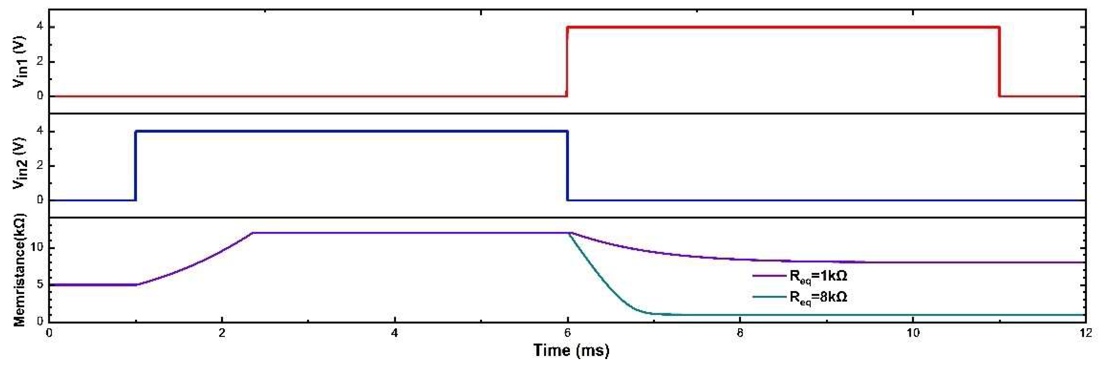
Figure 14 are simulation waveforms, 1-6ms is Step 1, and 6-11ms is Step 2. When the positive threshold of the memristor is
and the digital input signals are
(
), the simulation value of memristance is
; when the digital input signals are
(
), the simulation value of memristance is
. The simulation results agree with the aim values and the precision is more than 99%.
7. Application
With the advent of the big data era, the scale of information has been explosive growth. And the scale of image data is also increasing explosively. However, in the conventional computing architecture, computation and storage is physically separate. It requires frequent data shuttling among the computation and storage units, which causing significant system consumption and speed loss. Hence, it is difficult to emulate the requirements of information analysis and processing [
23,
24,
25]. Memristors with nonvolatility and integrated storage-and-computation properties can be used to build intelligent processing systems that are closer to the structure and function of biological brains [
26,
27]. They are also of great significance for achieving the integrated storage and computation for image data [
28].
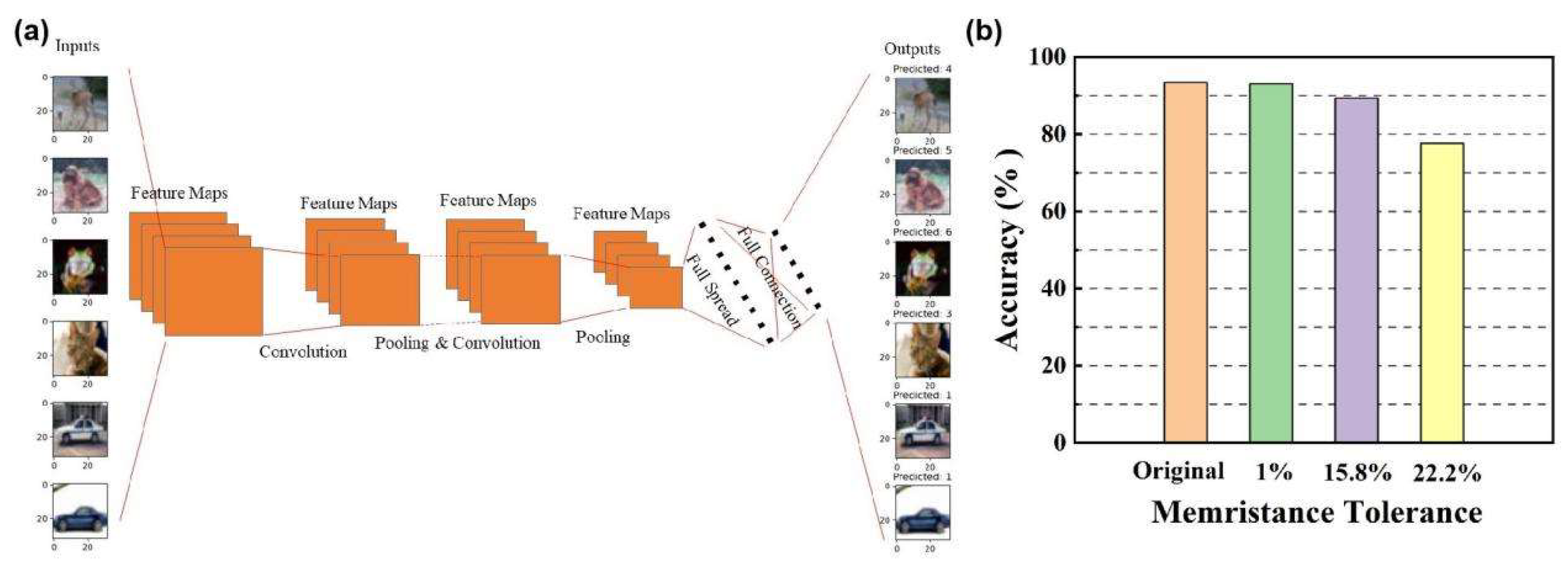
As
Figure 15(a), it is a CNN architecture for image recognition based on memristor crossbar arrays. Inputs are images for recognition, and outputs are the results of recognition. On platform MNSIM [
29], we analyzed the computing accuracy of different memristance tolerance. The algorithm uses VGG8 and the dataset uses CIFAR10. The size of input image is 28x28, hence, the network consists of 784 input neurons. In addition, the numbers of convolution layers and pooling layers are 8 and 5, respectively. And 10 output neurons are corresponding to 10 kinds of classification targets. Hardware configuration is Intel Xeon Gold 6248 @2.50GHz CPU. System is Windows Server 2019 and its word length is 64 bits.
From
Table 2., taking 10% tolerance of
into consideration. As mentioned above, the memristance tolerances of the circuit before and after optimization are 22.22% and 15.8%. Hence, we analyzed the computing accuracy of three memristance tolerance 1%, 15.8%, and 22.2%. As
Figure 7.(b), the computing accuracy is 93.45% (original accuracy). For computing based on memristor crossbar arrays, when the memristance tolerance is 1%, the computing accuracy is 93.09%, and the computing accuracy decreased to 89.36% and 77.64% with the memristance tolerance of 15.8% and 22.22%, respectively. The latency of the network training directly by traditional computer is about 7.47s, while this value decreased to 18.78ms based on memristor crossbar arrays, and the time efficiency improved more than 396 times.
8. Conclusion
In this paper, a novel memristor programming circuit with a reference resistor structure is proposed which can achieve precise memristance, and the function of the circuit has been fully verified by simulation. Just as the memristance adjustment is sensitive to the memristor , this paper analyzed the precision of the memristance under the memristor has ±10% tolerance, and proposed a solution to improve the memristance precision at the cost of increasing input voltage value without changing the circuit structure. In order to complete the circuit design, it should make a tradeoff between the memristance precision and the input voltage value. In addition, this paper demonstrates that the circuit can be applied to the memristor crossbar and the simulation results of the circuit verify the programming function on the memristor crossbar. In the end, this paper analyzed the computing accuracy of different memristance tolerance in the CNN image recognition based on memristor crossbar arrays.
Author Contributions
Direction of the research , Shisheng Xiong; methodology , Shengtao Tu; circuit design, Shengtao Tu; simulation of the circuit, Shengtao Tu; software, Jinyu Li. writing—original draft preparation, Shengtao Tu; writing—review and editing, Shengtao Tu, Shisheng Xiong, Yanyun Ren, and Qin Jiang; All authors have read and agreed to the published version of the manuscript.
Funding
The work was supported by National Natural Science Foundation of China (Nos. U20A20227).
Data Availability Statement
Not applicable.
Conflicts of Interest
The authors declare no conflict of interest.
References
- Chua, L. Memristor-the missing circuit element. IEEE Trans. Circuit Theory 1971, 18, 507–519. [Google Scholar] [CrossRef]
- Strukov, D.B.; Snider, G.S.; Stewart, D.R.; Williams, R.S. The missing memristor found. Nature 2008, 453, 80–83. [Google Scholar] [CrossRef] [PubMed]
- Jiang, Q.; Ren, Y.Y.; Cui, Z.J.; Li, Z.L.; Hu, L.G.; Guo, R.Q.; Duan, S.K.; Xie, S.X.; Zhou, G.D.; Xiong, S.S. CsPbBr3 Perovskite Quantum Dots Embedded in Polystyrene-poly2-vinyl Pyridine Copolymer for Robust and Light-Tunable Memristors. ACS Applied Nano Materials 2023, 6, 8655–8667. [Google Scholar] [CrossRef]
- Yang, X.; Taylor, B.; Wu, A.; Chen, Y.; Chua, L.O. Research progress on memristor: From synapses to computing systems. IEEE Trans. Circuits Syst. I: Regul. Pap. 2022, 69, 1845–1857. [Google Scholar] [CrossRef]
- Ji, X.; Dong, Z.; Lai, C.S.; Qi, D. A brain-inspired in-memory computing system for neuronal communication via memristive circuits. IEEE Commun. Mag. 2022, 60, 100–106. [Google Scholar] [CrossRef]
- Zhong, Y.; Tang, J.; Li, X.; Liang, X.; Liu, Z.; Li, Y.; Xi, Y.; Yao, P.; Hao, Z.; Gao, B.; et al. A memristor-based analogue reservoir computing system for real- time and power-efficient signal processing. Nat. Electron. 2022, 5, 672–681. [Google Scholar] [CrossRef]
- Yoo, J.; Song, H.; Lee, H.; Lim, S.; Kim, S.; Heo, K.; Bae, H. Recent Research for HZO-Based Ferroelectric Memory towards In-Memory Computing Applications. Electronics 2023, 12, 2297. [Google Scholar] [CrossRef]
- Dong, Z.; Ji, X.; Zhou, G.; Gao, M.; Qi, D. Multimodal neuromorphic sensory-processing system with memristor circuits for smart home applications. IEEE Trans. Ind. Appl. 2022. [Google Scholar] [CrossRef]
- Lai, C.S.; Dong, Z.; Qi, D. Memristive Devices and Systems: Modeling, Properties and Applications. Electronics 2023, 12, 765. [Google Scholar] [CrossRef]
- Pershin, Y.V.; Ventra, M.D. Practical Approach to Programmable Analog Circuits with Memristors. IEEE Trans. Circuits Syst. I: Regul. Pap. 2010, 57, 1857–1864. [Google Scholar] [CrossRef]
- Berdan, R.; Prodromakis, T.; Toumazou, C. High Precision Analogue Memristor State Tuning. Electronics Letters 2012, 48, 1105–1107. [Google Scholar] [CrossRef]
- Merced-Grafals, E.J.; Dávila; Noraica; Ge, N.; Williams, R.S.; Strachan, J.P. Repeatable, Accurate, and High Speed Multi-Level Programming of Memristor 1T1R Arrays for Power Efficient Analog Computing Applications. Nanotechnology 2016, 27, 365202. [CrossRef] [PubMed]
- Kim, K.; Yang, J.; Strachan, J. Voltage Divider Effect for the Improvement of Variability and Endurance of TaOx Memristor. Sci Rep 2016, 6, 20085. [Google Scholar] [CrossRef] [PubMed]
- Vourkas, I.; Gómez, J.; Abusleme, Á.; Vasileiadis, N.; Sirakoulis, G.C.; Rubio, A. Exploring the Voltage Divider Approach for Accurate Memristor State Tuning. IEEE 8th Latin American Symposium on Circuits & Systems (LASCAS), Bariloche, Argentina 2017, 1-4.
- Gomez, J.; Vourkas, I.; Abusleme, A.; Sirakoulis, G.C.; Rubio, A. Voltage Divider for Self-Limited Analog State Programing of Memristors. IEEE Transactions on Circuits and Systems II: Express Briefs 2019, 99, 1. [Google Scholar] [CrossRef]
- Olumodeji, O.A.; Gottardi, M. A Pulse-Based Memristor Programming Circuit IEEE International Symposium on Circuits & Systems 2017, 1-4.
- Mokhtar, S.; Wan, F.; Kadiran, K.A.; Rifin, R.; Omar, M. Write and Read Circuit for Memristor Analog Resistance Switching. IEEE 8th Control and System Graduate Research Colloquium (ICSGRC) 2017. [Google Scholar]
- Tarkhan, M.; Maymandi-Nejad, M.; Klidbary, S.H.; Shouraki, S.B. A Bridge Technique for Memristor State Programming. International Journal of Electronics: Theoretical & Experimental 2020, 107, 1015–1030. [Google Scholar]
- Cirera, A.; Fernandez, C.; Vourkas, I.; Rubio, A. Exploring Different Circuit-level Approaches to the Forming of Resistive Random Access Memories. 11th International Conference on Modern Circuits and Systems Technologies (MOCAST), Bremen, Germany 2022, 1-4.
- Lu, W.; Bao, N.; Zheng, T.; Zhang, X.; Song, Y. Memristor-Based Read/Write Circuit with Stable Continuous Read Operation. Electronics 2022, 11, 2018. [Google Scholar] [CrossRef]
- Randrianantenaina, J.L.; Baran, A.Y.; Korkmaz, N. Functional Emulator Designs for a Memristor Model with Programmable Analog and Digital Platforms. Journal of Computational Electronics 2023, 22, 519–530. [Google Scholar] [CrossRef]
- Pershin, Y.V.; Ventra, M.D. SPICE Model of Memristive Devices with Threshold. Radioengineering 2013, 22, 485–489. [Google Scholar]
- Zidan, M.A.; Strachan, J.P.; Lu, W.D. The future of electronics based on memristive systems. Nat. Electron. 2018, 1, 22–29. [Google Scholar] [CrossRef]
- Wang, Z.; Joshi, S.; Savel’ev, S.E.; Jiang, H.; Midya, R.; Lin, P.; Hu, M.; Ge, N.; Strachan, J.P.; Li, Z.; et al. Memristors with diffusive dynamics as synaptic emulators for neuromorphic computing. Nat. Mater. 2017, 16, 101–108. [Google Scholar] [CrossRef] [PubMed]
- Dong, Z.; Sing Lai, C.; Zhang, Z.; Qi, D.; Gao, M.; Duan, S. Neuromorphic extreme learning machines with bimodal memristive synapses. Neurocomputing 2021, 453, 38–49. [Google Scholar] [CrossRef]
- Schuman, C.D.; Potok, T.E.; Patton, R.M.; Birdwell, J.D.; Dean, M.E.; Rose, G.S.; Plank, J.S. A survey of neuromorphic computing and neural networks in hardware. arXiv 2017, arXiv:1705.06963. [Google Scholar]
- Davies, M.; Srinivasa, N.; Lin, T.H.; Chinya, G.; Cao, Y.; Choday, S.H.; Dimou, G.; Joshi, P.; Imam, N.; Jain, S.; et al. Loihi: A neuromorphic manycore processor with on-chip learning. IEEE Micro 2018, 38, 82–99. [Google Scholar] [CrossRef]
- Ji, X.; Dong, Z.; Zhou, G.; Lai, C.S.; Yan, Y.; Qi, D. Memristive System Based Image Processing Technology: A Review and Perspective. Electronics 2021, 10, 3176. [Google Scholar] [CrossRef]
- Xia, L. MNSIM: Simulation Platform for Memristor-Based Neuromorphic Computing System. IEEE Transactions on Computer-Aided Design of Integrated Circuits and Systems 2018, 37, 1009–1022. [Google Scholar]
Figure 1.
Simulation I-V curve of the memristor. is the positive threshold with the value of 2.0V. When the voltage applied to the memristor is greater than 2.0V, the memristance decreases to sharply. is the negative threshold with the value of -2.0V. When the voltage applied to the memristor is less than -2.0V, the memristance increases to sharply.
Figure 2.
Memristor programming circuit. is the memristor that to be programmed, R is the reference resistor and M is the NMOS.
Figure 2.
Memristor programming circuit. is the memristor that to be programmed, R is the reference resistor and M is the NMOS.
Figure 3.
Step 1 of the memristor programming process. In this period, input source is negative. The current flows through M and , as the red arrows in the picture. And the voltage applied to the memristor is negative.
Figure 3.
Step 1 of the memristor programming process. In this period, input source is negative. The current flows through M and , as the red arrows in the picture. And the voltage applied to the memristor is negative.
Figure 4.
Step 2 of the memristor programming process. In this period, input source is positive. The current flows through and R, as the blue arrows in the picture. And the voltage applied to the memristor is positive.
Figure 4.
Step 2 of the memristor programming process. In this period, input source is positive. The current flows through and R, as the blue arrows in the picture. And the voltage applied to the memristor is positive.
Figure 5.
Simulation of the programmable circuit. The black line is the input source , and the value is -4.0V during first 5ms and 4.0V during second 5ms of the pulse. The blue line represents the memristance when the reference resistor is R. The red line represents the memristance when the reference resistor is R.
Figure 6.
The reference resistor circuit with 3-input bits. 、、、 are reference resistors; are digital control signals. The circuit is equivalent to the circuit diagram in the dashed box. is an equivalent resistance. is an equivalent NMOS.
Figure 6.
The reference resistor circuit with 3-input bits. 、、、 are reference resistors; are digital control signals. The circuit is equivalent to the circuit diagram in the dashed box. is an equivalent resistance. is an equivalent NMOS.
Figure 7.
The reference resistor circuit with n-input bits. 、、… 、 are reference resistors; are digital control signals. The circuit is equivalent to a circuit diagram in the dashed box. is the equivalent resistance and is the equivalent NMOS.
Figure 7.
The reference resistor circuit with n-input bits. 、、… 、 are reference resistors; are digital control signals. The circuit is equivalent to a circuit diagram in the dashed box. is the equivalent resistance and is the equivalent NMOS.
Figure 8.
Simulation of the programmable circuit according to different input signals. The black line is the input source . And the color lines are the memristances evolution as the function of different reference resistors.
Figure 8.
Simulation of the programmable circuit according to different input signals. The black line is the input source . And the color lines are the memristances evolution as the function of different reference resistors.
Figure 9.
Simulation I-V curve of the memristor. The red I-V curve is the memristor with the transition voltage of . The blue I-V curve is the memristor with the transition voltage of .
Figure 9.
Simulation I-V curve of the memristor. The red I-V curve is the memristor with the transition voltage of . The blue I-V curve is the memristor with the transition voltage of .
Figure 10.
Simulation precision of the circuit. The black line is the input source , and the color lines are the memristances based on different transition voltage tolerances as the function of stimulation time.
Figure 10.
Simulation precision of the circuit. The black line is the input source , and the color lines are the memristances based on different transition voltage tolerances as the function of stimulation time.
Figure 11.
Simulation of the optimized circuit. The black line is the input source , and the color lines are the memristances evolution based on optimized circuit.
Figure 11.
Simulation of the optimized circuit. The black line is the input source , and the color lines are the memristances evolution based on optimized circuit.
Figure 12.
Memristor crossbar programmable circuit. 、、……、 are the selectors of 1T1R crossbar rows. 、、……、 are the selectors of 1T1R crossbar columns. and are two input sources.
Figure 12.
Memristor crossbar programmable circuit. 、、……、 are the selectors of 1T1R crossbar rows. 、、……、 are the selectors of 1T1R crossbar columns. and are two input sources.
Figure 13.
memristor crossbar programmable circuit. The states of selectors and are ON; while the states of other selectors are OFF. (a) Step1. In this period, input source is 0V and is 4V. (b) Step2. In this period, input source is 0V and is 4V.
Figure 13.
memristor crossbar programmable circuit. The states of selectors and are ON; while the states of other selectors are OFF. (a) Step1. In this period, input source is 0V and is 4V. (b) Step2. In this period, input source is 0V and is 4V.
Figure 14.
Memristor crossbar programmable circuit simulation. The red line is the source , and the value is 0V during 1-6ms and 4.0V during 6-11ms. The blue line is the source , and the value is 4V during 1-6ms and 0V during 6-11ms. The purple line represents the memristance evolution when the reference resistor is and the cyan line represents the memristance evolution when the reference resistor is .
Figure 15.
(a) A CNN architecture for images recognition; (b) Computing accuracy of the different memristance tolerance.
Figure 15.
(a) A CNN architecture for images recognition; (b) Computing accuracy of the different memristance tolerance.
Table 1.
The simulation results based on different and .
Table 1.
The simulation results based on different and .
Table 2.
Memristance precision comparison.
Table 2.
Memristance precision comparison.
Table 3.
Simulation result of memristance.
Table 3.
Simulation result of memristance.
|
Disclaimer/Publisher’s Note: The statements, opinions and data contained in all publications are solely those of the individual author(s) and contributor(s) and not of MDPI and/or the editor(s). MDPI and/or the editor(s) disclaim responsibility for any injury to people or property resulting from any ideas, methods, instructions or products referred to in the content. |
© 2023 by the authors. Licensee MDPI, Basel, Switzerland. This article is an open access article distributed under the terms and conditions of the Creative Commons Attribution (CC BY) license (http://creativecommons.org/licenses/by/4.0/).
