Submitted:
05 June 2023
Posted:
06 June 2023
You are already at the latest version
Abstract
Keywords:
INTRODUCTION
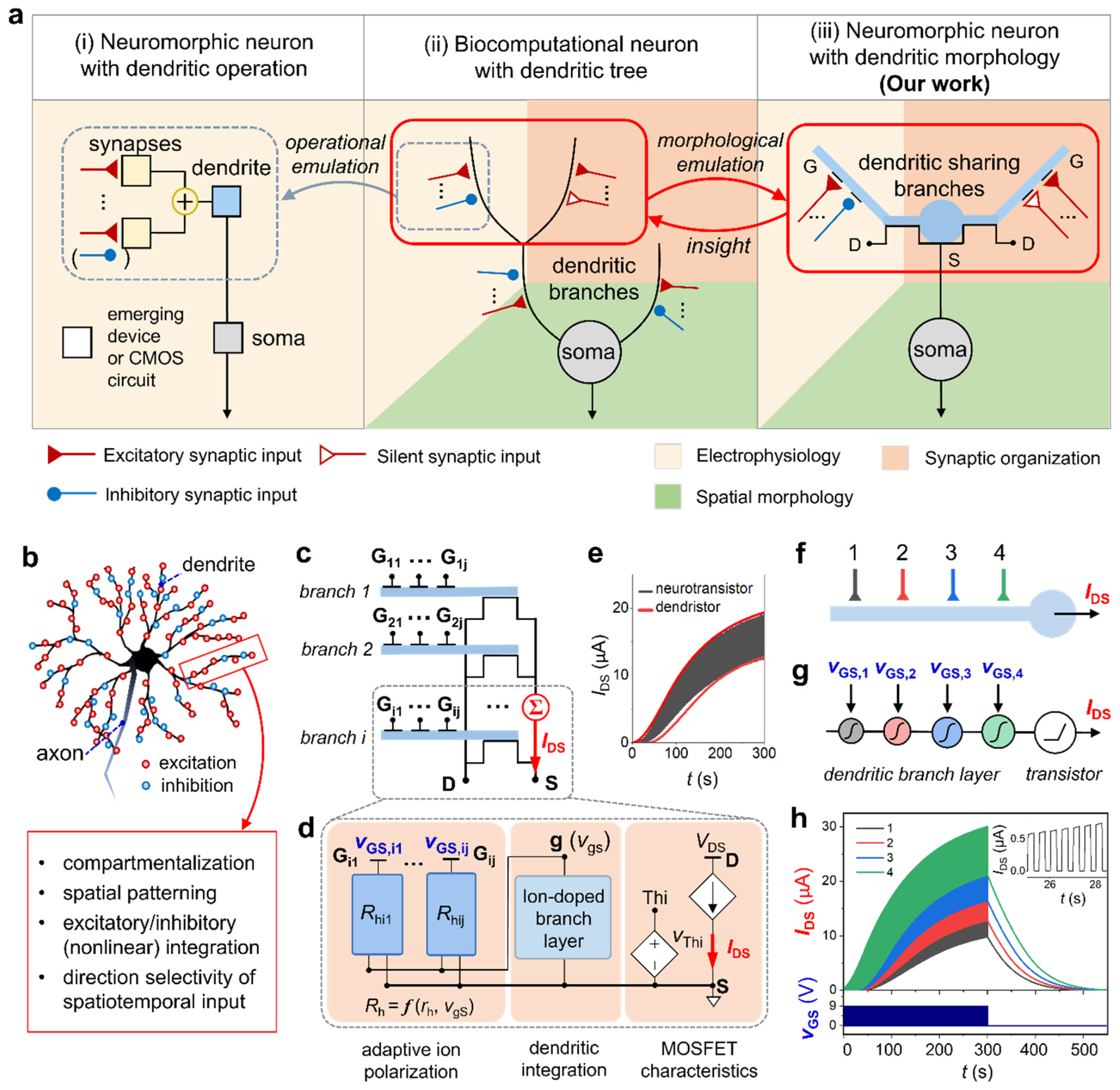
RESULTS
Neuromorphic Dendritic Neuron and Its Output Dynamics
Comparing the Nonlinear Integration of Biological Dendrite and the Dendristor
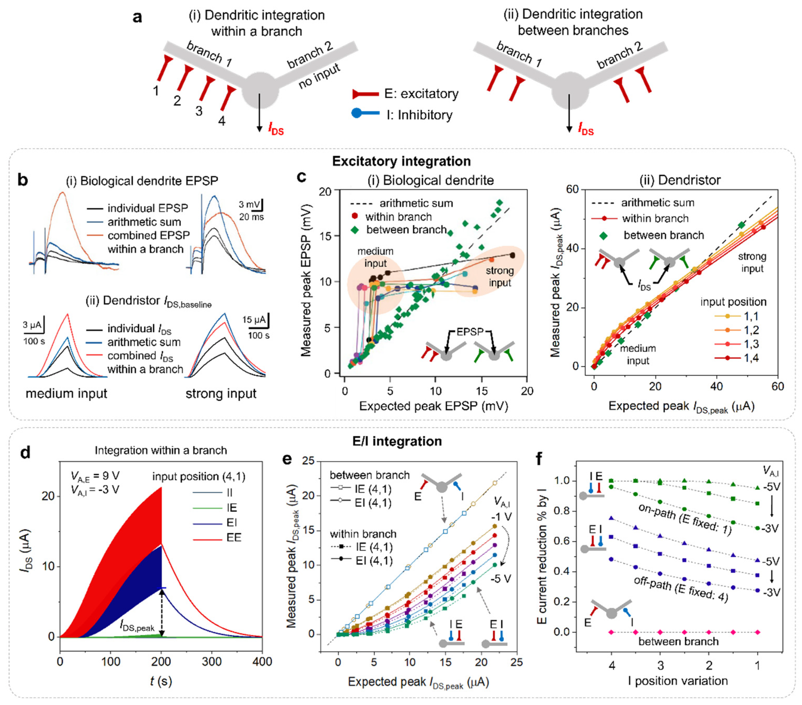
Inhibitory Integration in the Dendristor
Dendritic Direction Selectivity
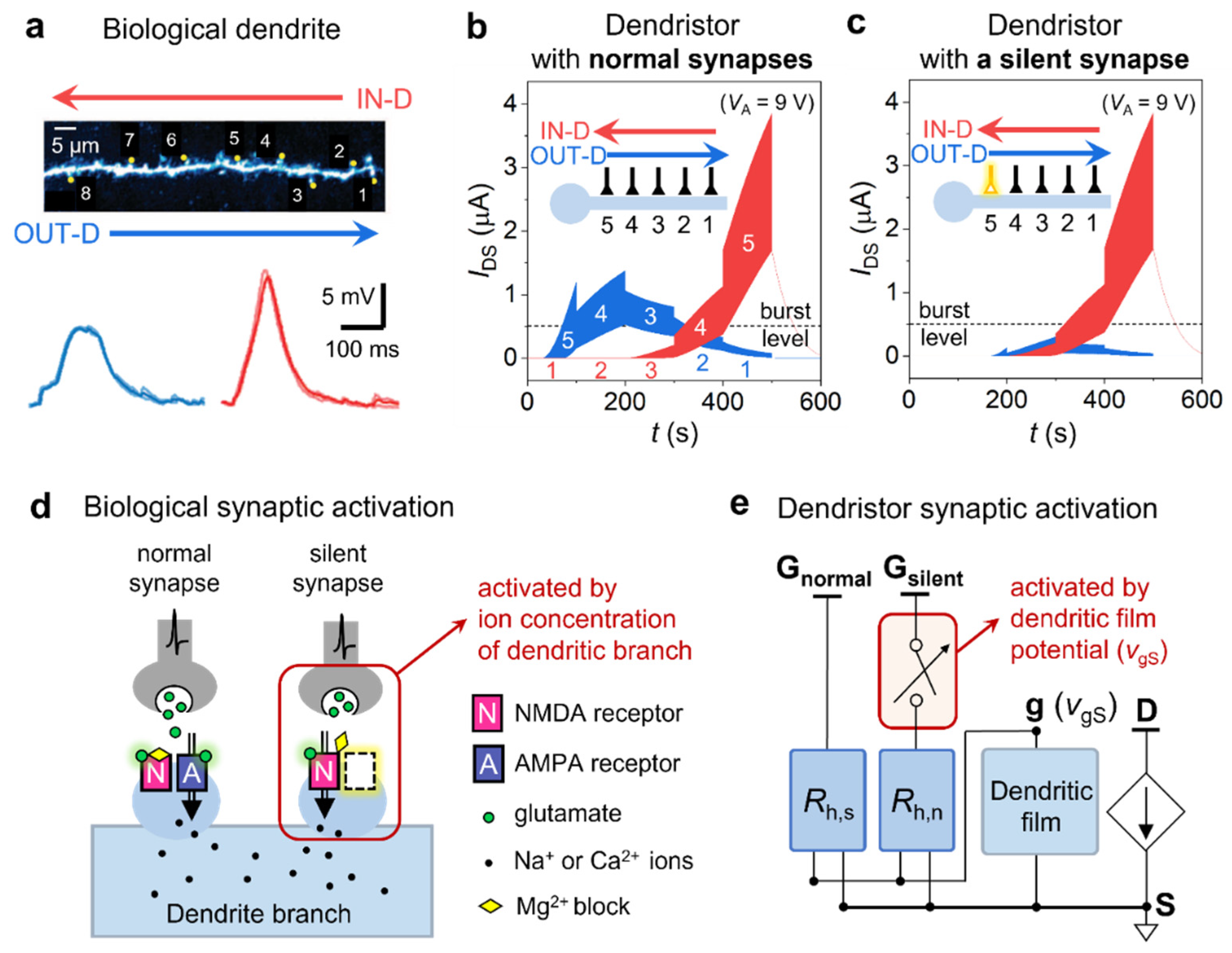
Role of A Silent Synapse in Direction Selectivity
Neuromorphic Dendritic Neural Circuit for Various Motion Detections
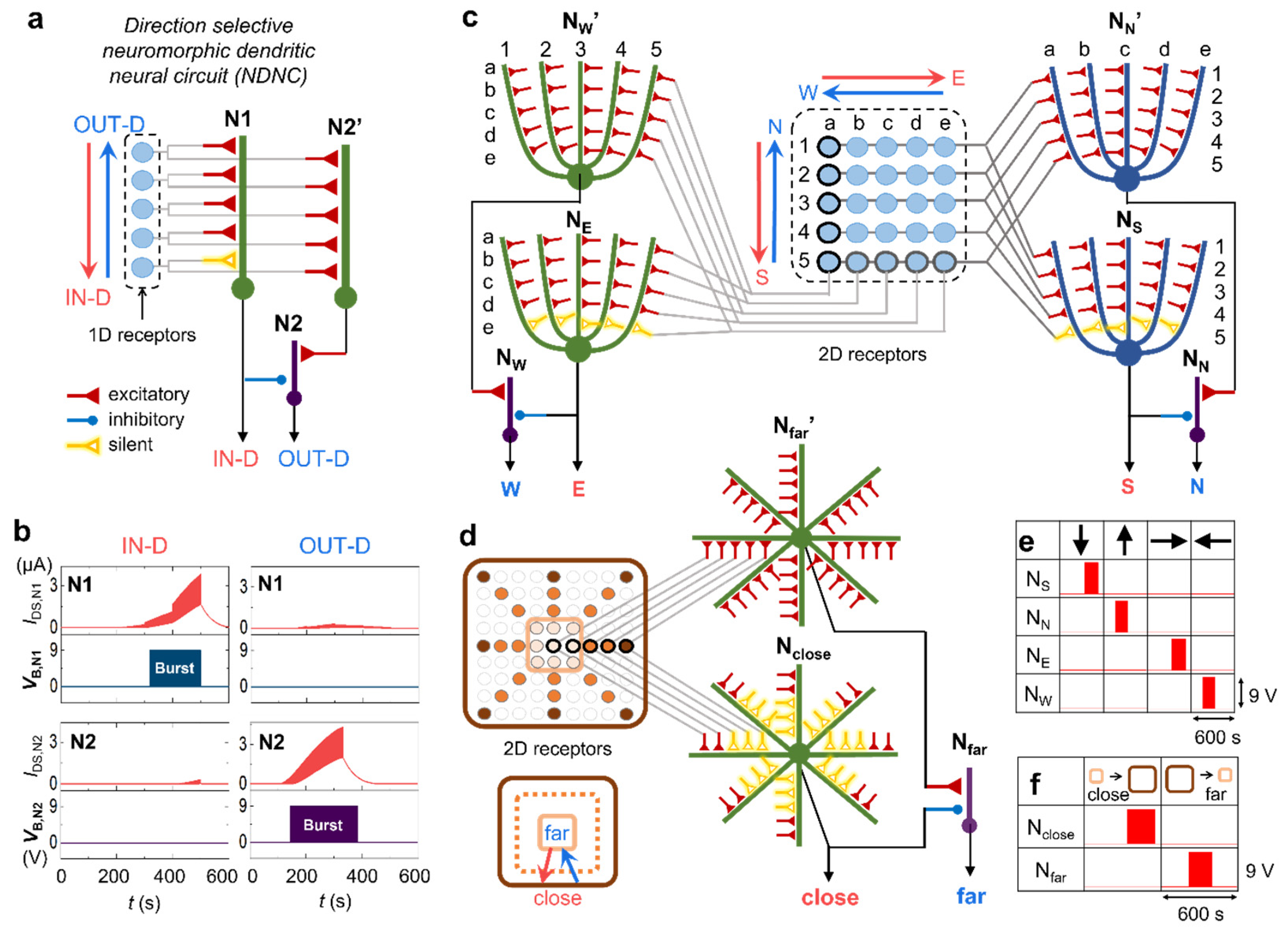
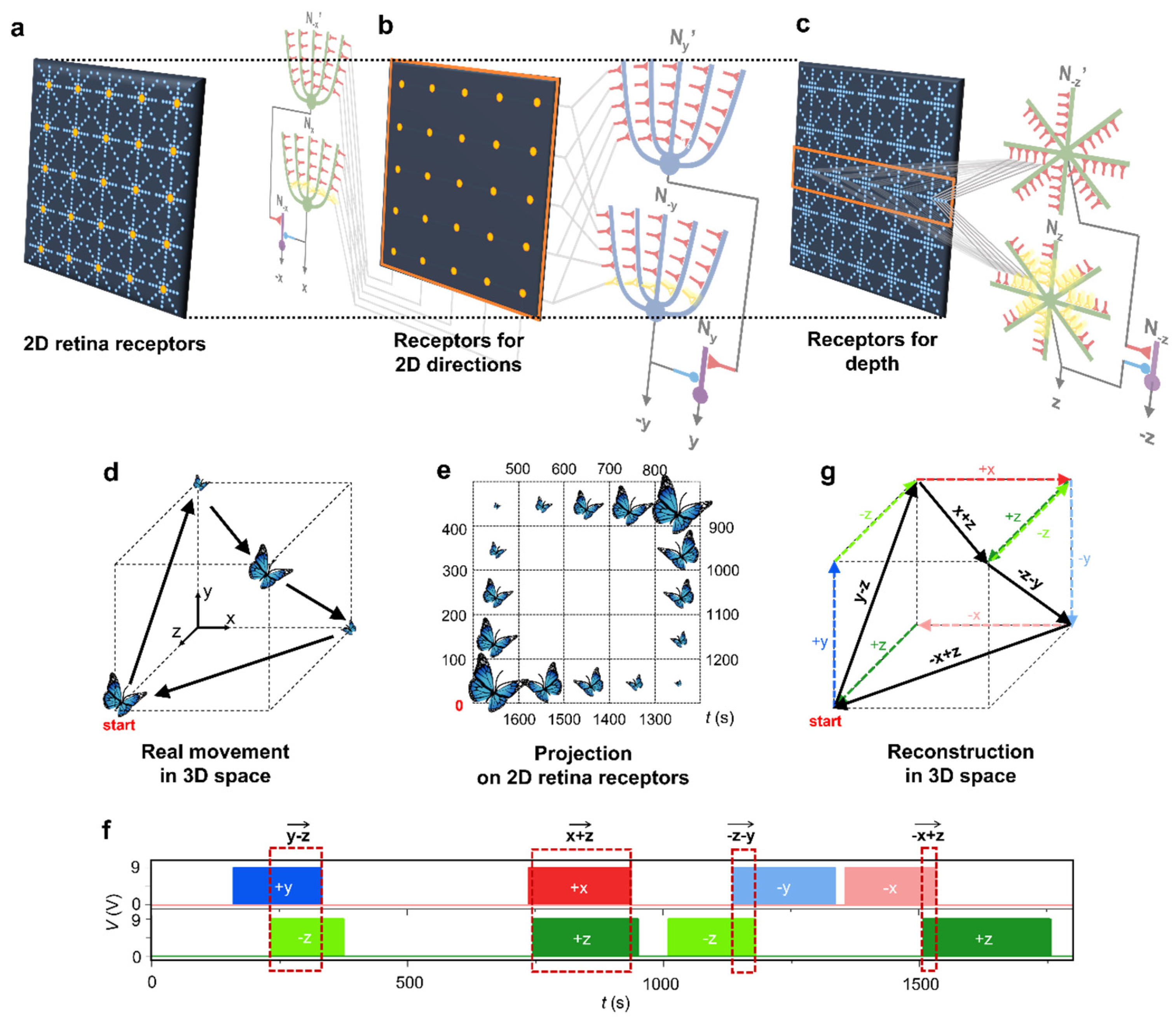
Neuromorphic Visual Perception of Motion in 3D Space
Discussion
Supplementary Materials
Author Contributions
Acknowledgments
Conflicts of Interests
References
- Zhang, W. et al. Neuro-inspired computing chips. Nat Electron 3, 371–382 (2020). [CrossRef]
- Furber, S. B., Galluppi, F., Temple, S. & Plana, L. A. The SpiNNaker project. Proceedings of the IEEE 102, 652–665 (2014). [CrossRef]
- Sen-Bhattacharya, B. et al. Building a Spiking Neural Network Model of the Basal Ganglia on SpiNNaker. IEEE Trans Cogn Dev Syst 10, 823–836 (2018). [CrossRef]
- Casanueva-Morato, D., Ayuso-Martinez, A., Dominguez-Morales, J. P., Jimenez-Fernandez, A. & Jimenez-Moreno, G. Spike-based computational models of bio-inspired memories in the hippocampal CA3 region on SpiNNaker. in 2022 International Joint Conference on Neural Networks (IJCNN) 1–9 (2022). [CrossRef]
- Boybat, I. et al. Neuromorphic computing with multi-memristive synapses. Nat Commun 9, 2514 (2018). [CrossRef]
- Yi, W. et al. Biological plausibility and stochasticity in scalable VO2 active memristor neurons. Nature Communications 2018 9:1 9, 1–10 (2018). [CrossRef]
- Poirazi, P. & Papoutsi, A. Illuminating dendritic function with computational models. Nat Rev Neurosci 21, 303–321 (2020). [CrossRef]
- Ujfalussy, B. B., Makara, J. K., Lengyel, M. & Branco, T. Global and Multiplexed Dendritic Computations under In Vivo-like Conditions. Neuron 100, 579-592.e5 (2018). [CrossRef]
- Sidiropoulou, K., Pissadaki, E. K. & Poirazi, P. Inside the brain of a neuron. EMBO Reports vol. 7 886–892 (2006). [CrossRef]
- Bhalla, U. S. Molecular computation in neurons: A modeling perspective. Current Opinion in Neurobiology vol. 25 31–37 (2014). [CrossRef]
- Marković, D., Mizrahi, A., Querlioz, D. & Grollier, J. Physics for neuromorphic computing. Nature Reviews Physics 2, 499–510 (2020). [CrossRef]
- Zenke, F. et al. Visualizing a joint future of neuroscience and neuromorphic engineering. Neuron 109, 571–575 (2021). [CrossRef]
- Sinz, F. H., Pitkow, X., Reimer, J., Bethge, M. & Tolias, A. S. Engineering a Less Artificial Intelligence. Neuron 103, 967–979 (2019). [CrossRef]
- Cannistraci, C. V., Alanis-Lobato, G. & Ravasi, T. From link-prediction in brain connectomes and protein interactomes to the local-community-paradigm in complex networks. Scientific Reports 2013 3:1 3, 1–14 (2013). [CrossRef]
- Cannistraci, C. V. Modelling Self-Organization in Complex Networks Via a Brain-Inspired Network Automata Theory Improves Link Reliability in Protein Interactomes. Scientific Reports 2018 8:1 8, 1–16 (2018). [CrossRef]
- London, M. & Häusser, M. Dendritic Computation. Annu. Rev. Neurosci 28, 503–535 (2005). [CrossRef]
- Mehonic, A. & Kenyon, A. J. Brain-inspired computing needs a master plan. Nature 604, 255–260 (2022). [CrossRef]
- Boahen, K. Dendrocentric learning for synthetic intelligence. Nature vol. 612 43–50 (2022). [CrossRef]
- Wybo, W. A. M., Torben-Nielsen, B., Nevian, T. & Gewaltig, M. O. Electrical Compartmentalization in Neurons. Cell Rep 26, 1759-1773.e7 (2019). [CrossRef]
- Jarvis, S., Nikolic, K. & Schultz, S. R. Neuronal gain modulability is determined by dendritic morphology: A computational optogenetic study. PLoS Comput Biol 14, 1–21 (2018). [CrossRef]
- Vlasits, A. L. et al. A Role for Synaptic Input Distribution in a Dendritic Computation of Motion Direction in the Retina. Neuron 89, 1317–1330 (2016). [CrossRef]
- Iascone, D. M. et al. Whole-Neuron Synaptic Mapping Reveals Spatially Precise Excitatory/Inhibitory Balance Limiting Dendritic and Somatic Spiking. Neuron 106, 566-578.e8 (2020). [CrossRef]
- Ju, N. et al. Spatiotemporal functional organization of excitatory synaptic inputs onto macaque V1 neurons. Nature Communications 2020 11:1 11, 1–11 (2020). [CrossRef]
- Jones, I. S. & Kording, K. P. Might a single neuron solve interesting machine learning problems through successive computations on its dendritic tree? Neural Comput 33, 1554–1571 (2021). [CrossRef]
- Guerguiev, J., Lillicrap, T. P. & Richards, B. A. Towards deep learning with segregated dendrites. Elife 6, 1–37 (2017). [CrossRef]
- Ujfalussy, B. B., Makara, J. K., Branco, T. & Lengyel, M. Dendritic nonlinearities are tuned for efficient spike-based computations in cortical circuits. Elife 4, 1–51 (2015). [CrossRef]
- Tran-Van-Minh, A. et al. Contribution of sublinear and supralinear dendritic integration to neuronal computations. Front Cell Neurosci 9, 1–15 (2015). [CrossRef]
- Tzilivaki, A., Kastellakis, G. & Poirazi, P. Challenging the point neuron dogma: FS basket cells as 2-stage nonlinear integrators. Nat Commun 10, (2019). [CrossRef]
- Li, S. et al. Dendritic computations captured by an effective point neuron model. Proc Natl Acad Sci U S A 116, 15244–15252 (2019). [CrossRef]
- Goetz, L., Roth, A. & Häusser, M. Active dendrites enable strong but sparse inputs to determine orientation selectivity. Proceedings of the National Academy of Sciences 118, (2021). [CrossRef]
- Takahashi, N., Oertner, T. G., Hegemann, P. & Larkum, M. E. Active cortical dendrites modulate perception. Science (1979) 354, 1587–1590 (2016). [CrossRef]
- Vaney, D. I., Sivyer, B. & Taylor, W. R. Direction selectivity in the retina: Symmetry and asymmetry in structure and function. Nat Rev Neurosci 13, 194–208 (2012). [CrossRef]
- Jia, H., Rochefort, N. L., Chen, X. & Konnerth, A. Dendritic organization of sensory input to cortical neurons in vivo. Nature 464, 1307–1312 (2010). [CrossRef]
- Taylor, W. R., He, S., Levick, W. R. & Vaney, D. I. Dendritic Computation of Direction Selectivity by Retinal Ganglion Cells. Science (1979) 289, 2347–2350 (2000). [CrossRef]
- Mauss, A. S., Vlasits, A., Borst, A. & Feller, M. Visual Circuits for Direction Selectivity. Annu Rev Neurosci 40, 211–230 (2017). [CrossRef]
- Wu, X., Mel, G. C., Strouse, D. J. & Mel, B. W. How dendrites affect online recognition memory. PLoS Computational Biology vol. 15 (2019). [CrossRef]
- Frank, A. C. et al. Hotspots of dendritic spine turnover facilitate clustered spine addition and learning and memory. Nat Commun 9, 1–11 (2018). [CrossRef]
- Kaifosh, P. & Losonczy, A. Mnemonic Functions for Nonlinear Dendritic Integration in Hippocampal Pyramidal Circuits. Neuron 90, 622–634 (2016). [CrossRef]
- Kastellakis, G., Silva, A. J. & Poirazi, P. Linking Memories across Time via Neuronal and Dendritic Overlaps in Model Neurons with Active Dendrites. Cell Rep 17, 1491–1504 (2016). [CrossRef]
- Poirazi, P. & Mel, B. W. Impact of active dendrites and structural plasticity on the memory capacity of neural tissue. Neuron 29, 779–796 (2001). [CrossRef]
- Gidon, A. & Segev, I. Principles Governing the Operation of Synaptic Inhibition in Dendrites. Neuron 75, 330–341 (2012). [CrossRef]
- Malgaroli, A. Silent synapses: I can’t hear you! Could you please speak aloud? Nat Neurosci 2, 3–5 (1999). [CrossRef]
- Kerchner, G. A. & Nicoll, R. A. Silent synapses and the emergence of a postsynaptic mechanism for LTP. Nat Rev Neurosci 9, 813–825 (2008). [CrossRef]
- Vincent-Lamarre, P., Lynn, M. & Béïque, J. C. The Eloquent Silent Synapse. Trends Neurosci 41, 557–559 (2018). [CrossRef]
- Kaiser, J. et al. Emulating Dendritic Computing Paradigms on Analog Neuromorphic Hardware. Neuroscience 489, 290–300 (2022). [CrossRef]
- Cartiglia, M. et al. Stochastic dendrites enable online learning in mixed-signal neuromorphic processing systems. (2022). [CrossRef]
- Li, X. et al. Power-efficient neural network with artificial dendrites. Nat Nanotechnol 15, 776–782 (2020). [CrossRef]
- Baek, E. et al. Intrinsic plasticity of silicon nanowire neurotransistors for dynamic memory and learning functions. Nat Electron 3, 398–408 (2020). [CrossRef]
- Polsky, A., Mel, B. W. & Schiller, J. Computational subunits in thin dendrites of pyramidal cells. Nat Neurosci 7, 621–627 (2004). [CrossRef]
- Vervaeke, K., Lorincz, A., Nusser, Z. & Silver, R. A. Gap junctions compensate for sublinear dendritic integration in an inhibitory network. Science (1979) 335, 1624–1628 (2012). [CrossRef]
- Liu, G. Local structural balance and functional interaction of excitatory and inhibitory synapses in hippocampal dendrites. Nat Neurosci 7, 373–379 (2004). [CrossRef]
- Grienberger, C., Chen, X. & Konnerth, A. Dendritic function in vivo. Trends Neurosci 38, 45–54 (2015). [CrossRef]
- Branco, T., Clark, B. A. & Häusser, M. Dendritic discrimination of temporal input sequences in cortical neurons. Science (1979) 329, 1671–1675 (2010). [CrossRef]
- Hanse, E., Seth, H. & Riebe, I. AMPA-silent synapses in brain development and pathology. Nat Rev Neurosci 14, 839–850 (2013). [CrossRef]
- Xu, W., Löwel, S. & Schlüter, O. M. Silent Synapse-Based Mechanisms of Critical Period Plasticity. Front Cell Neurosci 14, 1–27 (2020). [CrossRef]
- Li, L. et al. Silent synapses generate sparse and orthogonal action potential firing in adult-born hippocampal granule cells. Elife 6, 1–23 (2017). [CrossRef]
- Welchman, A. E. The Human Brain in Depth: How We See in 3D. Annual review of vision science vol. 2 345–376 (2016). [CrossRef]
- Schmidt-Hieber, C. et al. Active dendritic integration as a mechanism for robust and precise grid cell firing. Nat Neurosci 20, 1114–1121 (2017). [CrossRef]
- Lavzin, M., Rapoport, S., Polsky, A., Garion, L. & Schiller, J. Nonlinear dendritic processing determines angular tuning of barrel cortex neurons in vivo. Nature 490, 397–401 (2012). [CrossRef]
- Smith, S. L., Smith, I. T., Branco, T. & Häusser, M. Dendritic spikes enhance stimulus selectivity in cortical neurons in vivo. Nature 503, 115–120 (2013). [CrossRef]
- Whritner, J. A. Visual Perception of Motion in the 3D Environment. (The University of Texas at Austin, 2022). [CrossRef]
- Beniaguev, D., Segev, I. & London, M. Single cortical neurons as deep artificial neural networks. Neuron 109, 2727-2739.e3 (2021). [CrossRef]
- Dominguez-Sanchez, A., Cazorla, M. & Orts-Escolano, S. Pedestrian Movement Direction Recognition Using Convolutional Neural Networks. IEEE Transactions on Intelligent Transportation Systems 18, 3540–3548 (2017). [CrossRef]
Disclaimer/Publisher’s Note: The statements, opinions and data contained in all publications are solely those of the individual author(s) and contributor(s) and not of MDPI and/or the editor(s). MDPI and/or the editor(s) disclaim responsibility for any injury to people or property resulting from any ideas, methods, instructions or products referred to in the content. |
© 2023 by the authors. Licensee MDPI, Basel, Switzerland. This article is an open access article distributed under the terms and conditions of the Creative Commons Attribution (CC BY) license (http://creativecommons.org/licenses/by/4.0/).


