
Submitted:
08 June 2023
Posted:
08 June 2023
You are already at the latest version
Abstract
This paper presents a study aimed at enhancing the performance of quantum dot light-emitting didoes (QLEDs) by employing a solution-processed molybdenum oxide (MoO3) nanoparticle (NP) as a hole injection layer (HIL). The study investigates the impact of varying the concentrations of the MoO3 NP layer on device characteristics and explores the underlying mechanisms responsible for the observed enhancements. Experimental techniques such as an X-ray diffraction and field-emission transmission electron microscopy were employed to confirm the formation of MoO3 NPs during the synthesis process. Ultraviolet photoelectron spectroscopy is employed to analyze the electron structure of the QLEDs. The QLED with an 8 mg/mL concentration of MoO3 nanoparticles achieves remarkable improvements in device performance, with a maximum luminance of 69,240.7 cd/cm2, maximum current efficiency of 56.0 cd/A, and maximum external quantum efficiency (EQE) of 13.2%. The obtained results signify a notable progress in comparison to QLED without HIL and those utilizing the widely used poly(3,4-ethylenedioxythiophene):poly(styrene sulfonate) (PEDOT:PSS) HIL. They exhibit a remarkable enhancement of 59.5% and 26.4% in maximum current efficiency, respectively, as well as a significant improvement of 42.7% and 20.0% in maximum EQE, respectively. This study opens up new possibilities for the selection of HIL and the fabrication of solution-processed QLEDs, contributing to the potential commercialization of these devices in the future.
Keywords:
quantum dot light-emitting diode
; solution process
; MoO3 nanoparticles
; hole injection layer
; charge balance
1. Introduction
Since the groundbreaking report by Colin et al., in 1994 [1], quantum dot (QD) light-emitting diodes (QLEDs) have captured significant attention in the realm of display and solid-state lighting applications. These devices have garnered interest due to their exceptional characteristics, including a narrow spectral emission bandwidth, size-tunable emission wavelength without altering the QD composition, high-efficiency, and a low-cost fabrication technique compatible with solution-processed methods [2,3,4,5,6,7,8,9]. Over the years, rapid technological advancements have propelled the field of QLEDs forward. These advances have primarily stemmed from the development of improved QD materials, inorganic charge transport materials, and more efficient device structures. Furthermore, a deeper understanding of the underlying device physics and manufacturing processes have played a crucial role in enhancing QLED performance and expanding their potential applications. [10,11,12,13,14].
One critical aspect that affects the overall performance of QLEDs is charge injection and transport across the device layers. Efficient and balanced charge injection and transport are essential for achieving high device efficiency, color purity, and operational stability. In traditional QLED structures, the energy barrier for hole injection from the anode to the QD through hole transport layer (HTL) is considerably greater than the energy barrier for electron injection from the cathode to the QD. Consequentially, this leads a charge imbalance of hole and electron carriers within the QD emitting layer (EML). To address this issue, a hole injection layer (HIL) is introduced. The HIL helps to facilitate hole injection into the QD layer, thereby mitigating the charge imbalance and improving overall device performance.
A thin film of poly(3,4-ethylenedioxythiophene):poly(styrene sulfonate) (PEDOT:PSS) is the most widely employed organic HIL in QLEDs owing to its high conductivity, high work function, good thermal stability, high transparency, and electron-blocking ability [15,16,17,18]. However, it is difficult to form a uniform interfacial contact between and PEDOT:PSS and indium tin oxide (ITO) electrode due to the hydrophilicity nature of the PEDOT:PSS [19]. Because the PEDOT:PSS has hygroscopic and acidic properties, it also can lead to the corrosion of ITO electrode, resulting in affecting device performance by degrading device characteristics such as electroluminescence and lifetime [20,21]. In addition, due to the nature of organic materials, the PEDOT:PSS has lower thermal stability than those composed of inorganic materials. Transition metal oxides such as molybdenum oxide (MoO3) [22,23,24], nickel oxide (NiO) [25,26,27], tungsten oxide (WO3) [28,29,30], vanadium oxide (V2O5) [31,32,33] have successfully been employed in QLEDs as promising alternatives to replace the organic PEDOT:PSS HIL due to compatibility with high work function, good stability, and good carrier mobility. In particular, highly n-doped MoO3 has gardened significant attention as a promising material for HIL in QLEDs because it has a deep lying electronic state, efficient hole injection into organic material, and a wide bandgap [34,35,36,37,38]. Furthermore, the solution-processed MoO3 nanoparticles (NPs) exhibits good stability and compatibility with QD synthesis and device fabrication processes.
In this study, we focus on the integration of a solution-processed MoO3 NP HIL in QLED architecture to enhance their performance in terms of efficiency and stability. All layers except for the electrodes were fabricated using a solution-based process. We investigate the influence of varying the MoO3 NP concentration on the device characteristics. Moreover, we explored the underlying mechanisms responsible for the observed improvements in device performance, such as enhanced hole injection, and improved charge balance. The structure and formation of MoO3 NPs during synthesis was confirmed using X-ray diffraction (XRD) and field-emission transmission electron microscopy (FE-TEM). The electronic structure of the QLEDs was analyzed using ultraviolet photoelectron spectroscopy (UPS). The QLED with MoO3 NPs at a concentration of 7 mg/mL achieved a maximum luminance of 69,240.7 cd/cm2, maximum current efficiency of 56.0 cd/A, and maximum external quantum efficiency (EQE) of 13.2%. These values represents a significant advancement compared to QLEDs without HIL and those utilizing the PEDOT:PSS HIL. They demonstrate a remarkable improvement of 59.5% and 26.4% in maximum current efficiency, respectively, and a significant enhancement of 42.7% and 20.0% in maximum external quantum efficiency (EQE), respectively. The findings present new possibilities for selecting hole injection layers and fabricating solution-processed QLEDs, paving the way for their future commercialization.
2. Materials and Methods
2.1. Synthesis of Materials
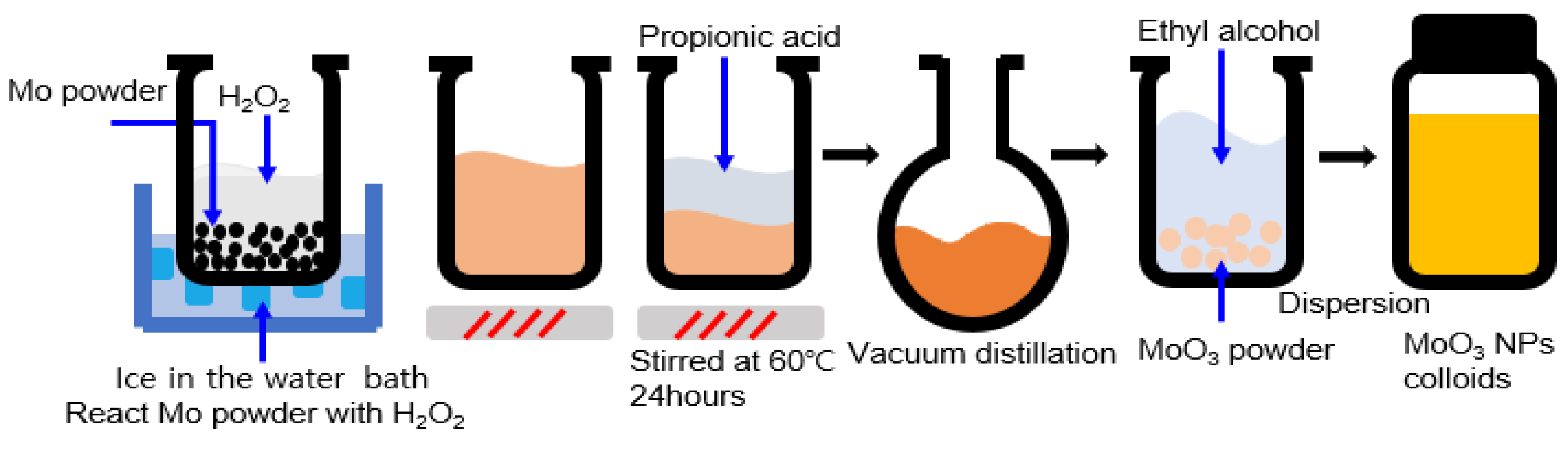
To synthesize MoO3 NPs, 1 g of molybdenum (Mo) powder (Sigma Aldrich) with < 150-nm-size and purity of 99.99% was put in the beaker placed in the ice bath, followed by slowly pouring hydrogen peroxide (H2O2) (Sigma Aldrich) solution of 10 mL in the beaker and stirring for 1h. When the color of the solution was changed from grey to orange, 10 mL of propionic acid (Sigma Aldrich) with purity of 99.5% was added in the solution and stirring at 60ºC for 24 h to ensure that they were fully dissolved. MoO3 powder was obtained after vacuum distillation of the dissolved solution at 50ºC for 30 m. The powder was dispersed in ethanol (EtOH) (Daejung) at pre-determined ratio.
Figure 1.
Schematic illustrating the synthesis process of MoO3 nanoparticles (NPs). .
We synthesized a colloidal suspension of zinc magnesium oxide Zn0.9Mg0.1O NPs by solgel method [39]. To synthesize Zn0.9Mg0.1O NPs, we dissolved 0.2962 g zinc acetate dihydrate Zn(CH3COO)2H2O powder (Sigma Aldrich) and 0.03292 g of magnesium acetate tetrahydrate Mg(CH3COO)4H2O powder (Sigma Aldrich), as precursor materials, in 15 ml of dimethyl sulfoxide (DMSO) (Sigma Aldrich). In a separate step, we dissolved 0.421 g of tetramethyl ammonium (TMAH) (Sigma Aldrich) in 5 ml of EtOH. The TMAH solution was then mixed with the combined solution of Zn(CH3COO)2H2O and Mg(CH3COO)4H2O and stirred at room temperature for 24 h to ensure complete dissolution. To precipitate the Zn0.9Mg0.1O NPs, we added ethyl acetate (Sigma Aldrich) to the synthesized solution in a volume ratio of 3:1. After 3 h, a white powder formed and precipitated. Finally, the Zn0.9Mg0.1O NPs were obtained by centrifuging the solution.
2.2. Device Fabrication
QLEDs were fabricated using following procedure. First, patterned indium tin oxide (ITO) thin films with a sheet resistance of ≤10 Ω/□ served as the anode. Prior to fabrication, the patterned ITO glass substrate underwent a sequential ultrasonic cleaning process using acetone, isopropyl alcohol, methanol, and deionized water. Subsequently, the patterned ITO glass substrate was spin-coated with four layers below:
- A solution of MoO3 NPs was spin-coated onto the ITO substrate at a speed of 2000 rpm for 20 s at room temperature.
- Poly(N-vinyl-carbazole) (PVK) (Sigma Aldrich) was dissolved at a concentration of 1.2 wt%. The PVK solution was then spin-coated onto the patterned ITO glass substrate. The spin-coating process consisted of spinning at 600 rpm for 5 s, followed by spinning at 1500 rpm for 15 s, both at room temperature.
- CdSe/ZnS QDs (Zeus) were dissolved in heptane at a concentration of 5 mg/mL to create the EML. The QD solution was spin-coated onto the ITO/PVK substrate at a speed of 3000 rpm for 5 s at room temperature.
- A solution of Zn0.9Mg0.1O NPs was spin-coated onto the ITO/MoO3/PVK/QD substrate at a speed of 2000 rpm for 20 s at room temperature.
After the spin-coating process, the multilayered substrates were loaded into a high-vacuum deposition chamber (Cetus OL 100; Celcose) with background pressure of 6 × 10⁻⁷ Torr). A 150-nm-thick aluminum (Al) layer was deposited as the cathode using an evaporation rate of 1.2 Å/s. The Al cathode layer was patterned using an in-situ shadow mask to form an active emitting area of 4 mm2.
2.3. Characterizations
The XRD patterns were measured using an X-ray diffractometer (D/Max-2200pc; Rigaku) in the 2θ range of 10º to 60º with a Cu-Kα(λ=1.5405Å) to confirm the formation of MoO3 NPs. FE-TEM images were obtained using a JEOL Tecnai F30 S-Twin microscopy UPS measurements were carried out using an X-ray photoelectron spectroscopy system (K-alpha; Thermo Fisher) equipped with a He (I) 21.22 eV gas discharge lamp to analyze the O1s level and valence band maximum (VBM) of the MoO3 NP thin films. Transmittance and reflectance measurements were performed using a Shimadzu UV-1650PC spectrophotometer with monochromatic light incident on the sample surface. Current density-voltage-luminance (J-V-L) characteristics were evaluated using a computer-controlled source meter (Keithley Instruments) and a luminance meter (LS 100; Konica Minolta). Electroluminescence (EL) spectra were recorded using a Konica Minolta CS1000 spectroradiometer for spectral analysis.
3. Results and Discussion
Figure 2 presents the XRD patterns of the MoO3 NPs obtained by scanning the 2θ range from 10º to 60º. These XRD patterns were analyzed to investigate the crystal structure and crystallite size of MoO3 NPs. The XRD patterns of the MoO3 NPs exhibits an orthorhombic structure, which was confirmed by comparing them to the Joint Committee on Powder Diffraction Standards (JCPDS Card No. 5-0508). A slight shift in the diffraction position and intensity of the MoO3 NPs is observed, suggesting a small distortion in the lattice caused by oxygen vacancies, leading to a change in interatomic spacing. The average crystallite size of the MoO3 NPs was estimated to be 3.60 nm using the Debye-Scherrer equation [40].
Figure 3 displays a FE-TEM image of MoO3 NPs. The average size of the MoO3 NPs was determined to be approximately 3.57 nm, which closely correlates with the result from obtained the XRD analysis.
Figure 4(a) and (b) present the UPS spectra of the valence band edge and secondary electron cutoff regions for various materials including ITO, MoO3 NPs with different concentration, PEDOT:PSS, PVK, QD, and Zn0.9Mg0.1O NPs, aiming to investigate their electronic structures. The spectra were normalized for comparison. The work function (φ) was determined using the equation φ= hν-(Ecutoff -Ecutoff), where hν represents the photon energy (21.22 eV) of the He source and EFermi denotes the Fermi level. The estimated work function for ITO, MoO3 NPs at concentration of 1 mg/ml, 3 mg/ml, 5 mg/ml, 7 mg/ml, 9 mg/ml, PEDOT:PSS, PVK, QD, and Zn0.9Mg0.1O NPs were estimated to be 4.38 eV, 4.69 eV, 4.77 eV, 4.79 eV, 4.88 eV, 4.66 eV, 4.30 eV, 3.98 eV, and 3.54 eV, respectively. The onset energy in the valence band region (Eonset), obtained from the UPS analysis, represents the energy difference between the Fermi level and VBM. Using the work function and Eonset, the VBM values of MoO3 at concentration of 1 mg/ml, 3 mg/ml, 5 mg/ml, and 7 mg/ml were estimated to be 7.79 eV, 7.81 eV, 7.79 eV, and 7.84 eV below the vacuum level, respectively.
In Figure 4(c), (αhν)2 is plotted against the photon energy hν, where α, h, ν represent the absorption coefficient, Planck’s constant, and radiation frequency, respectively. Furthermore, the optical bandgaps of MoO3 NPs at concentration of 1 mg/ml, 3 mg/ml, 5 mg/ml, 7 mg/ml, 9 mg/ml, PEDOT:PSS, PVK, QD, and Zn0.9Mg0.1O NPs were calculated using the optical absorption coefficients obtained from UV-Vis absorption data and the values derived from Tauc equation of (αhν)2=A(hν-Eg) [41], where, A is a constant coefficient and Eg represents the optical bandgap. The calculated optical bandgaps for the MoO3 NPs at concentration of 1 mg/ml, 3 mg/ml, 5 mg/ml, 7 mg/ml, 9 mg/ml, PEDOT:PSS, PVK, QD, and Zn0.9Mg0.1O NPs were determined to be 3.51 eV, 3.50 eV, 3.49 eV, 3.47 eV, 1.92 eV, 3.51 eV, 2.22 eV, and 3.76 eV, respectively, by extrapolating the linear portion of the non-linear curve to the x-axis. Using the optical bandgap estimated from UV-Vis absorption spectra and the VBM values, the conduction band maximum (CBM) levels of the MoO3 NPs at concentration of 1 mg/ml, 3 mg/ml, 5 mg/ml, 7 mg/ml, PEDOT:PSS, PVK, QD, and Zn0.9Mg0.1O NPs were calculated to be 4.28 eV, 4.31 eV, 4.30 eV, 4.37 eV, 3.52 eV, 2.25 eV, 4.95 eV, and 4.02 eV. below the vacuum level, respectively.
Figure 4(d) illustrates the energy level diagram schematic of the QLEDs with the MoO3 NPs at concentration of 1 mg/ml, 3 mg/ml, 5 mg/ml, 7 mg/ml, PEDOT:PSS HILs, PVK HTL, QD EML, Zn0.9Mg0.1O NP ETL in thermal equilibrium. In the energy level diagram, it can be observed that electron injection from Al to the QD layer occurs readily. However, hole injection presents a different scenario due to the deep-lying electronic states of MoO3 NPs. Efficient hole injection is facilitated by electron extraction from the highest occupied molecular orbital (HOMO) level of PVK into the conduction band of MoO3 NPs [42]. In the case of n-doped semiconductors, electron extraction from the HOMO level of the PVK occurs through the MoO3 NP conduction band, followed by injection into ITO.
Figure 5 illustrates the current density and luminance curves as a function of voltage for the QLEDs with varying concentrations of MoO3 NP and PEDOT:PSS HILs. The turn-on voltages extrapolated from the J-V curves for the QLEDs with concentrations of 1 mg/ml, 3 mg/ml, 5 mg/ml, and 7 mg/ml of MoO3 NP, and PEDOT:PSS HILs were determined to be 0.5 V, 1.0 V, 1.5 V, 1.5 V, and 1.5 V, respectively. In contrast, the turn-on voltage for the QLEDs without HILs, such as MoO3 NPs and PEDOT:PSS, was estimated to be 4.0 V. The presence of HILs significantly facilitates hole injection from the ITO to the PVK by reducing the energy barrier between the ITO and PVK. Additionally, from Figure 4, it can be observed that the turn-on voltage is lower when the HIL concentration is as low as 1mg/ml and 3mg/ml. For HIL concentration of 5mg/ml and 7mg/ml, the turn-on voltage remains constant at 1.5 V. We think that the QLEDs with 1-mg/ml, and 3-mg/ml concentrations of MoO3 NP HILs exhibited a small turn-on voltage due to the tunneling phenomenon. On the other hand, we hypothesize that in QLEDs with MoO3 NP HILs at concentrations of 5 mg/ml and 7 mg/ml, electrons from the HOMO level of PVK are extracted to ITO through the MoO3 NP HILs. This process facilitates hole injection by allowing electron extraction from the HOMO level of PVK into ITO through the conduction band of MoO3 NP HILs. At an applied voltage of 16 V, the current densities of the QLEDs with MoO3 NP HILs at concentration of 0 mg/ml, 1 mg/ml, 3 mg/ml, 5 mg/ml, 7 mg/ml, and 9 mg/ml were estimated to be 285.2 mA/cm2, 384.0 mA/cm2, 339.7 mA/cm2, 202.5 mA/cm2, 173.7 mA/cm2, and 0.0 mA/cm2, respectively. As the concentration of MoO3 NPs increased, the thickness also increased, resulting in a decrease in the electric field, which in turn led to a decrease in current density. Among all devices, the QLEDs with PEDOT:PSS HIL exhibited the highest maximum current density. Figure 5 also reveals that no current flowed when a voltage of 16 V was applied to the QLED with a 9 mg/ml concentration of MoO3 NP HIL
The turn-on voltages at 1 cd/m2 for the QLEDs at concentration of 1 mg/ml, 3 mg/ml, 5 mg/ml, 7 mg/ml, and PEDO:PSS were also extrapolated to be 4.68, 4.52, 4.46 V, 4.51 V, and 4.52 V, respectively. The turn-on voltage at 1 cd/m2 for the QLEDs without HILs, such as MoO3 NPs and PEDOT:PSS, was estimated to be 6.58 V. This demonstrates a significant reduction in the turn-on voltage at 1 cd/m2 with the presence of HILs, namely MoO3 NPs and PEDOT:PSS. The QLEDs with 0 mg/ml, 1 mg/ml, 3 mg/ml, 5 mg/ml, 7 mg/ml, and 9 mg/ml concentrations of MoO3 NP HILs achieved maximum luminances of 71,993.7 cd/m2, 109,013.4 cd/m2, 111,781.8 cd/m2, 63,334.8 cd/m2, 69,240.7 cd/m2, and 0.0 cd/m2, respectively. It is observed that with the increase in concentration of MoO3 NP HILs increased from 0 mg/ml to 3 mg/ml, both the current density and maximum luminance increased, leading to a deterioration in the charge balance in QD EML. On the other hand, when the concentration of the MoO3 NP HILs reached 5mg/ml and 7mg/ml, the maximum luminance of the QLEDs decreased. Notably, the QLED with PEDOT:PSS HIL exhibited the highest maximum luminance of 143,510.7 cd/cm2 among all the devices.
Figure 6 illustrates current efficiency and EQE curves as a function of current density for the QLEDs with different concentrations of MoO3 NP and PEDOT:PSS HILs. The maximum current efficiencies of the QLEDs with 0 mg/ml, 1 mg/ml, 3 mg/ml, 5 mg/ml, and 7 mg/ml concentrations of MoO3 NP, and PEDOT:PSS HILs were estimated to be 35.1 cd/A, 45.5 cd/A, 50.4 cd/A, 53.9 cd/A, and 56.0 cd/A, respectively. However, current efficiency of the QLED with a concentration of 10 mg/ml of MoO3 NP HIL did not demonstrate any current flow, thus preventing the measurement of current efficiency. It was observed that as the concentration of the MoO3 NP HILs increased from 0mg/ml to 7mg/ml, the current efficiency improved. These results suggested that thicker MoO3 NP HILs (ranging from 0mg/ml to 7mg/ml) enhance hole injection into the QD EML, achieving better charge balance compared to the relatively high quantity of electrons injected into the QD EML from the Al cathode. In contrast, the QLED with PEDOT:PSS HIL exhibited a maximum current efficiency of 44.3 cd/A. This indicates that while the QLED with PEDOT:PSS HIL achieved higher luminance, it also exhibited higher current density compared to the QLEDs with MoO3 NP HILs, resulting in an inferior charge balance.
Figure 6 also illustrates the maximum EQEs of the QLEDs with MoO3 NP HILs at different concentrations: 0 mg/ml, 1 mg/ml, 3 mg/ml, 5 mg/ml, and 7 mg/ml, which were calculated to be 9.3%, 10.3%, 12.5%, 12.9%, and 13.2%, respectively. As the concentration of the MoO3 NP HILs increased from 0 mg/ml to 7 mg/ml, the EQE also increased, indicating an enhanced charge balance in the QD EML. However, there was a decrease in luminance as the concentration increased from 3mg/ml to 7mg/ml. On the other hand, the QLEDs with PEDOT:PSS HIL exhibited a maximum EQE of 11.0%. Despite its higher luminance, the charge balance of the QLED with PEDOT:PSS is inferior to that of the QLEDs with 3mg/ml, 5mg/ml, 7mg/ml MoO3 NP HILs. Table 1 summarizes the key parameters obtained from the QLEDs with MoO3 NP and PEDOT:PSS HILs.
Figure 7 illustrates the normalized photoluminescence (PL) spectrum of the CdSe/ZnS QD, along with EL spectra from the QLEDs with various concentrations of MoO3 NP and PEDOT:PSS. Table 2 summarizes the characteristics parameters of these spectra, it is noteworthy that the EL peaks of the QLEDs, with both MoO3 NP and PEDOT:PSS HILs, are centered at 532 nm, exhibiting a blue-shift of 12 nm compared to the PL peak of CdSe/ZnS QD. These blue-shifts can be attributed to factors such as Föster energy transfer, dielectric dispersions, and the Stark effect occurring under high voltage and current conditions [43,44,45]. The EL spectra of the QLEDs exhibit no undesired features corresponding to PVK emission, ensuring high color purity. This observation suggests that charge recombination predominantly occurs within the CdSe/ZnS QD EML. Furthermore, Figure 8 demonstrates that the spectra’s full width at half maximum (FWHM) decreases as the concentration of the MoO3 NP HIL increases. Notably, the FWHMs of the spectra for QLEDs with 5 mg/ml and 7 mg/ml MoO3 HILs are narrower compared to the QLED with PEDOT:PSS HIL. The absence of parasitic PVK emission in the narrow confirms that the device emission primarily results from electron-hole recombination within the CdSe/ZnS QD EML. These findings can be attributed to a favorable charge balance between holes and electrons within the CdSe/ZnS QD EML.
4. Conclusions
We investigated the utilization of solution-processed MoO3 NPs as the HIL in QLEDs, aiming to enhance their efficiency and stability. The QLEDs incorporating solution-processed MoO3 NP as the HIL exhibited superior performance compared to those utilizing PEDOT:PSS. The XRD and FE-TEM analyses confirmed that MoO3 NPs with an average size of 3.57 nm were formed through the solution process. Based on the UPS and UV-Vis measurements, the energy level diagram at thermal equilibrium of the QLEDs was constructed. Efficient hole injection is confirmed through the process of electron extraction from the HOMO level of PVK HTL into the conduction band of MoO3 NP HIL, subsequently followed by injection into the ITO anode. The QLED with 8 mg/ml concentration of MoO3 NPs achieved a maximum luminance of 69,240.7 cd/m2, a maximum current efficiency of 56.0 cd/A, and a maximum EQE of 13.2%.
The results represent a significant advancement compared to QLED without HIL and those using the widely used poly(3,4-ethylenedioxythiophene):poly(styrene sulfonate) (PEDOT:PSS) HIL. They demonstrate a remarkable improvement of 59.5% and 26.4% in maximum current efficiency, respectively, as well as a significant enhancement of 42.7% and 20.0% in maximum EQE, respectively. Moreover, the simplicity and low-temperature compatibility of the solution-process preparation method for MoO3 NP thin film, employed in this study, make it suitable for flexible substrate applications. These findings demonstrate the promising potential of MoO3 NPs as the HIL materials, offering a practical and cost-effective platform for the development of large-area QLEDs with exceptional performance and stability.
Author Contributions
H.-H.Y. synthesized materials, fabricated and characterized the devices. G.-P.J., S.-Y.K., Y.-B.C. performed the additional experiments and characterizations. K.-H.Lee performed device characterization. C.K.K. conceptualized this work and wrote the manuscripts. All authors discussed the results and commented on the manuscript. The project was supervised by C.K.K. All authors have read and agreed to the published version of the manuscript.
Funding
This research was partially supported by the Soonchunhyang University Research Fund and also supported by Korea Institute for Advancement of Technology (KIAT) grant funded by the Korea government (MOTIE) (P0012453, The Competency Development Program for Industry Specialist).
Data Availability Statement
The data that supports the findings of this study are available from the corresponding authors upon reasonable request.
Conflicts of Interest
The authors declare no conflict of interest. The funders had no role in the design of the study; in the collection, analyses, or interpretation of data; in the writing of the manuscript, or in the decision to publish the results.
References
- Colin, V.L.; Schlamp, M.C.; Alivisators, A.P., Light-Emitting Diodes Made from Cadmium Selenide Nanocrystals and a Semiconducting Polymers. Nature, 1994, 370, 354–357. [CrossRef]
- Wood, V.; Bulović, V., Colloidal Quantum Dot Light-Emitting Devices, Nano. Rev. 2010, 1, 5202. [CrossRef]
- Lee, S.M. Lee; Shin, D,; Cho, N.-K.; Yi, Y.; Kang, S. J., A Solution-Processable Inorganic Hole Injection Layer that Improves the Performance of Quantum-Dot Light-Emitting Diodes, Curr. Appl. Phys. 2017, 17, 442-447.
- . [CrossRef]
- Bae, W. K.; Lim, J.; Lee, D.; Park, M.; Lee, H.; Kwak, J.; Char, K.: Lee, C.; Lee, S., R/G/B Natural White Light Thin Colloidal Quantum Dot-Based Light-Emitting Devices, Adv. Mater. 2014, 26, 6387-6393. [CrossRef]
- Pan, J.; Chen, J.; Zhao, D.; Huang, Q.; Khan, Q.; Liu, X.; Tao, Z.; Zhang, Z.; Lei, W., Surface Plasmon-enhanced Quantum Dot Light-emitting Diodes by Incorporating Gold Nanoparticles, Opt. Express, 2016, 24, A33–A43.
- . [CrossRef]
- Chang, S.; Zhang, X.; Wang, Z. W.; Han, D. B.; Tang, J. L.; Bai, Z. L.; Zhong, H. Z., Alcohol-Soluble Quantum Dots: Enhanced Solution Processability and Charge Injection for Electroluminescence Devices, IEEE J. Sel. Top. Quantum Electron., 2017, 23, 1900708. [CrossRef]
- Caruge, J. M.; Halpert, J. E.; Wood, V.; Bulovic, V.; Bawendi, M. G., Colloidal Quantum-Dot Light-Emitting Diodes with Metal-Oxide Charge Transport layers, Nature Photonic. 2008, 2, 247-250. [CrossRef]
- Qian, L.; Zheng, Y.; Xue, J.; Holloway, P. H., Stable and Efficient Quantum-Dot Light-Emitting Diodes Based on Solution-Processed Multilayer Structures, Nature Photonics, 2011, 5, 543-548. [CrossRef]
- Shirasaki, Y.; Supran, G. J.; Bawendi, M. G.; Bulović, V., Emergence of Colloidal Quantum-Dot Light-Emitting Technologies, Nature Photon. 2013, 7, 13– 23. [CrossRef]
- Mashford, B. S.; Stevenson, M.; Popovic, Z.; Hamilton, C.; Zhou, Z.; Breen, C.; Steckel, J.; Bulović, V.; Bawendi, M.; Coe-Sullivan, S.; Kazlas, P. T., High-Efficiency Quantum-Dot Light-Emitting Devices with Enhanced Charge Injection, Nat. Photon. 2013, 7, 407-412. [CrossRef]
- Rhee, S.; Kim, K.; Roh, J.; Kwak, J., Recent Progress in High-Luminance Quantum Dot Light-Emitting Diodes, Curr. Opt. Photon. 2020, 4, 161-173. [CrossRef]
- Zhang, Z., Ye, Y.; Pu, C.; Deng, Y.; Dai, X.; Chen, X.; Chen, D.; Zheng, X.; Gao, Y.; Fang, W.; Peng, X.; Jin, Y., High-Performance, Solution-Processed, and Insulating-Layer Free Light-Emitting Diodes Based on Colloidal Quantum dots, Adv. Mater. 2018, 1801387. [CrossRef]
- Li, Y.; Hou, X.; Dai, X.; Yao, Z.; Lv, L.; Jin, Y.; Peng, X., Stoichiometry-Controlled InP-Based Quantum Dots: Synthesis, Photoluminescence, and Electroluminescence, J. Am. Chem. Soc. 2019, 141, 6448-6452. [CrossRef]
- Kwak, J; Bae, W. K.; Lee, D.; Park, I.; Lim, J.; Park, M.; Cho, H.; Woo, H.; Yoon, D. Y.; Char, K.; Lee, S.; Lee, C., Bright and Efficient Full-Color Colloidal Quantum Dot Light-Emitting Diodes Using an Inverted Device Structure, Nano Lett. 2012, 12, 2362-2366. [CrossRef]
- Son, D. I.; Kwon, B. W.; Park, D. H.; Seo, W. S.; Yi, Y.; Angadi, B.; Lee, C. L.; Choi, W. K., Emissive ZnO-Graphene Quantum Dots for White-Light-Emitting Diodes, Nat. Nanotechnol. 2012, 7, 465. [CrossRef]
- Haung, J.; Miller, P. F.; Wilson, J. S.; de Mello, J. C.; Bradly, D. D. C., Investigation of the Effects of Doping and Post-Deposition Treatments on the Conductivity, Morphology, and Work Function of Poly(3,4-ethylenedioxythiophene)/Poly(styrene sulfonate) Films, Adv. Funct. Mater. 2015, 15, 290-296. [CrossRef]
- Murase, S., Yang, Y., Solution Processed MoO3 Interfacial Layer for Organic Photovoltaics Prepared by a Facile Synthesis Method, Adv. Mater. 2012, 24, 2459-2462. [CrossRef]
- Jasieniak, J. J.; Seifter, J.; Jo, J.; Mates, T.; Heeger, J., A Solution-Processed MoOx Anode Interlayer for Use within Organic Photovoltaic Devices, Adv. Func. Mater. 2012, 22, 2594-2605. [CrossRef]
- de Jong, M. P.; van Ijzendoorn, L. J.; de Voigt, M. J. A., Stability of the Interface between Indium-Tin-Oxide and Poly(3,4-Ethylenedioxythiophene)/Poly(Styrenesulfonate) in Polymer Light-Emitting Diodes, Appl. Phys. Lett. 2000, 77, 2255-2257. [CrossRef]
- Yang, X.; Mutlugun, E.; Zhao, Y.; Gao, Y.; Leck, K. S.; Ma, Y.; Ke, L.; Tan, S. T.; Dimir, H. V.; Sun, X. W., Solution Processed Tungsten Oxide Interfacial Layer for Efficient Hole-Injection in Quantum Dot Light-Emitting Diodes, Small, 2014, 10, 247-252. [CrossRef]
- Zheng, Q.; Qu, D.; Zhang, Y.; Li, W.; Xiong, J.; Cai, P.; Xue, X.; Liu, L.; Wang, H.; Zhang, X., Facile Solution-Processed Aqueous MoOx for Feasible Application in Organic Light-Emitting Diode, Opt. Laser Technol. 2018, 101, 85-90. [CrossRef]
- Hwang, J.; Kim, J.; Kim, B.; Park, M.; Kwon, Y.; An, M.; Shin, D.; Jeon, J.; Kim, J.; Lee, W.; Lim, J.; Lee, D., Hole Injection of Quantum Dot Light-Emitting Diodes Facilitated by Multilayered Hole Transport Layer, Appl. Surf. Sci. 2021, 558, 149944. [CrossRef]
- Chen, W.-S.; Yang, S.-H.; Tseng, W.-C.; Chen, W.; Lu, Y.-C., Utilization of Nanoporous Nickel Oxide as the Hole Injection Layer for Quantum Dot Light-Emitting Diodes, ACS Omega, 2021, 6, 13447-13455. [CrossRef]
- Lee, S.; Kim, Y.; Ki, J., Solution-Processed NiO as a Hole Injection Layer for Stable Quantum Dot Light-Emitting Diodes, Appl. Sci. 2021, 11, 4422. [CrossRef]
- Lin, J.; Dai, X.; Liang, X.; Chen, D.; Zheng, X.; Li, Y.; Deng, Y.; Du, H.; Ye, Y.; Chen, D.; Lin, C.; Ma, L.; Bao, Q.; Zhang, H.; Wang, L., High-Performance Quantum-Dot Light-Emitting Diodes Using NiOx Hole-Injection Layers with a High and Stable Work Function, Adv. Funct. Mater. 2020, 30, 1907265. [CrossRef]
- Kim, H.; Lee, D.; Kim, B.; Hwang, B.; Kim, C., Improved Performance of Quantum Dot Light-Emitting Diodes by Introducing WO3 Hole Injection Layers, Mol. Cryst. Liq. Cryst. 2021, 735, 51-60. [CrossRef]
- Chen, L.; Wang, S.; Li, D.; Fang, Y.; H. Shen; L. Li; Z Du, Simultaneous Improvement of Efficiency and Lifetime of Quantum Dot Light-Emitting Diodes with a Bilayer Hole Injection Layer Consisting of PEDOT:PSS and Solution-Processed WO3, ACS Appl. Mater. Interfaces, 2018, 10, 24232. [CrossRef]
- Yao, Y.; Sang, D.; Zou, L.; Wang, Q.; Liu, C., A Review on the Properties and Applications of WO3 Nanostructure-Based Optical and Electronic Devices, Nanomater. 2021, 11, 2136. [CrossRef]
- Choi, S.; Seok, H.; Rhee, S.; Hahm, D.; Bae, W.; Kim, H., Magnetron-Sputtered Amorphous V2O5 Hole Injection Layer for High Performance Quantum Dot Light-Emitting Diode, J. Alloy. Compound. 2021, 878, 160303. [CrossRef]
- Zhang, Y.; Li, W.; Xu, K.; Zheng, Q.; Xu, J.; Zhang, X.; Li, H.; Liu, L., Aqueous Solution-Processed Vanadium Oxide for Efficient Hole Injection Interfacial Layer in Organic Light-Emitting Diode, Phys. Status Solidi A, 2018, 215, 1800047. [CrossRef]
- Heo, S.; Yu, J.; Kim, M.; Yi, Y.; Lee, J.; Kim, H., Interfacial Electronic Structure between a W-doped In2O3 Transparent Electrode and a V2O5 Hole Injection Layer for Inorganic Quantum-Dot Light-Emitting Diodes, RSC Advances, 2019, 9, 11996-12000. [CrossRef]
- Matsushima, T.; Kinoshita, Y.; Murata, H., Formation of Ohmic Hole Injection by Inserting an Ultrathin Layer of Molybdenum Trioxide between Indium Tin Oxide and Organic Hole-Transporting Layers, Appl. Phys. Lett. 2007, 91, 253504. [CrossRef]
- Meyer, J.; Shu, A.; Kröger, M.; Kahn, A., Effect of Contamination on the Electronic Structure and Hole-Injection Properties of MoO3/Organic Semiconductor Interfaces, Appl. Phys. Lett. 2010, 96, 133308. [CrossRef]
- You, H.; Dai, Y.; Zhang, Z.; Ma, D., Improved Performances of Organic Light-Emitting Didoes with Metal Oxide as Anode Buffer, J. Appl. Phys. 2007, 101, 026105. [CrossRef]
- Matsushima, T.; Jin, G.-H.; Murata, H., Marked Improvement in Electroluminescence Characteristics of Organic Light-Emitting Diodes Using an Ultrathin Hole-Injection Layer of Molybdenum Oxide, J. Appl. Phys. 2008, 104, 054501. [CrossRef]
- Zhang, X.; You, F.; Zheng, Q.; Zhang, Z.; Ping, Z.; Cai, P.; Xue, X.; Xiong, J.; Zhang, J., Solution-Processed MoOx Hole Injection Layer Toward Efficient Organic Light-Emitting Diode, Org. Electron. 2016, 39, 43-49. [CrossRef]
- Eun, Y.; Jang, G.; Yang, J.; Kim, S.; Chae, Y.; Ha, M.; Moon, D.; Kim, C., Performance Improvement of Quantum Dot Light-Emitting Diodes Using a ZnMgO Electron Transport Layer with a Core/Shell Structure, Mater. 2023, 16, 600. [CrossRef]
- Alwan, R. M.; Kadhim, Q. A.; Sahan, K. M.; Ali, R., A.; Mahdi, R. J.; Kassim, N. A.; Jassim, A. N., Synthesis of Zinc Oxide Nanoparticles via Sol-Gel Route and Their Characterization, NanoSci. Nanotechnol. 2015, 5(1), 1-6. [CrossRef]
- Viezbicke, B.; Patel, S.; Davis, B.; Birnie, D., Evaluation of the Tauc Method for Optical Absorption Edge Determination: ZnO Thin Films as a Model System, Phys. Status Solidi Basic, 2015, 252, 1700–1710. [CrossRef]
- Lee, S.; Kim, J.; Park, J.; Shin, E.; Roh, Y., Improving Hole Injection Ability Using a Newly Proposed WO3/NiOx Bilayer in Solution Processed Quantum Dot Light-Emitting Diodes, Curr. Appl. Phys. 2022, 38, 81-90. [CrossRef]
- Wood, V.; Panzer, M.; Caruge, J.; Halpert, J.; Bawendi, M.; Bulovic, V., Air-Stable Operation of Transparent, Colloidal Quantum Dot Based LEDs with a Unipolar Device Architecture, Nano Lett. 2010, 10, 24-29. [CrossRef]
- Veijo, J.; Jensen, K.; Mattoussi, H.; Michel, J.; Dabbousi, B.; Bawendi, M., Cathodoluminescence and Photoluminescence of Highly Luminescence CdSe/ZnS Quantum Dot Composite, Appl. Phys. Lett. 1997, 70, 2132-2134. [CrossRef]
- Empedocles, S.; Bawendi, M., Quantum-Confined Stark Effect in Single CdSe Nanocrystallite Quantum Dots, Science, 1997, 278, 2114-2117. [CrossRef]
Figure 2.
X-ray diffraction (XRD) patterns of the MoO3 NPs obtained by scanning the 2θ range from 10º to 60º.
Figure 2.
X-ray diffraction (XRD) patterns of the MoO3 NPs obtained by scanning the 2θ range from 10º to 60º.
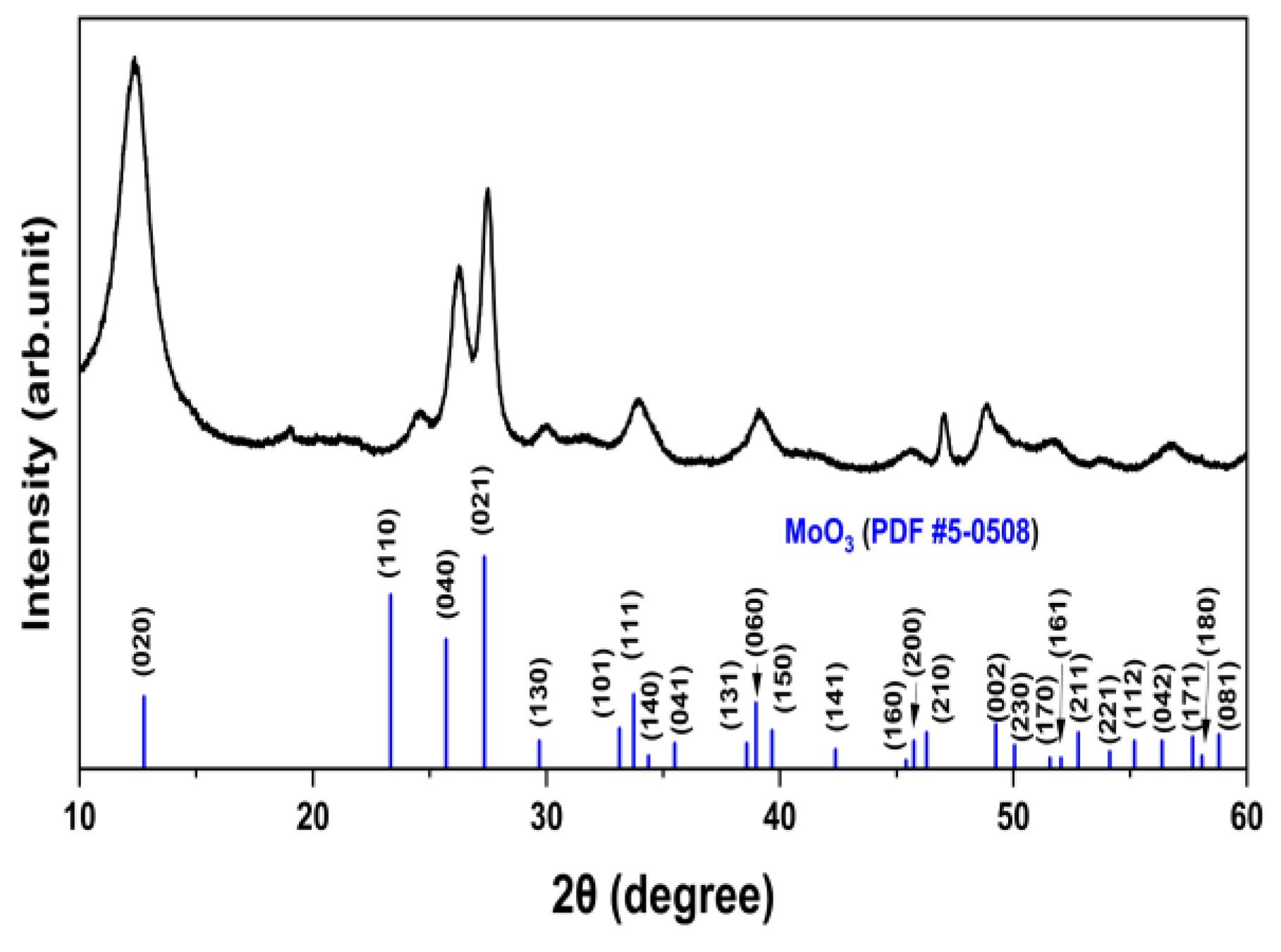
Figure 3.
Field-emission transmission emission microscopy (FE-TEM) image of MoO3 NPs.
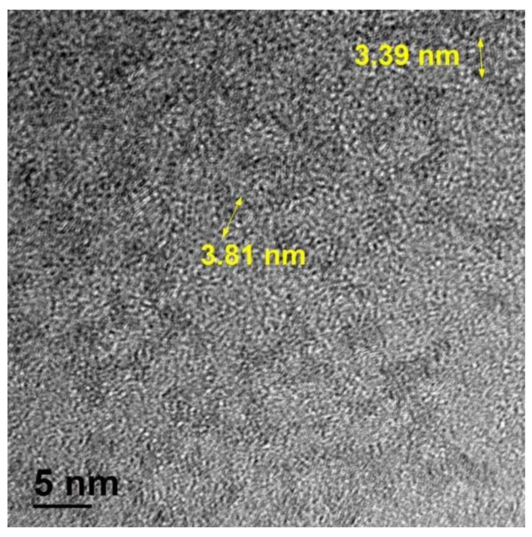
Figure 4.
Ultraviolet photoelectron spectroscopy (UPS) spectra of (a) the valence band edge, (b) secondary electron cutoff regions for various materials including ITO, MoO3 NPs with different concentration, PEDOT:PSS, PVK, QD, and ZnMgO NPs (c). Optical bandgaps of the MoO3 NPs with different concentration, PEDOT:PSS, PVK, QD, and ZnMgO NPs. (d) Schematic energy level diagram of the QLEDs at thermal equilibrium.
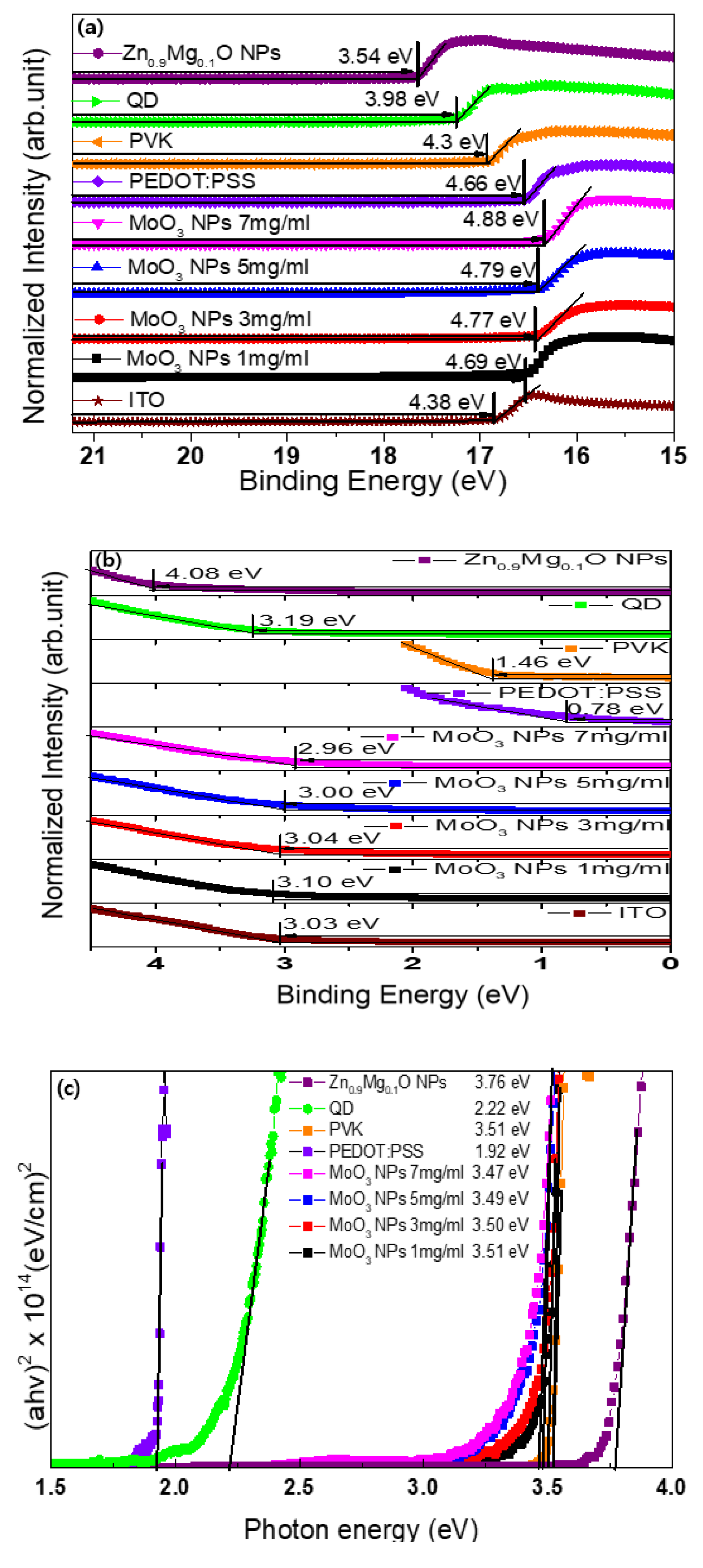
Figure 5.
Current density and luminance curves as a function of voltage for the QLEDs with various concentrations of MoO3 NP and PEDOT:PSS HILs.
Figure 5.
Current density and luminance curves as a function of voltage for the QLEDs with various concentrations of MoO3 NP and PEDOT:PSS HILs.
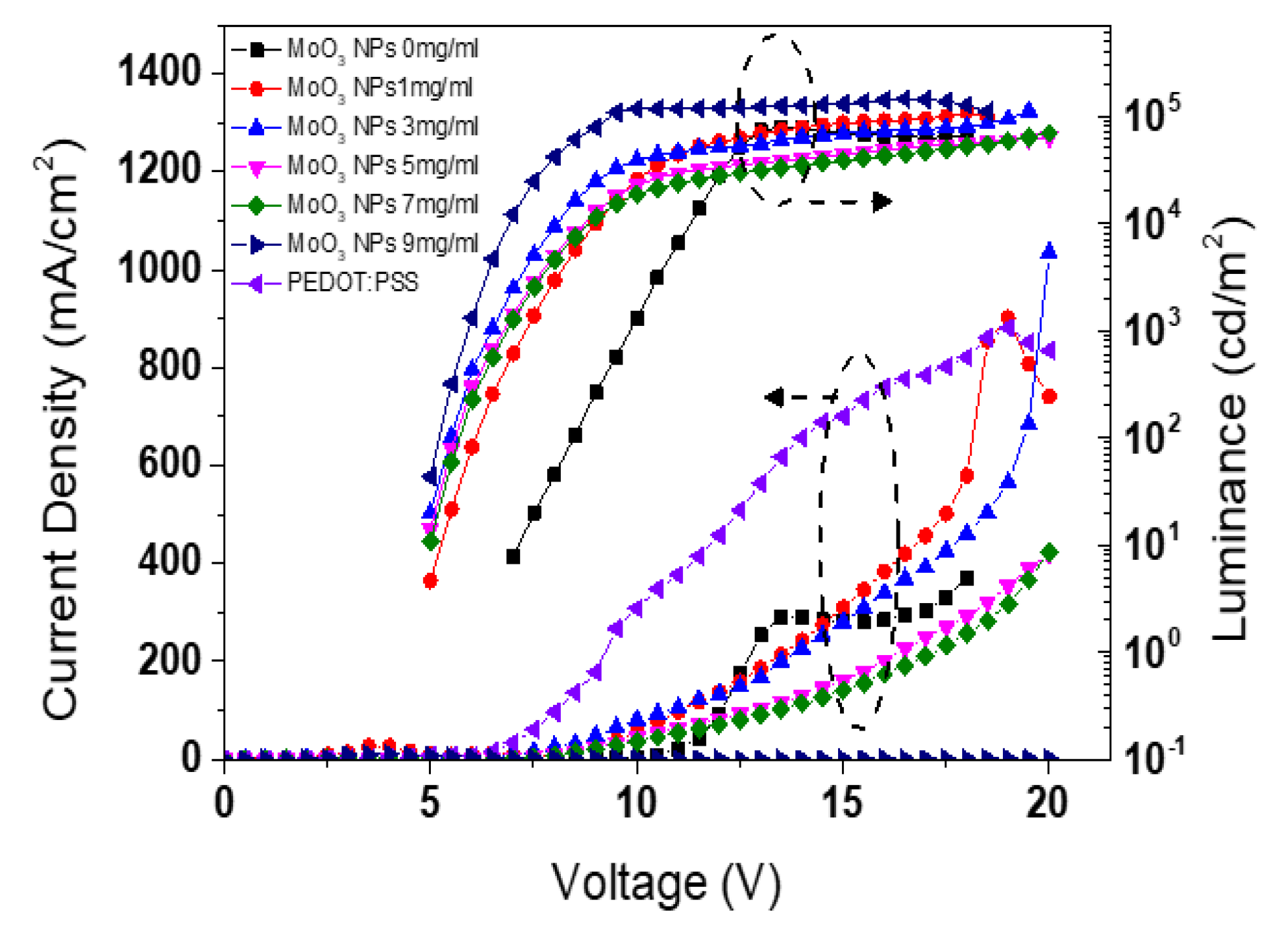
Figure 6.
Current efficiency and EQE curves as a function of current density for the QLEDs with various concentrations of MoO3 NP and PEDOT:PSS HILs.
Figure 6.
Current efficiency and EQE curves as a function of current density for the QLEDs with various concentrations of MoO3 NP and PEDOT:PSS HILs.
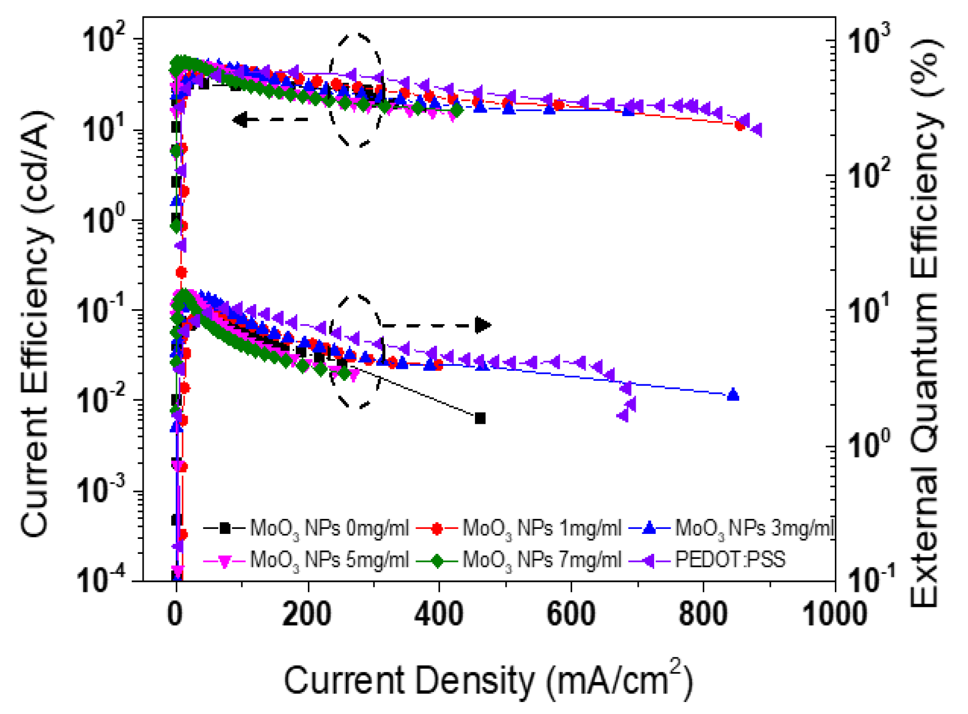
Figure 7.
Normalized photoluminescence (PL) spectrum of the CdSe/ZnS QD and electroluminescence (EL) spectra of the QLEDs with various concentrations of MoO3 NP and PEDOT:PSS.
Figure 7.
Normalized photoluminescence (PL) spectrum of the CdSe/ZnS QD and electroluminescence (EL) spectra of the QLEDs with various concentrations of MoO3 NP and PEDOT:PSS.
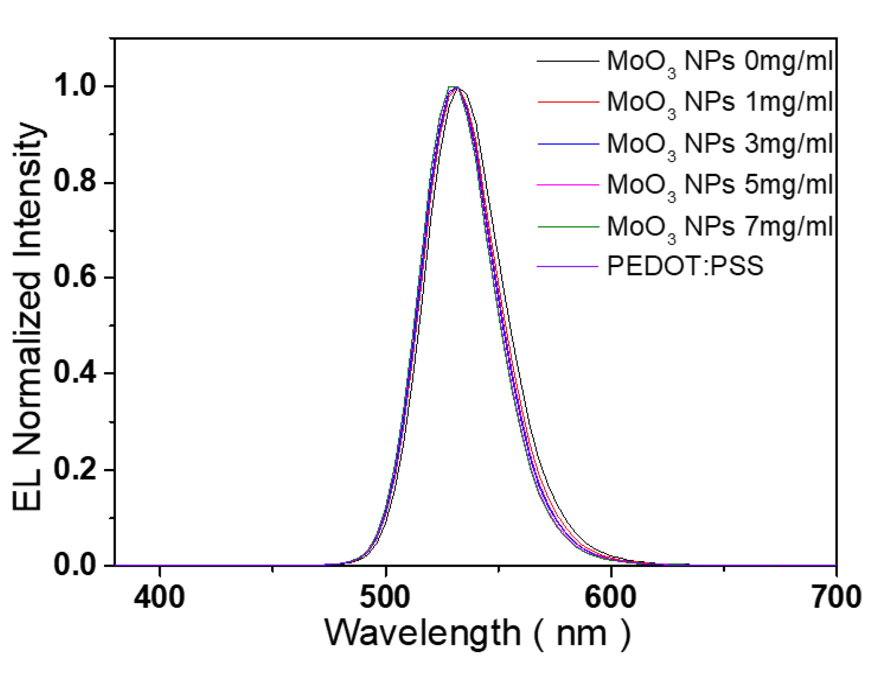

Table 1.
The performance parameters of QLEDs with various concentrations of MoO3 NP, PEDOT:PSS hole injection layers (HILs).
Table 1.
The performance parameters of QLEDs with various concentrations of MoO3 NP, PEDOT:PSS hole injection layers (HILs).
| Types of HIL | Current density at 16 V (mA/cm2) | Maximum luminance (cd/m2) |
Maximum luminous efficiency (cd/A) | Maximum EQE (%) |
| PEDOT:PSS MoO3 NPs of 0 mg/ml |
761.2 285.2 |
143,510.7 71,993.7 |
44.3 35.1 |
11.0 9.25 |
| MoO3 NPs of 1 mg/ml | 384.0 | 109,013.4 | 45.5 | 10.3 |
| MoO3 NPs of 3 mg/ml | 339.7 | 111,781.8 | 50.4 | 12.5 |
| MoO3 NPs of 5 mg/ml | 202.5 | 63,334.8 | 53.9 | 12.9 |
| MoO3 NPs of 7 mg/ml | 173.7 | 69,240.7 | 56.0 | 13.2 |
Table 2.
The key parameters of the spectra, including the photoluminescence of the QD and the electroluminescence of QLEDs with various concentrations of MoO3 NP and PEDOT:PSS HILs.
Table 2.
The key parameters of the spectra, including the photoluminescence of the QD and the electroluminescence of QLEDs with various concentrations of MoO3 NP and PEDOT:PSS HILs.
| sample | Peak (nm) | FWHM (nm) |
| PL of QD | 544 | 33.3 |
| EL of QLED with 0 mg/ml MoO3 NP HIL |
532 | 41.0 |
| EL of QLED with 1 mg/ml MoO3 NP HIL |
532 | 35.9 |
| EL of QLED with 3 mg/ml MoO3 NP HIL |
532 | 36.0 |
| EL of QLED with 5 mg/ml MoO3 NP HIL |
532 | 36.6 |
| EL of QLED with 7 mg/ml MoO3 NP HIL |
532 | 37.2 |
| EL of QLED with PEDOT:PSS HIL | 532 | 39.6 |
Disclaimer/Publisher’s Note: The statements, opinions and data contained in all publications are solely those of the individual author(s) and contributor(s) and not of MDPI and/or the editor(s). MDPI and/or the editor(s) disclaim responsibility for any injury to people or property resulting from any ideas, methods, instructions or products referred to in the content. |
© 2024 by the authors. Licensee MDPI, Basel, Switzerland. This article is an open access article distributed under the terms and conditions of the Creative Commons Attribution (CC BY) license (https://creativecommons.org/licenses/by/4.0/).
Copyright: This open access article is published under a Creative Commons CC BY 4.0 license, which permit the free download, distribution, and reuse, provided that the author and preprint are cited in any reuse.


