Preprint
Article

A Vision of 6th Generation of Fixed Networks (F6G): Challenges and Proposed Directions

Altmetrics

Downloads

331

Views

234

Comments

0

A peer-reviewed article of this preprint also exists.

Submitted:

12 June 2023

Posted:

12 June 2023

You are already at the latest version

Alerts
Abstract
Humankind has entered a new era wherein a main characteristic is the convergence of various technologies providing services exerting major impact upon all aspects of human activity, be it social interactions as well as interactions with the natural environment. Fixed networks are about to play a major role in this convergence, since they form, along with mobile networks, the backbone that provides access to a broad gamut of services, accessible from any point of the globe. It is for this reason that we introduce a forward-looking approach for fixed networks, particularly focused on Fixed 6th Generation (F6G) networks. First, we adopt a novel classification scheme for the main F6G services, comprising six categories. This classification is based on the key service requirements, namely latency, capacity and connectivity. F6G networks differ from those of previous generations (F1G-F5G) in that they concurrently support multiple key requirements. We then propose concrete steps towards transforming the main elements of fixed networks, such as optical transceivers, optical switches etc. such that they satisfy the new F6G service requirements. Our study categorizes the main networking paradigm of optical switching into two categories namely ultra-fast and ultra-high capacity switching, tailored to different service categories. With regard to the transceiver physical layer, we propose: a) use of all-optical processing to mitigate performance barriers of analog to digital and digital to analog converters (ADC/DAC); b) exploitation of optical multi-band transmission, space division-multiplexing and adoption of more efficient modulation formats.
Keywords: 
Subject: Engineering  -   Electrical and Electronic Engineering

1. Introduction

Modern telecommunications are a direct offspring of the second Industrial Revolution, which commenced with the deployment of Public Switched Telephone Network (PSTN) in the second half of 19th century. The third Industrial Revolution led to great advances on electronics and to the introduction of new services, especially the Internet services, exerting profound impact on the way people communicate, work and live. Nowadays, we have entered the fourth Industrial Revolution (I4.0), to lead to convergence of the various processes, like fixed/wireless communication, computing and sensing into a single network entity. The forthcoming transformed network and especially its access part, will concurrently serve as communication medium, sensor and super-computer, providing services to wield major impact all aspects of human activity and the forms of social interaction as well as their interaction with the natural environment [1]. I4.0 marks the dawn of a completely new Epoch where its main characteristic is the convergence and eventually the fusion of those technologies that define our technosphere into a single technological continuum [2,3].
Social interactions are about to deepen through a broad gamut of novel services to be offered to the end-users by the service/network providers and will be emerging in the context of 6th Generation of Fixed networks (F6G). The work of [4] presented the evolution of services as well as the various network layers over the first five fixed network generations (F1G-F5G), based on a layered approach to enable deeper understanding of the key drivers underlying the evolution. In the current work, we focus on F6G services and their requirements, following a dialectical procedure, observing that the limitations of F5G are becoming the novelties of F6G. In particular, we explore the strict requirements demanded of the service/network providers in order to ensure seamless service operation during the entire service life-cycle, such as high bit-rate, low latency, dense connectivity, and more.
Next, we analyze the outstanding challenges and propose stratagems to aid in successfully fulfilling the stringent service requirements, in a cost- and energy-efficient way. In particular, state-of-the-art transceivers are discussed along with novel techniques to scale the bit rate flexibly up to 2 Tb/s. Furthermore, options to enhance the transportation capacity and node connectivity are proposed and elaborated and the interplay between transported capacity and transparent reach is analyzed. Finally, an essential element of optical networks, namely optical switching, is addressed, proposing alternatives to satisfy ultra-high capacity and ultra-low latency demands, while enabling scalability from operating down to a fraction of the spectrum of a channel, up to the full spectral capacity of the entire fiber, whereby channels fully occupy the available bands. The motivation for our work is to highlight the key challenges of F6G networks, and explore solutions to address these challenges at various levels of the network as well as using prior knowledge to make informed predictions up to 2030, about the foreseeable evolution of key metrics, such as attainable per-fiber capacity, data rate per-channel, etc.
This vision article is organized as follows. In Section 2, the key services of the F6G ecosystem along with their requirements are analyzed. Next, in Section 3, all-optical processing is addressed, proposing concrete steps how ‘to get there’, in light of the pros and cons of ADCs and DACs. In Section 4, the barriers to optical transmission are examined, emphasizing how to push F6G capacity even higher, considering methodologies to attain spectrally efficient modulation formats, increased channel counts, and opening up additional transmission degrees-of-freedom by means of space division multiplexing (SDM) via the use of extra fibers, modes or cores. In Section 5, the issue of optical switching is investigated regarding the needs of the F6G ecosystem for both cases of switching, namely ultra-fast vs. ultra-high capacity switching, each one tailored to different performance criteria. Finally, conclusions and references are provided in Section 6.

2. Services and requirements for F6G

2.1. Classification of services

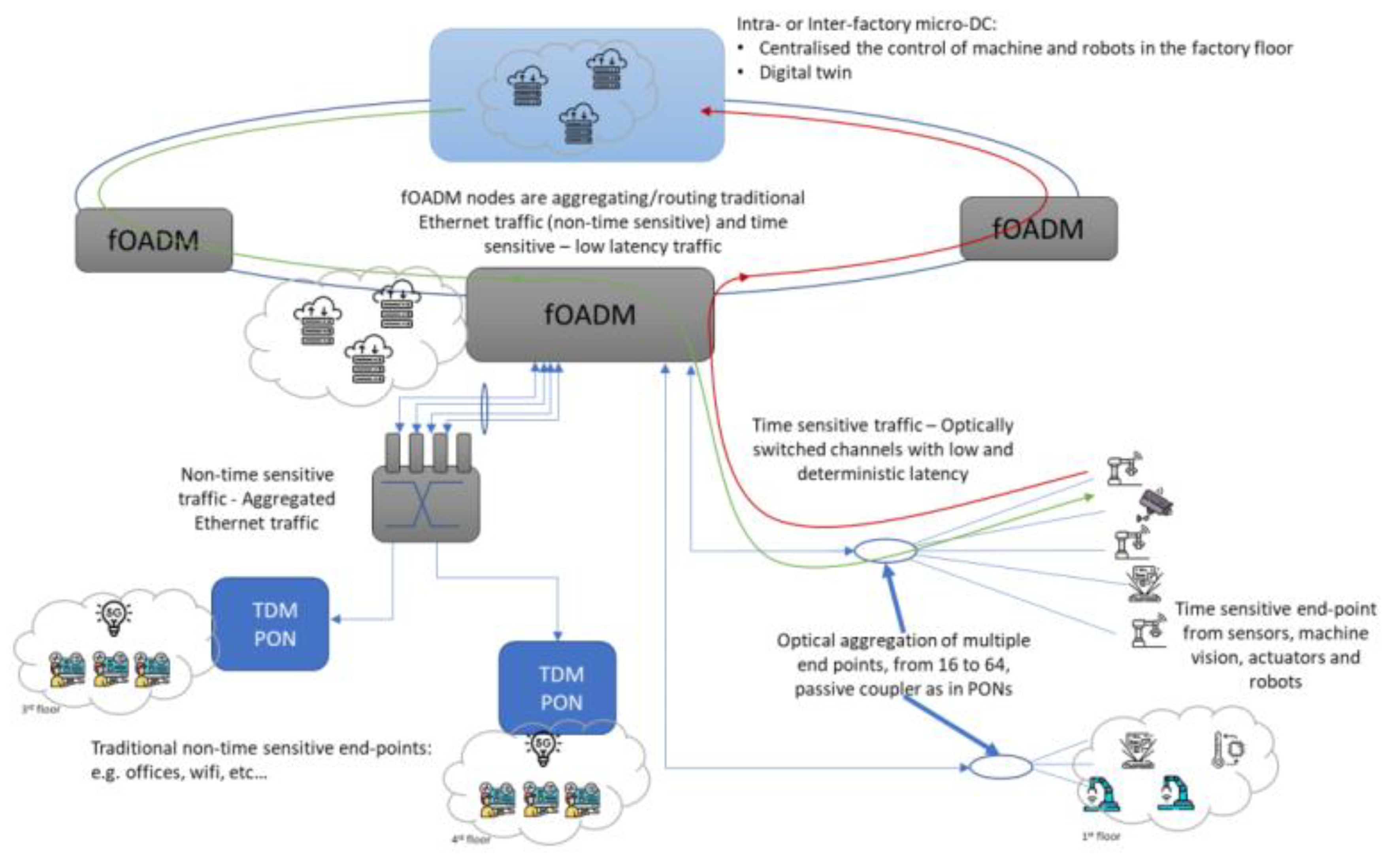
According to F5G group timeline [5,6], today we have entered the 5th generation of fixed networks (F5G) which paves the way for various fresh services, such as augmented and virtual reality, smart city, ultra-high definition (UHD) video streaming, etc. and discussions about the 6th generation (F6G) already take place. The F6G is expected to transform majorly the overall network ecosystem in various dimensions, in order to underpin the stringent requirements of the forthcoming F6G services. Key components for F6G are expected to be a) the industrial sector, e.g. through digital representation of the physical world (digital twin), b) the field of entertainment/communications, e.g. through holograms, internet of senses and mixed reality and c) the transportation sector, mainly through the use of ultra-smart infrastructures, such as airports, ports, highways, cities and railways. To further understand the evolution of services, we illustrate the three key services for each of the six generations of fixed networks in Figure 1.
A main difference of F6G services compared with F5G ones, which poses major challenges in network providers, is that they need to satisfy various strict requirements concurrently in order to ensure a seamless service operation during the entire service life cycle. For example, industrial services such as digital twins require high densification, high bit rate, low latency and high reliability at the same time. In order to ensure this, a significant amount of research work needs to be performed and the network needs to be transformed accordingly, in order to attain (based on the service) increased capacity, lower latency, higher reliability, greater availability, higher densification, lower jitter, etc. and all these using a low cost and low power consumption platform. These requirements can be satisfied through many options, each with its own merits; some indicatives are: new optical wavelength bands, space division multiplexing, high-capacity and ultra-low latency optical switching, free space optical communications, new integration schemes and the use of all-optical processing techniques in Tx/Rx as well as the integration of Artificial Intelligence (AI) / Machine Learning (ML) with the overall network ecosystem. These options and their feasibility along with their advantages are discussed in the current work.
In the next sub-sections of this chapter, we elaborate on the F6G services and their requirements, then we present our vision on the F6G ecosystem and finally we analyze the network transformation which needs to be realized in order to support all the new types of services with their requirements.

2.2. Upcoming categories of services and their requirements

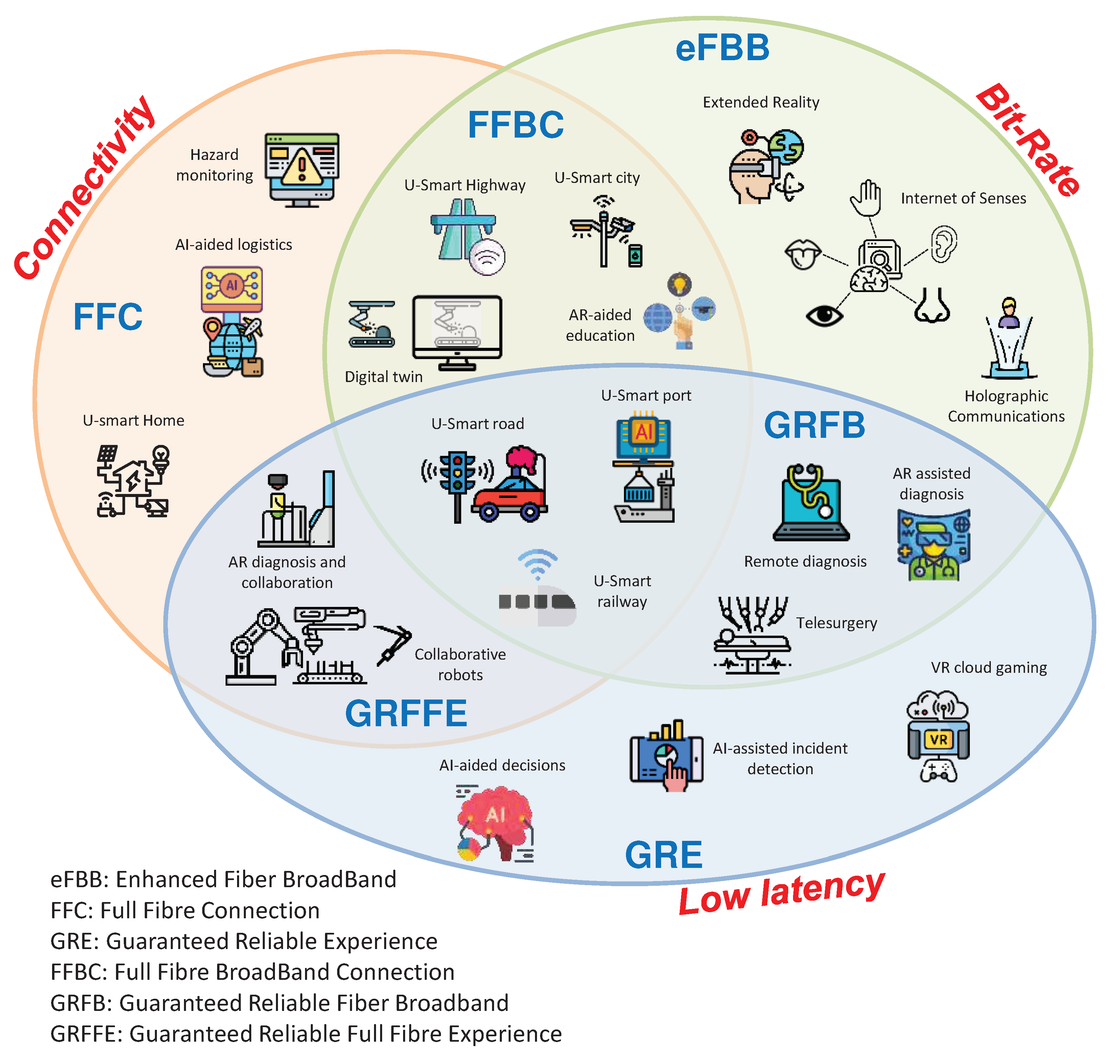
As shown in Figure 1, the network evolution is service driven, and the network operators and service providers continuously try to introduce “fresh” services to the users in order to capitalize their investments on their network upgrades/transformations. Consequently, the service needs are always increasing with time. As in this paper we focus mainly on F6G, we tabulate a list with the most representative categories and services for the F6G ecosystem (Table 1). We classify the services into six categories based on three key requirements which are bandwidth, fiber density and latency. Three categories require only one of these requirements to be met, in order to operate without disruptions, and are named Enhanced Fiber BroadBand (eFBB), Full Fiber Connection (FFC) and Guaranteed Reliable Experience (GRE) [5]. The main key requirement for each category is high bit rate, high densification, and low latency, respectively. Further, three more categories require a combination of the aforementioned three key requirements and are named as Full Fiber BroadBand Connection (FFBC), requiring both high fiber density and high bit rate; Guaranteed Reliable Fiber Broadband (GRFB), requiring both low latency and high bit rate, and; Guaranteed Reliable Full Fiber Experience (GRFFE), requiring both high fiber density and low latency. It is worth mentioning, that some services may require all the three key requirements to be met concurrently, as they need to collect bandwidth-consuming signals and data (e.g., video) from various network points in order to process them in real time and inform the respective element in order to make a decision. Indicative services for this category are ultra-smart ports, airports, railways as well as autonomous truck and taxi-fleets. Our vision on the F6G ecosystem incorporating the six service categories is pictorially described in Figure 2.
Another classification which can be made regarding the F6G services is based on the domain of operation. The first domain includes I4.0 services, such as digital twins, automated operations in harsh environment, collaborative robots (cobots), Augmented Reality (AR) and AI synergy with cloud computing which aims to improve the quality of decisions on the production line. These services require high bandwidth, low latency, high reliability and medium fiber density in order to operate efficiently. The second category includes entertainment/communication services, such as holograms, immersive extended reality and internet of senses. There is a dissimilarity regarding the requirements of these services (e.g., holographic communications and extended reality require high bit rate and low latency while the internet of senses shows more relaxed needs on latency and bitrate). The third category includes ultra-smart transportation, and can be introduced in various types of mediums, such as ports, airports, city roads, highways and railways. Safety is one of the most important requirements here, but reliability, sufficient availability, high bandwidth and low latency are also a must. The fourth category includes e-health services, such as Telesurgery, AR field medical support and remote areas diagnosis/consultations which mandate low latency and very high reliability. In the fifth category, the AR-assisted remote education requires increased bitrate in order to provide a high level of interaction between the students and the teachers. In addition, low latency is required in order to interact in real-time. In the final category, various safety-related services can be found, such as health hazard monitoring and AI assisted incident detection which depending on the target monitored metric may require low latency (e.g., detecting an imminent threat), or high connectivity (e.g., monitoring and sensing several places concurrently for health hazards).

2.3. The indispensable network transformation in order to realize the F6G vision

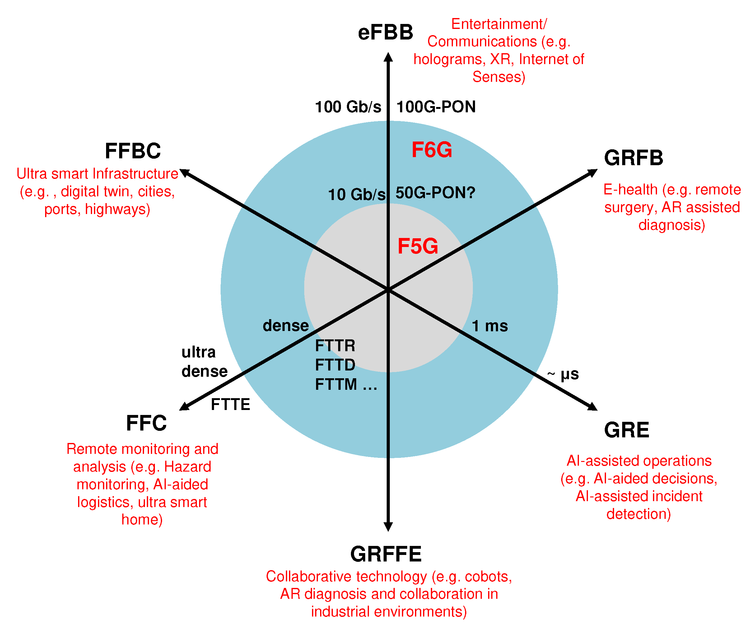
In order to elaborate on the requirements of each of the six categories of services presented in Figure 2, we illustrate how F6G extends the key quantities when it is compared with F5G (Figure 3). Of course, there are additional critical requirements which need to be satisfied and are usually service-depended, such as security, operational efficiency, spectral utilization, cost/power efficiency [5], jitter etc. however, in this work we are focusing on the three key metrics which are latency, bit rate and fiber density as at least one of them is critical for any F6G service. Figure 3 highlights that first, the introduction of a fresh Passive Optical Network (PON) standard is required in order to reach data rates of 100 Gb/s and beyond in the access domain and support bandwidth critical services. Further, a new densification strategy needs to be adopted in order to realize Fiber to the Everything (FTTE) which aims to integrate into a single network entity all “Fiber to the X” concepts that are expected to be introduced during F5G (such as Fiber to the Home (FTTH), Fiber to the Office (FTTO), Fiber to the Room (FTTR), Fiber to the Desk (FTTD) and Fiber to the Machine (FTTM) [6]). At the same time, this densification will aid integrating fixed and wireless networks, leading to a major network transformation through which the network will be able to support concretely the demands of both wireless-based and wired-based services. Regarding latency, the F6G infrastructure is expected to advance significantly compared with F5G, in order to support services with very low latency requirements, especially those of the industrial sector, which can be down at the order of some tens of μs [7,8,9,10]. In order to attain all these very strict requirements, there is a strong need for the network/service providers to upgrade their current network infrastructure both at a component and network level as well as to make their network fully automated in order to perform fast and accurate decisions at a μs timescale.
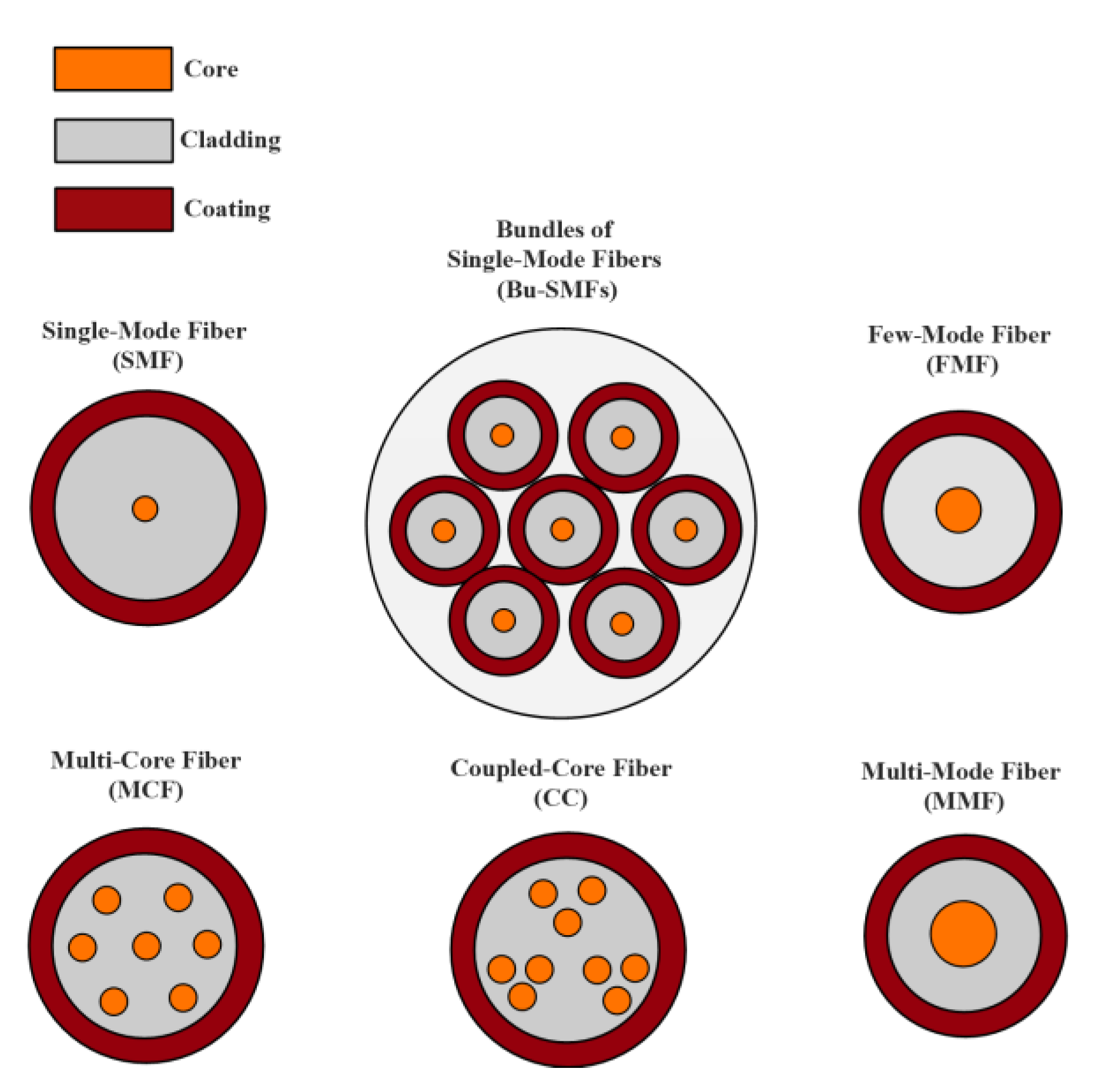
Towards this target, this work proposes in the next three sections various directions and solutions which can aid to underpin the F6G services in a cost and energy efficient way. Indicatively, a significantly larger spectrum needs to be allocated, which can be realized either by exploiting all five low attenuation bands of the optical fiber or by performing SDM, which in essence means data transmission through bundles of fibers, multi-core fibers, multi-mode fibers, few-mode fibers and/or their combination [11,12,13]. At the same time, very high-capacity switches need to be installed and operate at very high bit rates (per channel) [14,15,16,17]. Further, ultra-fast optical switching will be a must in order to attain as low end-to-end delay as possible by eliminating delay [7,10]. In order to reduce the overall cost and power consumption, novel all-optical transceivers need to be deployed, e.g. without the need for cumbersome modules such as electronic Digital to Analog Converters (eDACs) while the introduction of wavelength band converters and comb generators will assist in removing the electronic conversion which can lead to a lower end-to-end delay. Finally, a convergence between various technologies and methods such as those in 6G and F6G as well as an all-encompassing integration is required. This conversion will transform the network into a sensor, communicator and super-computer enabling it to automatically make AI-based decisions.

3. Photonics-based subsystems for all-optical processing

In recent years, innovative approaches have emerged to address the challenge of efficient scaling of the bit-rate of the transceivers (TRx), to support the various network segments per their specific needs. From a cost and power consumption perspective, the TRx requirements of the optical access network in the 5G/6G era, are quite distinct from those of core networks, and the emphasis is on further reduction of cost/power consumption of short-reach systems. Another significant feature of state-of-the-art TRxs is their capability to dynamically vary the bitrate and have them tailored to variable service demand. This feature is beneficial for network operators, as it provides significant savings in cost and energy. Hence, TRx breakthroughs enabling to unlock bitrate up-scaling, energy/cost-efficiency and agile programmability of parameters such as modulation format or baud-rate, are desirable. To attain these objectives, TRxs for fiber-optic transmission have been extensively developed for long-haul transmission, wherein the key objective is capacity × reach maximization, whereas cost and energy efficiency are deemed secondary requirements. The energy-efficiency challenge, in particular, emerges as a key barrier precluding straightforward migration of high-bit rate TRxs from long-reach links, to short-reach 5G/6G and cloud networks / datacentre interconnects.
A major driving force boosting TRxs capabilities over the past few decades has been the tremendous advance in electronics. Unfortunately, porting those advances to the environment of short-reach communication is now proving difficult, as silicon technology approaches its energy-efficiency limits, no longer able to keep supporting the energy demands of the ever higher sought performance. In particular, state-of-the-art implementations of ultra-high-speed optical transceivers, used in coherent long-haul systems for generating and detecting Tb/s signal constellations, are based on power-hungry electronic Application-Specific Integrated Circuits (ASICs), used platforms to implement electronic DACs (eDAC), electronic ADCs (eADC) and Digital Signal Processing (DSP) functionalities. At the transmitter side, eDACs are key interfaces converting the signal from the digital to the analog domain. In high-speed optical transmitters, the state-of-the-art techniques for digital-to-optical (D/O) transduction typically comprise power consuming and costly eDAC-based data-conversion, followed by analog optical modulation. As eDAC technology is becoming more expensive in both cost and energy, next-generation TRxs are highly challenged to sustain upscaling in speed, while keeping power dissipation at bay. In particular, the rise in the pJ/b figure-of-merit is a major bottleneck in TRxs employing eDAC/eADC technologies. Therefore, innovative approaches are in high need, to enable advancing the rates to as high as 10 Tb/s per TRx, at the lowest performance/capacity penalties.
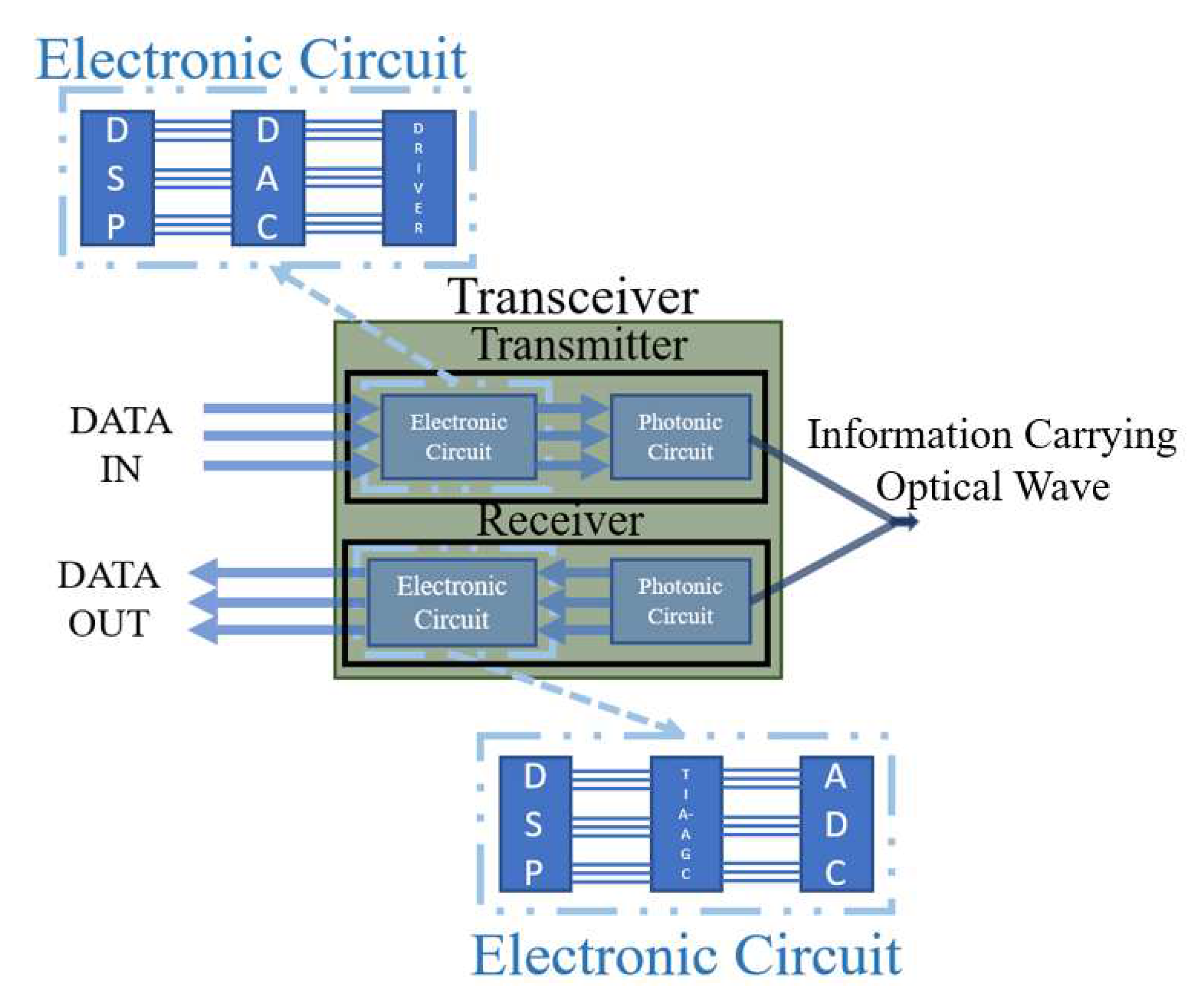
Aiming towards that objective, we commence by inspecting the transmitter and receiver structures (Figure 4) which comprise a main electronic section providing multiple essential functionalities. First, the electronic circuit in the transmitter processes the information bitstream in the digital domain, performing various operations, such as error-correction, signal mapping, spectrum shaping, pre-distortion, etc. Then, via a D/A converter (eDAC) typically of the current-steered type, followed by a transimpedance amplifier (TIA), the digital signal is transduced to voltage analog domain in order to drive the optical modulator. On the receiver side, following the optical front-end, a TIA with automatic gain control feeds an A/D converter (eADC) transducing the signal to the digital domain for Digital Signal Processing (DSP). The DSP ‘engine’ comprises building blocks such as polarization demultiplexing, carrier frequency, phase recovery, IQ imbalance compensation clock recovery, adaptive equalization, data decoding (slicer), and error detection and correction decoding; in overall compensating for distortions and mitigating/correcting errors that arise due to the physical layer impairments along the transmission link. In both Tx & Rx sides, the ultra-high-speed ADC/DAC and DSP functionalities, realized on state-of-the-art ASICs are bandwidth-constrained and turn out extremely power-hungry, imposing significant scalability limitations. Averting soaring costs and power consumption of TRxs in Access and in intra-Data Center Interconnection (DCI) networks is a particularly challenging task put forward to the research community, requiring creative approaches to enable conceiving novel efficient solutions, in light of worrisome models predicting that electricity use by information and communications technologies could exceed 20% of the worldwide electricity consumption by 2030, with data centers using more than one-third of that [18]. Therefore, solutions to increase or at least retain energy-efficiency, for the ever higher bit rates, are of utmost importance.
Efforts to develop low-cost/power interconnect solutions for short reach networks have been sparse, and mainly explored two directions: i) all-optical DAC/ADC implementations that reduce the use of electronic DACs/ADCs [19], and ii) all-optical implementation of coherent receivers as efficient alternatives to the power-hungry electronic DAC/ADC/DSP-chip functionalities [20]. It is worth mentioning that in short reach interconnects, whereat we are mainly focused, link lengths are constrained to less than 20-50 km for 5G/6G fronthaul and access networks, and less than 2 km for intra-data center interconnects, however, the bit rate can still scale to high numbers, e.g. to some hundreds of Gb/s. In these domains, less costly methods are usually employed; this is why Direct-Detection (DD) optical interconnects have been widely utilized in such short reach interconnects, heretofore. However, besides Intensity Modulation (IM)-DD systems, the option of adopting coherent detection-based transceivers in shorter reach networks has been investigated with the aim to facilitate scaling up bit-rates while reducing energy-per-bit, where according to conventional wisdom, many functions employed in the DSP-chips of long-haul-oriented transceivers addressing dispersion and non-linearities of the optical fiber (which are absent or less prominent in short-reach links), can be removed, in order to mitigate the cost and power consumption bottleneck of the electronic circuitry.
In the following subsections of this section, we survey all-optical solutions to be harnessed to tackle the upcoming bottlenecks of increased power consumption and cost that electronics are subject to (subsection 3.1). Subsequently, we describe how analog-to-digital and digital-to-analog conversion can be implemented using mainly photonic technology (subsections 3.2 and 3.3). Finally, it is suggested that research in these two systems fits within the framework of the wider domain of ‘reconfigurable photonics’, showing use cases potentially enabling lower cost and lower power consumption (subsection 3.4).

3.1. All-optical coherent & simplified coherent solutions: Challenges & Opportunities

Recently, interest has arisen in the implementation of analogue-based coherent receivers to substantially reduce the power consumption at the receiver side, by eliminating the power-hungry DACs/ADCs and DSP. Along these lines, several new techniques have been proposed to implement spectrally-efficient and low-power consumption links, based in particular on Stokes vector detection, Self-Coherent (SC), and Krammers-Kronig (KK) techniques. Self-coherent systems have been proposed for DCI due to their promise of offering low complexity, higher spectral efficiency, and increased dispersion tolerance [21], enabling partial attainment of the advantages of fully-coherent detection. Several DSP-based approaches have been proposed to linearize self-coherent systems (mitigating the signal-to-signal beat noise component), however, the KK algorithm turns out the most effective. Stokes vector detection can exploit up to three degrees of freedom and circumvent the local oscillator (LO) required in coherent systems, but it is also based on power-hungry ADCs and DSP [22]. A quantitative comparison of four low cost/power consumption TRxs for short reach interconnects is presented in the following table.
Table 2. Comparison of various parameters of four low -cost/-power transceiver schemes for short-reach transmission [23].
PAM-4 Duobinary DP-QPSK KK
LO requirements DFB DFB Electrical PLL None
Tx complexity MZM MZM / DML I/Q modulator Quad MZM for SSB
DSP at Rx NO NO NO YES (Heavy)
Spectral efficiency (b/s/Hz) 1 1.1 2 5
Filter-less networks YES YES YES NO
Signaling rate 25 Gbs/s/λ 25 Gbs/s/λ/pol 112 Gbs/s/λ/pol 224 Gbs/s/λ/pol
Reach 20 km 20 km 20 km 100 km
Rx sensitivity (at FEC limit) -17 dBm -37.3 dBm -26.5 dBm 24 dB OSNR
Application Intra-DC Intra-DC Short reach Inter-DC
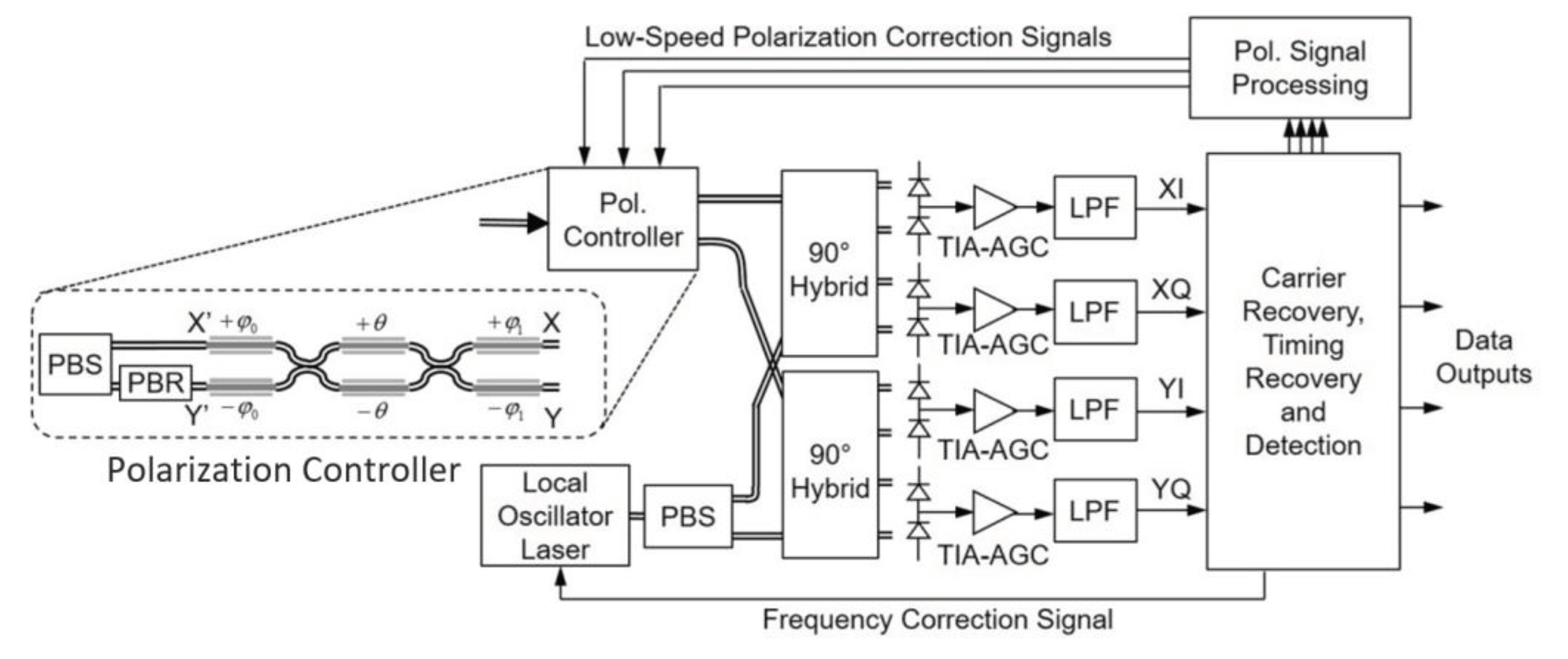
A notable alternative, the all-optical receiver, has been initially presented in [23] (see Figure 5 for its high-level design), indicating the possibility to replace the DSP chip with an all-optical analogue front-end that can achieve most of the required functionality.
The novel required Rx Blocks of this scheme are:
Analog optical carrier phase recovery utilizing an Optical Phase-Locked Loop (OPLL) based on a low-linewidth Laser [20,24], to optically decouple the two I and Q quadratures, and
Analog optical polarization demultiplexing circuit [25], decoupling all-optically the two signal polarizations.
The OPLL, could be implemented, at a bandwidth of ~10-100MHz, based on a high-bandwidth photodetector and a low-linewidth semiconductor laser, operating the local oscillator laser as a Current Controlled Oscillator (CCO). The Analogue Polarization Demultiplexing (PolDMUX) circuit block, depicted in Figure 5 in the polarization controller inset, consists of a cascade of a several 2x2 matrix stages and it is implemented based on directional couplers and phase modulators (PMs), as it experimented in [21]. It is noted that slow (~10kHz rate) precise tuning control of the phase alignments of the PMs in the cascade is required as an essential enabler for the practical polarization demux functionality of this block to which we refer as Analog Optical Signal Processor (AOSP). Due to the all-optical nature of signal processing in the 10KHz-100MHz building blocks of this transceiver, which are transparent to the ultra-high-speed optical signals modulated onto the light flowing along it, the efficient operation of the AOSP polarization demux is essentially independent of the baud-rate, hence the supported bit-rate is scalable to > 800 Gb/s rates per wavelength/space lane. Moreover, multiple optical wavelengths may be served at once (polarization demultiplexed together by a single AOSP) to further scale the offered capacity. The AOSP is still followed by ADCs (slicers), albeit at much reduced Effective Number Of Bits (ENOB), and the DSP is much reduced in cost, footprint and power consumption, as the XY polarizations and IQ quadratures are effectively decoupled ahead of the four ADCs. Other receiver operations such as timing recovery and detection may be performed with a high-speed analog electronics stage using conventional clock and data recovery (CDR) techniques. Alternatively, these functions may be relegated to the scaled-down DSP.
Figure 5. Block diagram of DSP-free coherent receiver (PM-QPSK) based on AOSP [26].
Preprints 76390 g005
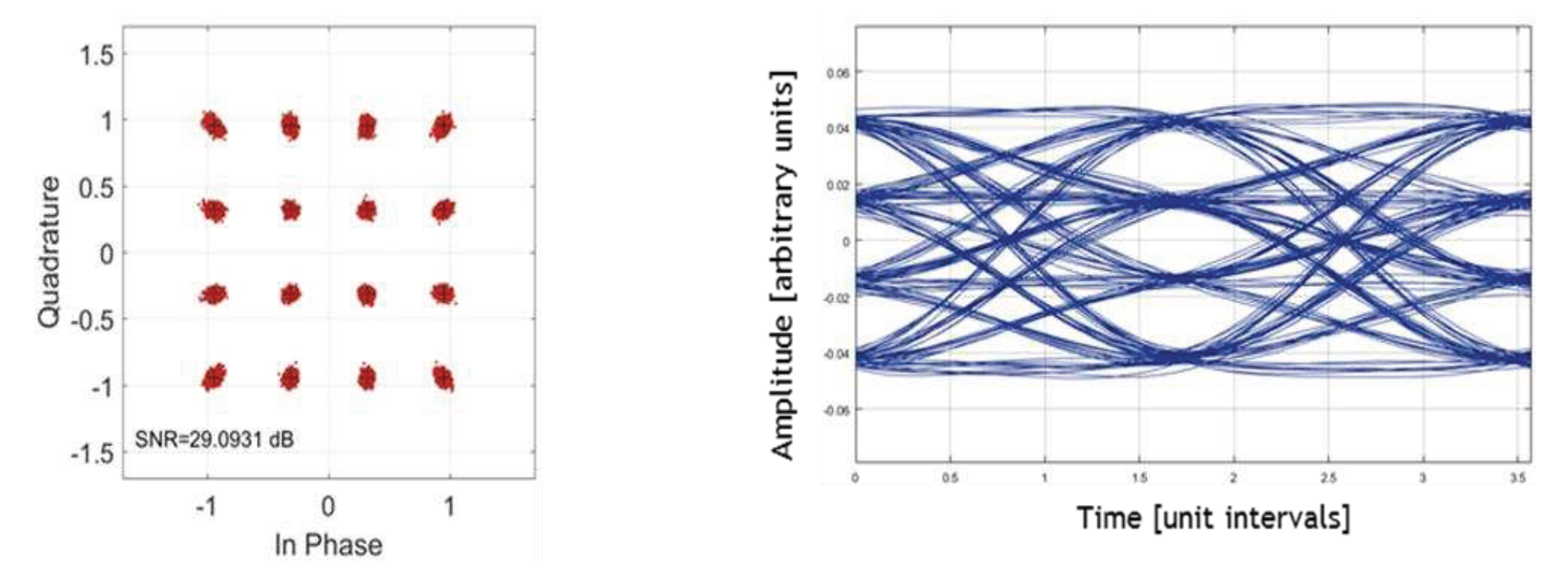
For basic proof of principle feasibility purposes, the operation of such AOSP receiver has been demonstrated via preliminary simulations and the results are shown in Figure 6. In this particular example, the operation at an aggregate rate of 400 Gb/s was considered [23]. In the simulation platform, the AOSP was constructed by considering a low-linewidth local oscillator laser and a cascade of discrete Mach-Zehnder Modulators (MZMs) and PMs for the Pol-Demux, which is not as effective as in the case where integrated elements in a Photonic Integrated Circuit (PIC) are employed. Following the all-optical AOSP-based polarization demultiplexing and phase/frequency recovery operations, the four coherently recovered analogue lanes Ix, Qx, Iy, Qy, display clear bipolar Pulse Amplitude Modulation 4 (PAM4) eye diagrams which are detectable using conventional CDRs (based on all-analogue electronic symbol timing recovery & 4-level slicing implemented in merchant Silicon circuity). These initial simulation results at 400 Gb/s [23], are significant, as they validate the feasibility of the all-optical analogue signal processing based coherent transceiver.
The aforementioned all-optical solutions, besides the sufficient transmission performance, can also scale-up the capacity capabilities in order to meet the ever-growing traffic demands of the coming decade. Furthermore, they can serve as important solutions for optical interconnects in datacenters and 5G telecom infrastructures, which are the network domains wherein the cost (measure in $/Gbps) and power consumption (W/Tb/s) must be further reduced [23].
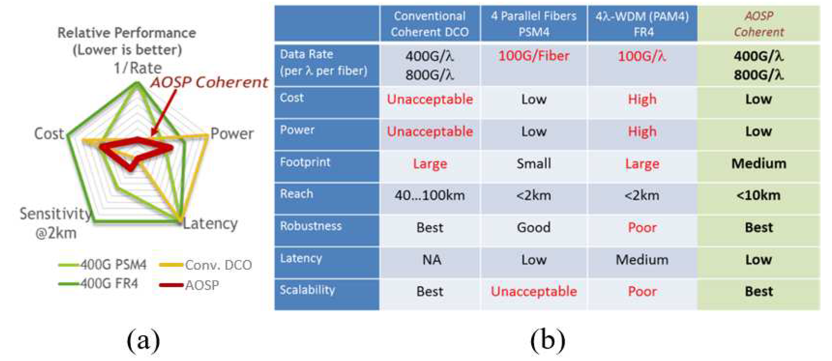
Figure 7, presents a high-level comparison between the AOSP based transceiver and other popular transceiver designs for 400 Gb/s interconnects. Evidently, the cost and power consumption using conventional coherent solutions are prohibitively large for such applications. A straightforward solution could consist of the combination of parallel fibers exploiting lower performance transceivers in order to achieve the desired capacity. Unfortunately, the scalability of such idea, once benchmarked against alternatives, is limited by the number of fibers that can be deployed in parallel. Another potential solution is Wavelength Division Multiplexing (WDM), however WDM is constrained in cost and power consumption due to the high complexity of deployment. As a consequence, it is becoming evident that for short-reach applications (below 10 km) the AOSP transceiver may be a competitive option as it concurrently addresses the desirable characteristics of low cost and power consumption, high data rate, low latency, high scalability and reach of up to at least 10 km.
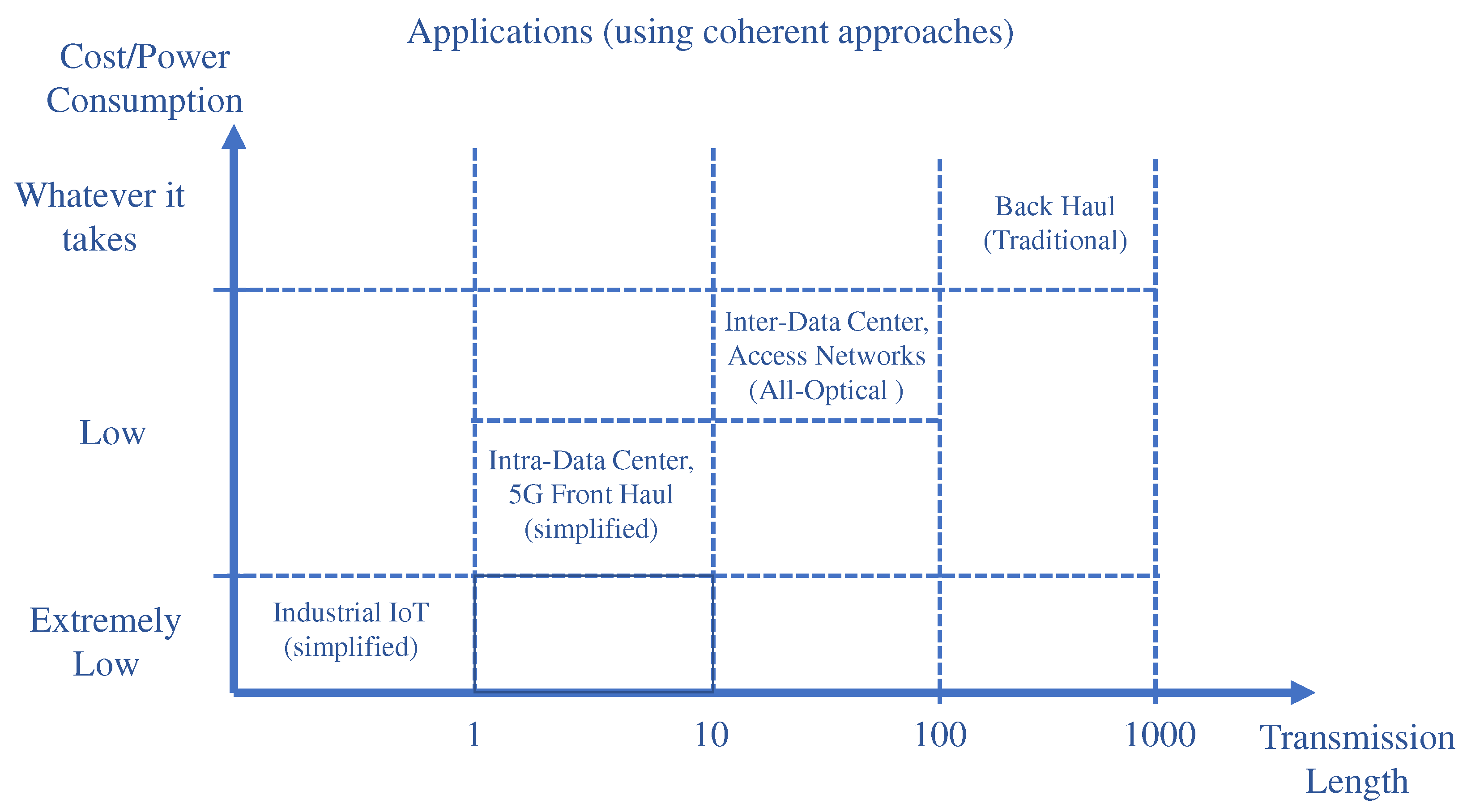
Other notable options are classified in the category of ‘simplified coherent’ solutions. These solutions entail various tradeoffs between the extremes of direct-detection and coherent detection, exploiting both the amplitude and the phase of the optical signal to increase the transmitted data rate, albeit with lower complexity compared with conventional coherent transceivers, e.g. comprising a smaller number of optical elements. The main advantage in coherent technology is the benefit from up to 4-times higher bit-rate, while keeping transceiver cost and power consumption at bay. To achieve this goal, new all-optical techniques are envisaged [27,28,29]. Using these alternatives, the cumbersome DSP components are no longer required. These techniques target extremely low-cost applications where the requirements cannot be simply met via using direct detection techniques, whereas the cost and power consumption of fully-coherent solutions would be prohibitive, whereas the coherent performance would be an ‘overkill’.
In this category of solutions, Erkilinc et al. in [27] proposed a single polarization scheme that incorporates a polarization-time block-code signal, circumventing polarization tracking, driving a dual-polarization modulator at the transmitter. In this context, both intradyne and heterodyne architectures have been investigated and resulted to massive simplification of the receiver side, discarding polarization rotators, beam splitters, two balanced Photo-Diodes (PD) as well as ADCs. Next, Cano et al [28] adopted another simplified version, first introduced by Kazovsky et al. [29], using a 3x3 coupler followed by three single-ended PDs and 3 ADCs for the intradyne reception. The main advantage of this solution is the polarization scrambling technique [30], attaining polarization-independent detection avoiding polarization tracking devices at the receiver. The third approach by Ciaramella [31] utilized polarization-independent reception with a polarization beam splitter (PBS) and a symmetric 3x3 coupler followed by three single-ended PDs. The 3x3 coupler incorporated the intermixing of 3 signals: a) one horizontal signal b) one vertical polarized signal and c) the incoming signal. The horizontal and vertical signals are output by the polarization beam splitter. In this architecture, ADCs and DSP can be completely removed; therefore, only On Off Keying (OOK) or PAM4 signal can be detected by the receiver. The most recent work in the literature is called quasi-coherent [32,33], also classified in the category of simplified coherent approaches. Here, the signal and LO are mixed using a coupler. Then passing them through a PBS, the two resulting optical signals are fed into two PDs and next, by performing envelope detection, they are inserted into the electronic amplifier. Based on these aforementioned techniques, we conclude that dual-polarization schemes or Quadrature Amplitude Modulation (QAM) formats can be dispensed with under certain conditions, for the sake of minimization of optical and/or electrical components, albeit the reduced data rates. That is why these coherent-like approaches are best suited for extremely low-cost and low-power consumption solutions in short-reach applications, but do not typically qualify for either long-haul transmission or for high-end (inter) datacenter interconnects.
It is for this reason, that new coherent approaches emerge in order to cover the white areas of optical communication market. Based on the complexity which directly impacts the cost and power consumption, Figure 8 maps the different options with the network domain where they can be applied.

3.2. Photonic ADCs: Challenges & Opportunities

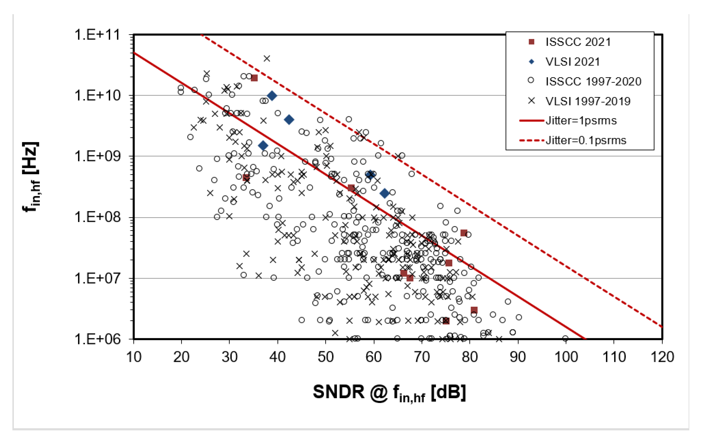
A tremendous amount of research has been conducted on Analog to Digital Conversion from the beginning of modern telecommunications. The reason is apparent: the information to be exchanged among the users via the Internet is predominantly, almost exclusively, digital. Although research is focused on both electronic and photonic realizations of ADCs, heretofore only the electronic ones have been commercialized. More specifically, due to the steady decrease in transistor size (technology node), commercial solutions have exclusively focused on development on the electronic option: eADCs. Unfortunately, in the last 10 years, the transistors’ speed and size have started approaching their limits [34]. In particular, Murmann's survey for 2021 [34] highlights that energy consumption and jitter are the main bottlenecks which have mainly arisen from minimization of the technology node. Figure 9 shows Energy per Nyquist sample as a function of Signal to Noise plus Distortion Ratio (SNDR) which is one of the most well-known FoM metrics that evaluates the performance of an ADC. SNDR is measured when the frequency of operation is set to Nyquist Rate / 2. In this figure, the lines for Jitter=0.1 psrms/1 psrms designate the performance that a fictitious sampler with only the specified jitter numbers (no other nonidealities such as quantization noise, etc.) would achieve.
On the other hand, accurate Analog to Digital (A/D) conversion of wideband multi-GHz signals has always been a problem as the use of eADCs is far from optimal and not sufficiently scalable looking forward. The reason is that digitizing analog signals in the range of 100 GHz and beyond is practically impossible because of the lack of electronic devices which can sample the input signal with sufficient low aperture jitter at this rate, as it is shown in Figure 9. These facts kept the research of photonic ADCs active for almost 30 years, however, without yielding a practical realization at sufficient SNDR.
The origins of photonic ADCs date back to 1970 when Siegman and Kuizenga [35] were working on optical sampling of Radio Frequency (RF) signals notwithstanding that the different main target of that work. Photonic ADCs can be classified into four broad categories as per Figure 10 [36]: In particular, photonic-assisted ADCs use optics in order to replace the track-and-hold operation on the RF input signal, perform both sampling and quantization in the electronic domain. Photonic sampled ADCs and photonic quantized ADCs use photonic technology to sample or quantize the signal (but not both), respectively. The combination of sampling and quantizing the signal with photonics is a different category were that enables the optical sampling of intensity, angle.
As the range of the different approaches for constructing a photonic ADC is huge, the most useful category is the one aiming to overcome the most significant bottleneck of high-speed eADCs. That category is the photonic-sampled ADCs that overcomes the electronic jitter limitation. A general overview of photonic ADCs can be found in the excellent review by Valley [36]. Heretofore, there have been just three implemented and tested State-of-the-Art photonic-sampled ADCs, based on a common fundamental principle of operation. The first one was proposed by a group of researchers at MIT in 2012 [37], whereby they implemented a discrete time-to-wavelength mapping approach (an approach first proposed by Yariv in [38]). The second alternative resulted from a collaboration of researchers from Rohde & Schwarz and IHP in 2017 [39], which demonstrated a monolithically integrated time-interleaved topology to relax the timing constraints at the highest sampling rates. The third and most recent one was proposed by the Institute of Integrated Photonics of Aachen University [39], demonstrated for two monolithically integrated topologies; one based on a time-interleaving whereas the second one was based on frequency interleaving.
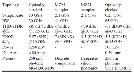
Although the target here is not to elaborate on the principle of operation of these implementations, we discuss the most important aspect, namely the optical sampling of the RF signal, first proposed by Taylor in 1978 [40]. The main components of an optically sampled system are shown in Figure 11 and comprise a stable pulsed laser, an optical modulator and a detector/integrator. The basic concept is that the ultra-short pulses of the laser actuate the modular over an ultra-short and ultra-stable (low-jitter) time-window, such that the average amplitude of the analog signal over that window, an excellent approximation of a point-sample, is mapped on the amplitude of the optical signal. This mapping of the amplitude is converted into electrical variation by the photodetector and eventually quantized in the electronic domain (thus the sampling is performed by optics, the quantizing is electronic). The most significant advantage is that the overall jitter induced on the laser pulses is much smaller compared with the jitter created in its electronic counterpart. For clarification, the sampling rate is just the Mode-Locked Laser (MLL) pulse repetition period. As demonstrated in [37], with a single laser several repetition periods can be implemented by adding also a multiplexer, a dispersive fiber and a demultiplexer. A comparative analysis for various options of the optical sampling process is summarized in Table 3.
In Table 3, a trade-off between the sample rate and the bandwidth of the optical sampling processes for RF signals is evident across these four alternatives. Alongside this trade-off, it should be pointed out that different processes to manufacture the PICs have been employed. Both bipolar complementary metal–oxide–semiconductor (BiCMOS) and silicon photonic integration may be considered. All four variants have successfully implemented a photonic-sampled ADC, with the latest option exceeding 60 GHz bandwidth and achieving the lowest power consumption and die area. These four variants validate the concept of photonic ADC and establish its great potential to enable systems aiming to process signals in the microwave region with sufficient accuracy, made possible by the sampling photonic technology.
In conclusion, we deem it important to point out that as a first step, the major bottleneck of high-speed ADCs may be eliminated based on photonic technology, exceeding the performance of an electronic counterpart. The next step towards achieving a fully optically-enabled ADC is to conceive a feasible method that implements photonic quantization. Although practical implementations haven't been realized yet, some photonic sampled architectures through optical quantization architectures hold promise to exceed their electronical counterparts [41], as well as to reduce power consumption due to the use of optical elements. Nevertheless, a significant amount of additional work lies ahead along the road towards realizing an all-optical ADC with reduced power consumption. Moreover, the photonic ADCs surveyed above have electronic inputs and outputs. A worthy future objective would be to establish the feasibility of an oADC with optical input (carrying the information modulated signal) and electronic digitized output, embedded in a future all-optical polarization and IQ demultiplexing front-end of a coherent receiver, in order to pave the way for truly all-optical low-energy consumption systems.

3.3. Photonic DACs: Challenges & Opportunities

Electronic Digital to Analog Converters, abbreviated as eDACs, are key interfaces that convert the signal from the digital to the analog domain. In high-speed digital optical transmitters, the D/O translation typically comprises costly and power consuming eDAC-based data conversion, followed by analogue optical modulation. In a conventional optical link, eDACs are used to drive multilevel analog signals into the optical modulators. As mentioned earlier in this chapter, from the viewpoints of performance, energy efficiency, complexity and cost reduction, it would be advantageous to adopt direct D/O conversion, and eliminate the eDAC intermediaries. This would be particularly useful with regard to ultra-high-speed photonic interconnects, as eDAC technology is even more expensive and is becoming increasingly challenging to keep scaling up in data rates, while keeping power dissipation in reasonable levels and maintaining the required ENOB performance.
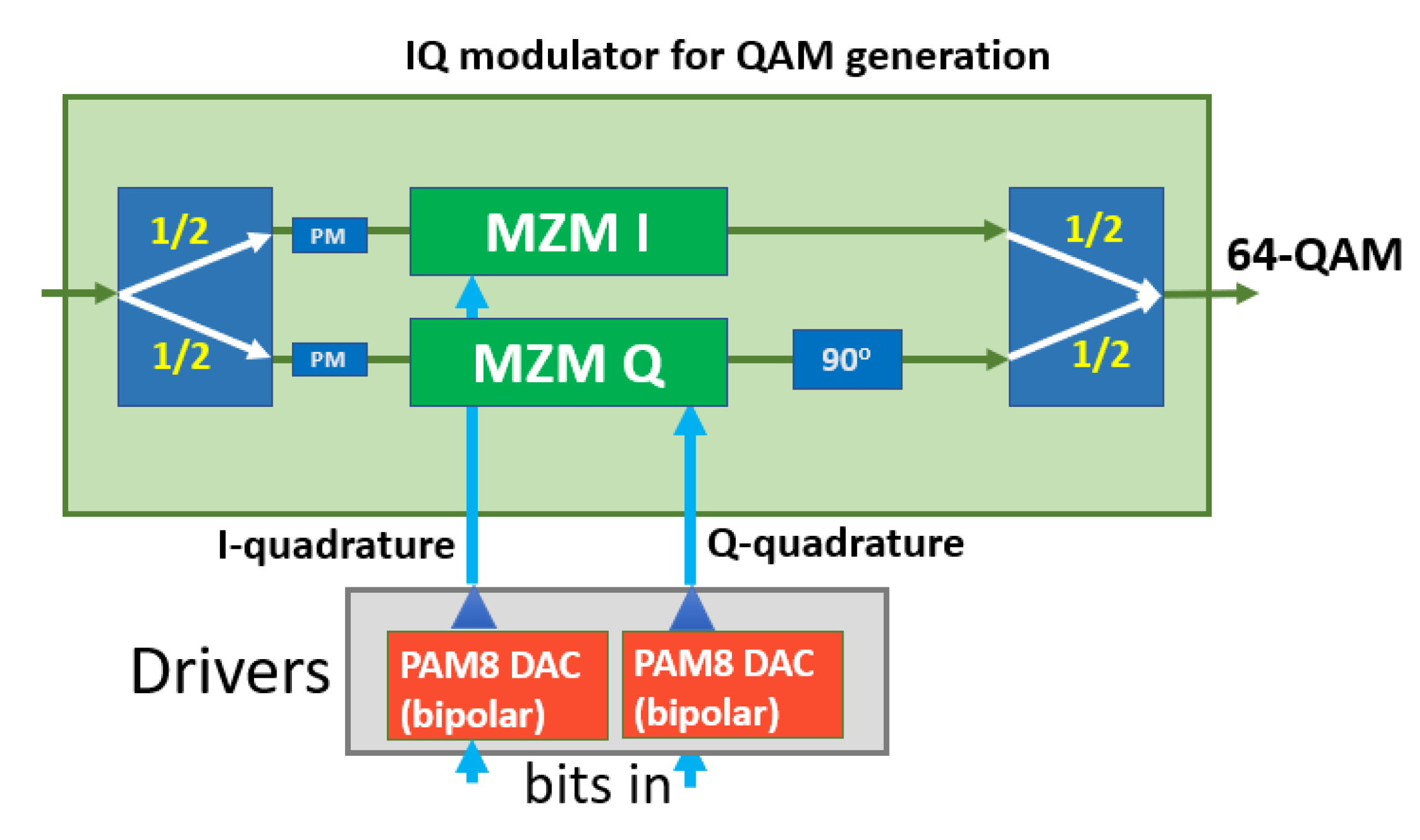
To introduce optical to digital conversion, let us first review the conventional way of generating multi-level optical signals. For decades, IQ modulators, generating optical constellation signals remained the same, e.g the case of 64QAM is illustrated in Figure 12. The light split to the two parallel optical paths is modulated using a pair of MZMs. Each MZM modulates the Continuous Wave (CW) optical signals according to the electrical voltage applied to its electrodes. As a consequence, for quantized electrical voltage levels applied to the MZM electrodes, quantized optical levels are generated (and are relatively phased 90o along the two parallel paths). However, the bandwidth of the entire transmitter is limited by the lowest bandwidth of either the DAC in electronic driver or the MZM electrical to optical modulator transducer.
In order to scale-up the capacity of a single-lane point-to-point optical tributary, one can either increase the baudrate or adopt formats with higher spectral efficiency. These solutions require either faster electronics or more complex DSP in the Rx. Either way, both options entail increased cost and power consumption. In addition, as the silicon technology is approaching its physical limits, the use of faster electronics no longer seems a viable solution in terms of its upscaling rate, which is no longer able to keep up with the data rate scaling roadmap. This is why one of the key goals of the research community is the reduction of the energy-per-bit by conceiving a new optical transceiver architecture able to attain direct digital to optical domain conversion, the optical DAC (oDAC), eliminating power-hungry electronics, specifically doing away with conventionally expected future eADCs featuring 3 or more bits, given their scalability problem in rate-vs-energy-efficiency. The oDAC will still be driven by electronic D/A interfaces, but those will be highly efficient and scalable – the drivers of the oDAC will comprise arrays of decoupled 1 bit (NRZ) or at most 2 bits (PAM4), where signal formats are relatively mature, more energy efficient, and more amenable to upscaling than higher-order ADCs that are about to be pushed beyond their limits in the upcoming optical interconnects roadmap.
Over the last decade, the research activity regarding the oDAC, has been mainly focused on 'serial' structures, that are based on partitioning the electrodes of the basic MZM (Figure 13). The so-called Segmented Mach-Zehnder Modulator (SEMZM) [42,43,44,45,46,47,48,49,50] breaks up the MZM electrodes pair along the two MZM waveguides into multiple (shorter) electrically isolated segments. Each modulation-segment amounts to an elementary 1-bit modulation gate driven by a separate binary signal. The summation of the optical phases induced by the array of 1-bit segments along the device generates a multilevel output optical signal. Accordingly, Figure 13 depicts an exemplary S = 7 segment thermometer weighted SEMZM optical structure, aiming to implement oDAC functionality. The contiguous MZM electrodes are partitioned into S segments. Each segment acts a “partial MZM” with push-pull drive. Hypothetically assuming a single segment is electrically driven (the other segments grounded or removed) we would obtain a “partial” MZM modulator with a short electrode pair, inducing just a fraction of the maximally possible peak phase modulation, as attained when all segments are active. When all the segments are modulated in unison, driven by properly synchronized binary signals, the total differential phase along the device may assume a multiplicity of values, inducing, by interference in the output coupler multiple optical amplitude (or power) levels at the device output.
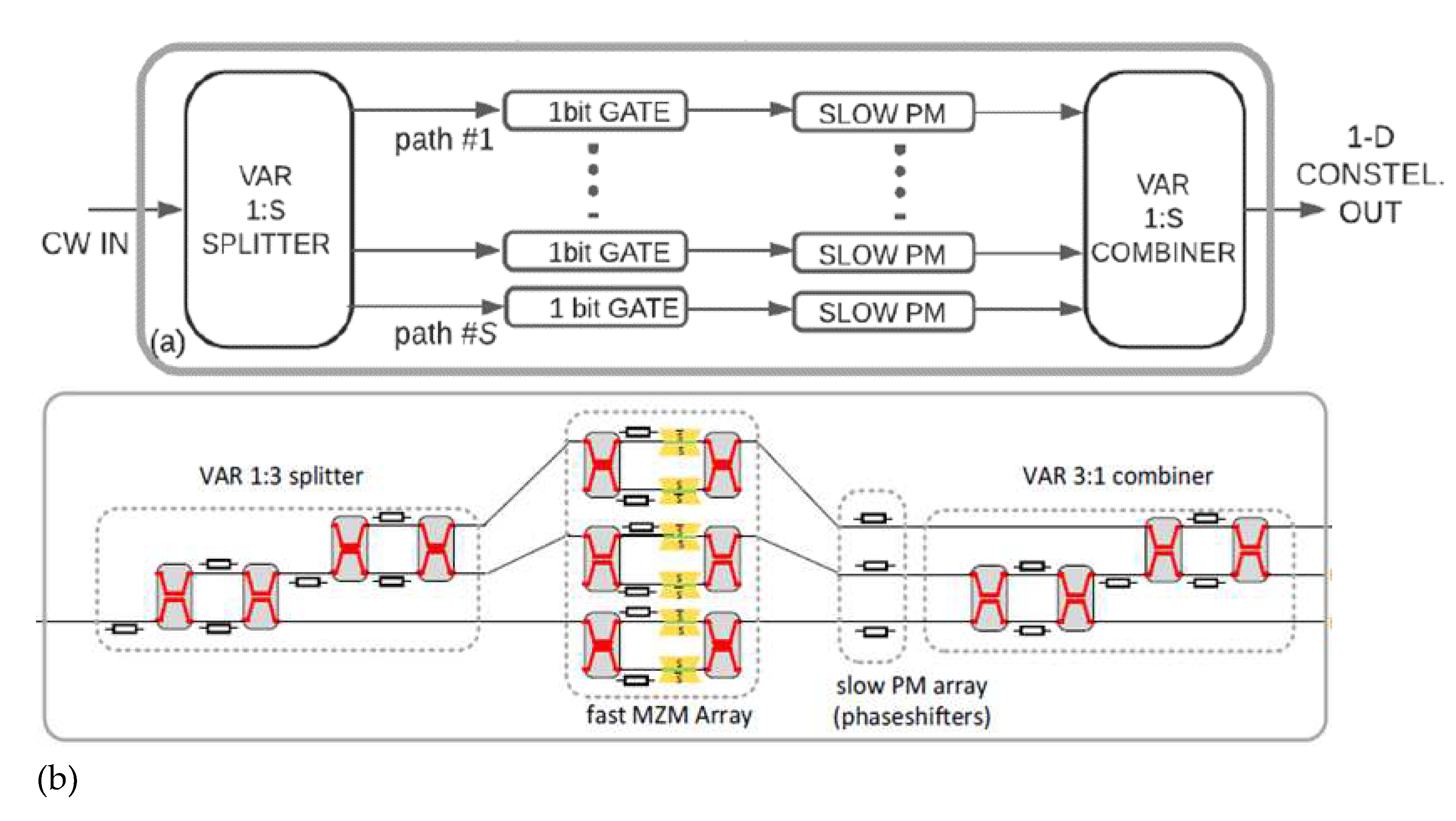
As an alternative approach, a “parallel’’ design that employs electroabsorption modulators (EAM) instead of MZMs has been also proposed in [51]. The compact size of the EAMs and their ease of integration with silicon photonics makes them a real lucrative option. However, various works examining the 'multi-parallel' oDAC functionality have been proposed, e.g. via arraying in parallel a pair of 1-bit (OOK) [51] or 2-bit (QPSK) [52,53,54,55] modulation gates, fed after splitting a common optical source, with their outputs superposed in an optical combiner. The latest and state-of-art 'multi-parallel' oDAC structure is proposed in [19] introducing an architecture which, via the combination of identical parallel paths and a variable splitter and combiner, is able to generate both direct and coherent detection constellations (Figure 14a).
The basic goal of a parallel design is to generate optical multilevel PAM signals using only binary driving digital signals. As shown in Figure 14a, in this implementation, 1-bit gates are the fundamental building blocks. These blocks either let the optical signal to pass through the specific path or block it and can be practically implemented using MZMs. Then, by adding all the optical paths using a combiner, optical signals with different amplitude levels can be generated. Figure 14b illustrates how a PAM8 generator can be implemented using this architecture. In practice, the variable splitters and combiners are identical and bit gates are put just in parallel demonstrating the high scalability of this architecture. In that aspect it's possible not only to scale the parallel paths but also the electronic PAM (ePAM) levels that drive the MZMs in order to scale the attainable data rate. It is theoretically established that using ePAM4 in each of the two parallel paths via a two-way o-DAC it is possible to scale the constellation up to optical 256-QAM [56]. Moreover, extensive analysis has been performed in [46] in order to demonstrate the significance of splitting and combining ratios to realize such a design. Also, in [46] control and calibration functionalities were added along the optical paths by inserting slow phase modulators. Accounting for mismatch in splitting or combining ratios occurring in the manufacturing processes, or due to environmental disturbances, this current design becomes far more robust compared with that of previously published work.
Other optical DAC solutions based on a) silicon ring modulators [46,47], b) III-V-on-Si electro-absorption modulated distributed feedback laser [48] and c) polarization division multiplexing [50,51] have been also proposed. The previous generations of MZM devices might not be suited for short-reach interconnects as typically large transmission line structures are required. With ring resonators, the system becomes too much dependent on temperature fluctuations and needs control systems to guarantee its stable operation. Silicon microring modulators are already implemented but they are limited to 80 Gb/s rates even with DSP both at the transmitter and receiver sides, something that contradicts the notion of the DSP-free architecture. Generally, from all the experiments demonstrated heretofore, we may conclude that although optical DAC implementations have been proposed, the results show that there is no particular implementation yielding considerably better results compared with the others. If one thing is clear, is that control and calibration of different kinds of mismatches like phase mismatches or energy mismatches will play a key role for any type of deployed modulator. It goes with a saying, that the path for reducing energy consumption and achieving better performance in the near future, acknowledges that electronics have come to their limits and the future seems to be purely optical. Although these designs are promising, the research community still seeks optimal scaling options for ultra-highspeed optical modulator based transmitters, facing multiple challenges precluding a breakthrough in these directions.

3.4. Reconfigurable photonics

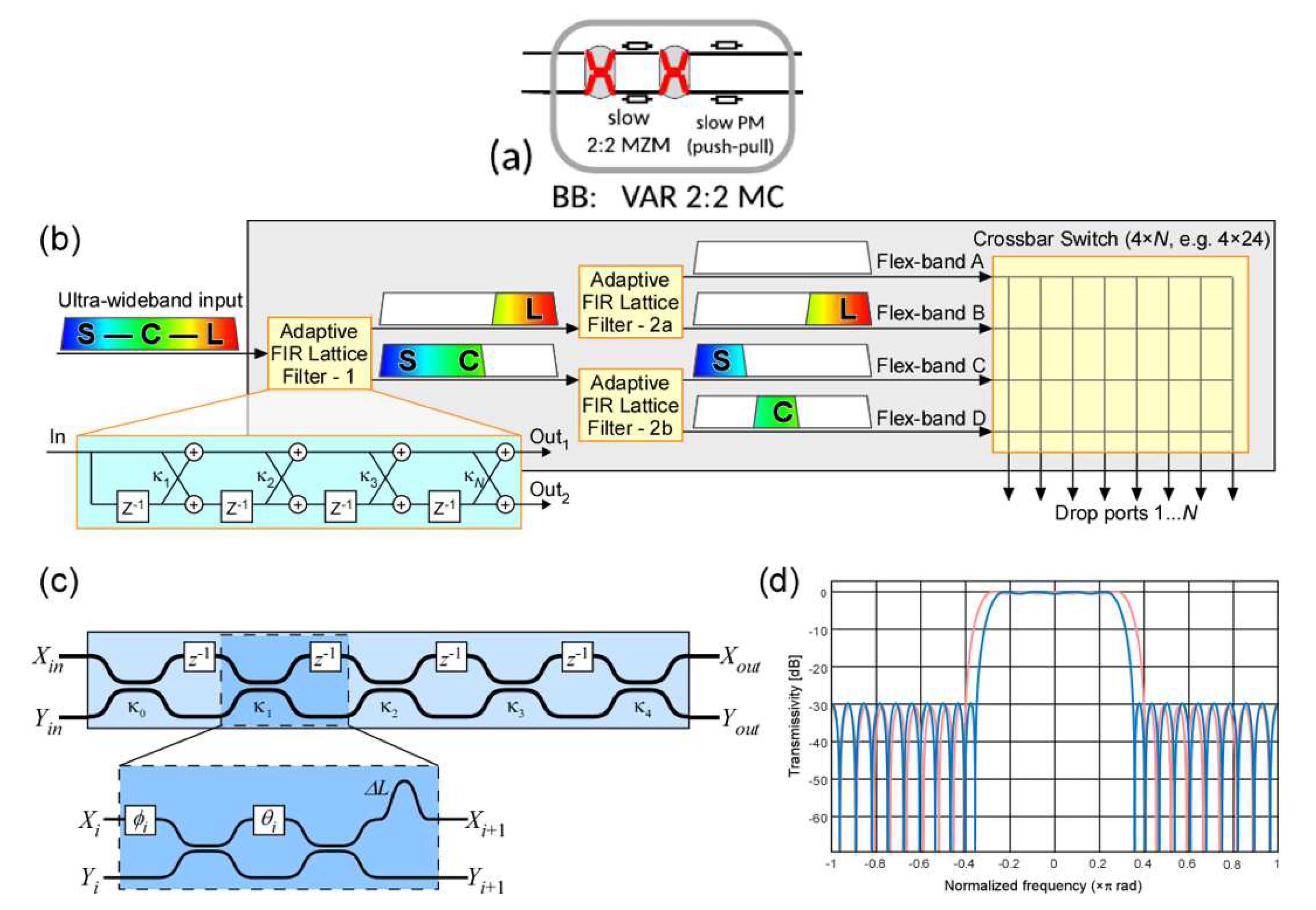
Generally, PICs have been extensively investigated as platforms for optical fiber communications. Over the past decades, the basic driving force behind creating lower-cost and more robust photonic circuits has been the increase of the data rates in order to meet the ever-increasing demand of end-users. The main objective of PICs is to process optical signals efficiently and at low latency, over a low-cost and low-power platform. These requirements cannot be simultaneously satisfied by simply considering digital solutions, due to the inevitable severe tradeoffs in terms of energy efficiency and processing speed electronics. This fact, along with observing the track record of electronics re-programmability capabilities which turned out highly valued in practical use-cases, suggest exploring reconfigurability for photonic circuits as well. This concept attracted the attention of researchers and start-ups, and extensive efforts have been invested into reconfigurable and programmable photonic circuits [57,58,59]. A most promising architectural concept is that of the 2D hexagonal Tunable Base Unit (TBU) mesh. The TBU is basically a tunable coupler constructed by a balanced Mach Zehnder Interferometer (MZI) [57]. Investigating all the parameters and analyzing the TBU in great detail, the functionality of different topologies based on this basic unit was shown realizable. A plethora of photonic functions has been demonstrated through the 2D hexagonal mesh architecture, such as basic tunable Infinite Impulse Response (IIR) and Finite Impulse Response (FIR) filters with feed-forward and feed-backward capabilities and multiple input/output optical linear transformers [57]. Although research on such technology and its applicative benefits is still relatively immature and various drawbacks are still to be addressed, it appears that successful development of robust, industrial-grade reconfigurable photonics will keep evolving and as a consequence paving new ways to streamline design and implementation of an all-optical analog platform supporting a plethora of applications. Automated approaches may enable photonic mesh designs capable of supporting more than just simple photonic functions, e.g., filters. In particular, optical DACs, have been proposed in [19], endowed with reconfigurability – which may be traced to the modularity of their design, down to the basic building block level, comprising elements such as “1-bit gates” or the 2:2 Mode Converters as per Figure 15a.
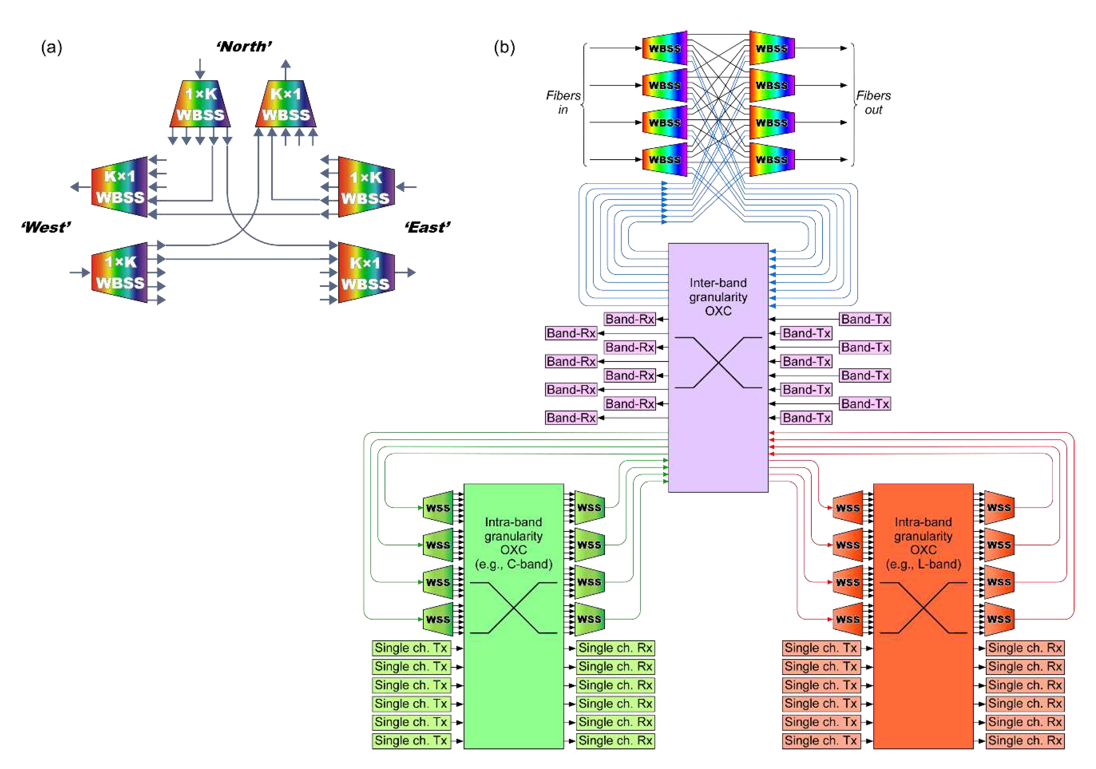
Moreover, even more “exotic” photonic circuits may be implemented over reconfigurable optics, as is the case with waveband selective switches to be discussed in Section 5, to provide processing of optical signal at a very wide bandwidth (over S+C+L amplification bands), routing its spectrum portions in several bands as shown in Figure 15b. Significantly, the reduced waveband count and filter sharpness allow to meet the filtering requirements with multi-tap FIR optical filters, implemented as adaptive lattice filters on a photonic integrated circuit as opposed to bulkier dispersive free-space optics arrangements with LCoS channel selection. Moreover, the design of direct FIR filters (digital and their optical brethren) based on MZI structures alike the TBU is well understood and known to require more stages than IIR filters [58]. Due to the large FSR requirement of the implemented filters (~140 nm), IIR filters of low loss would be hard to implement. The spectral resolution (i.e., the transition bandwidth) of an FIR filter would scale with the FSR divided by the number of taps, such that an implementation comprising a large number of taps (e.g. ≥32) be able to attain improved performance. The cascade of FIR filters, as illustrated in Figure 15c, longitudinally increases the chip size, which in essence is a single input-multiple output interferometer, albeit delivering a better quality spectral response (as shown in Figure 15c). It is worth mentioning that such PIC also requires integrating a large count (~100) of fast phase modulators, to adapt the filter taps and allow for reconfiguration and for better control of the filter response, as it is the case with other Reconfigurable PICs. The basic building block will consist of the tunable band drop filter, implemented by photonic FIR filters. As discussed above, the design of reconfigurable FIR filters has already been demonstrated in [59].
In our opinion, reconfigurable photonic circuits may be both the enabling technology for visionary photonic architectures yet to be realized, as well as providing an immense boost for the all-optical processing needed for optical communications. Finally, several other research fields lacking the know-how of photonic integration and design, and we believe that will benefit from the capabilities of reconfigurable photonic technologies.

4. Optical transmission: key challenges and proposed directions

4.1. Capacity scaling: what to expect in the F6G
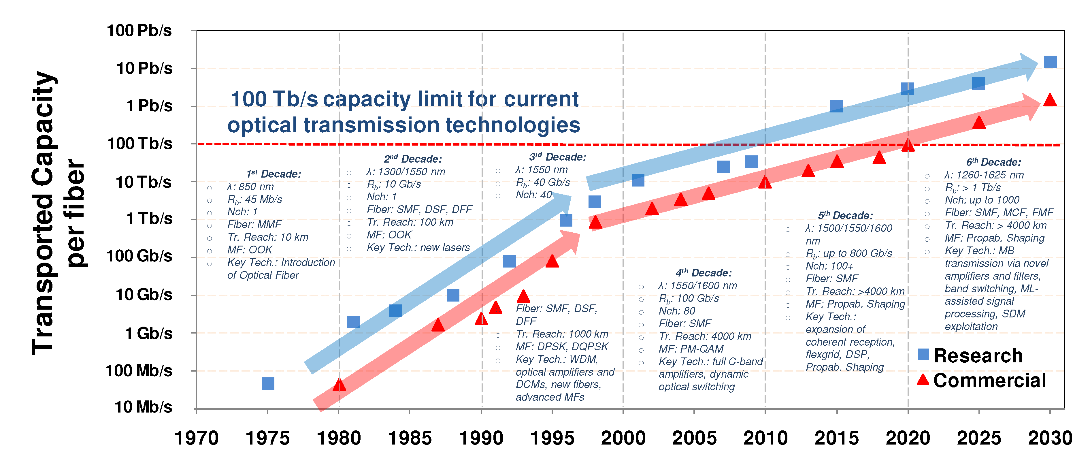
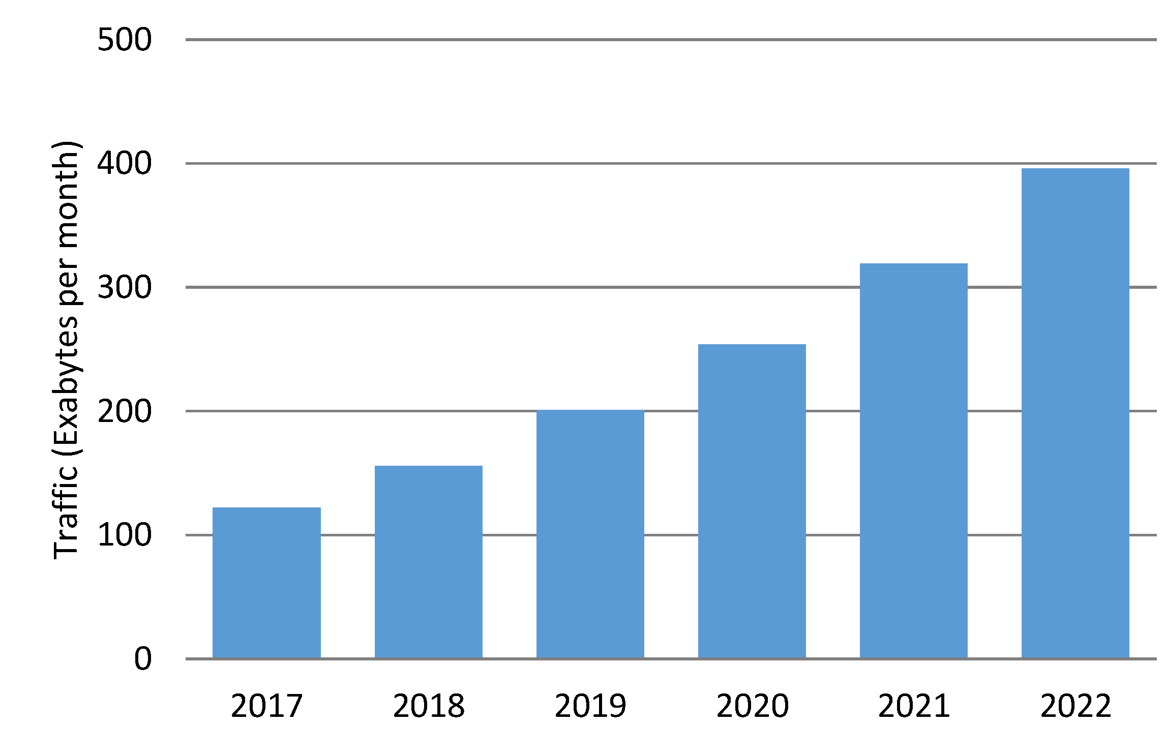
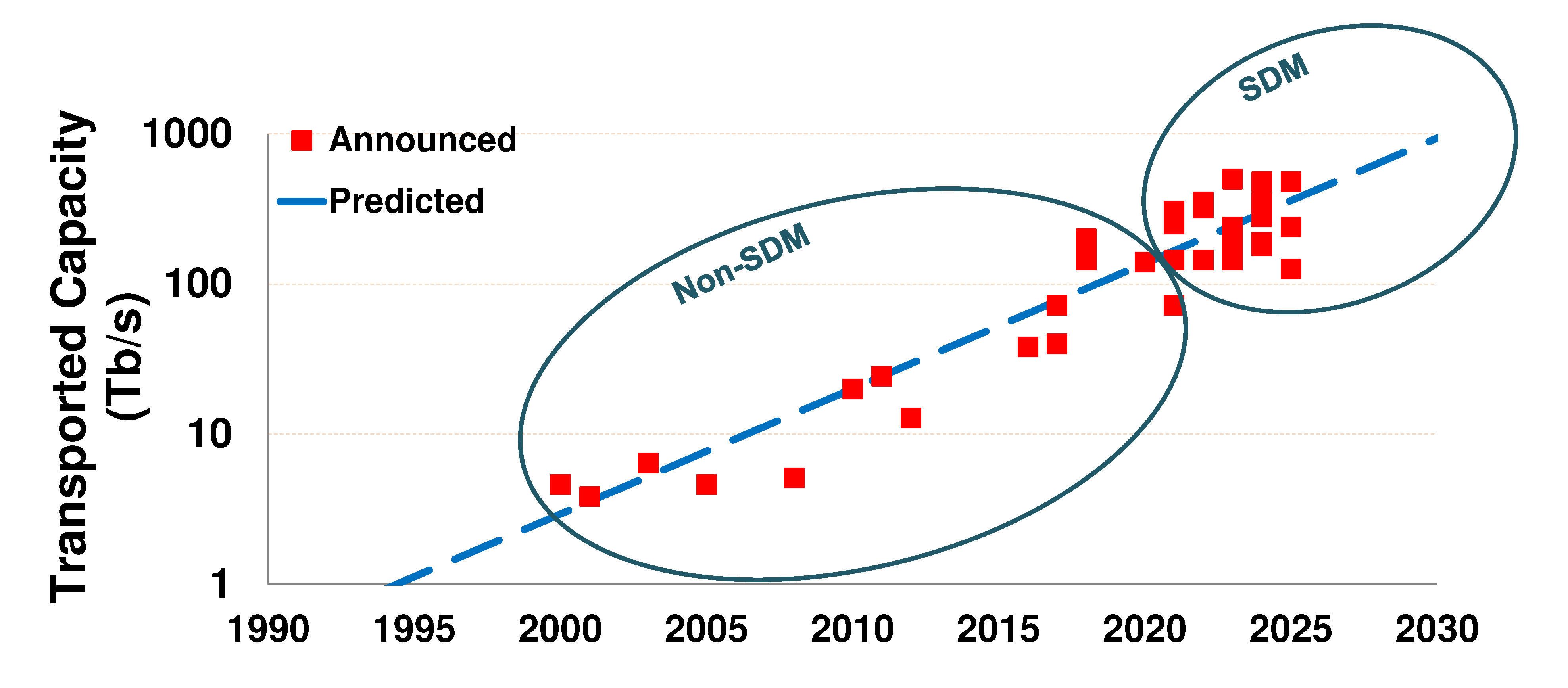
According to Cisco, the traffic demands will keep increasing at a rate of about 100% every 3 years (Figure 16). The reason for this traffic increase, as mentioned in section 2, is the need for meeting the ever-increasing demand for “fresh” services which has been accelerated due to the increased tele-working following the COVID-19 pandemic. So, in order to satisfy the requirements of the upcoming F6G services while at the same time avoiding the 100 Tb/s capacity crunch of the Standard Single Mode Fiber (SSMF), network providers and vendors have to investigate and deploy novel techniques aiming at increasing of at least, one order of magnitude the overall transportation capacity compared with F5G systems. The general trend of transportation capacity per single fiber over time can be seen in Figure 17, according to which during the past five decades, the transportation capacity within an optical fiber started from about some tens of Mb/s and has now reached about 100 Tb/s. This value is the maximum nominal rate of the Single Mode Fiber (SMF) in long-haul transmission. This figure highlights an increase of six orders of magnitude in less than fifty years and clearly underlines the need to find ways in order to exceed 1 Pb/s by 2030.
Recently, various ways have been proposed in order to overcome this 100 Tb/s capacity crunch, such as: a) to exploit more spectrally efficient modulation formats, like probabilistic shaping and coded modulation, b) to exploit the entire low-loss attenuation spectrum of the optical fiber (< 0.4 dB/km) which extends from 1260-1625 nm by transmitting either a higher number of channels or by increasing the bandwidth of each channel (migrating e.g. to higher baud rates) and c) to use SDM, mainly by either considering bundles of SMFs or by using multi-core / mode fibers. In all these three cases, the overall transportation capacity can be extended beyond 100 Tb/s and eventually satisfy the target of 1 Pb/s for 2030 for commercial systems and the target of 10 Pb/s for research works by 2030, as it is illustrated in Figure 17.
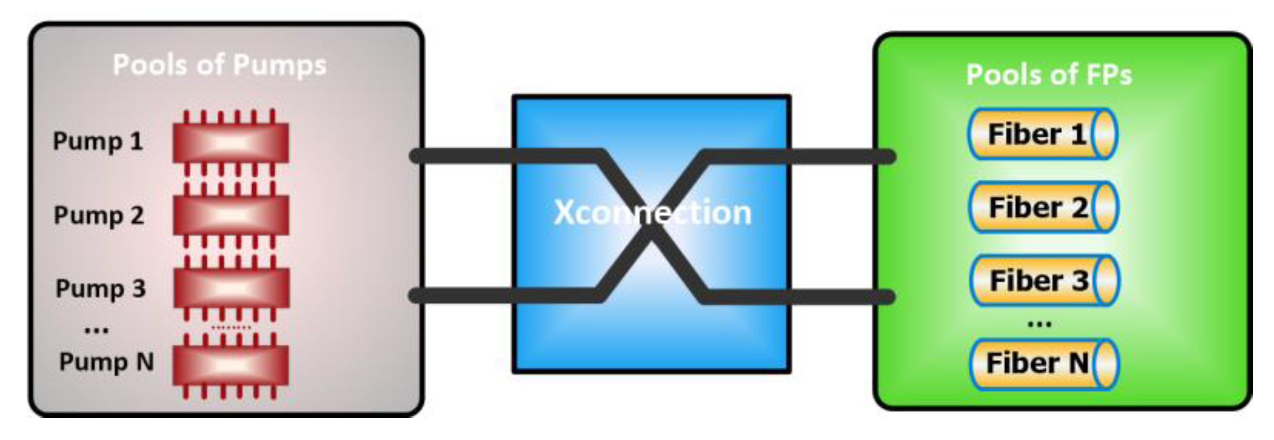
Another observation which can be extracted from this illustration, is that the research technology is about 8-10 years ahead of commercial systems. This is expected, as the results of the huge effort of the researchers around the globe, need to be refined and distilled in order to produce the most cost and at the same time, performance wise methods/technologies/components which will then proceed to commercialization. In order to attain Pb/s rates, novel optical components need to be introduced, such as band filters, cost-efficient optical amplifiers (especially for O and E-bands), band switches and new generation pump sharing SDM based amplifiers which can provide both increased redundancy and reduced costs [60]. Another key technology which can aid the F6G networks to transmit data in even larger distances and/or exploit higher cardinality modulation formats, increasing in this way the transported capacity, is the ML-based signal processing [61]. For example, Deep Neural Networks (DNNs) using digital backpropagation (DBP) methods can achieve a low-complexity nonlinearity compensation. Their performance is similar to those of conventional DBP modules but they encounter relaxed computational complexity.
Figure 17. Evolution of transported capacity within a single mode fiber over the last 50 years along with forecasts for up to 2030 [62,63,64].
Preprints 76390 g017
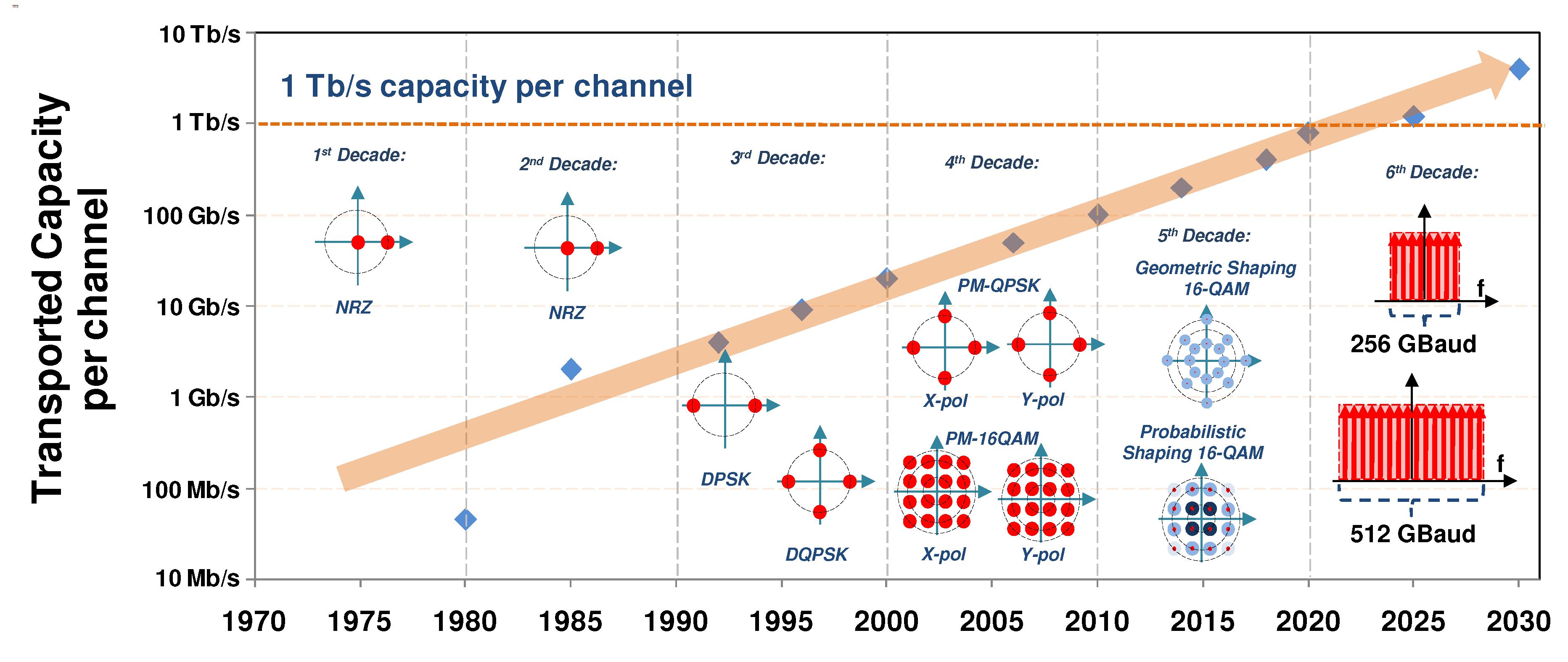
Next, we study the evolution of the capacity per channel over the time interval 1970-2020 in order to understand the general trend and elaborate on the capacity needs for the next decade. Figure 18 highlights the need for fresh commercial systems able to reach at least 2 Tb/s per port by the end of the decade while in [65] the need for up to 6.4 Tb/s by 2031 is also underlined. These rates can be achieved using multiple optical channels packed together forming a super-channel. Today, the highest commercially available rate is 800 Gb/s (Table 4) and can be realized mainly with two options. The first one is to employ a baud rate much larger than those of 100/200G cases, e.g. 90 Gbaud, and the second is to employ more efficient modulation formats, e.g. probabilistic constellation shaping and/or employ a higher cardinality modulation. Each of these alternatives has its own trade-offs, e.g. lower cardinality modulation formats such as 16QAM, require a lower Optical Signal to Noise plus Interference Ratio (OSNIR) in order to attain the same Bit Error Rate (BER) compared with higher cardinality formats, e.g. 64QAM. This, eventually leads to a higher reach for the lower cardinality modulation formats; however, this reach is traded for a higher number of channels, as the lower cardinality formats consume a wider bandwidth for the same data rate. In this case, capacity is traded for connectivity, and the optimal solution is based solely on the high-level design set by the network engineer.
Another observation that can be derived from Table 4 is that the evolution on the baud rate and modulation format from 100G to 800G rates clearly indicates that F6G systems need to adopt transceivers with baud rates of 256 Gbaud and even higher in order to exceed 2 Tb/s. The most recent research works demonstrate baud rates of 168 Gbaud with PM-16QAM format [66] and 220 Gbaud with OOK format [67]. Further, the interplay between attainable reach and bit rate is shown in [68]. In particular, in [68] it is shown that when using 130 Gbaud while considering different modulation formats, rates of 930 Gb/s can be transmitted over 1105 km and rates of 1.28 Tb/s can be transmitted over 452.4 km. Finally, rates of 1.6 Tb/s can be transmitted in a link length of 153.4 km [68]. This analysis clearly designates that in the near future, the technology will show significant progress towards this direction both by stressing the electronics to exceed 512 Gbaud and by using DSPs which will be more tailored to system parameters, than current DSPs, allowing to increase the transmission reach (for longer links). However, for short-reach communication the use of oDAC approaches, as presented in the previous section, seems an excellent approach to scale the data rates in a low cost and low power consumption way.
Figure 18. Evolution of transported capacity per single channel for commercially available systems over the last 50 years along with forecasts for up to 2030 [62,63,64,69,70].
Preprints 76390 g018
Table 4. Details of commercially available transceivers for regional and long-haul transmission [71].
Type Modulation
Format
Baud
Rate
Channel
Spacing
Data
Rate
Required
OSNIR
(for BER=10−3)
100G PM-QPSK 32Gbaud 37.5 GHz 100 Gb/s 9.8 dB
200G PM-16QAM 32Gbaud 37.5 GHz 200 Gb/s 16.55 dB
400G PM-16QAM 63Gbaud 75 GHz 400 Gb/s 16.55 dB
PM-64QAM 42Gbaud 50 GHz 400 Gb/s 22.5 dB
PCS-16QAM 80-95Gbaud 100 GHz 400 Gb/s varies
800G PM-16QAM 128Gbaud 150 GHz 800 Gb/s 16.55 dB
PM-32QAM 96Gbaud 112.5 GHz 800 Gb/s 19.5 dB
PM-64QAM 80Gbaud 100 GHz 800 Gb/s 22.5 dB
PCS-64QAM 90Gbaud 100 GHz 800 Gb/s N/A
200–800G Probabilistic Shaping 60-95Gbaud 75-100 GHz 200-800 Gb/s varies
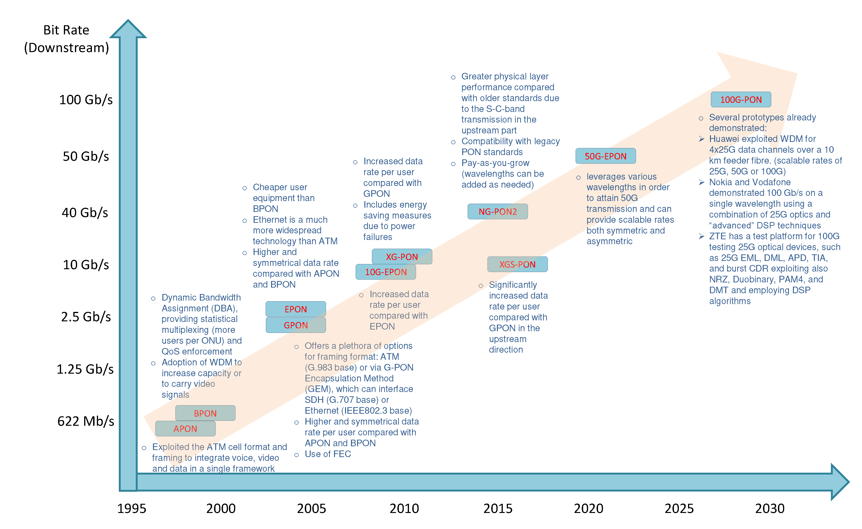
As the rates per channel can reach up to 800 Gb/s with currently available solutions, the attainable rates in the access part of the network are significantly smaller. For example, the most recent PON standard, which is 50G-EPON [72], can provide access to the network with a downstream rate of 50 Gb/s. In the F6G, there is a strong need to advance to an 100G-PON standard or directly to 200G-PON in order to support the various capacity demanding services which were presented in section 2. To further understand this need, Figure 19 illustrates the progress over time of the downstream rate for the various PON standards. Figure 19 also shows the main advantages of each PON standard over its predecessor. These advances on bit rate from standard to standard are a result of the advances on the transceiver operational parameters, such as modulation format, baud rate, operational wavelength and number of wavelengths. It goes with a saying that as the access part of the network is the most cost and power consumption sensitive, direct detection technology stills qualifies to increase the overall rate.
Towards the access rate evolution beyond 50 Gb/s, several options for realizing the 100G-PON have been demonstrated. In the first option, which was presented by Huawei in the BT’s Innovation 2017 exhibition, the system exploited a ValkyrieBay chassis equipped with the unique Xena Loki-100G-5S-1P 5-speed dual-media test module in order to generate Ethernet traffic through the 100G PON. The main purpose of this test was the verification of the overall implementation [73]. More specifically, the system exploited WDM, as four wavelengths were employed to carry 4x25G data channels over a 10 km feeder fiber. This implementation is highly scalable as it can support different rates: 25G, 50G or 100G. The second option, is a 100G PON Prototype developed by ZTE [74] which is an integration test platform featuring many capabilities as it can simulate various modulation formats, like Non-Return-to-Zero (NRZ), Duobinary, PAM4, and DMT (Discrete Multitone) whilst various DSP algorithms can be employed. Moreover, it considers four 25G wavelengths supporting the following four combinations: asymmetric single-wavelength uplink 10G/downlink 25G, symmetric single-wavelength uplink/downlink 25G, asymmetric four-wavelength uplink 40G/downlink 100G, and symmetric four-wavelength uplink/downlink 100G. The feasibility of this prototype was verified at MWC 2017 in Barcelona. The third 100G PON solution was developed by Nokia Bell Labs and validated in Vodafone’s Competence Centre in Eschborn, Germany [75]. This option is based on a single wavelength using a combination of 25G optics and advanced DSP techniques to reach 100 Gb/s. As the 100G PON commercialization is planned for the second half of decade, the next 100G PON standard is expected to be the result of a significant amount of work and conveyed knowledge between the academia, operators, vendors and standardization organizations in order to adopt the most cost and energy efficient solution.
One of the main aspects for the adoption of a PON technology is the maximization of spectral efficiency. Ideal candidates towards achieving this target are Nyquist wavelength division multiplexing PON (Nyquist-WDM-PON) and orthogonal frequency division multiplexing WDM PON (WDM-OFDM-PON). Both solutions can a) provide a finer granularity compared with Time Division Multiplexing (TDM)-PON schemes, b) enable the bandwidth assignment in an as-needed basis and c) maximize spectral efficiency as they have a rectangular spectrum.
In particular, Orthogonal Frequency Division Multiple Access (OFDMA) PON is a well-established technology in wireless and fixed access systems such as WiMAX, long-term evolution (LTE), Asymmetric Digital Subscriber Line (ADSL) and Wi-Fi and can be efficiently incorporated in the PON context to provide significant advantages [76,77,78]. Next, OFDM can be used both for coherent and direct detection schemes. This is important, because when the coherent scheme is adopted, the overall performance can be greatly boosted, and on the other hand, when a DD scheme is considered, low-cost components, such as Directly Modulated Laser (DML), Vertical Cavity Surface Emitting Laser (VCSEL) and low-bandwidth electronics along with DMT can be used, suppressing the overall costs. Finally, OFDMA-PON enables the convergence between wireless and fixed networks allowing to manufacture universal components for both uses.
Further, Nyquist-WDM-PON [79] is a capable solution for PON which aims to minimize the overall number of transceivers, by aggregating multiple transceivers onto a single hub transceiver. The hub transceiver uses coherent technology and multiple combined subcarriers based on Nyquist criterion into a single optical wavelength. In this way, a 100G or a 400G wavelength can be divided into 4 x 25Gb/s or 16 x 25Gb/s subcarriers, respectively or even into a combination of different number of subcarriers and line rates. Using Nyquist-WDM-PON, the network is migrating from point-to-point architecture towards point-to-multipoint, decreasing the overall number of optical interfaces from 2N to N+1, where N is the number of access nodes. This solution provides significant advantages compared with legacy PON systems. The most important are a) decreased number of transceivers due to the use of hub transceivers, b) better routing efficiency, density, and simplicity, as the overall number of ports is significantly decreased, c) better alignment of CapEx with actual bandwidth requirements and quick adaptation on changing bandwidth demands and traffic patterns, d) lower OpEx in terms of power consumption, footprint, number of aggregation sites and support. The concept of Nyquist-WDM-PON has been already commercialized in a version with the name “XR-Optics” [80].
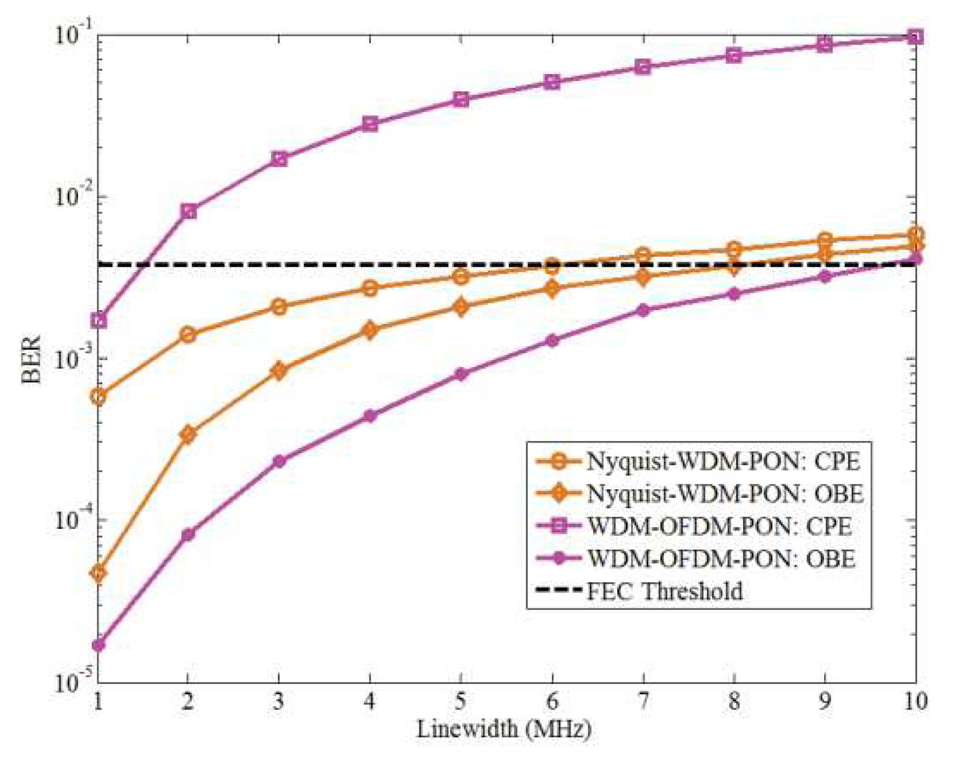
Regarding the physical layer performance of Nyquist-WDM-PON and WDM-OFDM-PON, a comparative analysis is illustrated in [81] and shown in Figure 20. This analysis shows that the physical layer performance is highly dependent on the linewidth, resulting in considerable phase noise. In [81], two phase noise compensation methods were considered, namely, common phase error (CPE) and orthogonal basis expansion (OBE). Nyquist-WDM-PON showed a greater performance compared with WDM-OFDM-PON. This happened as the inter-carrier-interference (ICI) in WDM-OFDM-PON cannot be mitigated by CPE. Next, when OBE is used, WDM-OFDM-PON attains a greater performance than Nyquist-WDM-PON under the two cases, especially at small laser-linewidth. WDM-OFDM-PON is vulnerable to phase noise due to the long OFDM symbol period, but with the aid of effective phase noise suppression method, it can attain a lower BER compared with Nyquist-WDM-PON and eventually qualify as a cost-effective solution for access networks.

4.2. Capacity increase using more spectrally efficient modulation formats

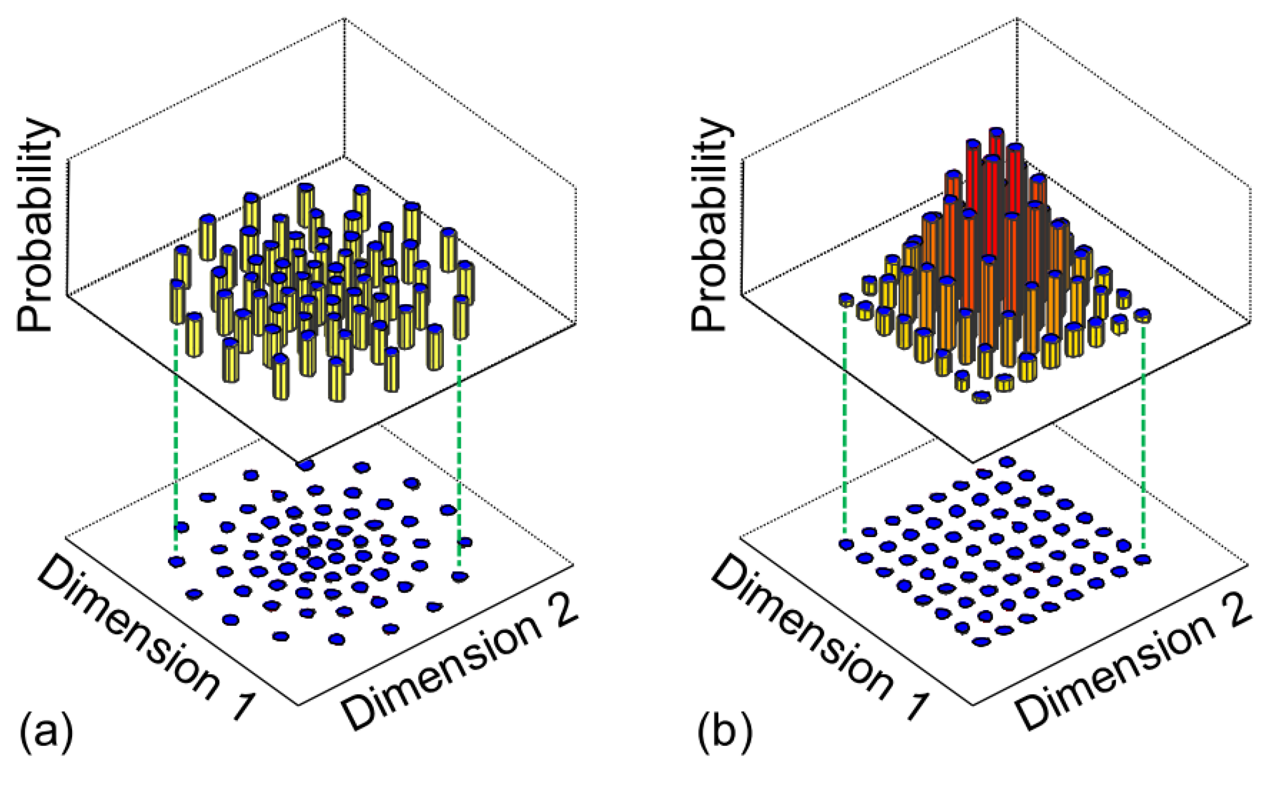
As analyzed above, one option to increase the transportation capacity is to boost the spectral efficiency (SE). SE is a measure of how efficiently the available bandwidth is utilized and equals to the data rate divided by the allocated bandwidth. Higher SE in essence, means that a higher rate can be transmitted using the same spectral width. This can be easily understood, for example, if we consider the 100G and 200G cases of Table 4, where the 200G channels double the data rate by simply tuning the modulation format from QPSK to 16QAM. This increase of the number of “M” states in the M-QAM modulation formats is the most common way to increase the SE in modern coherent optical transmission systems. In addition to this method, there are two other techniques which can aid us exploit the available channel capacity closer to its theoretical limit, which are Probabilistic Constellation Shaping (PCS) and Geometric Constellation Shaping (GCS) [82,83]. These methods deviate from uniform square constellations and can provide important gains in terms of Signal to Noise Ratio (SNR). These two methods are pictorially described in Figure 21.
In GCS, the location of the constellation points in the complex plane is mainly focusing on the areas where the amplitude is small and lesser to the areas where the amplitude is high, optimizing in this way the signal constellation and allowing to approach closer to the fundamental Shannon limit. Two methods for realizing GCS are a) multi-ring constellations, which are used to estimate the Shannon limit of the nonlinear optical fiber channel and b) iterative polar modulation (IPM), which is used to achieve experimental SE records [83]. However, the use of GCS comes with the cost of greater complexity, as more computationally “heavy” DSP modules are required, compared with uniform constellations. A second disadvantage of this method is that there are no simple solutions for finding locations of the GCS constellation points for arbitrary channel conditions and third, the Gray mapping increases the complexity of demapping symbols to soft-decision bit metrics [83].
The second shaping method is the PCS. This method exploits more frequently the inner constellation points that are the less energy/power demanding while the outer points require higher energy and are exploited less frequently. In essence, PCS shapes the probability of occurrence of the constellation points, rather than their locations to approximate Gaussian signaling [83]. This method provides significant gains compared with GCS which are a) it is simple to optimize these probabilities, through a single parameter, to match any given channel condition, b) the constellation points are placed on the rectilinear grid of a square QAM template, which facilitates coherent DSP by robust state of-the-art square-QAM algorithms, and c) Gray mapping facilitates symbol demapping for subsequent SD FEC. Moreover, PCS shows important advantages compared with uniform M-QAM constellations: a) there is a much smaller drop in capacity vs reach relation, allowing for smoother curve, b) the impact of nonlinear effects is reduced, as for the same average power and spectral efficiency, there is a greater Euclidean distance between the constellation points relative to conventional QAM, increasing the overall Optical Signal to Noise Ratio (OSNR), c) it allows to select the baud rate which can guarantee the optimal physical layer performance [84]. It goes with a saying that since PCS is an already commercially deployed technology allowing to reach 800 Gb/s rates, as shown in Table 4, it will keep advancing in order to become one of the key constellation shaping technologies in the F6G long-haul and regional transmission.

4.3. Capacity increase employing a greater number of channels

The second way to increase the transported capacity per fiber is to employ a higher number of channels. For this purpose, two options can be envisaged: a) populate the low loss attenuation spectrum of the single mode fiber (around 365 nm) with channels, extending in this way the transmission beyond the C-band, realizing Ultra-Wideband (UWB) transmission (or named as Multi-Band transmission, however throughout the text we use the term UWB) and/or b) the space dimension can be exploited, e.g. populating a bundle of SMFs, or considering transmission within a Multi Core/Multi Mode/Few Mode Fiber, performing in this way SDM. Both UWB and SDM are candidate approaches for F6G and have their own merits, which will be presented at the rest of this sub-section.

4.3.1. Ultra-Wideband transmission

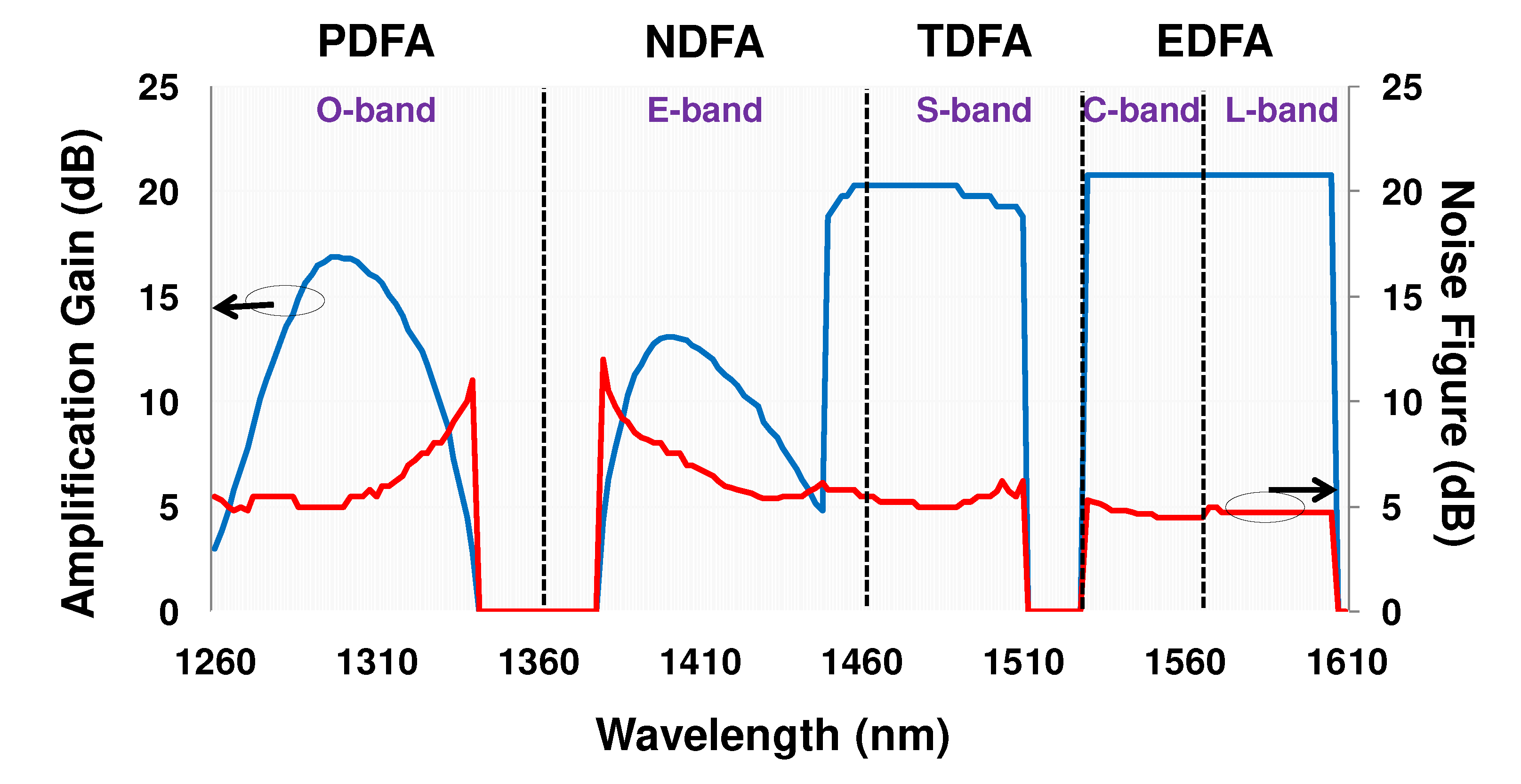
Ultra-Wideband transmission allows for a ten-fold increase in the number of channels compared with the case of C-band transmission only. However, populating the entire low loss attenuation spectrum of the SMF with channels is not trivial, as to-date, optical components such as amplifiers, filters and commercially available transceivers are mainly focused on C and L and parts of S-band. To further understand the current state, Figure 22 illustrates the attainable gain and the noise figure of indicative available doped fiber amplifiers for the five bands of an UWB system. As it can be observed, in O and E-bands, the technology at the component level has to be further developed in order to unlock the transmission of these frequencies. We expect that future research will be able to provide components with the desirable characteristics, such as amplifiers with sufficient gain, with low noise figure and with a significantly wider amplification gain.
To realize UWB transmission, various types of amplifiers can be employed, such as Doped Fiber Amplifiers (DFAs), Semiconductor Optical Amplifiers (SOAs) and Raman amplifiers. The pros and cons of each method are discussed in [71]. According to our opinion, DFAs are currently the dominant amplification technology, as they (a) are a well-known technology due to the extensive use of EDFAs in the C-band, (b) allow for a modular engineering, introducing amplifiers on an as-needed basis, and (c) provide the desirable characteristics such as low noise figure, gain flatness, and high output power. The full potential of an UWB (when all 365 nm are fully exploited) is to transmit more than 1,000 channels (e.g. with 37.5 GHz channel spacing). However, the true number of transmitted channels is expected to be lower, due to the current absence of optical components with the desirable characteristics, especially in O and E-bands as well as the catastrophic impact of nonlinear effects, such as Nonlinear Interference (NLI) and Stimulated Raman Scattering (SRS), the impact of which scales nonlinearly with the increase of the total injected power in the fiber. In particular, [85] showed that by using the currently available technology, the transmission of 871 channels in all five bands can be feasible. However, the attainable capacity of an UWB system depends also on the modulation format “carried” by each channel. For example, if PM-16QAM is considered, an overall rate of 174 Tb/s can be envisaged. Next, the estimation of the transparent reach strongly depends on the impact of the physical layer effects which are a function of various system parameters. In particular, the estimation of transparent reach is a more complex procedure, since each band “sees” different transmission parameters, such as attenuation parameter, local dispersion parameter, effective area etc., and for this reason the attainable reach in each band (even in different channels of the same band) is different, unless an optimization strategy, like [86,87,88], which can ensure similar physical layer performance in all bands is considered.
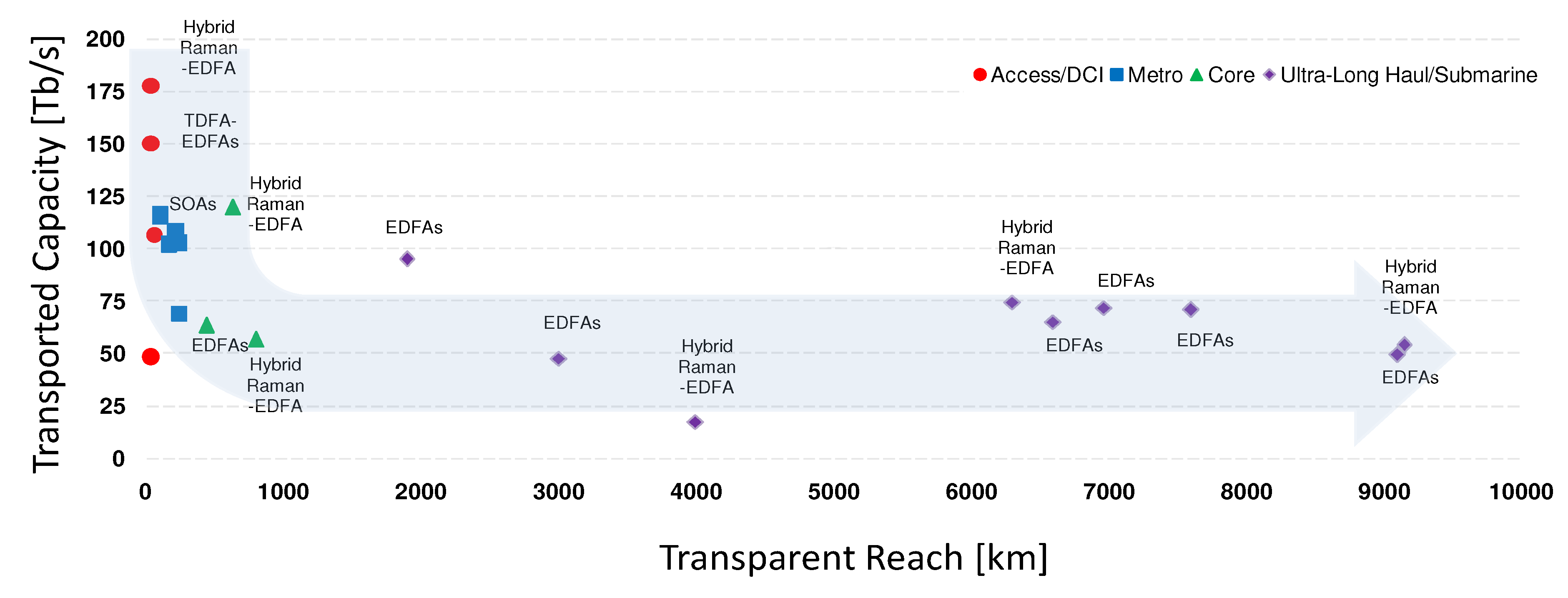
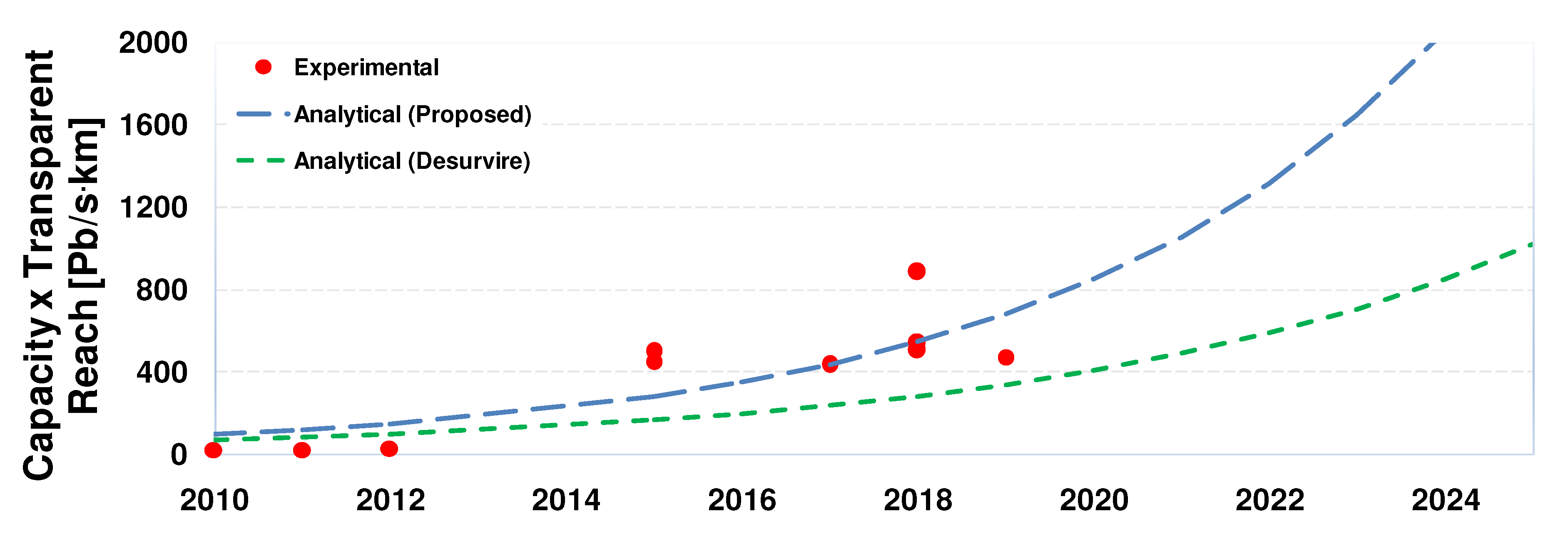
The attainable reach and bit rate are antagonistic target metrics, as when migrating to a higher modulation format, an increased physical layer performance is required in order to attain the same BER. This eventually leads to a lower transparent reach compared with the case of lower cardinality format, e.g. PM-QPSK. This means that rates of > 250 Tb/s can be theoretically achieved in metro, access and inter/intra data center networks while in longer networks, such as submarine and regional, a capacity of up to around 100 Tb/s can be achieved. Figure 23 summarizes the relation between transported capacity and transparent reach up to 10,000 km for experimental works over the past decade [89,90,91,92,93,94,95,96,97,98,99,100,101,102,103,104,105,106,107,108,109,110,111,112,113]. As it is evident from this figure, using either EDFAs alone or in combination with Raman amplifiers, UWB transmission is feasible in long-haul and submarine networks while for shorter distances, e.g. access/DCI and metro, there is a broader gamut of available options for optical amplification. This allows to select the most cost-effective technology between DFAs (e.g. Thulium DFA and EDFAs in parallel), hybrid-Raman amplifiers and SOAs. SOA technology particularly is a very cost-effective option for short distances as it can offer a large amplification bandwidth, e.g. 100 nm with only one amplifier [97,110].
Hollow-core fibers for further increasing the transmission spectrum
The low loss attenuation spectrum of SMF spans over about 50 THz (O to L bands). However, signal transmission beyond this range, in particular from 1800 to 2350 nm, is possible, allowing an about 37 THz additional range using hollow core fibers [64]. In practice, the light in the hollow core fiber propagates within a hollow region, in a way that only a small portion of the optical signal propagates in the solid fiber material. Hollow-core fibers with the proper manufacturing can attain a low fiber loss within a range that spans around 2000 nm. However, the transmission within hollow-core fibers, requires installation of new fibers, which leads to high installation costs and buying prices. This fiber alternative as well as the SDM concept are included in the category of “green-field”, where new fiber types need to be deployed while the UWB transmission are part of the “brown-field” category, where the existing fiber infrastructure is used as the basis for installing new fiber subsystems and elements, such as amplifiers, filters, etc.
An important metric that shows the current state of the technological progress in the optical transmission is the “relative bandwidth”, which equals to the total system bandwidth divided by the central frequency [64]. This metric relates the system bandwidth to its central frequency, and the ultimate target is to approach as close as possible to 100%. For example, a C-band only system shows a relative bandwidth of less than 3%, while a theoretically fully populated UWB system can attain a relative bandwidth of about 25%. Finally, when the transmission spectrum is extended using hollow-core fibers the relative bandwidth can exceed 65%. As the value of this metric increases, the overall system costs are becoming higher, as novel components, such as amplifiers, transceivers, band filters etc. need to be deployed. These components are more costly than those used in C and L-bands, because the technology in C and L-bands bands is more mature and widely adopted, as well as the economy of scale can lead to reduced costs, compared e.g. with E and S-bands. This high cost is a significant constraint for network operators that desire to upgrade their infrastructure towards engaging more bands on optical transmission and can steer them towards exploiting SDM techniques, which are analyzed in the next section.

4.3.2. Space Division Multiplexing

Space Division Multiplexing is in principle a system that incorporates at least one subsystem (e.g. a transmission fiber, an amplifier, a switching node or a terminal equipment) which implements the concept of “spatial integration of network elements”. SDM is of great interest as it promises to increase the overall transported capacity by multiple times compared with one standard SMF. In particular, the main options that can be considered to increase the number of spatial channels within the transmission link are [13]:
  • Multiplication of the number of conventional fibers (thus implementing a parallelism that consists of single-core/single-mode fibers), considering the existence of at least one element that performs spatial integration, e.g. an amplifier with sharing pumps, a switching node, or terminal equipment; named as bundles of Single-Mode Fibers (Bu-SMFs).
  • Multiplication of the number of cores; within the fiber multiple cores arranged within the cladding with each supporting a single spatial mode (Multi-Core Fiber - MCF), or multiple cores each supporting multiple modes (Multi-Core-Mode Fiber - MCMF). Coupled Core (CC) fibers. CC can provide strong mode coupling between the different cores, attaining shorter core-to-core distance and higher spatial density compared with the uncoupled MCFs.
  • Multiplication of the number of modes in MMF fibers; within a single core supporting a discrete number of spatial modes (Multi-Mode Fiber - MMF, Few-Mode Fiber - FMF).
  • A combination of the above categories, e.g. MCF/FMF is also feasible.
  • All these combinations are illustrated in Figure 24.
As mentioned above, in the case of Bu-SMFs, a Bu-SMF to be considered as an SDM, it needs to incorporate at least one sharing scheme, e.g. a pump-sharing scheme in the optical amplifiers/repeaters. It is worth mentioning that the main target of SDM, especially in submarine networks is not to simply increase the number of spatial channels targeting to a higher attainable capacity, but to exploit multiple spatial channels and pump-sharing schemes to achieve a reduction of cost/bit and power/bit quantities, while providing the obvious modular capacity scaling [13].
The comparison between SDM and UWB can designate three main advantages of SDM; the first is its better physical layer performance. In particular, when SDM transmission utilizing the C-band is compared against the lower bands of an UWB system, SDM system benefits from the a) absence of SRS, b) lower attenuation and c) higher dispersion, leading to both decreased ASE and nonlinear effects and eventually to an improved physical layer performance. This not only increases the modulation format cardinality (and so the data rate per channel), but also increases the transparent reach. The latter will lead to a lower number of 3R regenerators in the network (especially in long-haul networks), making SDM systems the ideal candidates for e.g., long-range terrestrial and submarine networks, when compared with UWB. The second advantage of SDM is the use of “spatial integration of network elements”, such as optical amplifiers etc., leading in this way in significantly lower OpEx and CapEx. The third advantage of SDM over UWB is the lower component associated costs, e.g. costs for transceivers, amplifiers and filters.
However, SDM comes with two significant drawbacks. The first is the need to deploy new fibers in links where is an insufficiency of available fibers, however, this is not the case in most links, where abundant dark fibers are present. The second is that SDM cannot attain a diversity on connectivity compared with UWB. More specifically, UWB systems can attain a diversity in connectivity, as the lower bands can employ less costly components employed for shorter links, although these bands result to shorter reach when they are compared with SDM. On the other hand, in UWB, only the C and L-bands can be exploited for the more distant links of a network, which cannot be the case in C-band SDM systems, where the entire available spectrum is considered as “premium” due its high-quality physical layer performance.
Certainly, a combination of SDM/UWB is possible, e.g. by considering a multiple fiber transmission, e.g. Bu-SMFs, exploiting both C and L-bands. However, in order to select the optimal solution between a) the various SDM variants, b) the exploited amplification bands of an UWB system and c) a combination between them, we need to take into account a number of different factors, where many of them are antagonistic, such as attainable capacity, node connectivity, cost/energy-effectiveness, transparent reach, node scalability, system upgradeability and node/spectrum flexibility.
Cost-effectiveness is obviously one of the most important factors when designing an optical network. SDM can reduce the overall component associated costs by exploiting “spatial integration of network elements”, e.g. amplifiers. Considering transmission within multiple modes and/or cores, the most important concern is if these modes/cores intermix. This is an important issue, as a possible energy transfer between them will result in a lower physical layer performance, increasing in this way, the BER of the transmitted channels. For example, in multi-mode fibers, degenerate spatial modes exhibit mixing during fiber propagation while bundles of SMF do not. Proper system design may suppress the impact of this mixing. Further, MCFs’ coupling can be reduced by considering different neighboring core properties and increasing the pitch [114]. Note also, that the placement of identical cores in proximity leads to mutual coupling [115] allowing a more precise control. Mixing between the modes in an MMF can be reduced by breaking the mode group degeneracy [116]. Optical amplification in UWB systems when DFA technology is adopted can be achieved with the use of multiple amplifiers. More specifically, employing a single amplifier for each band, which is placed either in parallel or serial [87]. On the other hand, power feeding in SDM systems utilizing the C-band can be implemented by groups of EDFAs, e.g. one per guided mode, core or fiber [117,118]. A significant benefit of SDM over UWB here is the ability of sharing common pumping lasers [119] reducing in this way the number of laser pumps. SDM is also advantageous when compared with UWB as it possesses the ability to share the lasers in the transmitter and receiver parts [120]. In particular, if mode mixing exists, a common laser source leverages the post-detection signal processing required to unravel the original information, as the phase relationship is fixed. However, SDM shows higher costs than UWB in cases of limited fiber availability or in cases where, due to regulatory aspects, network operators are forced to pay a rent to a government body/agency for any occupied fiber resources. For example, the CAPEX to roll-out a new fiber is ∼25 keuro/km in rural areas, and up to ∼500 keuro/km in metropolitan areas [121]. In particular, for a European country, the lease cost is approximately 0.33x (~ $1308) per fiber/km/year for five years of leasing package; but the lease cost in Indian network is about 0.007x (~ $ 29) per fiber/km/year [122]. These leasing costs need to be quantified during the selection of the optimal solution between UWB and SDM.
The exploitation of SDM in terrestrial networks will not only aid to attain the target of 10 Pb/s by 2030 (Figure 17) but will also significantly boost the node connectivity through the introduction of additional channels which are transmitted through the additional cores and fibers. In particular, the number of parallel cores can reach up to 32 for fiber diameters ≤250 μm, where glass remains flexible, transporting a capacity of 1 Pb/s over more than 200 km [123]. Moreover, with the use of 8D-16QAM format, the transmission distance can exceed 1,200 km with a capacity of 0.75 Pbit/s. Further, in [124] it is demonstrated that the efficient operation of an SDM network is feasible, as the channels are adaptively (re)configured, taking into account the inter-core crosstalk with the aid of a software-defined network (SDN) controller. Towards the introduction of SDM in terrestrial networks, the availability of multi-/core/fiber/mode amplifiers is a prerequisite. In particular, a Multi-Core Erbium/Ytterbium-Doped Fiber Amplifier (MC-EYDFA) can be a promising solution for the power restoration of the channels in multiple cores, however, some challenges need to be addressed, such as the reduction of its size and power consumption. Authors in [125] showed that a 32-core EYDFA can reduce the overall power consumption when benchmarked against a multiple EDFA scheme. This efficiency improvement for cladding pumping originates from increasing the effective area of active cores. Authors in [126] showed increased cladding pump efficiency for 19-core EDFA in C or L-band while a cost-analysis designates that the common amplifier brings long-term cost savings of 33% and up to 55% power savings [127]. In order to realize SDM within the limits of a terrestrial network, the existence of Optical Cross Connects with SDM capabilities is a prerequisite. Scalability is the most important issue in order to accommodate several types of switching granularity demands and a layered switching architecture is mandated. In future SDM networks, when the capacity per path will exceed several Tb/s, the introduction of spatial Optical Cross Connect (OXC) based architectures [128,129] will be a must. The successful migration from current Wavelength Selective Switches (WSS)-based networks towards layered and scalable SDM switches [130,131] will be a key for the success of SDM based networks.
The era of SDM deployments in submarine networks has already started. The first generation of SDM-based submarine systems has been announced and started its deployment phase since 2020, before any terrestrial SDM network of any kind had been deployed. It is characterized by early technology advancements that implement the concept of “spatial integration of network elements” with optical amplifiers. The spatial integration/sharing of resources, is implemented at the submarine optical amplifiers via the so-called “Repeater Pump Farming” (RPF) technique. RPF consists of a group (named “farm”) of repeaters which are cross connected to each other. Each RPF farm supports a certain group of Fiber Pairs (FPs) and utilizes a group of optical pumps that are shared among groups of FPs [132,133]. A significant advantage of RPFs is that they can continue the pumping of FPs even in the cases that one or more pumps fail, offering a promising solution for network survivability, by assuring redundancy. A schematic of an RPF system is illustrated in Figure 25.
SDM in terrestrial and submarine networks
For the realization of SDM, several networking components do exist, such as WSSs and Reconfigurable Optical Add Drop Multiplexers (ROADMs) compared with UWB, in which WSS and ROADMs that can incorporate O, E or S-bands are not in general commercially available. Usually, a submarine OADM node comprises both a Branch Unit (BU) and a Wavelength Management Unit (Figure 26). Fiber pairs may bypass the node (through the BU) if they are routed directly to other destinations or may enter the node to be switched through the WMU BU to their destination. Although flexibility may lead to higher cable utilizations in the case of a reconfigurable OADM, strict security protocols must run to prevent unwanted or faulty node configurations and possible unauthorized access. A comparative analysis between UWB and SDM for the submarine cables is tabulated in Table 5. As it is evident, the SDM can support a significantly larger number of fiber pairs along with very high-power repeaters to rectify the power of the optical signals, which are expected to be significantly larger in number compared with traditional cables. Moreover, the transmission within SDM cables is restricted in C-band, while PCS can be employed to improve the channel performance.
To further understand the potential of SDM systems in increasing the transportation capacity, Figure 27 illustrates the total capacity of deployed submarine cables with and without the use of SDM. From this figure we can observe the trend to migrate to SDM in order to overcome the 100 Tb/s capacity crunch, showing the potential to reach 1 Pb/s by 2030, satisfying in this way the challenging demands of F6G services as they were presented in section 2.
SDM in wireless fronthaul/backhaul
It should be also emphasized that SDM is also an excellent option to support the ever-increasing demands of traffic in the wireless part of the network by offering enhanced fronthaul/backhaul capabilities, as the antenna cell sites (or remote units) are attached via an optical distribution network (ODN), which can exploit SDM [135] (Figure 28). As a consequence, the deployed infrastructure can concurrently support multiple heterogeneous streams of digital and/or analog radio over fiber (DRoF/AroF, respectively), which can distribute heterogeneous traffic in a coordinated fashion through a converged infrastructure. The Central Office (CO) has the capability to exploit space and spectrum resources in an automated way allowing channel establishment between the CO and the cell sites in a 2D space (WDM+SDM), pairing baseband units (BBU) with remote radio units (RRU). As the access requires cost and energy efficient solutions, it will significantly benefit from SDM, using mainly passive components, such as couplers and AWGs. However, the use of active components, such as WSSs, can be considered if the cost needs to be traded with flexible resource allocation.
SDM in inter/intra data center networks
The intra and inter data center communication can greatly benefit from the exploitation of the spatial dimension. The data rates in these two types of networks are usually low, such as 25 Gb/s and up to 100 Gb/s per fiber exploiting mainly direct detection methods, such as NRZ and PAM-4. However, they can be further boosted up to 220 Gb/s OOK, and 408 Gb/s 8-PAM, as shown in [67], increasing the transported capacity (per channel) when needed. Based on the characteristics of currently deployed intra and inter data center networks, a very large number of parallel single mode fibers (>10,000s) is exploited in order to attain Pb/s rates. As a consequence, SDM is an already adopted solution here, where each fiber is populated with only a limited number of channels, e.g., four or eight, giving the opportunity to increase one or two orders of magnitude the overall transported capacity both through the use of a larger number of channels and through increasing the data rate per channel, e.g. via scaling the baud rate.

4.3.3. Summarizing the benefits of UWB and SDM-based systems

Before we conclude this sub-section, we wish to highlight the need to exploit all available capacity scaling dimensions (polarization, amplitude, phase, number of spectral and spatial channels) and tailor them to specific applications and network domains. On one hand, SDM systems based on bundles of SSMFs are an already adopted solution in submarine networks and in intra-datacenter networks. However, the need for their deployment in terrestrial network segments is yet unclear. SDM has also very good potential to support the capacity and connectivity demands of the fronthaul. On the other hand, UWB (i.e. with mainly C and L-band transmission) systems have been a reality for over a decade now. The main question is if UWB is more economically feasible than e.g., a 3-fiber SDM system that achieves the same capacity. To answer this question, one needs to delineate the most cost-effective solutions between SDM, UWD and their combination, accounting for fiber availability, maturity – both at the component and system level – as well as the target total capacity, capacity per lane/channel, transmission reach and the targeted specifications for cost-power consumption per transmitted bit. Towards this target, a technoeconomic analysis on the basis of a network planning study is missing from the literature and needs to be performed for indicative network types, e.g., submarine, access etc.
Regarding the fiber availability, UWB can reach up to 100% availability, as there is at least one fiber present in all network links. On the other hand, SDM in terrestrial links shows a lower fiber availability as the existence of a bunch of dark fibers is not always guaranteed. Next, SDM is advantageous over UWB, as it exploits a well-known and mature technology for various components, such as transceivers, amplifiers, filters etc. since it focuses on the third transmission window. Moreover, the physical layer performance of Bu-SMF is significantly higher when it is compared with UWB systems (beyond C, L-bands), allowing to attain a higher transmission reach, prohibiting the use of UWB applicability in submarine and long-haul transmission systems, as they require a large number of regenerators, especially for the channels in the lower bands. However, in the core domain, as shown in [85], four out of five bands of an UWB system can interconnect even the most distant nodes of a core network, while O-band can be used to interconnect less distant nodes (e.g. up to 600 km), showing that UWB is a very good candidate for the terrestrial domain. This diversity of UWB systems is highly plausible, as different bands can be assigned to different network paths and/or carry different data rates balancing in this way the cost/transparent reach ratio. Merging the advantages of both worlds, we can say that a combination between UWB and SDM systems seems to be the most efficient solution to maximize the terrestrial network connectivity, allowing to transport a multi-thousand number of channels through each optical link.
Next, both UWB and SDM systems have excellent upgradeability capabilities, as a new band or fiber can be engaged when the already active bands or fibers are reaching an utilization threshold, e.g. 60 or 70%, allowing in this way to follow a pay-as-you-grow policy reducing the first-day capital expenditure. Another important advantage of SDM systems compared with UWB ones is the possibility of using common components for a large number of cores/fibers/modes, reducing in this way the overall costs and power consumption. On the other hand, UWB can exploit amplifiers in multiple bands, such as C+L bands EDFA, UWB SOAs and Raman amplifiers, however these components are confined in two or three bands at most. A comparative study between UWB and bundles of C-band SMFs for their most important qualitative features is tabulated in Table 6.
Concluding this sub-section, we wish to underline that using currently available commercial components, it is possible to use in a complementary way UWB alongside SDM systems based on bundles of SMFs. SDM systems based on new fiber types (e.g. MCFs or FMFs) are expected to be further commercialized in the future, due to the immaturity of the technology, performance limitations and the requirement for new fiber deployments that are very costly compared to their alternative solutions. In addition, UWB systems alone can be readily employed, extending the capacity of already deployed SMFs and providing a short to medium-term cost-effective solution for network operators. However, there is a strong need to migrate to the spatial dimension with a rapid pace as it offers a theoretically unbounded capacity multiplier potential allowing to exceed 1 Pb/s rates and can efficiently underpin the upcoming network transformation in order to support 6G and F6G services.

4.3.4. Combining the benefits of UWB and SDM

In this section, we demonstrate how a multi-PB/s TRx block can be formed using UWB and SDM-based systems along with the use of oDAC as it was described in section 3. The oDAC as a building block (BB) can be aggregated using several forms of multiplexing, namely spectral (WDM), spatial (SDM), polarization and quadrature multiplexing, as depicted in Figure 29. The oDAC will be the key component of the transceivers that will enable the aggregation of higher-capacity lanes, in terms of spectral efficiency. TRx’s incorporating single oDACs may suffice to serve low-to-moderate capacity 6G photonics interconnecting fiber links without additional degradation using DD. To achieve higher data rates for the highest UWB capacity, spectral and/or spatial multiplexing can be applied onto the outputs of an array of unipolar or bipolar PAM oDAC outputs.
With the programmable oDAC, we can have a key building block to spur higher-level flexible multiplexing of lanes, combining UWB WDM and SDM to scale the overall transmission capacity up to Pb/s, as depicted in Figure 29. UWB/SDM optical links are then aggregated from per wavelength BBs of up to 2 Tb/s. The envisioned optical link using compact oDAC arrays would support L spectral lanes and N spatial lanes over a single SDM fibre. Having N ≥ 20 and L ≈ 100 (over the S, C and/or L bands), thus L×N =2000, carrying 128 GBaud optical signals and bringing the raw per-link capacity to > 1Pb/s for DD and > 4 Pb/s for COH links.
The oDAC aggregation methodology enables to port and proliferate, at the 6G TRx level, the full benefits of the underlying oDAC BBs, namely the improved tradeoffs in data-rate vs. power dissipation vs. footprint, and the flexibly reprogrammable capacity from relatively slow rates up to UWB capacity. Thus, an oDAC PIC design is classified as “future-proof” as shown in Figure 30.

4.3.5. Towards the ultimate capacity limits of optical transmission

In this sub-section, we briefly elaborate the main factors which can stress the optical transmission towards its practical capacity limits. In order to achieve this, we need to maximize the following three quantities: a) the bit rate per channel, b) the number of employed channels per spatial element, e.g., fiber/core/mode and c) the number of spatial elements. Given that each channel has a specific bandwidth, the bit rate per channel is maximized by selecting a more spectrally efficient modulation format, e.g., 16 or 32QAM instead of QPSK. However, there is a clear tradeoff between the spectral efficiency and the physical layer performance, as the higher cardinality modulation formats require a significantly larger SNR in order to attain the same BER. This is more clear when the Shannon-Hartley theorem is considered, which calculates the spectral efficiency (Sp.Ef.) in the presence of noise as follows:
S p . E f . = C B = log 2 1 + S N
where C is the channel capacity in Gb/s, B the bandwidth of the channel in GHz and S/N the signal to noise ratio. From Eq.(1), it is clear that a high SNR is required to transmit multiple b/s/Hz, which cannot be attained within, e.g. a core network, via for example PM-32QAM, PM-64QAM or even higher cardinality formats, for long distances more than a few hundreds of kilometers [88], mainly due to the accumulation of ASE noise and fiber nonlinearity. In a core network, PM-QPSK or even PM-16QAM can be exploited to interconnect distant nodes [87], as these modulation formats have relaxed SNR requirements compared with higher cardinality formats, in order to attain the same BER. For sure, the spectral efficiency can be boosted using a) sophisticated DSP modules, which can significantly improve the signal’s performance, however with additional computational complexity and added cost/power consumption and b) using more sophisticated forward error correction codes, but at the cost of an increased number of redundant bits. Next, increasing the number of transmitted channels within the same spatial element, e.g. fiber, will directly result to a Nch multiplier. This can be realized by exploiting the low loss attenuation spectrum of the optical fiber as analyzed in section 3.3.1. The ultimate limit of UWB is the 365 nm spectrum, which is obviously finite and after its exploitation, only the third method can be used, which is the space division multiplexing. This method can pack a very large number of spatial elements, in practice much larger than 24, which is the number of the largest SDM system offering another capacity multiplier, allowing to attain multi-Pb/s rates within a single transmission link. The aforementioned analysis is summarized in Figure 31 where the three methods are combined to maximize the number of transmitted data in an optical system.
Predictions on the attainable capacity
Based on the announced capabilities of submarine cables we can perform predictions about the transported capacity for the coming years based on data taken from the previous decades. For this purpose, Figure 32 illustrates the announced transported capacity of various submarine fiber cables [13] with and without SDM. As it is evident, SDM is the key technology that can assist exceeding the limit of 100 Tb/s and reach 1 Pb/s by 2030. These predictions are fully aligned with the predictions of various research works summarized in Figure 17 where it was also highlighted that the capacity of commercially available systems will reach 1 Pb/s at 2030.
Predictions on the attainable capacity times length product can be also performed using the Optical Moor’s Law (OML) formula introduced in [136] for submarine networks as follows
C B P b / s k m = 10 2 Y e a r 2000 / F
where the parameter Year denotes the year selected to estimate the predicted C.B product and F is a parameter that characterizes how fast in time the C.B product is increasing. In the original work of [136], F equals to 3.75, which means a doubling every 3.75 years or every 45 months. In this work, we exploit this formula and based on recent experimental results for ultra-long haul and/or submarine transmission (taken from Figure 23), we slightly update the value of F. In particular, from Figure 33 we can observe that by setting in Eq.(2) an F value equal to 3.125 the fitting error is smaller. This is translated into a doubling of C.B product about every 37.5 months which designates a faster scaling comparing with the value of F equal to 3.75, which to our opinion can be mainly attributed to the unlocking of new amplification bands, which allowed to increase the transported capacity C.

5. Optical Switching: key challenges and proposed directions

5.1. Need for more sophisticated switches to support the F6G ecosystem

Today’s industrial networks are not capable of handling the requirements of the growing IoT ecosystem which incorporates the communication between machines, robots and sensors, especially in the industrial sector. Low data rates, high latency and limited connectivity are the main characteristics of currently deployed networks, and they have become bottlenecks, as they limit industrial manufacturing quality and efficiency. Therefore, there is an urgent demand to provide more bandwidth, ultra-low latency, and higher connectivity in order to handle industry’s time-sensitive traffic flow for automated manufacturing and industrial practices [10]. To further understand the optical switching that is required for the F6G ecosystem, we summarize some key wanted quantities, as they were stated in previous EU-funded HORIZON-CL4-2021-DIGITAL-EMERGING-01-06 call:
  • Reliable and low latency communication with guaranteed service quality for the digital transformation of industrial processes.
  • Reduced congestion in data communication when a multiplicity of applications competes for simultaneous delivery, thereby causing data loss or a delay in data delivery.
  • Reduced power consumption to some pico-Joule per bit through the broader use of optical networking technologies, interconnects, and integrated optical communication components.
  • Lowered barrier for the uptake of higher performance communication technologies by reducing cost of transmission interfaces to around 50 cents per Gigabit per second.
These requirements are critical for the operation of F6G networks and services and to our opinion, a large amount of research work needs to be performed in order to offer the targeted switching components. The currently available solutions for switching, especially for services of the industrial sector, are almost entirely based on electrical interconnects, using expensive copper cables, and electronic switches for the aggregation of the non-time sensitive traffic and point-to-point links for the time sensitive traffic. In the following paragraph we present the main switching challenges which need to be efficiently addressed in order to satisfy the aforementioned requirements.
One technical challenge for the F6G ecosystem is to provide a unified solution that can meet the stringent latency requirements utilizing a P2MP architecture for both time sensitive and non-time sensitive traffic. A second challenge from an economical point of view is to provide a networking solution which can satisfy the cost and power consumption requirements mentioned above, as the traffic demands are scaling with time and are becoming larger. A third challenge is to create consensus around this solution with other system vendors and I4.0 system operators and be able to enter the very competitive, and somewhat closed, market of the optical communication for industrial networks. Finally, the last challenge is to handle the very high capacity which ends up to an optical node and needs to be switched efficiently at its egress. A schematical illustration of the switching concept which can be developed to interconnect both the “Things” within a factory and between the different factories is shown in Figure 34. In this schematic, two different switches are considered, one which is employed to interconnect the various “things” among the various factory floors (OXC-IF) and another one which can switch the traffic to and from the different interconnected factories (OXC-XC). Of course, depending on the factory characteristics and its dimensions, e.g., number of floors, number of interconnected items, it is possible to consider only a single optical switch per factory unit.
In general, the optical switches can be categorized based on their supported services, as defined in section 2, into a) ultra-fast, which are dedicated to Time Sensitive Networks (TSN) and to b) ultra-high capacity, which are dedicated to use-cases that require to switch very high-volume traffic. In the next sub-sections, we discuss the challenges and potential solutions for these two discrete cases, separately.

5.2. Ultra-high capacity switching

To further understand the current needs for ultra-high-capacity switching, we pictorially describe the evolution of switching over time in Figure 35. As it is evident, in the early years (before 2000), it was the Synchronous Digital Hierarchy Digital Cross-Connect (SDH DXC) architecture that was first used to switch SDH-based signals. Electronic switches (SDH DXC) were mainly used in backbone networks operating with WDM technology. During these years, the network topology was entirely fixed with preassigned wavelengths being dropped/added at certain sites with the assistance of OADMs (optical add/drop multiplexers). Later on, OADMs were replaced by ROADMs that brought a level of flexibility and adaptability to the network, as a response to changing needs. Afterwards, planar lightwave circuit (PLC) based ROADM node architecture was initially used to support Add/Drop of wavelength channels to colored ports (fixed port/wavelength assignment), for delivering traffic from/to local premises. This Add/Drop ROADM part used a thermo-optic switch (TO-SW) which was implemented in an PLC. PLC TO-SWs (made from SiO2, which is a quite stable material) have no moving parts and by so, provided enhanced reliability to the ROADM architecture. Another approach comprising the same architecture is the wavelength blocker (WB)-based ROADM node architecture. In this method, the Add/Drop traffic is switched using liquid crystal or micro electromechanical system (MEMS). This approach has good filtering characteristics, yet the dropped (and through) wavelength channels remain wavelength multiplexed. However, the filtering spectrum is broader and sharper than that of an PLC-based ROADM which is based on wavelength demultiplexing.
The Add/Drop switching part (in a WSS-based ROADM) is implemented using MEMS, a liquid crystal or a liquid crystal on silicon (LCOS). Advanced filtering (as in WB-based ROADM), and an excellent multi-degree capability (using multi-port WSSs) are now feasible. The size and complexity of WSS scale with the number of addressable spectral points (= operating bandwidth / optical resolution) and the number of output fiber ports. Increases in these factors lead to more capable ROADMs but with larger and more expensive WSSs. So, we will probably need new optical node switching architectures to support the upcoming UWB/SDM switching.
A few years later, the flex grid concept was introduced as a revolutionary technology that allowed network and service providers to maximize the capacity of their premises by tailoring the channel bandwidth according to user demands. Flex grid is a flexible solution that can support channel spacing from 50 to 200 GHz. A key feature of flex grid is its software configurability. This means that the channel spacing can be dynamically tuned according to specific user demands, offering 6.25 GHz or 12.5 GHz granularity.
Figure 36 depicts a proposed next generation optical switching node architecture which can cross-connect communication channels among spatially parallel links that support UWB/WDM transmission (covering e.g., at first the three distinct bands: S, C, L) and can serve as a part of a Multi-Granular (MG) switch. This architecture will be able to switch traffic from single channels, super-channels, bands, and entire fibers. Therefore, it will be a promising candidate for the future optical switching era.
The switch is usually placed on intermediate nodes (OADMs/ROADMs) in a backbone optical network in order to switch traffic from/to the node. At first, the introduction of WDM in optical transmission required switches with wavelength switching capability. Nowadays, the optical switches have super-channel switching capabilities in order to provide the required traffic from/to different nodes using super-channels, which can provide flexible data rates as the exploited bandwidth is in multiples of 12.5 GHz or even 6.25 GHz. In the coming decades, SDM is expected to be a strong candidate to increase capacity and connectivity, as it was analyzed in section 4, and as a consequence, the development and introduction of full-fiber switches will be a must. However, there will be a strong need for this switch to be MG in order to provide all capabilities between wavelength switching and full-fiber switching. This switch needs to incorporate both WSSs, which can distinguish every wavelength of each incoming fiber and then switch it to the appropriate output port, and WaveBand Selective Switches (WBSSs) which can switch entire amplification bands to the appropriate output ports. The MG-switch will be able to perform switching at the level of i) wavelength, ii) super-channel, iii) band and iv) fully populated with channels fiber, alongside spatial lane switching of i) independent switched, ii) fractionally-joint switched and iii) joint switched spatial super-channels. The development of an WBSSs is an important intermediate step between current super-channel switches and future full-fiber switches.
Several subsystems and technologies are available to implement such a novel optical switching node, but the “missing-link” is a subsystem that can support flexible reconfigurable switching of Ultra-Wide Wavebands, bridging the gap from today’s super-channel switching to tomorrow’s full-spectrum fiber switching. Also, since F6G network nodes will become denser, plentiful and located in more space-limited sites, the switching technology must move away from bulk optics towards more compact, planar technologies. Therefore, the development of a WBSS in PIC format is a must, being able to complement the vital WSSs of today’s state-of-the-art network architectures (thus providing the “missing-link” to the evolution of optical networks). The general concept of the WBSS is pictorially described in Figure 36.
The need for a WBSS switch is further highlighted by Bell Labs which predicted that by 2040, we may need a 250 spatial channels-based network operating over the full (C+L+S)-bands bandwidth, supporting 66 wavelengths with a possible Symbol Rate of 300 Gbaud and a spectral efficiency of 20 b/s/Hz. This system must realize capacity per spatial channel of 400 Tb/s and a total throughput of 100 Pb/s. In this scenario, UWB and SDM need to be combined to transport such amounts of traffic. However, as both techniques introduce new switching challenges at network nodes, the switching scalability is much greater and operation without blocking and contention needs to be ensured. While the available optical fiber switches can be modified to support wider operating wavelength ranges and larger wavelength channel counts, there is no elegant, cost-effective way to do so. Currently available WSSs can be modified to support multi-band transmission but become physically large and costly [137]. Further, OXCs can support wideband operation, but access to wavelength channels necessitates the introduction of demultiplexers, making this option cumbersome and with a large up-front investment requirement. Moreover, both available WSSs and OXCs utilize slow switching mechanisms based on beam-steering to transit from one state to the other and the induced delays are significant. This makes them less suitable for F6G applications which have very stringent latency requirements and need significantly denser networks compared with F5G ones.
In parallel, continuous progress in optical transceivers by way of greater integration of novel photonics and optoelectronic devices, and advancements in DSP are leading to higher capacity optical interfaces (at desired lower cost/bit and energy/bit metrics). As such, optical channel bandwidths are increasing and concurrently the number of wavelength multiplexed channels over a given spectral window is decreasing. This trend suggests that full band transceivers (having integrated frequency comb sources with dedicated modulators and detectors per spectral line) may become commoditized by decade’s end and optical bandwidth will be resourced by full fiber bandwidth and routed throughout the network using space switches, i.e., OXC. This optical networking scenario lacks the efficiencies associated with resource sharing (of fibers, optical amplifiers, switches, etc.) and flexibility to adapt the optical bandwidth utilization to the per connection capacity needs. Furthermore, the optical fiber infrastructure for full fiber allocation per connection will necessarily be massively fiber-parallel and requires that very large OXC to be deployed at network nodes from the onset to support full connectivity [138].
The proposed novel switching paradigm which can address the aforementioned challenges posed for optical switching is pictorially described in Figure 37. This node is able to cross-connect communication channels among spatially parallel links that support UWB/WDM operation (covering e.g., at first the three distinct bands: S, C, L) and can serve as a part of a MG switch which will be able to switch traffic from single channels, super-channels, bands and entire fibers concurrently.
Fundamentally, there is a strong need for a new WBSS module, such as the one pictorially described in Figure 38, that has the following characteristics: a) it is efficiently implemented in an PIC platform, b) it can be adaptively tuned in wavelength and optical bandwidth, c) it can be scalable to large port counts, and d) can operate at microsecond switching rates. Network nodes utilizing the WBSS can be structured in a route-and-select topology, with individual switches placed on each I/O fibre port and expressing band-spanning fiber traffic towards its ultimate destination. The network node architecture supports legacy traffic by conventional WSS at a hierarchy below the WBSS, offering routing to DWDM traffic channels, before being re-multiplexed to the multi-band network (Figure 38). Connectivity between the network hierarchy elements is implemented by an OXC that further assists in transceiver sharing for handling add/drop channels in a colorless/directionless/contentionless (C/D/C) manner. The node can be reconfigured per accepted request in a centralized fashion, as done in today’s networks which lack significant dynamicity, yet accelerated due to a combination of faster processing power for requests and faster response times of the WBSS. An alternative operation mode of cycling through predetermined time-slotted connectivity patterns can allow direct connections between communicating pairs at target switch epochs, with data buffering at the transmitter, thereby guaranteeing time-of-flight latencies across the network and no loss of information due to buffer overflows.

5.2.1. On the road towards realizing a WBSS

Our vision towards this direction for the not-too-distant future networks is based on switches routing entire communication bands (S, C, or L). Multi-band transmission alone will not provide sufficient capacity and links will incorporate SDM solutions as well, as already mentioned in the previous section. Under this upcoming scenario, a new switching paradigm allows to switch entire bands and can offer high output port counts. A new switching architecture needs to be designed and implemented on chip, that combines adaptive filtering for band selection and adaptation as well as crossbar switches for scalable output port counts. The switch needs to be implemented on an PIC platform, on account of its low losses, thermal stability, to utilize fast phase modulators that can operate under 1 μs, to draw very little power per switching event, and be honed to operate with low polarization dependencies.
Moreover, the envisaged hierarchical network node aims to offer fast, route-and-select architecture at the band level implemented at the top tier, with a secondary route-and-select architecture implemented with today’s per band WSS for backwards compatibility with legacy transmission schemes. An OXC disposed in between the two tiers offers C/D/C access to add/drop channels. The network node can be assembled and chassis integrated, sharing a common control plane and communication port, with enhancements for faster network reconfiguration times. Performance characterization of mixed optical circuits flowing through the node, some bands rapidly switched at top tier and others flowing through bottom tier (mimicking legacy DWDM traffic), targeting low crosstalk (≤-20dB) and spurious transient strength (≤1 dB) and duration (≤1μs) on quasi-static, bottom tier flows. These are important technical metrics that can enable the seamless operation of F6G services during their entire life-cycle.

5.2.2. Optical node switching architectures

In currently deployed backbone networks, intermediate nodes (OADMs/ ROADMs) have to switch traffic to their successor nodes in an efficient way. A common practice is to use network elements such as WSSs which can distinguish every wavelength of each incoming fiber and then can switch it to the appropriate output port. So, in this way, there are two main approaches: a) the spatial domain and b) the frequency domain. The spatial domain consists of three main switching strategies: Independent Switching (Ind-Sw), Fractional Joint Switching (Fr-J-Sw) and Joint Switching (J-Sw). The Independent Switching (Ind-Sw) strategy uses wavelengths that can be switched independently in a non-blocking way. The Joint Switching (J-Sw) and the Fractional Joint Switching (Fr-J-Sw) strategies switch wavelengths either all together or in small groups, respectively. However, if the number of fibers and consequently the total number of wavelengths are increased, a ROADM must deploy lots of WSSs, resulting in increased size and cost. On the other hand, the frequency domain consists of WSS, WBSS and finally Full Spectrum Spatial Switching (FSSS). The Wavelength Switching (WS) of uncoupled spatial super-channels approach in [138] switches specific wavelengths of all incoming spatial channels together, an approach similar to J-Sw. The trade-offs are obvious: Ind-Sw strategy switches all data carriers with no limits, but with large sizes and costs. J-Sw, Fr-J-Sw and WS strategies do not provide the high degree of switching freedom (as Ind-Sw does) but can save money and complexity. In the FSSS approach [138], some pre-selected fibers or cores are committed to serve specific source-destination pairs. In FSSS, no wavelength distinction is required in the intermediate nodes, resulting in simpler backbone network architectures. On the other hand, if the traffic demands are much lower than the dedicated fibers’ capacity, the total capacity will be under-utilized. Of course, depending on traffic conditions, hybrid approaches can be deployed.
There has been a lot of scientific research in the above switching architectures so far. A. Neto, et al. in [138] proposed to use Ind-Sw. strategy when dealing with light loads and divert to FSSS when heavy loads arise. This happens because high loads ensure that the capacity of the pre-selected fibers/cores will be fully used. Moreover, authors reviewed several node architectures that can support the Ind-Sw, WS of uncoupled spatial supper-channels and FSSS switching strategies.
As mentioned above, a fundamental element in optical network nodes is the OXC which handles WDM signals without costly optical-to-electrical and electrical-to-optical conversion. It employs integrated interconnections to build an all-optical switching device, achieving high-level integrated, fiber patching-free, and all-optical cross-connections, and manages to improve the switching efficiency especially on large-granularity services.
K. Chen et al. and H. Hasegawa et al. in [139] and [140], respectively, studied the scalability problems of large ROADMs/OXCs due to the rising number of required WSSs. More specifically, authors in [139] proposed a two-level architecture approach to construct a modular large-scale OXC. Several small-scale OXCs are designed and then interconnected to each other in an effort both to ensure full-scale connectivity and reduce the number of devices and intra-node optical links. It is found that this modular OXC design achieves low insertion loss and does not get “big and fat” when input fiber numbers increase.
A proposal of relaxing the full-mesh connectivity to resolve the issue of the large number of required WSSs was presented in [140]. The authors studied the trade-off between full-mesh connectivity and routing performance. They showed that this trade-off can be faced by splitting the inter-connection parts into small regular sub-systems. So, they tried to save space and costs by adding a little more complexity. They finally studied a fiber granular routing as an alternative scheme towards cost-effective switching.
In [141] T. Kuno, et al., experimentally demonstrated a high-throughput OXC architecture that employs spatially-jointed flexible waveband routing. Their results confirmed a net OXC throughput of 2.15 Pb/s, an OXC port count of 84 and a hop count of 7 at the transmission distance of 700 km. Their structure employed 64-channel 400-Gb/s dual-carrier DP-16QAM signals with 75 GHz spacing in 4.8 THz of the full C-band. Finally, authors concluded that this OXC architecture can be applied efficiently to metro networks.
Another way to speed up optical switching is by considering an OXC architecture that deploys spatially jointed flexible-waveband routing using a 37.5 GHz grid, for transmission distance over 1600 km, 700 km, and 600 km using 32 GBaud DP-QPSK, DP-8QAM, and DP-16QAM, respectively. This architecture was presented in [142] and follows a Joint Switching (J-Sw) strategy via deploying special switches (named Delivery and Coupling (DC) switches) which are inserted between J-Sw WSSs for facing possible routing restrictions. Simulations of the proposed architecture showed similar performance with the non-restricted OXC architecture while at the same time complexity and costs were lower. The authors concluded that this architecture could suit to metro networks and will be a cost-effective architecture that could overcome the barriers to the realization of SDM networks.
A very interesting two-layered architecture for ROADMs was presented by J. Zhang et al. in [143]. The two available layers provide a flexible and efficient management of MCF switching and at the same time support traffic grooming and node’s add/drop modules. This two-layer architecture achieved low values in average transmission loss, crosstalk and BER, anticipating the somewhat higher construction complexity. Their findings showed that a multi-layer design can efficiently deal with the scalability issues of single layered ROADMs, and also seems a promising architecture for future ROADMs’ designs.
The last alternative towards higher bandwidth usage is the utilization of extra amplification bands, as analyzed in the previous section. Several recent proposals dictate the concurrent use of S, E and C bands. Theoretically, UWB can use about 50 THz of optical bandwidth from 1260 nm to 1650 nm, thus providing the so wanted extra capacities. The price to be paid will be mainly the greater impact of fiber nonlinear effects in the smaller wavelengths. UWB switching can be built on multiple WSSs and a series of optical amplifiers. So, UWB technology is a promising candidate in an effort to avoid higher sizes and costs and so, to reduce complexity.
N. Fontaine et al. in [144] demonstrated a high port count (47 ports) Ultra-Wideband WSS that can support switching from 1300 nm to 1565 nm with low insertion loss. The switch provides a range of 36 THz (or 250 nm), covers parts of the O band and S, E, C bands.
S. Ding, et al. in [145] proposed a flexibility measurement approach in SDM Elastic Optical Networks (EON) to quantitatively evaluate the switching flexibility of node architectures. Their results showed that an architecture introducing lane changes (LC), employing the Ind-Sw strategy, and maximizing the number of A/D ports and the spectral granularity, can achieve the best switching flexibility performance.
A new OXC structure ([146]) which can effectively reduce the hardware cost by saving the switch scale was presented in [146]. Experimental results showed that the proposed layered m-OXC scheme can achieve similar blocking performance to fully connected OXCs with up to 76.1% hardware scale reduction and 93% searching time reduction.
A new optical network architecture named Spatial Channel Network (SCN) was presented by M. Jinno in [147]. In SCNs, the optical layer “is explicitly decoupled from the hierarchical SDM and WDM layers, and an optical node evolves into a Spatial Cross Connect (SXC) and a Wavelength Cross Connect (WXC) to achieve a Hierarchical Optical Cross Connect (HOXC)”, in an effort to simplify optical switching procedures and protocols.
Moreover, the author presented a Routing and SDM/WDM Multilayer Resource Assignment (RSWA) heuristic protocol in order to minimize the number of needed Spatial Lanes (SLs). An interesting and useful characteristic of SCNs is that they separate traffic demands and network nodes into two kinds. Traffic demands are classified as express and local ones. Express traffic has a SL filling ratio higher than a relatively high threshold. This means that this demand can almost fulfill an SL, and as so, an entire SL is dedicated to it. Although this technique may not use the whole SL’s bandwidth in some cases, it however results to simpler and faster RSWA protocols. Local traffic demands, as they cannot fill an SL, are directed to adjacent specific nodes and multiplexed with other similar traffic. So, SCNs is another way to relax switching demands from the physical layer and thus the needs for large OXCs and move them to an upper layer. In this way, SCNs seem to be able to face the ROADMs’ scalability issues.
We predict that SCNs will be widely used in future optical networks as they combine significantly less hardware in ROADMs (less WSSs) and faster switching for the express traffic class at the small cost of handling two types of traffic and a different (but not necessarily slower) Routing and Wavelength Assignment (RWA) algorithm. We are currently working on deploying the SCNs’ architecture in a recently proposed submarine optical network for the Mediterranean Sea [148] to analytically exploit their potentials.
A recent project that aims to develop optical switches with Multi-band capabilities is the “Flexible Scalable Energy Efficient networking” [149]. FLEX-SCALE has the ambition to develop an UWB+SDM optical node (ON) supporting capacities ≥ 10 Pb/s, facing the scaling challenges and requirements posed by 6G applications on backbone and x-haul networks. This node is based on innovative optical switching technologies such as the novel WBSS and state-of-the-art energy efficient optical transceivers, the oDACs. The main aim of the WBSS is to switch traffic by flexibly defining distinct bands carved from the UWB window of operation (spanning the wavelength range 1460-1625 nm, designated today as the S, C, and L bands) and switching the information-bearing flexible bands (wide spectral super-channels) about ingress-egress fibres using the proven R&S topology. Introducing OXCs and WSS beneath the WBSS, completes the MG-ON, which can then switch communication traffic at full-fibre, flexible-bands, or individual wavelength channel granularity, whilst supporting reconfigurable add-drop in colour-/direction-/contention-less (C/D/C) fashion.
We predict that architectures overcoming the scalability limitations of ROADMs will be more than essential in the near future. A first future direction is the multi-layered OXC architectures (two-layered or even three-layered), as these architectures will need less optical components and fibers, relax the full connectivity OXC demands and provide acceptable fiber/wavelength routing performance. A second direction will be the use of specialized routing and wavelength assignment algorithms, which will meet the upcoming excessive routing/switching needs in the OXCs and at the same time, allow for the use of the more efficient J-Sw strategy. Last, but not least, a third future direction will be the use of both WBSSs and WSSs, preferably within the same node in order to efficiently support Multi-Band switching.

5.3. Ultra-fast switching

Switches that are able to provide very low latency are indispensable components within an Industrial 4.0 and or/a Data Center (DC) environment. In particular, these switches need to
a) offer seamless optical connectivity between factory buildings, micro-data centers or edge cloud computing,
b) ensure low congestion, latency and jitter when routing the traffic flows in the optical domain from the various end-points of the industrial network,
c) provide high scalability and cascadeability, allowing the seamless operation of a highly densified industrial environment, consisting of a large number of inter-connected “things” such as robots, machines etc.,
d) provide a sufficient physical layer performance even for demanding industrial environments, which comprise a large number of inter-connected buildings and “things”, such as robots, machines etc., ensuring a very low BER even after a large number of traversed nodes in a densified environment and
e) provide a cost and energy efficient switching solution which comprises of low cost and zero/low power consumption components (e.g. power splitters, combiners, arrayed waveguide gratings, wavelength blockers).
The switches with these characteristics need to be able to satisfy various Key Performance Indicators (KPIs) concurrently, as the Industrial services are both latency and jitter critical while a high connectivity along with very low packet loss ratio is required. The main KPIs for both intra and inter-factory connectivity are illustrated in Table 7.
Currently available solutions are not able to support TSN as they cannot provide the required levels of flexibility (e.g. traffic dynamics) and determinism (e.g. jitter) concurrently [8]. In particular, Ethernet can effectively support the traffic dynamics however cannot support the required determinism. This is a result of multiple flows which contend for the same output port experiencing random latency, hence jitter. To solve this issue, synchronous arrivals of packets and regular interleaving are needed, which would require client synchronization to the network. Another potential available solution is Industrial Ethernet which provides determinism through its protocols (with sub-µs jitter), however static scheduling hinders their dynamics and flexibility. The next solution according to [8] is Optical Transport Network (OTN), which is deterministic but inflexible. In general, OTN or its variation (FlexE) can meet the current fronthaul requirements, however, they lack of standardization to carry CPRI traffic and limited dynamics, as well as the relative high cost makes them unsuitable for local networks, such as factory floors. Next, the various PON standards can be potential solutions, however they can address either flexibility or determinism but not both at the same time. For example, TWDM-PON through the use of Fixed Bandwidth Assignment (FBA) scheduler can counterbalance jitter, however removing the benefits of statistical multiplexing while reducing the network dynamics, which is static in essence. Finally, the introduction of TSN maintains the trade-off between flexibility and determinism, however it is a very capable solution that offers low-latency, low-jitter, high-speed, and guaranteed delivery use cases [8].
The switching architectures of [7,14] aim to satisfy the requirements of TSN networks. In [7], an optical wavelength, space, and time WDM cross-connect switch is employed to realize the optical metro node architecture and the Data Center Networks (DCN) architecture and consists of express and add/drop ports, photonic integrated WSS aggregation/disaggregation functions for merging/dropping the network traffic, and photonic integrated multi-cast switch (MCS). The modular approach enables to scale the architecture in a pay-as-you-grow approach by using photonic integrated devices for wavelength and space switching. This photonic WDM switch employs SOA as on-chip gain element for lossless operation. A significant advantage of this switch is the fast-switching time of the SOA and the high contrast ratio make the SOA a very good candidate for fast packet-based switching operation. Next, [14], develops a novel DCN architecture utilizing OFDM and parallel signal detection technologies. The candidate architecture offers fine grain bandwidth allocation, high switching speed, and low and uniform latency, which are a must for ultra-fast switches. This implementation has been experimentally demonstrated successfully for the MIMO OFDM switching and fine granularity flexible bandwidth sharing features. Moreover, efficient subcarrier allocation algorithms have been developed for the fine grain bandwidth allocation. The simulation results showed that the MIMO OFDM-based architecture provides low latency and high-throughput switching. Furthermore, the implementation of the scheduler shows that it can support a high number of nodes and subcarriers offering excellent scalability capabilities.
Figure 39 shows the high-level architecture of our vision on the Industry 4.0 switching architecture that aims to support both inter- and intra-factory communication. This architecture aims to connect the variety of end-points that can be found in a modern and future factory environment (including various “things”, such as machines, sensors, robots etc.) with a centralized control that can be seen as micro-data center (microDC), which can be located either within the factory or in a different site. The microDC has the flexibility to host a variety of different services such as the centralized control of the machine and robots on the factory floor, centralized logistic management, digital twin functionalities and predictive maintenance. One of the main advantages of this flexible solution is that services can be migrated seamlessly to micro-DC located in a different location, increasing reliability and availability of the services and allowing for a smooth growth and upgrade of the processing capabilities.
The key element of this network is the Flexible Optical Add/Drop Multiplexing (FOADM) node. This new design will incorporate software-programmable photonic-integrated-circuit based subsystems, controlled by an intelligent software management system, capable of simplifying and optimizing network operations. More specifically, novel photonic switching schemes (optical switches), which are fast-reconfigurable (sub-ms), optimizing the utilization of resources across different kinds of traffic (non/-time-sensitive), using an intelligent control plane, will be implemented. These optical switches allow for fast routing of traffic on individual wavelengths that can be dynamically added, forwarded or dropped at any network point. While the optical switch itself is going to operate at high speed at the order of 10 ns, a key element of this network is going to be the scheduling of the traffic in the FOADM nodes. The scheduling with the assistance of intelligent software management system, will ensure the ultra-low latency and jitter required for traffic delivery in the Industry 4.0 use cases.
In the intra-factory network, the candidate architecture is aiming to provide a solution that will replace the current options for Industrial Ethernet and several other proprietary communications buses. These options are almost entirely based on electrical interconnects, using expensive copper cables, and electronic switches for the aggregation of the non-time sensitive traffic and point-to-point links for the time sensitive traffic. The most advanced demonstration of time sensitive networks over packet switched networks can achieve latency of <100 µs with <100 ns jitter making use of proprietary hardware that essentially creates a point-to-point link through the switches, with a very inefficient use of the network resources [150]. This will aid to develop a solution using a low-cost P2MP fiber network that will replace the copper based electrical interconnects with an optical fiber and passive splitters/combiners. The proposed network aims to support both time sensitive and time insensitive connectivity. While the time insensitive traffic can be easily supported terminating and aggregating the connections from the end points at the input of the optical switch, the time sensitive traffic and connections will be forwarded directly on the network by the FOADM node.
The intra-factory solution can support optical aggregation of up to 64 end-points with data rates up to around 1 Gb/s per end-point and distances of a few kilometers. The solutions will use PON interfaces and technologies developed for residential optical access networks, such as XGS-PON and NG-PON2. In order to interface with the proposed optically switched network and meet the required latency and reliability performances, scheduling of the traffic in the PON systems will need to be integrated with new designs of the overall architecture. The design of the PON scheduler can be based on the work done in utilizing TDM-PON for fronthaul applications [151].
The proposed solution can effectively address all the KPIs of Table 7 set for ultra-fast switches whilst in addition it will allow to: i) reduce the congestion, since optical networks can support high capacity; ii) reduce the power consumption, due to the lower consumption of optical components in comparison with electronic ones, and, iii) reduce the cost of transmission interfaces thanks to the use of end-to-end optics, avoiding intermediate conversions to the electrical domain thus collectively improving performance while at the same time minimizing the environmental impact. The fact that the control can be performed only at the edges of the network, makes the above solution an ideal candidate for F6G ecosystems.

6. Conclusions

The 6th generation of fixed networks is about to offer to humankind new services about to exert profound impact upon all aspects of human activity. In this vision article, we first categorized the key F6G services and shed light on their main requirements, to be met concurrently: low latency, high bit rate and ample connectivity. Next, we examined the main building blocks of the network to be developed using low-cost and low power-consumption techniques. In particular, acknowledging that electronics is approaching its limits, and all-optical techniques will be increasingly called ‘to the rescue’, we explained how our proposed adoption of an optical-DAC is fully aligned with and supports the trend of improved energy-efficiency and enhanced performance. Moreover, we presented three strategies to increase the rate of transmitted data in an optical system: use of more spectrally efficient modulation formats, full exploitation of the physically available amplification bands of SMF and adoption of SDM. The implementations of each of these strategies or a combination thereof, depend on the network domain -e.g., metro vs. core - and on target constraints on cost, footprint and power dissipation. Further, we discussed the two classes of optical switches featuring ultra-fast (enabling Time-Sensitive services) vs. ultra-high capacity (enabling use-cases that require switching very high-volume traffic) along with their requirements. Finally, we proposed potential solutions based on the development of multi-granular waveband-selective flexibly switched optical add/drop multiplexing node, respectively.

Author Contributions

All authors have contributed to the conceptualization, methodology approach development, editing, writing and reviewing of the article. All authors have read and agreed to the published version of the manuscript.

Funding

This research received no external funding.

Data Availability Statement

The data discussed in this article have been referenced at the corresponding points.

Conflicts of Interest

The authors declare no conflict of interest.

References

  1. Wild, T.; Braun, V.; Viswanathan, H. Joint Design of Communication and Sensing for Beyond 5G and 6G Systems. IEEE Access 2021, 9, 30845–30857. [Google Scholar] [CrossRef]
  2. Stavdas, A. 5G as a Catalyst for a Wider Technological Fusion that Enables the Fourth Industrial Revolution. Competitive Advantage in the Digital Economy (CADE 2021). LOCATION OF CONFERENCE, COUNTRYDATE OF CONFERENCE; pp. 39–49.
  3. Stavdas, “Networked Intelligence: A Wider Fusion of Technologies that Spurs the Fourth Industrial Revolution”, World Review of Political Economy, Part I: Foundations, Vo. 12 (2), p.220-235, 2021; Part II: The Transformation of Production Systems, Vo.12 (2), p.236-254, 2021. [Google Scholar]
  4. Uzunidis, D.; Logothetis, M.; Stavdas, A.; Hillerkuss, D.; Tomkos, I. Fifty Years of Fixed Optical Networks Evolution: A Survey of Architectural and Technological Developments in a Layered Approach. Telecom 2022, 3, 619–674. [Google Scholar] [CrossRef]
  5. Fifth Generation Fixed Network (F5G); F5G Generation Definition Release #1.
  6. The Fifth Generation Fixed Network (F5G): Bringing Fiber to Everywhere and Everything”, ETSI White Paper No. #41, September 2020.
  7. Calabretta, N.; Prifti, K.; Tessema, N.; Xue, X.; Pan, B.; Stabile, R. Photonic integrated WDM cross-connects for optical metro and data center networks. Metro and Data Center Optical Networks and Short-Reach Links II. LOCATION OF CONFERENCE, United StatesDATE OF CONFERENCE; p. 1094603.
  8. Pointurier, Y.; Benzaoui, N.; Lautenschlaeger, W.; Dembeck, L. End-to-End Time-Sensitive Optical Networking: Challenges and Solutions. J. Light. Technol. 2019, 37, 1732–1741. [Google Scholar] [CrossRef]
  9. Benzaoui, N.; Gonzalez, M.S.; Estaran, J.M.; Mardoyan, H.; Lautenschlaeger, W.; Gebhard, U.; Dembeck, L.; Bigo, S.; Pointurier, Y. Deterministic Dynamic Networks (DDN). J. Light. Technol. 2019, 37, 3465–3474. [Google Scholar] [CrossRef]
  10. Bigo, S.; Benzaoui, N.; Christodoulopoulos, K.; Miller, R.; Lautenschlaeger, W.; Frick, F. Dynamic Deterministic Digital Infrastructure for Time-Sensitive Applications in Factory Floors. IEEE J. Sel. Top. Quantum Electron. 2021, 27, 1–14. [Google Scholar] [CrossRef]
  11. Richardson, D. J. "New optical fibers for high-capacity optical communications." Philosophical Transactions of the Royal Society A: Mathematical, Physical and Engineering Sciences 374.2062 (2016): 20140441.
  12. Saridis, G.M.; Alexandropoulos, D.; Zervas, G.; Simeonidou, D. Survey and Evaluation of Space Division Multiplexing: From Technologies to Optical Networks. IEEE Commun. Surv. Tutorials 2015, 17, 2136–2156. [Google Scholar] [CrossRef]
  13. Papapavlou, C.; Paximadis, K.; Uzunidis, D.; Tomkos, I. Toward SDM-Based Submarine Optical Networks: A Review of Their Evolution and Upcoming Trends. Telecom 2022, 3, 234–280. [Google Scholar] [CrossRef]
  14. Ji, P.N.; Qian, D.; Kanonakis, K.; Kachris, C.; Tomkos, I. Design and Evaluation of a Flexible-Bandwidth OFDM-Based Intra-Data Center Interconnect. IEEE J. Sel. Top. Quantum Electron. 2012, 19, 3700310–3700310. [Google Scholar] [CrossRef]
  15. Marom, D.M.; Colbourne, P.D.; D’Errico, A.; Fontaine, N.K.; Ikuma, Y.; Proietti, R.; Zong, L.; Rivas-Moscoso, J.M.; Tomkos, I. Survey of Photonic Switching Architectures and Technologies in Support of Spatially and Spectrally Flexible Optical Networking [Invited]. J. Opt. Commun. Netw. 2017, 9, 1–26. [Google Scholar] [CrossRef]
  16. Rechtman, L.; Marom, D.M. Rectangular versus circular fiber core designs: New opportunities for mode division multiplexing?. Optical Fiber Communication Conference. LOCATION OF CONFERENCE, United StatesDATE OF CONFERENCE; p. Th2A.10.
  17. Jinno, M. Spatial Channel Network (SCN): Opportunities and Challenges of Introducing Spatial Bypass Toward the Massive SDM Era [Invited]. J. Opt. Commun. Netw. 2019, 11, 1–14. [Google Scholar] [CrossRef]
  18. N. Jones, “The information factories”, in Nature, vol 561, September 2018. 20 September.
  19. Nazarathy, M.; Tomkos, I. Accurate Power-Efficient Format-Scalable Multi-Parallel Optical Digital-to-Analogue Conversion. Photonics 2021, 8, 38. [Google Scholar] [CrossRef]
  20. Yariv, A. Dynamic analysis of the semiconductor laser as a current-controlled oscillator in the optical phased-lock loop: applications. Opt. Lett. 2005, 30, 2191–2193. [Google Scholar] [CrossRef]
  21. Chen Xi et al., “Kramers-Kronig receivers for 100-km datacenter interconnects,” Journal of Lightwave Technology, vol. 36, no. 1, pp. 79-89, 2018.
  22. Nazarathy, M.; Agmon, A. Doubling direct-detection data rate by polarization multiplexing of 16-QAM without active polarization control. Opt. Express 2013, 21, 31998–32012. [Google Scholar] [CrossRef]
  23. Tomkos, I.; Tolmachev, A.; Agmon, A.; Meltsin, M.; Nikas, T.; Nazarathy, M. Low-Cost/Power Coherent Transceivers for Intra-Datacenter Interconnections and 5G Fronthaul Links. 2019 21st International Conference on Transparent Optical Networks (ICTON). LOCATION OF CONFERENCE, FranceDATE OF CONFERENCE; pp. 1–5.
  24. Morsy-Osman, M.; Sowailem, M.; El-Fiky, E.; Goodwill, T.; Hoang, T.; Lessard, S.; Plant, D.V. DSP-free ‘coherent-lite’ transceiver for next generation single wavelength optical intra-datacenter interconnects. Opt. Express 2018, 26, 8890–8903. [Google Scholar] [CrossRef]
  25. Doerr, C.R.; Chen, L. Monolithic PDM-DQPSK receiver in silicon. 2010 36th European Conference and Exhibition on Optical Communication - (ECOC 2010). LOCATION OF CONFERENCE, ItalyDATE OF CONFERENCE; pp. 1–3.
  26. Perin, J.K.; Shastri, A.; Kahn, J.M. Design of Low-Power DSP-Free Coherent Receivers for Data Center Links. J. Light. Technol. 2017, 35, 4650–4662. [Google Scholar] [CrossRef]
  27. M. S. Erkılınc¸, D. M. S. Erkılınc¸, D. Lavery, B. C. Thomsen, R. I. Killey, P. Bayvel, and S. J. Savory, “Polarization-insensitive single-balanced photodiode coherent receiver for long-reach WDM-PONs,” J. Lightw. Technol., vol. 34, no. 8, pp. 2034–2041, Apr. 2016.
  28. Cano, I.N.; Lerin, A.; Polo, V.; Prat, J. Polarization independent single-PD coherent ONU receiver with centralized scrambling in udWDM-PONs. 2014 European Conference on Optical Communication (ECOC). LOCATION OF CONFERENCE, FranceDATE OF CONFERENCE; pp. 1–3.
  29. Kazovsky, L.; Meissner, P.; Patzak, E. ASK multiport optical homodyne receivers. J. Light. Technol. 1987, 5, 770–791. [Google Scholar] [CrossRef]
  30. Zhou, J.; Caponio, N. Operative characteristics and application aspects of synchronous intra-bit polarization spreading for polarization independent heterodyne detection. IEEE Photon- Technol. Lett. 1994, 6, 295–298. [Google Scholar] [CrossRef]
  31. Ciaramella, E. Polarization-Independent Receivers for Low-Cost Coherent OOK Systems. IEEE Photon- Technol. Lett. 2014, 26, 548–551. [Google Scholar] [CrossRef]
  32. Altabas, J. A., Silva Valdecasa, G., Didriksen, M., Lazaro, J. A., Garces, I., Tafur Monroy, I., & Jensen, J. B. (2018). Real-time 10Gbps Polarization Independent Quasicoherent Receiver for NG-PON2 Access Networks. In Proceedings of 2018 Optical Fiber Communications Conference and Exposition: OFC 2018 (pp. 1-3).
  33. Thomas, V.A.; Varughese, S.; Ralph, S.E. Quasicoherent Receivers for Access Networks Using Fullwave Rectification Based Envelope Detection. CLEO: Science and Innovations. LOCATION OF CONFERENCE, United StatesDATE OF CONFERENCE; p. SM4G.4.
  34. B. Murmann, “ADC Performance Survey 1997-2021,” [Online]. Available: http://web.stanford.edu/~murmann/adcsurvey.html.
  35. Siegman, A.; Kuizenga, D. Proposed method for measuring picosecond pulsewidths and pulse shapes in CW mode-locked lasers. IEEE J. Quantum Electron. 1970, 6, 212–215. [Google Scholar] [CrossRef]
  36. G. C. Valley, “Photonic analog-to-digital converters,” Opt. Express 15(5), 1955–1982 (2007).
  37. Khilo, A.; Spector, S.J.; Grein, M.E.; Nejadmalayeri, A.H.; Holzwarth, C.W.; Sander, M.Y.; Dahlem, M.S.; Peng, M.Y.; Geis, M.W.; DiLello, N.A.; et al. Photonic ADC: overcoming the bottleneck of electronic jitter. Opt. Express 2012, 20, 4454–4469. [Google Scholar] [CrossRef] [PubMed]
  38. Yariv, A.; Koumans, R. Time interleaved optical sampling for ultra-high speed A/D conversion. Electron. Lett. 1998, 34, 2012–2013. [Google Scholar] [CrossRef]
  39. B. Krueger et al., “A monolithically integrated, optically clocked 10 GS/s sampler with a bandwidth of >30 GHz and a jitter of <30 fs in photonic SiGe BiCMOS technology,” in Proc. IEEE Custom Integrated Circuits Conference (CICC), 2017.
  40. Taylor, H.F.; Taylor, M.J.; Bauer, P.W. Electro-optic analog-to-digital conversion using channel waveguide modulators. Appl. Phys. Lett. 1978, 32, 559–561. [Google Scholar] [CrossRef]
  41. Nazarathy, M.; Shaham, O. Spatially distributed successive approximation register (SDSAR) photonic ADCs based on phase-domain quantization. Opt. Express 2012, 20, 7833–7869. [Google Scholar] [CrossRef]
  42. Lopez, I.G.; Aimone, A.; Alreesh, S.; Rito, P.; Brast, T.; Hohns, V.; Fiol, G.; Gruner, M.; Fischer, J.K.; Honecker, J.; et al. DAC-Free Ultralow-Power Dual-Polarization 64-QAM Transmission at 32 GBd With Hybrid InP IQ SEMZM and BiCMOS Drivers Module. J. Light. Technol. 2016, 35, 404–410. [Google Scholar] [CrossRef]
  43. Schell, M.; Fiol, G.; Aimone, A. DAC-free Generation of M-QAM Signals with InP Segmented Mach-Zehnder Modulators. In Proceedings of the 2017 Optical Fiber Communications Conference and Exhibition OFC, Los Angeles, CA, USA, 19–23 March 2017. [Google Scholar]
  44. Patel, D.; Samani, A.; Veerasubramanian, V.; Ghosh, S.; Plant, D.V. Silicon Photonic Segmented Modulator-Based Electro-Optic DAC for 100 Gb/s PAM-4 Generation. IEEE Photon- Technol. Lett. 2015, 27, 2433–2436. [Google Scholar] [CrossRef]
  45. Sobu, Y.; Huang, G.; Tanaka, S.; Tanaka, Y.; Akiyama, Y.; Hoshida, T. High-Speed Optical Digital-to-Analog Converter Operation of Compact Two-Segment All-Silicon Mach–Zehnder Modulator. J. Light. Technol. 2020, 39, 1148–1154. [Google Scholar] [CrossRef]
  46. Vanhoecke, M.; Argyris, N.; Aimone, A.; Dris, S.; Apostolopoulos, D.; Verheyen, K.; Vaernewyck, R.; Torfs, G.; Yin, X.; Bosman, E.; et al. Multi-level optical signal generation using a segmented-electrode InP IQ-MZM with integrated CMOS binary drivers. In Proceedings of the 42nd European Conference on Optical Communication, ECOC, Dusseldorf, Germany, 18–22 September 2016; pp. 352–354. [Google Scholar]
  47. Aimone, A.; et al. In Proceedings of the 2016 Optical Fiber Communications Conference and Exhibition, OFC 2016, Anaheim, CA, USA, 20–24 March 2016; Volume 1, pp. 15–17. [Google Scholar]
  48. Aimone, A.; Frey, F.; Elschner, R.; Lopez, I.G.; Fiol, G.; Rito, P.; Gruner, M.; Ulusoy, A.C.; Kissinger, D.; Fischer, J.K.; et al. DAC-Less 32-GBd PDM-256-QAM Using Low-Power InP IQ Segmented MZM. IEEE Photon- Technol. Lett. 2016, 29, 221–223. [Google Scholar] [CrossRef]
  49. Ehrlichman, Y.; Amrani, O.; Ruschin, S. Improved Digital-to-Analog Conversion Using Multi-Electrode Mach–Zehnder Interfer- ometer. J. Light. Technol. 2008, 26, 3567–3575. [Google Scholar] [CrossRef]
  50. Giuglea, A.; Belfiore, G.; Khafaji, M.; Henker, R.; Petousi, D.; Winzer, G.; Zimmermann, L.; Ellinger, F. Comparison of Segmented and Traveling-Wave Electro-Optical Transmitters Based on Silicon Photonics Mach-Zehnder Modulators. 2018 Photonics in Switching and Computing (PSC). LOCATION OF CONFERENCE, CyprusDATE OF CONFERENCE; pp. 1–3.
  51. Verbist, J.; Verplaetse, M.; Lambrecht, J.; Srivinasan, S.A.; De Heyn, P.; De Keulenaer, T.; Pierco, R.; Vyncke, A.; Absil, P.; Yin, X.; et al. 100 Gb/s DAC-less and DSP-free Transmitters using GeSi EAMs for Short-Reach Optical Interconnects. Optical Fiber Communication Conference. LOCATION OF CONFERENCE, United StatesDATE OF CONFERENCE; p. W4D.4.
  52. Yamazaki, H.; Yamada, T.; Goh, T.; Mino, S. Multilevel Optical Modulator with PLC and LiNbO3 Hybrid Integrated Circuit. Optical Fiber Communication Conference. LOCATION OF CONFERENCE, United StatesDATE OF CONFERENCE; p. OWV1.
  53. Sano, A.; Kobayashi, T.; Ishihara, K.; Masuda, H.; Yamamoto, S.; Mori, K.; Yamazaki, E.; Yoshida, E.; Miyamoto, Y.; Yamada, T.; et al. 240-Gb/s polarization-multiplexed 64-QAM modulation and blind detection using PLC-LN hybrid integrated modulator and digital coherent receiver. In Proceedings of the European Conference on Optical Communication, Vienna, Austria, No. 1, 20–24 September 2009;-Suppl; Volume 2009, p. 2. [Google Scholar]
  54. Yamazaki, H.; Yamada, T.; Goh, T.; Kaneko, A. PDM-QPSK Modulator With a Hybrid Configuration of Silica PLCs and LiNbO$_{3}$ Phase Modulators. J. Light. Technol. 2010, 29, 721–727. [Google Scholar] [CrossRef]
  55. Yamazaki, H.; Yamada, T.; Goh, T.; Kaneko, A. 64QAM Modulator with a Hybrid Configuration of Silica PLCs and LiNbO3 Phase Modulators for 100-Gb/s Applications Hiroshi. In Proceedings of the ECOC 2009, Vienna, Austria, 20–24 September 2009; paper 2.2.1. [Google Scholar]
  56. Nazarathy, M.; Tomkos, I. Energy-Efficient Reconfigurable 4|16|64|256-QAM Transmitter Based on PAM2|4-Driven Optical DACs. IEEE Photon- Technol. Lett. 2022, 34, 1159–1162. [Google Scholar] [CrossRef]
  57. Bogaerts, W.; Pérez, D.; Capmany, J.; Miller, D.A.B.; Poon, J.; Englund, D.; Morichetti, F.; Melloni, A. Programmable photonic circuits. Nature 2020, 586, 207–216. [Google Scholar] [CrossRef]
  58. Pérez, D. , Gasulla, I., Crudgington, L. et al. Multipurpose silicon photonics signal processor core. Nat Commun 8, 636 (2017).
  59. Capmany, J.; Gasulla, I.; Perez, D. Reconfigurable integrated waveguide meshes for photonic signal processing and emerging applications. Integrated Optics: Devices, Materials, and Technologies XXII. LOCATION OF CONFERENCE, United StatesDATE OF CONFERENCE; p. 105351L.
  60. Ellis, A.D.; Mac Suibhne, N.; Saad, D.; Payne, D.N.; D., E.A.; Mac, S.N.; D., S.; N., P.D.; D, G. Communication networks beyond the capacity crunch. Philos. Trans. R. Soc. A: Math. Phys. Eng. Sci. 2016, 374, 20150191. [CrossRef]
  61. Karanov, B.; Chagnon, M.; Thouin, F.; Eriksson, T.A.; Bulow, H.; Lavery, D.; Bayvel, P.; Schmalen, L. End-to-End Deep Learning of Optical Fiber Communications. J. Light. Technol. 2018, 36, 4843–4855. [Google Scholar] [CrossRef]
  62. R. -J. Essiambre, G. Kramer, P. J. Winzer, G. J. Foschini and B. Goebel, "Capacity Limits of Optical Fiber Networks," in Journal of Lightwave Technology, vol. 28, no. 4, pp. 662-701, Feb.15, 2010.
  63. Winzer, P.J.; Neilson, D.T. From Scaling Disparities to Integrated Parallelism: A Decathlon for a Decade. J. Light. Technol. 2017, 35, 1099–1115. [Google Scholar] [CrossRef]
  64. Winzer, David T. Neilson, and Andrew R. Chraplyvy, “Fiber-optic transmission and networking: the previous 20 and the next 20 years [Invited],” Opt. Express 26, 24190-24239, 2018.
  65. Aguiar, R.L.; Bourse, D.; Hecker, A.; Huusko, J.; Pouttu, A. ;Strategic Research and Innovation Agenda 2022, NetworldEurope, Dec 2022. [CrossRef]
  66. Nagatani, M.; Wakita, H.; Yamazaki, H.; Ogiso, Y.; Mutoh, M.; Ida, M.; Hamaoka, F.; Nakamura, M.; Kobayashi, T.; Miyamoto, Y.; et al. A Beyond-1-Tb/s Coherent Optical Transmitter Front-End Based on 110-GHz-Bandwidth 2:1 Analog Multiplexer in 250-nm InP DHBT. IEEE J. Solid-state Circuits 2020, 55, 2301–2315. [Google Scholar] [CrossRef]
  67. Eppenberger, M.; Bitachon, B.I.; Messner, A.; Heni, W.; Habegger, P.; Destraz, M.; De Leo, E.; Meier, N.; Del Medico, N.; Hoessbacher, C.; et al. Plasmonic Racetrack Modulator Transmitting 220 Gbit/s OOK and 408 Gbit/s 8PAM. 2021 European Conference on Optical Communication (ECOC). LOCATION OF CONFERENCE, FranceDATE OF CONFERENCE; pp. 1–4.
  68. F. Pittalà et al., "Single-Carrier Coherent 930G, 1.28T and 1.60T Field Trial," 2021 European Conference on Optical Communication (ECOC), 2021.
  69. Liu, X. Evolution of Fiber-Optic Transmission and Networking toward the 5G Era. iScience 2019, 22, 489–506. [Google Scholar] [CrossRef]
  70. Agrell, E.; Karlsson, M.; Chraplyvy, A.R.; Richardson, D.J.; Krummrich, P.M.; Winzer, P.; Roberts, K.; Fischer, J.K.; Savory, S.J.; Eggleton, B.J.; et al. Roadmap of optical communications. J. Opt. 2016, 18, 063002. [Google Scholar] [CrossRef]
  71. Uzunidis, D.; Apostolopoulou, F.; Pagiatakis, G.; Stavdas, A. Analysis of Available Components and Performance Estimation of Optical Multi-Band Systems. Eng 2021, 2, 531–543. [Google Scholar] [CrossRef]
  72. C. Knittle, "IEEE 50 Gb/s EPON (50G-EPON)," 2020 Optical Fiber Communications Conference and Exhibition (OFC), 2020, pp. 1-3.
  73. G PON”, XENA Networks, White paper, 2017.
  74. https://www.zte.com.cn/global/about/magazine/zte-technologies/2017/5/en_734/465612.
  75. https://www.telcotitans.com/vodafonewatch/vodafone-tests-100g-pon-waters-with-nokia/2990.
  76. Shaddad, R.; Mohammad, A.; Al-Gailani, S.; Al-Hetar, A.; Elmagzoub, M. A survey on access technologies for broadband optical and wireless networks. J. Netw. Comput. Appl. 2014, 41, 459–472. [Google Scholar] [CrossRef]
  77. Horvath, T.; Munster, P.; Oujezsky, V.; Bao, N.-H. Passive Optical Networks Progress: A Tutorial. Electronics 2020, 9, 1081. [Google Scholar] [CrossRef]
  78. Kanonakis, K.; Cvijetic, N.; Tomkos, I.; Wang, T. Dynamic Software-Defined Resource Optimization in Next-Generation Optical Access Enabled by OFDMA-Based Meta-MAC Provisioning. J. Light. Technol. 2013, 31, 2296–2306. [Google Scholar] [CrossRef]
  79. Reis, J.D.; Ferreira, R.M.; Rossi, S.M.; Suzigan, G.J.; Pinto, T.M.; Shahpari, A.; Teixeira, A.L.; Gonzalez, N.G.; Oliveira, J.R. Bidirectional Coherent WDM-PON Performance with Real-Time Nyquist 16QAM Transmitter. Optical Fiber Communication Conference. LOCATION OF CONFERENCE, United StatesDATE OF CONFERENCE; p. Th3I.5.
  80. https://www.infinera.com/innovation/xr-optics.
  81. Xu, Z.; Tan, Z.; Yang, C. Research on performances of coherent Nyquist-WDM-PON and WDM-OFDM-PON using effective phase noise suppression methods. Asia Communications and Photonics Conference. LOCATION OF CONFERENCE, ChinaDATE OF CONFERENCE; p. AF2A.102.
  82. Fehenberger, T.; Alvarado, A.; Bocherer, G.; Hanik, N. On Probabilistic Shaping of Quadrature Amplitude Modulation for the Nonlinear Fiber Channel. J. Light. Technol. 2016, 34, 5063–5073. [Google Scholar] [CrossRef]
  83. Cho, J.; Winzer, P.J. Probabilistic Constellation Shaping for Optical Fiber Communications. J. Light. Technol. 2019, 37, 1590–1607. [Google Scholar] [CrossRef]
  84. Poggiolini, P.; Nespola, A.; Jiang, Y.; Bosco, G.; Carena, A.; Bertignono, L.; Bilal, S.M.; Abrate, S.; Forghieri, F. Analytical and Experimental Results on System Maximum Reach Increase Through Symbol Rate Optimization. J. Light. Technol. 2016, 34, 1872–1885. [Google Scholar] [CrossRef]
  85. Nikolaou, K.-F.; Uzunidis, D.; Stavdas, A.; Pagiatakis, G. Quantifying the Impact of Physical Layer Effects in an Optical Multi-Band System. 2021 29th Telecommunications Forum (TELFOR). LOCATION OF CONFERENCE, SerbiaDATE OF CONFERENCE; pp. 1–4.
  86. D.Uzunidis, C.Matrakidis, A.Stavdas and A.Lord, “Power Optimization Strategy for Multi-Band Optical Systems”, in European Conference of Optical Communications, ECOC’ 20, 2020.
  87. D. Uzunidis, E. Kosmatos, C. Matrakidis, A. Stavdas and A. Lord, "Strategies for Upgrading an Operator's Backbone Network Beyond the C-Band: Towards Multi-Band Optical Networks," in IEEE Photonics Journal, vol. 13, no. 2, pp. 1-18, 21. 20 April.
  88. D. Uzunidis, C. Matrakidis, E. Kosmatos, A. Stavdas, P. Petropoulos and A. Lord, "Connectivity Challenges in E, S, C and L Optical Multi-Band Systems," 2021 European Conference on Optical Communication (ECOC), 2021, pp. 1-4.
  89. Sano et al., "69.1-Tb/s (432 × 171-Gb/s) C- and extended L-band transmission over 240 km Using PDM-16-QAM modulation and digital coherent detection," 2010 Conference on Optical Fiber Communication (OFC/NFOEC), collocated National Fiber Optic Engineers Conference, 2010, pp. 1-3.
  90. Dayou Qian et al., "101.7-Tb/s (370×294-Gb/s) PDM-128QAM-OFDM transmission over 3×55-km SSMF using pilot-based phase noise mitigation," 2011 Optical Fiber Communication Conference and Exposition and the National Fiber Optic Engineers Conference, 2011, pp. 1-3.
  91. Sano et al., "102.3-Tb/s (224 × 548-Gb/s) C- and extended L-band all-Raman transmission over 240 km using PDM-64QAM single carrier FDM with digital pilot tone," OFC/NFOEC, 2012, pp. 1-3.
  92. Zhu et al., "70 nm seamless band transmission of 17.3 Tb/s over 40×100km of fiber using complementary Raman/EDFA," 2015 Optical Fiber Communications Conference and Exhibition (OFC), 2015, pp. 1-3.
  93. J. -X. Cai et al., "49.3 Tb/s Transmission Over 9100 km Using C+L EDFA and 54 Tb/s Transmission Over 9150 km Using Hybrid-Raman EDFA," in Journal of Lightwave Technology, vol. 33, no. 13, pp. 2724-2734, 1 July, 2015.
  94. S. Okamoto, K. Horikoshi, F. Hamaoka, K. Minoguchi and A. Hirano, "5-band (O, E, S, C, and L) WDM Transmission with Wavelength Adaptive Modulation Format Allocation," ECOC 2016; 42nd European Conference on Optical Communication, 2016, pp. 1-3.
  95. Saavedra, G.; Tan, M.; Elson, D.J.; Galdino, L.; Semrau, D.; Iqbal, A.; Phillips, I.D.; Harper, P.; Ellis, A.; Thomsen, B.C.; et al. Experimental Analysis of Nonlinear Impairments in Fibre Optic Transmission Systems up to 7.3 THz. J. Light. Technol. 2017, 35, 4809–4816. [Google Scholar] [CrossRef]
  96. Ghazisaeidi, A.; Ruiz, I.F.d.J.; Rios-Muller, R.; Schmalen, L.; Tran, P.; Brindel, P.; Meseguer, A.C.; Hu, Q.; Buchali, F.; Charlet, G.; et al. Advanced C+L-Band Transoceanic Transmission Systems Based on Probabilistically Shaped PDM-64QAM. J. Light. Technol. 2017, 35, 1291–1299. [Google Scholar] [CrossRef]
  97. Renaudier, J.; Meseguer, A.C.; Ghazisaeidi, A.; Tran, P.; Muller, R.R.; Brenot, R.; Verdier, A.; Blache, F.; Mekhazni, K.; Duval, B.; et al. First 100-nm Continuous-Band WDM Transmission System with 115Tb/s Transport over 100km Using Novel Ultra-Wideband Semiconductor Optical Amplifiers. 2017 European Conference on Optical Communication (ECOC). LOCATION OF CONFERENCE, COUNTRYDATE OF CONFERENCE; pp. 1–3.
  98. J.. -X. Cai et al., "51.5 Tb/s Capacity over 17,107 km in C+L Bandwidth Using Single Mode Fibers and Nonlinearity Compensation," 2017 European Conference on Optical Communication (ECOC), 2017, pp. 1-3.
  99. J. -X. Cai et al., "70.46 Tb/s Over 7,600 km and 71.65 Tb/s Over 6,970 km Transmission in C+L Band Using Coded Modulation With Hybrid Constellation Shaping and Nonlinearity Compensation," in Journal of Lightwave Technology, vol. 36, no. 1, pp. 114-121, 1 Jan., 2018.
  100. J.. -X. Cai et al., "94.9 Tb/s Single Mode Capacity Demonstration over 1,900 km with C+L EDFAs and Coded Modulation," 2018 European Conference on Optical Communication (ECOC), 2018, pp. 1-3.
  101. Ionescu, M.; Galdino, L.; Edwards, A.; James, J.; Pelouch, W.; Sillekens, E.; Semrau, D.; Lavery, D.; Killey, R.I.; Barnes, S.; et al. 91 nm C+L Hybrid Distributed Raman–Erbium-Doped Fibre Amplifier for High Capacity Subsea Transmission. 2018 European Conference on Optical Communication (ECOC). LOCATION OF CONFERENCE, ItalyDATE OF CONFERENCE; pp. 1–3.
  102. Galdino, Lidia, et al. "120 Tbit/s Transmission over Single Mode Fibre using Continuous 91 nm Hybrid Raman-EDFA Amplification. arXiv:1804.01845 (2018).
  103. F. Hamaoka et al., "150.3-Tb/s Ultra-Wideband (S, C, and L Bands) Single-Mode Fibre Transmission over 40-km Using >519Gb/s/A PDM-128QAM Signals," 2018 European Conference on Optical Communication (ECOC), 2018, pp. 1-3.
  104. Lopez, V.; Zhu, B.; Moniz, D.; Costa, N.; Pedro, J.; Xu, X.; Kumpera, A.; Dardis, L.; Rahn, J.; Sanders, S. Optimized Design and Challenges for C&L Band Optical Line Systems. J. Light. Technol. 2020, 38, 1080–1091. [Google Scholar] [CrossRef]
  105. Ionescu, M.; Lavery, D.; Edwards, A.; Sillekens, E.; Galdino, L.; Semrau, D.; Killey, R.; Pelouch, W.; Barnes, S.; Bayvel, P. 74.38 Tb/s Transmission Over 6300 km Single Mode Fiber with Hybrid EDFA/Raman Amplifiers. Optical Fiber Communication Conference. LOCATION OF CONFERENCE, United StatesDATE OF CONFERENCE; p. Tu3F.3.
  106. F. Hamaoka et al., "Ultra-Wideband WDM Transmission in S-, C-, and L-Bands Using Signal Power Optimization Scheme," in Journal of Lightwave Technology, vol. 37, no. 8, pp. 1764-1771, 15 April, 2019.
  107. Iqbal, A.; Di Rosa, G.; Krzczanowicz, L.; Phillips, I.; Harper, P.; Richter, A.; Forysiak, W. Impact of pump-signal overlap in S+C+L band discrete Raman amplifiers. Opt. Express 2020, 28, 18440–18448. [Google Scholar] [CrossRef]
  108. Kato, T.; Watanabe, S.; Vamauchi, T.; Nakagawa, G.; Muranaka, H.; Tanaka, V.; Akiyama, V.; Hoshida, T. Real-time transmission of 240×200-Gb/s signal in S+C+L triple-band WDM without S- or L-band transceivers. 45th European Conference on Optical Communication (ECOC 2019). LOCATION OF CONFERENCE, IrelandDATE OF CONFERENCE;
  109. Arnould, A.; Ryf, R.; Chen, H.; Achouche, M.; Renaudier, J.; Ghazisaeidi, A.; Le Gac, D.; Brindel, P.; Makhsiyan, M.; Mekhazni, K.; et al. 103 nm Ultra-Wideband Hybrid Raman/SOA Transmission Over 3 × 100 km SSMF. J. Light. Technol. 2019, 38, 504–508. [Google Scholar] [CrossRef]
  110. Renaudier, J.; Arnould, A.; Ghazisaeidi, A.; Le Gac, D.; Brindel, P.; Awwad, E.; Makhsiyan, M.; Mekhazni, K.; Blache, F.; Boutin, A.; et al. Recent Advances in 100+nm Ultra-Wideband Fiber-Optic Transmission Systems Using Semiconductor Optical Amplifiers. J. Light. Technol. 2020, 38, 1071–1079. [Google Scholar] [CrossRef]
  111. Galdino, L.; Edwards, A.; Yi, W.; Sillekens, E.; Wakayama, Y.; Gerard, T.; Pelouch, W.S.; Barnes, S.; Tsuritani, T.; Killey, R.I.; et al. Optical Fibre Capacity Optimisation via Continuous Bandwidth Amplification and Geometric Shaping. IEEE Photon- Technol. Lett. 2020, 32, 1021–1024. [Google Scholar] [CrossRef]
  112. Le Gac, D.; Bendimerad, D.; Demirtzioglou, I.; Ruiz, I.F.D.J.; Lorences-Riesgo, A.; El Dahdah, N.; Gallet, A.; Elfaiki, H.; Yu, S.; Gao, G.; et al. 63.2Tb/s Real-time Transmission Through Discrete Extended C- and L-Band Amplification in a 440km SMF Link. 2021 European Conference on Optical Communication (ECOC). LOCATION OF CONFERENCE, FranceDATE OF CONFERENCE; pp. 1–4.
  113. Demirtzioglou, I.; Bendimerad, D.F.; Ruiz, I.F.d.J.; Le Gac, D.; Lorences-Riesgo, A.; El Dahdah, N.; Gallet, A.; Elfaiki, H.; Yu, S.; Gao, G.; et al. 107.6 Tb/s GMI Throughput over 220 km SSMF using Discrete C- and L-Band Amplification across >12 THz. Optical Fiber Communication Conference. LOCATION OF CONFERENCE, United StatesDATE OF CONFERENCE; p. W6A.28.
  114. Mizuno, T.; Shibahara, K.; Ye, F.; Sasaki, Y.; Amma, Y.; Takenaga, K.; Jung, Y.; Pulverer, K.; Ono, H.; Abe, Y.; et al. Long-Haul Dense Space-Division Multiplexed Transmission Over Low-Crosstalk Heterogeneous 32-Core Transmission Line Using a Partial Recirculating Loop System. J. Light. Technol. 2016, 35, 488–498. [Google Scholar] [CrossRef]
  115. T. Hayashi, et al., “Record-Low Spatial Mode Dispersion and Ultra-Low Loss Coupled Multi-Core Fiber for UltraLong-Haul Transmission,” J. Lightwave Technol. 35, 450- 457, 2017.
  116. Milione, G.; Ip, E.; Li, M.-J.; Stone, J.; Peng, G.; Wang, T. Mode crosstalk matrix measurement of a 1 km elliptical core few-mode optical fiber. Opt. Lett. 2016, 41, 2755–2758. [Google Scholar] [CrossRef] [PubMed]
  117. Jain, S.; Castro, C.; Jung, Y.; Hayes, J.; Sandoghchi, R.; Mizuno, T.; Sasaki, Y.; Amma, Y.; Miyamoto, Y.; Bohn, M.; et al. 32-core erbium/ytterbium-doped multicore fiber amplifier for next generation space-division multiplexed transmission system. Opt. Express 2017, 25, 32887–32896. [Google Scholar] [CrossRef]
  118. E. Ip, et al., “146λ×6×19-Gbaud wavelength-and mode division multiplexed transmission over 10×50-km spans of few-mode fiber with a gain-equalized few-mode EDFA,” J. Lightwave Technol. 32(4), 790-797, 2013.
  119. H. Gnauck, et al., “Efficient pumping scheme for amplifier arrays with shared pump laser,” in Proc. European Conf. Optical Commun. (ECOC), 2016.
  120. Du, J.; Zheng, L.; Xu, K.; Chen, G.; Ma, L.; Liu, Y.; He, Z. High speed and small footprint silicon micro-ring modulator assembly for space-division-multiplexed 100-Gbps optical interconnection. Opt. Express 2018, 26, 13721–13729. [Google Scholar] [CrossRef] [PubMed]
  121. Ferrari, Alessio, et al. "Assessment on the achievable throughput of multi-band ITU-T G. 652. D fiber transmission systems." Journal of Lightwave Technology 38.16 (2020): 4279-4291.
  122. Jana, Rana Kumar, et al. "When Is Operation C + L Bands More Economical than Multifiber for Capacity Upgrade of an Optical Backbone Network?." 2020 European Conference on Optical Communications (ECOC). IEEE, 2020.
  123. Kobayashi, T.; Nakamura, M.; Hamaoka, F.; Shibahara, K.; Mizuno, T.; Sano, A.; Kawakami, H.; Isoda, A.; Nagatani, M.; Yamazaki, H.; et al. 1-Pb/s (32 SDM/46 WDM/768 Gb/s) C-band Dense SDM Transmission over 205.6-km of Single-mode Heterogeneous Multi-core Fiber using 96-Gbaud PDM-16QAM Channels. Optical Fiber Communication Conference. LOCATION OF CONFERENCE, United StatesDATE OF CONFERENCE; p. Th5B.1.
  124. Pulverer, K.; Tanaka, T.; Habel, U.; Castro, C.; Bohn, M.; Mizuno, T.; Isoda, A.; Shibahara, K.; Inui, T.; Miyamoto, Y.; et al. First Demonstration of Single-Mode MCF Transport Network with Crosstalk-Aware In-Service Optical Channel Control. 2017 European Conference on Optical Communication (ECOC). LOCATION OF CONFERENCE, COUNTRYDATE OF CONFERENCE; pp. 1–3.
  125. Jain, S.; Castro, C.; Jung, Y.; Hayes, J.; Sandoghchi, R.; Mizuno, T.; Sasaki, Y.; Amma, Y.; Miyamoto, Y.; Bohn, M.; et al. 32-core erbium/ytterbium-doped multicore fiber amplifier for next generation space-division multiplexed transmission system. Opt. Express 2017, 25, 32887–32896. [Google Scholar] [CrossRef]
  126. Takasaka, S.; Maeda, K.; Kawasaki, K.; Yoshioka, K.; Oshio, H.; Sugizaki, R.; Kawaguchi, Y.; Takahashi, H.; Tsuritani, T.; Shiino, M. Increase of Cladding Pump Power Efficiency by a 19-Core Erbium Doped Fibre Amplifier. 2017 European Conference on Optical Communication (ECOC). LOCATION OF CONFERENCE, COUNTRYDATE OF CONFERENCE; pp. 1–3.
  127. Thouras, J.; Pincemin, E.; Amar, D.; Gravey, P.; Morvan, M.; Moulinard, M.-L. Introduction of 12 Cores Optical Amplifiers in Optical Transport Network: Performance Study and Economic Impact. 2018 20th International Conference on Transparent Optical Networks (ICTON). LOCATION OF CONFERENCE, RomaniaDATE OF CONFERENCE; pp. 1–4.
  128. Jinno, M.; Kodama, T. Spatial Channel Network (SCN): Introducing Spatial Bypass Toward the SDM Era. Optical Fiber Communication Conference. LOCATION OF CONFERENCE, United StatesDATE OF CONFERENCE; p. M2G.1.
  129. Luis, R.; Puttnam, B.; Rademacher, G.; Eriksson, T.; Hirota, Y.; Shinada, S.; Ross-Adams, A.; Gross, S.; Withford, M.; Maruyama, R.; et al. Demonstration of a 1 Pb/s spatial channel network node. 45th European Conference on Optical Communication (ECOC 2019). LOCATION OF CONFERENCE, IrelandDATE OF CONFERENCE;
  130. Marom, D.M.; Blau, M. Switching solutions for WDM-SDM optical networks. IEEE Commun. Mag. 2015, 53, 60–68. [Google Scholar] [CrossRef]
  131. Miyamoto, Y.; Suzuki, K.; Nakajima, K. Multicore fiber transmission system for high-capacity optical transport network. Next-Generation Optical Communication: Components, Sub-Systems, and Systems VIII. LOCATION OF CONFERENCE, United StatesDATE OF CONFERENCE; p. 1094703.
  132. Pascal Pecci et al., “Pump Farming as enabling factor to increase subsea cable”, ASN, Route de Villejust, 91700, Nozay, France,SubOptic, 2019.
  133. Bolshtyansky, M.A.; Sinkin, O.V.; Paskov, M.; Hu, Y.; Cantono, M.; Jovanovski, L.; Pilipetskii, A.N.; Mohs, G.; Kamalov, V.; Vusirikala, V. Single-Mode Fiber SDM Submarine Systems. J. Light. Technol. 2019, 38, 1296–1304. [Google Scholar] [CrossRef]
  134. Papapavlou, C.; Paximadis, K.; Tzimas, G. Design and Analysis of a New SDM Submarine Optical Network for Greece. 2021 12th International Conference on Information, Intelligence, Systems & Applications (IISA). LOCATION OF CONFERENCE, GreeceDATE OF CONFERENCE; pp. 1–8.
  135. Lagkas, T.; Klonidis, D.; Sarigiannidis, P.; Tomkos, I. 5G/NGPON Evolution and Convergence: Developing on Spatial Multiplexing of Optical Fiber Links for 5G Infrastructures. Fiber Integr. Opt. 2020, 39, 4–23. [Google Scholar] [CrossRef]
  136. Desurvire, E.B. Capacity Demand and Technology Challenges for Lightwave Systems in the Next Two Decades. J. Light. Technol. 2006, 24, 4697–4710. [Google Scholar] [CrossRef]
  137. Fontaine, N.K.; Mazur, M.; Ryf, R.; Chen, H.; Dallachiesa, L.; Neilson, D.T. 36-THz Bandwidth Wavelength Selective Switch. 2021 European Conference on Optical Communication (ECOC). LOCATION OF CONFERENCE, FranceDATE OF CONFERENCE; pp. 1–4.
  138. Jatoba-Neto, A.C.; Mello, D.A.A.; Rothenberg, C.E.; Arik, S. .; Kahn, J.M. Scaling SDM Optical Networks Using Full-Spectrum Spatial Switching. J. Opt. Commun. Netw. 2018, 10, 991–1004. [Google Scholar] [CrossRef]
  139. K.Chen et al, “Modula Optical Cross-Connect (OXCs) for Large-Scale Optical Networks”, IEEE Photonics Technology Letters, Vol. 31, No 10, 19. 20 May.
  140. Hasegawa, H.; Sato, K.-I. Switching granularity and intra-node interconnection optimization for large scale optical nodes. 2019 24th OptoElectronics and Communications Conference (OECC) and 2019 International Conference on Photonics in Switching and Computing (PSC). LOCATION OF CONFERENCE, JapanDATE OF CONFERENCE;
  141. Kuno, T.; Mori, Y.; Hasegawa, H. A 2.15 Pbps Throughput Optical Cross-Connect with Flexible Waveband Routing. 2020 IEEE 8th International Conference on Photonics (ICP). LOCATION OF CONFERENCE, MalaysiaDATE OF CONFERENCE; pp. 28–29.
  142. Kuno, T.; Mori, Y.; Subramaniam, S.; Jinno, M.; Hasegawa, H. Experimental Evaluation of Optical Cross-Connects with Flexible Waveband Routing Function for SDM Networks. Optical Fiber Communication Conference. LOCATION OF CONFERENCE, United StatesDATE OF CONFERENCE; p. Th4E.3.
  143. Zhang, J.; Zhu, B.; Yan, X.; Chen, C.; Jiang, M.; Hu, F. A novel multi-granularity two-layer SDM ROADM architecture. Opt. Commun. 2020, 479, 126473. [Google Scholar] [CrossRef]
  144. Fontaine, N.K.; Mazur, M.; Ryf, R.; Chen, H.; Dallachiesa, L.; Neilson, D.T. 36-THz Bandwidth Wavelength Selective Switch. 2021 European Conference on Optical Communication (ECOC). LOCATION OF CONFERENCE, FranceDATE OF CONFERENCE; pp. 1–4.
  145. Ding, S.; Yin, S.; Zhang, Z.; Huang, S. Evaluation of the Flexibility of Switching Node Architectures for Spaced Division Multiplexed Elastic Optical Network. Optical Fiber Communication Conference. LOCATION OF CONFERENCE, United StatesDATE OF CONFERENCE; p. M2G.2.
  146. Ge, D.; Guo, B.; Yang, Y.; Chen, Z.; He, Y.; He, J.; Li, J. Layered OXC With Intermode Switching Bridge for Optical SDM-WDM Networks. J. Light. Technol. 2019, 37, 3918–3924. [Google Scholar] [CrossRef]
  147. Jinno, M. Spatial Channel Network (SCN): Opportunities and Challenges of Introducing Spatial Bypass Toward the Massive SDM Era [Invited]. J. Opt. Commun. Netw. 2019, 11, 1–14. [Google Scholar] [CrossRef]
  148. Paximadis, K.; Papapavlou, C. Towards an all New Submarine Optical Network for the Mediterranean Sea: Trends, Design and Economics. 2021 12th International Conference on Network of the Future (NoF). LOCATION OF CONFERENCE, PortugalDATE OF CONFERENCE; pp. 1–5.
  149. FLEX-SCALE” project. https://6g-flexscale.eu/.
  150. N. Benzaoui et al.,“DDX Add-On Card: Transforming Any Optical Legacy Network into a Deterministic Infrastructure” in ECOC 2021.
  151. Zhou, S.; Liu, X.; Effenberger, F.; Chao, J. Low-Latency High-Efficiency Mobile Fronthaul With TDM-PON (Mobile-PON). J. Opt. Commun. Netw. 2017, 10, A20–A26. [Google Scholar] [CrossRef]
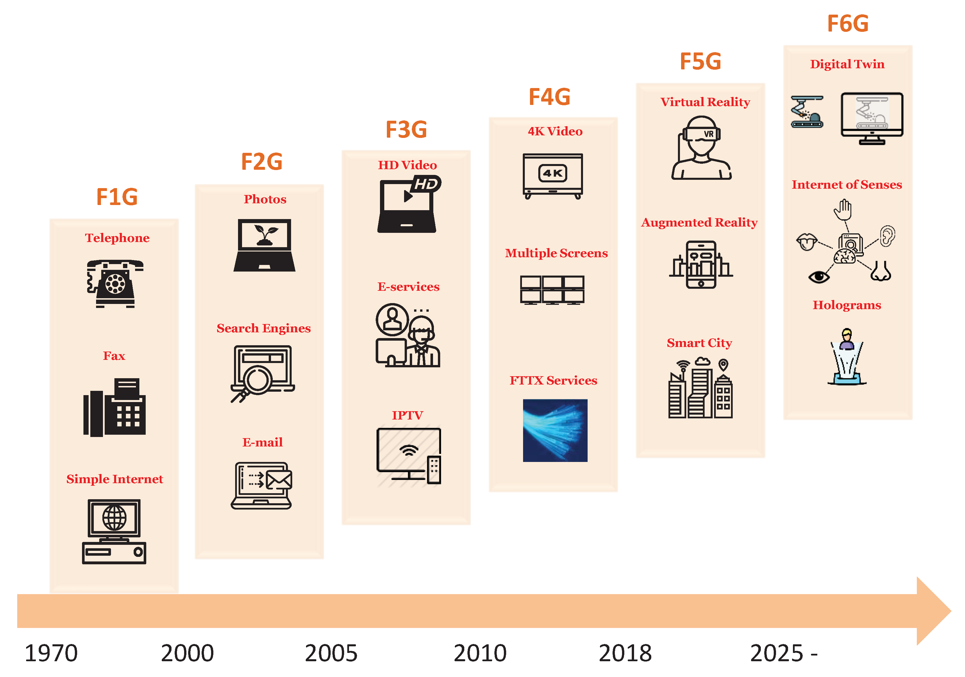
Figure 1. Representative services over the 6 fixed network generations as a result of 3rd Industrial Revolution.
Preprints 76390 g001
Figure 2. Our vision on the F6G ecosystem: the six categories of services based on their requirements.
Preprints 76390 g002
Figure 3. Service requirements during F5G and F6G.
Preprints 76390 g003
Figure 4. Conventional optical transceiver.
Preprints 76390 g004
Figure 6. The coherent 16-QAM constellation diagram attained using an AOSP based receiver [23].
Preprints 76390 g006
Figure 7. Comparison of the AOSP with alternative implementations for various quantities.
Preprints 76390 g007
Figure 8. Coherent transceiver alternatives for the different network domains.
Preprints 76390 g008
Figure 9. ADC Performance Survey 1997-2021 [34]. Illustration of the operational frequency of published ADCs versus the SNDR FoM. With the red solid/dotted lines is shown the Jitter FoM.
Preprints 76390 g009
Figure 10. Four major classes of photonic ADCs with their different variants.
Preprints 76390 g010
Figure 11. Photonic sampled and electronically quantized ADC.
Preprints 76390 g011
Figure 12. Conventional 64-QAM architecture where the light is split to the two parallel optical paths and it is modulated using a pair of MZMs.
Preprints 76390 g012
Figure 13. Segmented MZM (SEMZM) 7 segments oDAC architecture-optimized thermometer weighted DAC Structure for generation of PAM8 signals [19].
Preprints 76390 g013
Figure 14. (a) generalized parallel architecture proposed in [19] and (b) an implementation of PAM8 generator.
Preprints 76390 g014
Figure 15. (a) one of the two basic building blocks of the o-DAC [19]; (b) general architecture of the waveband selective switch, consisting of an adaptive filtering stage and an output port switch; (c) Structure of photonic lattice filter consisting of repeating blocks of tunable couplers and unit delay. These are implemented by MZI’s and prescribed length delay of DL (inset); (d) Normalized frequency response of an FIR filter having 38 filter taps.
Preprints 76390 g015
Figure 16. Global IP traffic demands (source: Cisco).
Preprints 76390 g016
Figure 19. Evolution of bit rate in the downstream direction for various PON standards and the road towards 100G PON.
Preprints 76390 g019
Figure 20. BER performance versus laser-linewidth when QPSK is employed [81]. CPE: common phase error, OBE: orthogonal basis expansion.
Preprints 76390 g020
Figure 21. Examples of a) geometric and b) probabilistic constellation shaping [83].
Preprints 76390 g021
Figure 22. Gain and noise figure of indicative available doped fiber amplifiers assuming a total input power in each amplifier equal to 0 dBm [71].
Preprints 76390 g022
Figure 23. Experimental results on transported capacity vs transparent reach for UWB transmission based on [89,90,91,92,93,94,95,96,97,98,99,100,101,102,103,104,105,106,107,108,109,110,111,112,113].
Preprints 76390 g023
Figure 24. Different SDM options in comparison with standard single mode fiber [13].
Preprints 76390 g024
Figure 25. RPF systems which are expected to be in use in all future subsea cable systems [134].
Preprints 76390 g025
Figure 26. Schematic illustration of a Submarine OADM node [134].
Preprints 76390 g026
Figure 27. Transportation capacity of submarine cables with and without SDM.
Preprints 76390 g027
Figure 28. SDM based Optical Distribution Network (ODN). OBFN: Optical Beamforming Network, PD: Photodiode, BBU: Baseband Unit, AroF: Analog Radio over Fiber [135].
Preprints 76390 g028
Figure 29. Multi-Pb/s TRx block diagram in an UWB-SDM scenario for future 6G networks.
Preprints 76390 g029
Figure 30. Data rate per TRx vs number of multiplexing Degrees of Freedom.
Preprints 76390 g030
Figure 31. Three ways to increase the number of transmitted data in an optical system.
Preprints 76390 g031
Figure 32. Prediction of transportation capacity (in Tb/s) based on currently deployed and planned submarine cables [13].
Preprints 76390 g032
Figure 33. Predictions of capacity times length product (in Pb/s.km) based experimental studies.
Preprints 76390 g033
Figure 34. High level representation of the industrial switching network for inter- (OXC-XF) and intra-factory (OXC-IF) connectivity.
Preprints 76390 g034
Figure 35. Evolution of optical switching over time.
Preprints 76390 g035
Figure 36. Multi-Granular Wave Band Selective Switch.
Preprints 76390 g036
Figure 37. Generalized architecture of a node with SDM/UWB functionality.
Preprints 76390 g037
Figure 38. (a) Route and select topology implemented with WBSS between ingress and egress fiber ports. (b) Multi-granular optical node enabled with interconnecting OXC for access to emerging full-band add and drop transceivers, as well as WDM level granularity with existing WSS technology in support of legacy transmission.
Preprints 76390 g038
Figure 39. High level representation of our vision on the I4.0 inter- and intra-factory connectivity.
Preprints 76390 g039
Table 1. Classification of services and their requirements in the F6G ecosystem. eFBB: Enhanced Fiber BroadBand, FFC: Full Fiber Connection, GRE: Guaranteed Reliable Experience, FFBC: Full Fiber BroadBand Connection, GRFB: Guaranteed Reliable Fiber Broadband, GRFFE: Guaranteed Reliable Full Fiber Experience.
Service Requirements Service Type
Category Service Bandwidth Latency Reliability Density eFBB FFC GRE FFBC GRFB GRFFE
Industry 4.0 Digital twins H L H M x
Harsh environment automation M L H M x
Collaborative robots H M H M x
AR diagnostics and collaboration H L H M x
AI and edge computing aided decisions H M H M x
Entertainment/
Communications
Holographic communications H M M L x
Immersive extended reality (XR) H M M L x
Internet of senses M M M L x
Transportation Ultra smart airport H L H H x x
Ultra smart port H L H H x x
Ultra smart highway H L H H x
Ultra smart city H L H H x
Ultra smart railway H L H H x x
Seamless monitoring, e.g. airplanes, fleet H L H H x x
E-Health Telesurgery H L H L x
AR field medical support H L H L x
remote areas Diagnosis/consultations H L H L x
Education AR assisted remote education H L H L x
Safety Health hazard monitoring H M H M x
AI assisted incident detection H M H M x
Table 3. Quantitative comparison of options for the optical sampling process of the RF signal [40].
Preprints 76390 i001
Table 5. Traditional vs. SDM Submarine Cables for various metrics [134].
SDM Cable Traditional Cable
Submarine Cable More fibers (12, 16, 24 FPPs and more in future) 6 FPPs and maximum 8 FPPs
Fiber Effective Area ( Aeff ) Low effective area. Aeff = 80-110 μm2, a = 0.15-0.16 dB/km High effective area, Aeff = 125-150 μm2, a = 0.15 dB/km
Repeater Type Repeater pump farming Each fiber has its own laser pumps
Branching Unit ROADMs Fiber pair switching in branch units No fiber pair switching in Branching unit ROADMs
OSNR Lower OSNR High OSNR
Modulation Formats PCS (Probabilistic Constellation Shaping) BPSK, QPSK, 8-QAM and 16-QAM
C+L Band Technology Currently restricted in C-Band C+L Band supported up to 144 channels fiber/pair
PFE Same PFE, capacity (Maximum 15 kV) Same PFE
Table 6. Qualitative Comparison of UWB and C-band SDM systems.
Ultra-Wideband (UWB) Space Division Multiplexing based on fiber bundles (Bu-MF)
Cost Significantly lower costs than SDM in cases of limited fiber availability Lower component associated costs when mainly C-band is exploited
Connectivity and reach Increased connectivity and flexibility as each band can be exploited for different transmission length Higher transparent length as C-band shows the best physical layer performance and the fibers/components have optimized performance
Upgradeability Very high considering a pay as you grow policy Very high considering a pay as you grow policy
Diversity A diversity in data rate per channel and reach can be attained by tailoring each band to specific requests (e.g., lower bands to shorter links and higher bands to longer ones) All channels are considered as “premium”, so a diversification in terms of data rate per channel and reach cannot be considered
Commercialization Mainly C and L bands Well established commercially available technology in C-band
Spatially integrated network elements Only when UWB amplifiers are used, e.g. Raman, SOA > 100 nm, C + L EDFA Possible, e.g. shared amplification pumps among the various fibers and lasers at the transceiver sides
Best solution for terrestrial networks access/DCI, submarine networks
Table 7. Main KPIs for intra and inter factory switches.
KPI Inter-Factory Intra-Factory
Capacity Fronthaul: up to hundreds of Gb/s
Tb/s scale
End point Data rate up to 2Gb/s; P2MP with 64 or higher end points
Latency End to end latency: < 100 μs End to end latency: 10 μs (excluding fibre propagation)
Reliability Very high 99.999 % (of packets)
Power Consumption few Watts per Tb/s few Watts per Tb/s
Cost 50 cents per Gb/s 50 cents per Gb/s
Electromagnetic interference resiliency Required Required
Jitter End-to-end jitter: 30 ns to a few μs depending on the application 30 ns to 50 ns
Dynamics ms-timescale P2MP can be with fixed BW allocation
Guaranteed Delivery End-to-end Packet loss rate: < 10-10 BER: < 10-5 (FEC with optimized latency)
Densification/Scalability Number of competing time sensitive flows: > 100
Number of machines in each edge cloud: ~200
P2MP aggregates the traffic of 64 end points into a single head end – increase density
Scalability could be provided by the use of WDM
Disclaimer/Publisher’s Note: The statements, opinions and data contained in all publications are solely those of the individual author(s) and contributor(s) and not of MDPI and/or the editor(s). MDPI and/or the editor(s) disclaim responsibility for any injury to people or property resulting from any ideas, methods, instructions or products referred to in the content.
Copyright: This open access article is published under a Creative Commons CC BY 4.0 license, which permit the free download, distribution, and reuse, provided that the author and preprint are cited in any reuse.
Prerpints.org logo

Preprints.org is a free preprint server supported by MDPI in Basel, Switzerland.

Subscribe

© 2024 MDPI (Basel, Switzerland) unless otherwise stated