1. Introduction
Lanthanides are a group of fifteen metallic elements in the periodic table. According to the selection rule, the f−f transitions are Laporte forbidden, so their trivalent ions (Ln
3+) are highly stable when incorporated into the host lattice (ligands). The surrounding crystal field developed by the host material destroys the spherical symmetry of the electronic structure, promoting the transition of an electron from a lower energy f orbital to a higher-energy f orbital. This process is called an induced electric dipole (ED) transition [
1], which gives rise to optical absorption and emission. Three types of transitions are possible when the lanthanide ion is under the influence of a ligand-field [
2]: f−f transitions, the transfer of a 4f electron into a 5d subshell, called hyper-sensitive or sometimes pseudo-quadrupolar transition because they apparently follow the selection rules of electric quadrupolar (EQ) transitions and charge-transfer (CT) transitions (metal to ligand or ligand to metal).
A significant advancement in lanthanide chemistry occurred with the introduction of cryptand ligands, which effectively enclose the lanthanide ion, safeguarding it against solvent molecules that dampen its emission [
3]. When the arms of the cryptand incorporate light-harvesting units, they function as an antenna, capturing light and transmitting the energy to the lanthanide ion. The creation of antenna systems centered around lanthanides, which enable the collection and conversion of light to different frequencies, holds significant implications for the advancement of photonic devices and sensors. Lanthanides (III) have unique optical properties that make them potentially useful in areas such as lighting [
4], biological imaging [
5], and solar energy conversion [
6], where the wavelength-converting materials can be incorporated into either the solar cell architecture or a luminescent solar concentrator [
7].
Despite their poor spectral response in short-wavelength regions of the solar spectrum (mainly due to thermalization losses from the absorption of high-energy photons [
8], the high reflective index, and shallow penetration depth of UV-blue irradiation (e.g. less than 100 nm for 400 nm wavelength) [
9]), solar cells such as Si, GaAs, CIGS or CdTe can still be improved. The most promising approaches to improving the short-wavelength response are the use of luminescent down-shifting (DS) and down-conversion (DC) layers [
10,
11]. DS is a process where one low-energy photon is created by one high-energy photon absorbed (one-to-one photon process) [
12]. DC is a one-to-two photon process, where a high-energy photon is split into two lower-energy photons. Quantum cutting [
13] is one approach to DC because a single photon with higher energy can be split into two photons with similar wavelength, and the theoretical quantum efficiency is above 100% [
14]. However, no experimental proof has yet been reported to demonstrate an efficiency gain using DC materials at the top of a c-Si cell. Theoretical studies predict a maximum conversion efficiency of around 40% [
15,
16], due to the low absorption cross-section of the downconverters.
Despite not exceeding 100% efficiency, down-shifting can be used to improve PV efficiency. By shifting the photons with shorter wavelengths to lower energy, they can be absorbed more effectively by solar cells. Rare-earth organic complexes are an important class of DS materials for PV modules [
10]. Unlike organic dyes or fluorophores [
17] and semiconductor quantum dots (QD) [
18], lanthanide complexes are stable, have large Stokes shifts, and avoid self-absorption losses, where the luminescence process occurs in three steps (
Figure 1), [
19].
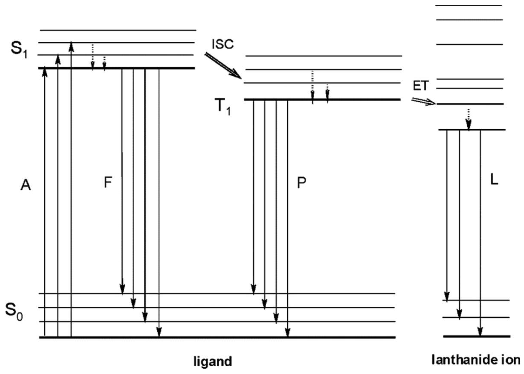
The photophysical process for emission begins with the absorption of light by appropriate ligands, which undergo a transition from their fundamental singlet state (S
0) to an excited singlet state (S
1). An efficient intra-energy conversion from the singlet (S
1) to the triplet (T
1) states of the ligand occurs through nonradiative intersystem crossing (ISC), followed by resonant energy transference (ET) from the T
1 state of the ligand to the excited state of the Ln
3+ ion, which transitions to one of its emissive levels [
20,
21]. The excited singlet state can be deactivated radiatively to the ground state (molecular fluorescence), and the triplet state T
1 can be deactivated radiatively to the ground state, by the spin-forbidden transition T
1 → S
0 (molecular phosphorescence).
Our group has been working on luminescent DS rare-earth-based compounds in recent years. C1–6 complexes [
22,
23,
24,
25,
26,
27,
28,
29] use ternary europium (III) complexes embedded in poly(methyl methacrylate) (PMMA), and C12–17 [
30] are mixed-ligand bimetallic complex prepared with the ions Eu
3+, Gd
3+ and Tb
3+ embedded in ethylene-vinyl acetate (EVA) as a down-shifting material for silicon-based solar cells. C7–11 complexes [
31] were also prepared with other lanthanide (III) ions, and preliminary studies on their photophysical processes involved in photoluminescence were conducted.
Several methods have been documented in literature for integrating LDS layers into solar structures. These include spin-on coating techniques [
32], deposition of lanthanide-based DS layers on c-Si PV using ethylene-vinyl acetate (EVA) [
33], incorporation of Eu(III) or different luminescent organic dyes in the encapsulants [
34,
35,
36,
37], re-optimization of the AR-coating [
38], implementation of planar luminescent DS layers [
39], utilization of CASN:Eu
2+ in PMMA [
40], and inclusion of the DS layer in the encapsulation process [
41], among others. Although it is not the subject of this work, we want to mention that lanthanide ions are also involved in up-conversion processes [
42], in which emission occurs at higher energy than the excitation (anti-Stokes phenomenon).
The external quantum efficiency (
EQE) serves as a measure to assess the improvement achieved by employing DS layers in solar cells.
EQE is defined as the ratio of the number of electrons produced by the device to the number of incident photons at each wavelength. This parameter helps evaluate the losses that contribute to the reduction of the measured short circuit current density (
JSC) from the maximum achievable photocurrent [
43].
Integrating lanthanide downshifting layers into solar cells poses several challenges that must be addressed, including cost-effectiveness, stability, and efficiency [
44,
45]. As solar energy continues to grow in importance as a renewable energy source, advancements in downshifting will play an increasingly crucial role in addressing these challenges [
46,
47,
48,
49,
50,
51,
52,
53,
54,
55,
56,
57,
58,
59,
60,
61,
62].
This work discusses the research we have conducted on UV degradation, conversion efficiency, and photoluminescence studies of lanthanide ions as spectral downshifters for solar cells to tackle these challenges. The development of this work is structured firstly with the materials and methods used to synthesize and characterize the studied complexes. Next, the obtained results are detailed, including structure, preparation of down-shifting films, absorption spectrum, and photoluminescence. Finally, these DS films are applied in different photovoltaic devices, obtaining results of external quantum efficiency in different cases. We also include studies conducted on UV degradation of these DS films and, ultimately, perform various studies on bifacial photovoltaic cells.
3. Results and discussion
3.1. Synthesis and characterization of the complexes
The synthesis of all compounds, except for C4, has been previously described in our prior works [
22,
23,
24,
25,
26,
27,
28,
29,
30,
31]. For the purpose of discussing the general synthesis strategy of these compounds, we will focus on the synthesis of the new compound C4. The compound [Eu(bta)
3pyz-phen] (C4) is obtained by the reaction of stoichiometric quantities of Eu(NO
3)
3·5H
2O, pyz-phen, Hbta, and triethylamine (C
2H
5)
3N), (99%). 1-benzoyl-3,3,3-trifluoroacetone (C
10H
7F
3O
2) (648 mg, 3 mmol) was dissolved in 40 ml of ethanol, and the solution was heated at 65°C under stirring. Then, (C
2H
5)
3N) (416 μL, 3 mmol) was added under stirring. Subsequently, a solution of pyz-phen (208 mg, 1 mmol) in ethanol (4.0 ml) was added. In a separate container, Eu(NO
3)
3·5H
2O(425 mg, 1 mmol) was dissolved in ethanol (10 ml). Finally, both solutions were mixed and stirred for 3 hours. After that time, 50 ml of water was added, and a white product was obtained, which was filtered, washed with water, and dried in an oven at 60°C overnight (yield, 92%).
The compounds were prepared under a dinitrogen atmosphere in order to avoid oxidation of the reagents. All compounds were prepared from stoichiometric amounts of their components. Initially, the syntheses were carried out in water, but we have found higher yields when the synthesis is performed in ethanol. Ligands with diketonate groups need to be deprotonated to obtain the corresponding diketonate, and the best result is achieved using triethylamine as a base. The optimal reaction time is 180 minutes. The crude product can be obtained by the addition of water, but it is highly recommended to recrystallize it by liquid-vapor diffusion. Chloroform, THF, or acetonitrile can be used as solvents, and n-hexane or n-heptane as precipitating agents. By using these procedures, single crystals and powder can be obtained, which are characterized by X-ray diffraction techniques. The purified products are used for photoluminescence measurements and film preparation.
3.2. Structure of the complexes
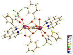
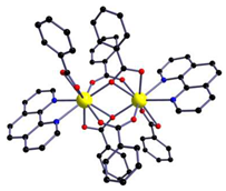
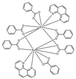
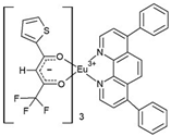
We have added the diffraction patterns of the different compounds as supplementary material (Figures S1-7). The structure of the compounds C1 and C2 consist of centrosymmetric dinuclear molecules in which each Eu atom is bound to one phenanthroline or bephenanthroline molecule and one terminal bidentate benzoate ligands (
Table 1). The powder diffraction pattern and selected distances of C1 and C2 can be found in previous works [
22,
23]. These complexes crystallize in the triclinic system, space group
P1.
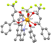
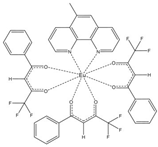
The asymmetric unit of compound C4 contains two different molecules of the complex C5 which are stereoisomers. The two molecules have the same organic ligands, the same coordination number, and the same coordination environment of the central Eu(III) ion. However, the two molecules differ in the relative orientation of one of the bta- ligands. C4 and C5 complexes crystallize in the orthorhombic Pna21 and Pbca space-groups, respectively. The complex C6 crystallizes in the monoclinic P21/c space-group with its Eu(III) ion bound to one 5-methyl-phenanthroline and three β-diketonate benzoyl trifluoroacetone ligands.
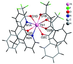
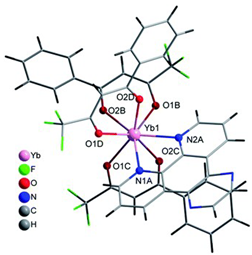
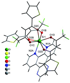
Structures of C7-11 complexes are shown in
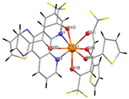
Table 2. The crystal structure of C8 was solved by single-crystal X-ray diffraction and it was found to be isostructural with the corresponding C7 and C9 complexes. C8 complex crystallizes in the monoclinic P21/c space-group and has a molecular structure in which the Yb(III) ion is bound to six oxygen atoms of three β-diketonate bta- ligands and two nitrogen atoms of one 5-methyl phenanthroline ligand. C10 crystallizes in the orthorhombic
Pna21 space-group and has a molecular structure with the Yb atom surrounded by three bta- β-diketonate ligands and one 2,3-pyrazine-1,10-phenanthroline ligand. C11 crystallizes in the orthorhombic
Pbca space-group, and its molecular structure is formed by Er(III) ions surrounded by three tta- β-diketonate ligands and one pyz-phen ligand.
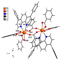
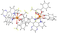
In the case of [M1M2(bz)4(tta)2(phen)2] series, PXRD patterns confirmed that all compounds were isostructural. The structure of C12, solved by single-crystal X-ray diffraction, showed that these complexes crystallize in the triclinic space-group as neutral centrosymmetric dinuclear molecules of [M1M2(bz)4(tta)2(phen)2] with four bridging benzoate (bz−), two 2-thenoyltrifluoroacetonate (tta−) and two 1,10-phenanthroline (phen) ligands.
Table 3.
Molecular structures of the C12–17 complexes [M2(bz)4(tta)2(phen)2], where M2 metal- ions can be Eu2, Gd2, EuTb or EuGd..
Table 3.
Molecular structures of the C12–17 complexes [M2(bz)4(tta)2(phen)2], where M2 metal- ions can be Eu2, Gd2, EuTb or EuGd..
| Complex |
Molecular structure |
[Eu2(bz)4(tta)2(phen)2] (C12) (*)
|
 |
3.3. Preparation of the luminescent down-shifting layers
Samples containing 1–7 mg of the C1–2 complexes were dissolved in 7 mL of CH2Cl2 in a refrigerated ultrasonic bath; (ii) then 70 mg of PMMA were added and the mixture stirred until complete solution of the polymer, obtaining samples with relative concentration of the actives species ranging from 1.4 to 10%; (iii) spin-coating method was used for film deposition (50-100𝜇m) on commercial glass substrates.
An analysis of the additional costs of a solar panel with this type of film can be seen in previous studies [
22], where we estimated in euros (€) per square meter (m
2) of solar panel with 15% efficiency, at approximately 0.05 €/m
2 for every 1% of complex product used. However, these costs were calculated in 2015, and the prices of the chemicals used have increased significantly nowadays. Thus, for complex C1, we have made an estimate of its price per square meter for the same concentration, resulting in approximately 0.48 €/m
2. For the other complexes, we have also estimated their price in euros per square meter for a 1% concentration, from lowest to highest price for the C1-6 series as follows: C1=0.48; C6=0.84; C5=1.24; C4=1.28; C3=1.71; C2=2.28. For the C7-11 series, C7=0.56; C8=0.58; C9=0.61; C11=0.97; C10=1.02. And for the C12-17 series, C13=0.16; C15=0.32; C16=0.36; C14=0.37; C17=0.42; C12=0.49.
To obtain the DS layers corresponding to complexes C3, C7 and series C12-17 before were encapsulated on a PV mini-module, Deltalab 1.1 mm thick EUROTUBE® Slides (25 mm × 70 mm) were cut into 20 × 20 mm squares or 25 × 20 mm pieces and immersed in a 2 M sulfuric acid solution for one hour, rinsed with a generous amount of deionised water and dried at 60 °C overnight. 10 mg of DS complex mixed with 25 mg of EVA was dissolved in 1.5 mL of CH2Cl2 under vigorous stirring for 20 min. 300 µL of that solution was dropped on the glasses and the solvent was evaporated at room temperature.
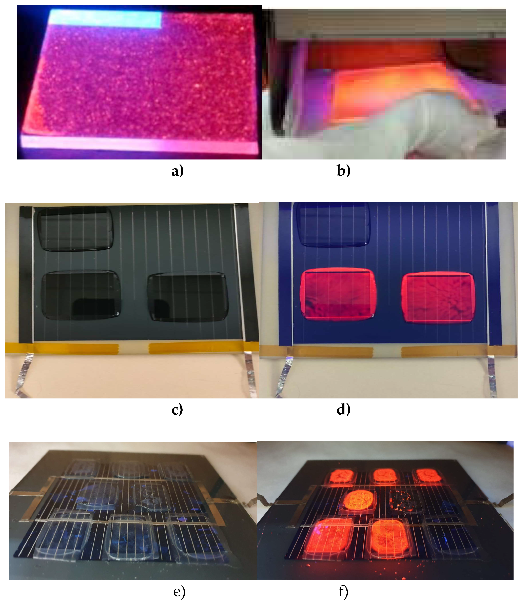
Figures 2a) and b) display the down-converting layers of C1 and C3 complexes, respectively, which are embedded in PMMA and deposited on bare glass substrates under UV radiation. The C3-7 and C12-17 series samples were encapsulated using a standard procedure [
65] with the Lab PV Module Laminator from Fraunhofer ISE. Examples of the C3 complex can be observed in Figures 2c) and d) when exposed to UV light. Figures 2e) and f) demonstrate the down-converting layers of C12-17 complexes embedded in EVA, both without and with UV light.
Figure 2.
Images of downshifter layers corresponding to complexes C1 a) and C3 b) when irradiated with ultraviolet light. In photograph c), downshifter layers of complex C7 laminated with EVA are observed on a mini module of copper indium gallium selenide (CIGS), and in photograph d) when illuminated with UV light. Photograph e) shows converter layers from the C12-17 series laminated with EVA on a multicrystalline Silicon mini module, and in photograph f), the same samples when irradiated with UV light.
3.4. UV-vis absorption spectra
By using the values obtained for the absorbance A, using the UV-visible spectrometer specified in the general methods, along with the concentration of the absorbing species per unit volume c [M = mol/L] and the distance that the light travels through the solution l [cm], we can determine the molar absorptivity ε = (A/lc) [M-1 cm-1].
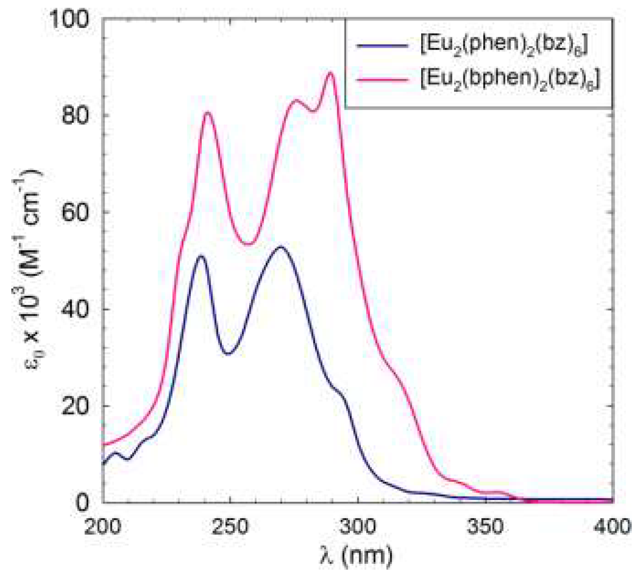
The UV-vis absorption spectra of the C1 and C2 complexes are presented in
Figure 3, where compared to C1, C2 shows an increase in the molar absorption coefficient ɛ, with a maximum at 290 nm. This increase is usually correlated with an increase in the emission since the bphen ligand itself exhibits higher absorption compared to phen.
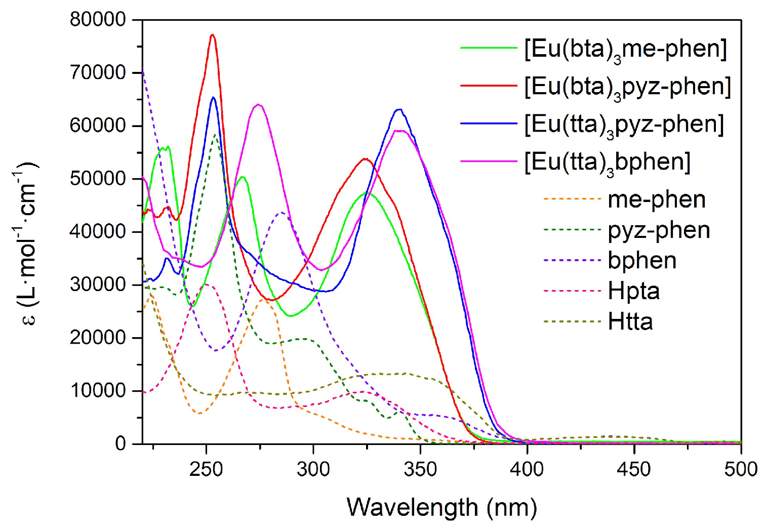
The UV-vis absorption spectra of the C3-6 complexes are shown in
Figure 4. They are considerably enhanced with respect to the ligand spectra since the complexes contain three molecules of the diketonate ligands plus the phenanthroline derivative. The pattern of the absorption of [Eu(bta)
3pyz-phen] and [Eu(bta)
3me-phen] complexes are very similar around 320 nm since all the compounds contain the same diketonate ligand and the contribution of the phenanthroline derivative is expressed at lower wavelengths. [Eu(tta)
3bphen] and [Eu(tta)
3pyz-phen] have a higher absorption coefficient at higher wavelengths due to the more intense absorption of the tta- ligands at higher wavelengths (340 nm). All the complexes have little absorption in the visible region, and diluted solutions are almost colorless.
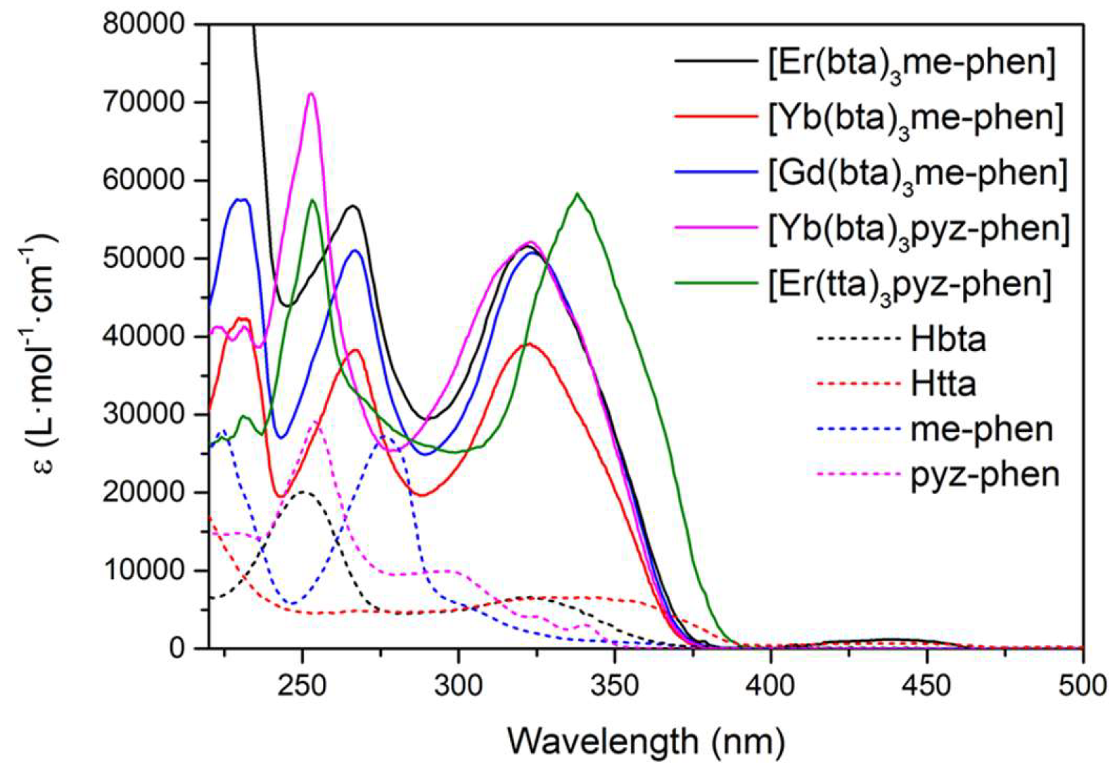
Figure 5 shows the ε vs λ spectra of C7-11 complexes together with the free ligands Hbta, Htta, me-phen and pyz-phen in the UV-vis region.
Complexes C7-10 have the same band at 320 nm due to the bta- ligands, while complex C11 presents a band at 340 nm corresponding with the absorption of the tta- ligands. Since these absorbances can be attributed to the S
0 → S
1 transition of the ligands, they give the energies of their singlet excited states, being in this case 26700 cm
-1 and 23500 cm
-1 for the bta- and tta- ligands respectively, which are values in agreement with those previously reported [
66]. The contribution of the phen-derivative ligands appears at lower wavelengths. Complexes C10 and C11 exhibit a maximum of around 250 nm due to the pyz-phen ligand and compounds C1-3 have two bands at around 230 nm and 270 nm corresponding with the maximums of the me-phen ligand.
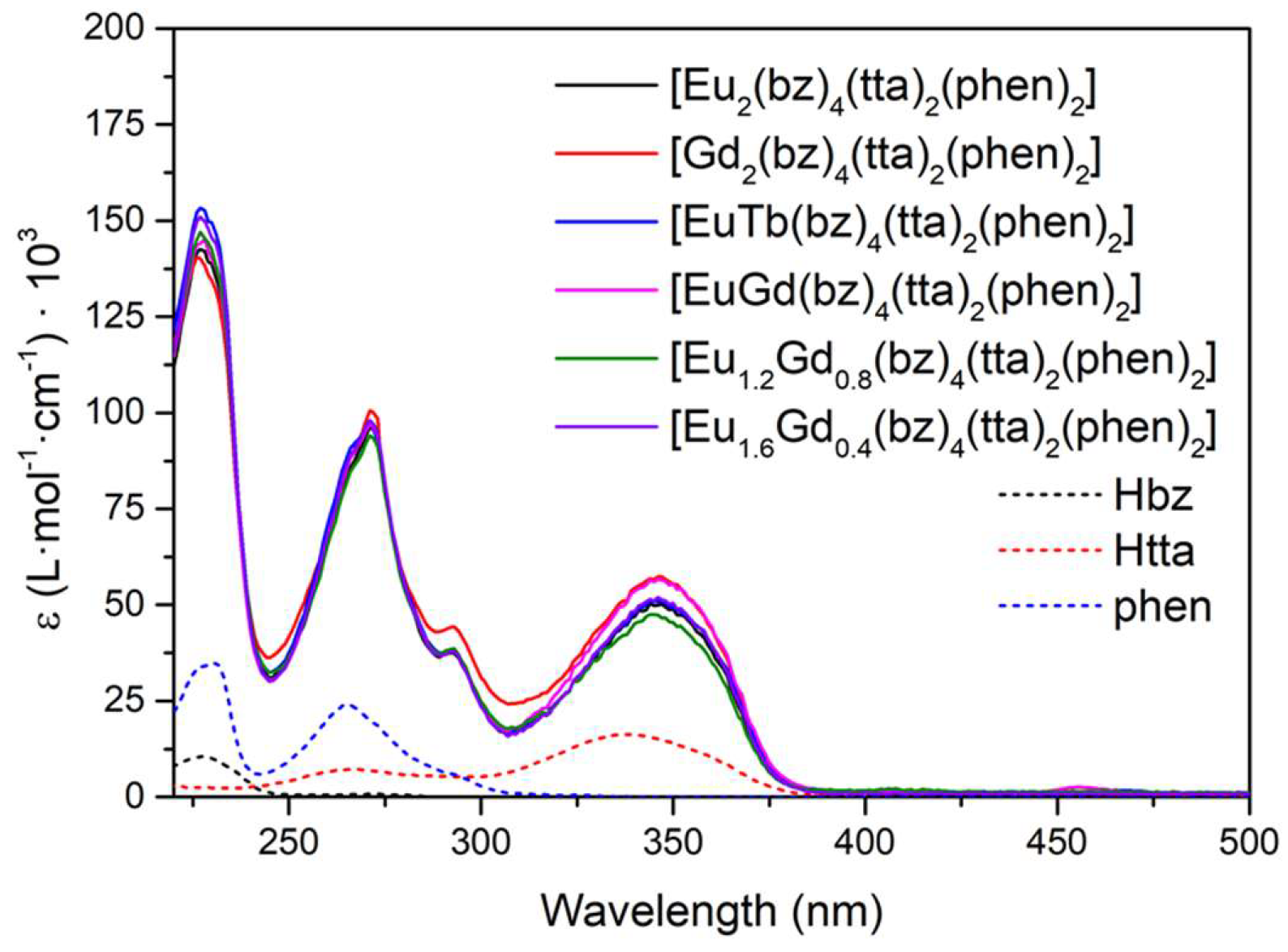
In the case of the [M1M2(bz)
4(tta)
2(phen)
2] complexes, all of them present the same pattern since they are analogous compounds with bz-, tta- and phen ligands (
Figure 6). The increase of complexes’ absorption compared to the free ligands is greater than in the previous compounds since each complex molecule contains two molecules of phen, four bz- molecules, and two β-diketonate tta- ligands. The first absorption band at 227 nm with a shoulder at 230 nm is due to the contribution of bz- and phen ligands, respectively. Phenanthroline molecules cause the second maximum at 271 nm with a shoulder at 292 nm, and the last band at 346 nm suffers a bathochromic shift concerning the absorptions of the tta- ligands at 336 nm.
3.5. Photoluminescence
Ternary complexes with β-diketonate ligands are a good choice of the organic antenna in order to observe efficient energy transfer from T1 to Ln
3+ ion, as many previous studies indicate [
67]. The derivatives of phenanthroline are also very efficient for their rigidity and the direct bond of the nitrogen atoms to the metal ion when the complex is formed. The photoluminescence quantum yield, also known as PLQY or Φ [
19], of a molecule or material is defined as the ratio of the number of photons emitted to the number of photons absorbed (internal PLQY). It is also important to know the fluorescence lifetime (τ) of a molecule, which is defined as the average length of time it spends in the excited state. These properties of a fluorophore or fluorescent molecules are crucial for understanding the behavior and interactions of many important materials at the molecular level. The dependence of the quantum yield on the influence of a ligand to metal charge-transfer state is determined by its energy level in relation to both the ligand and metal-ion levels, as well as the significance of the crossing over between this state and the excited and ground term manifolds of the Ln(III) ion [
3].
The studies of the UV-vis absorption and photoluminescence properties give us the necessary data to estimate the energy diagrams of the luminescence processes. This includes the energy of the excited states, the intersystem crossing (ISC) and the energy transfers (ET) of the down-shifting processes, among others. We have added the energy diagrams of the different compounds as supplementary material (Figures S8-12).
The photophysical measurements were performed with the samples as solids in order to avoid solvent effects. Photoluminescence excitation (PLE) and emission (PL) spectra of C1 in PMMA at 2.0 weight% (wt%) placed on glass is reported our previous work [
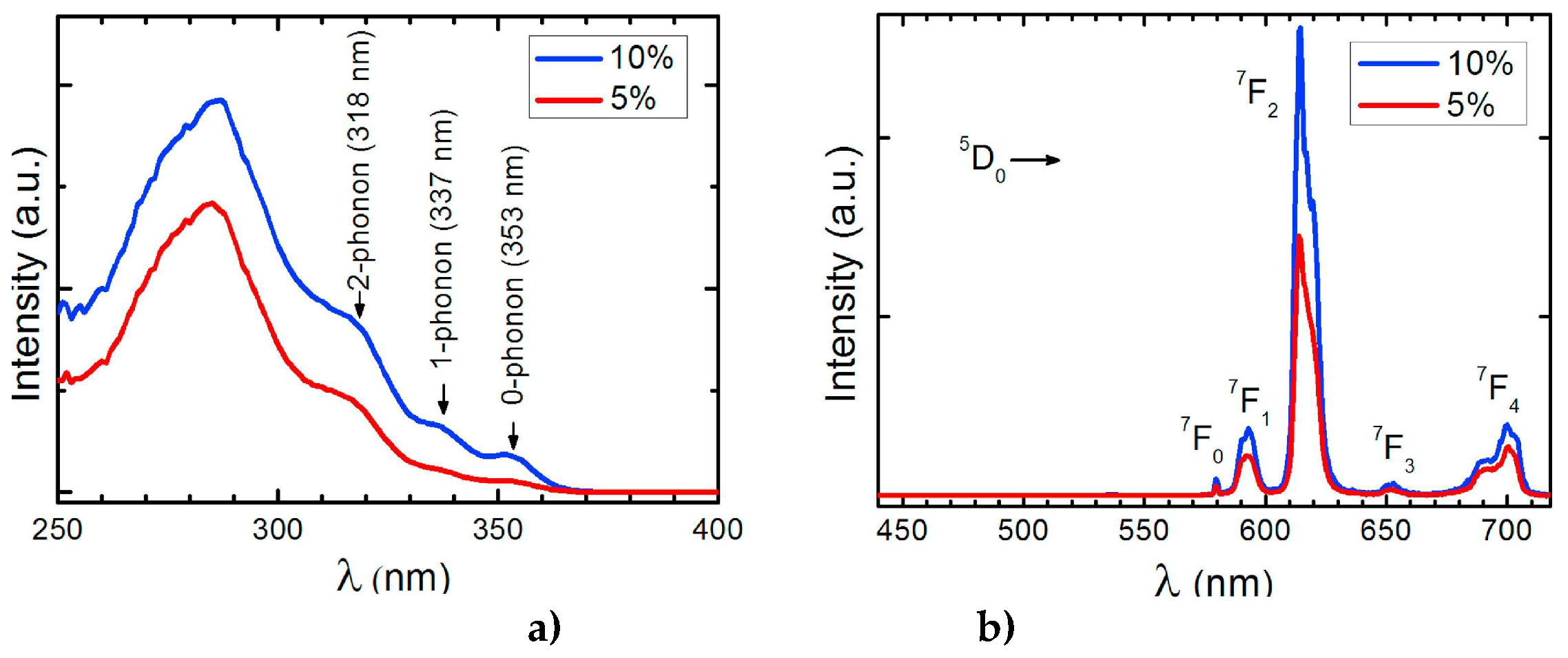
22], and the corresponding spectra of C2 at 5.0 wt% and 10 wt% in PMMA films, similar to C1 spectra, are shown in
Figure 7 [
23].
The excitation spectra of C2 display a broad band between 250 and 350 nm with a maximum at 280 nm. The emission spectra reveals the characteristic emission peaks of Eu3+ ion corresponding to the
5D
0→
7F
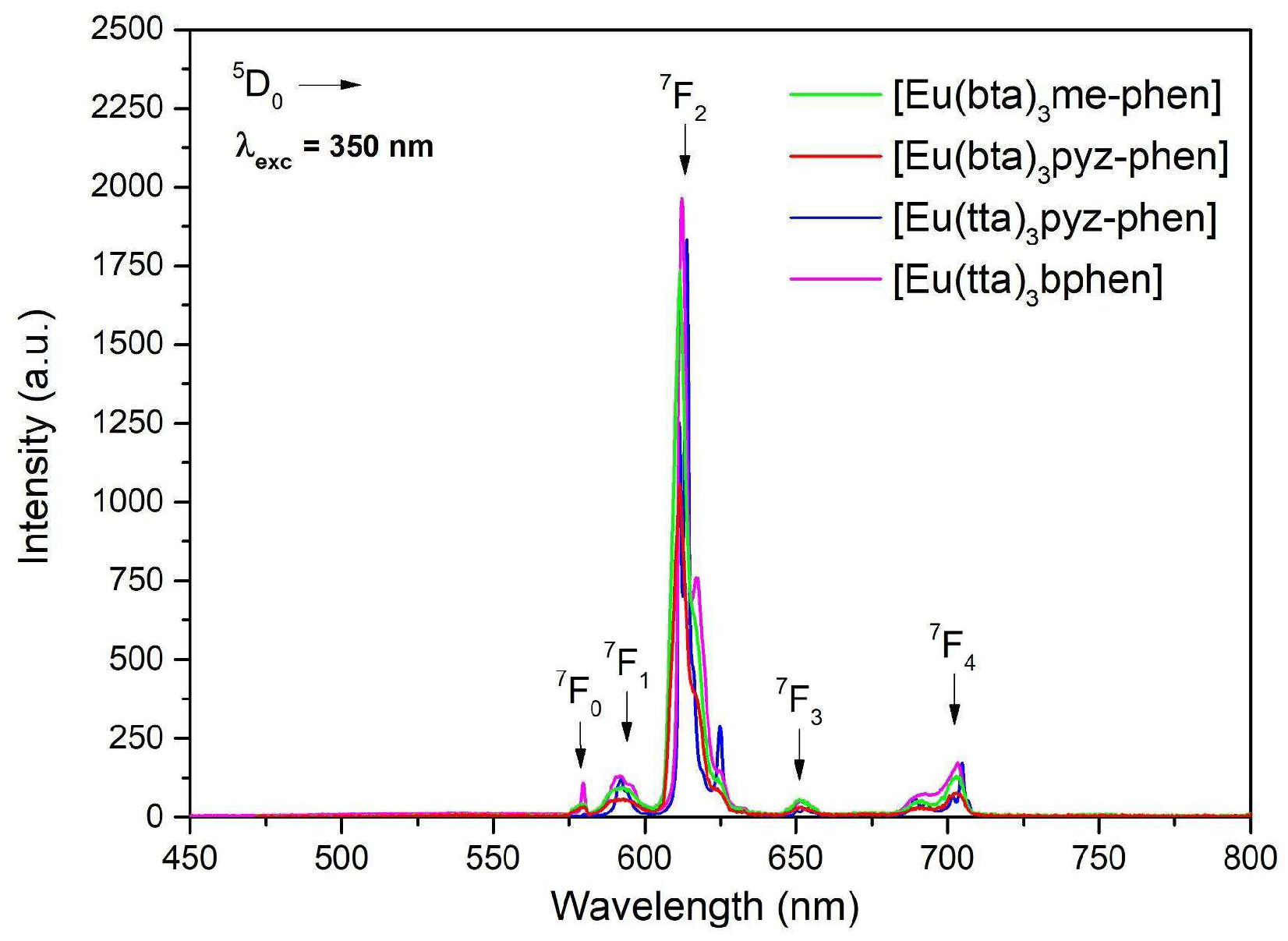
0-4 transition, being the emission at 614 nm the most intense transition. Analogue to this PL spectra, the emission spectra excited at 375 nm of the C3-5 complexes (
Figure 8) gave five sharp lines at 579, 590, 612, 652, and 701 nm, due to the
5D
0→
7F
0-4 transitions of Eu
3+. Of these transitions, the most intense is
5D
0→
7F
2 at 612 nm, which is responsible for the red emission color.
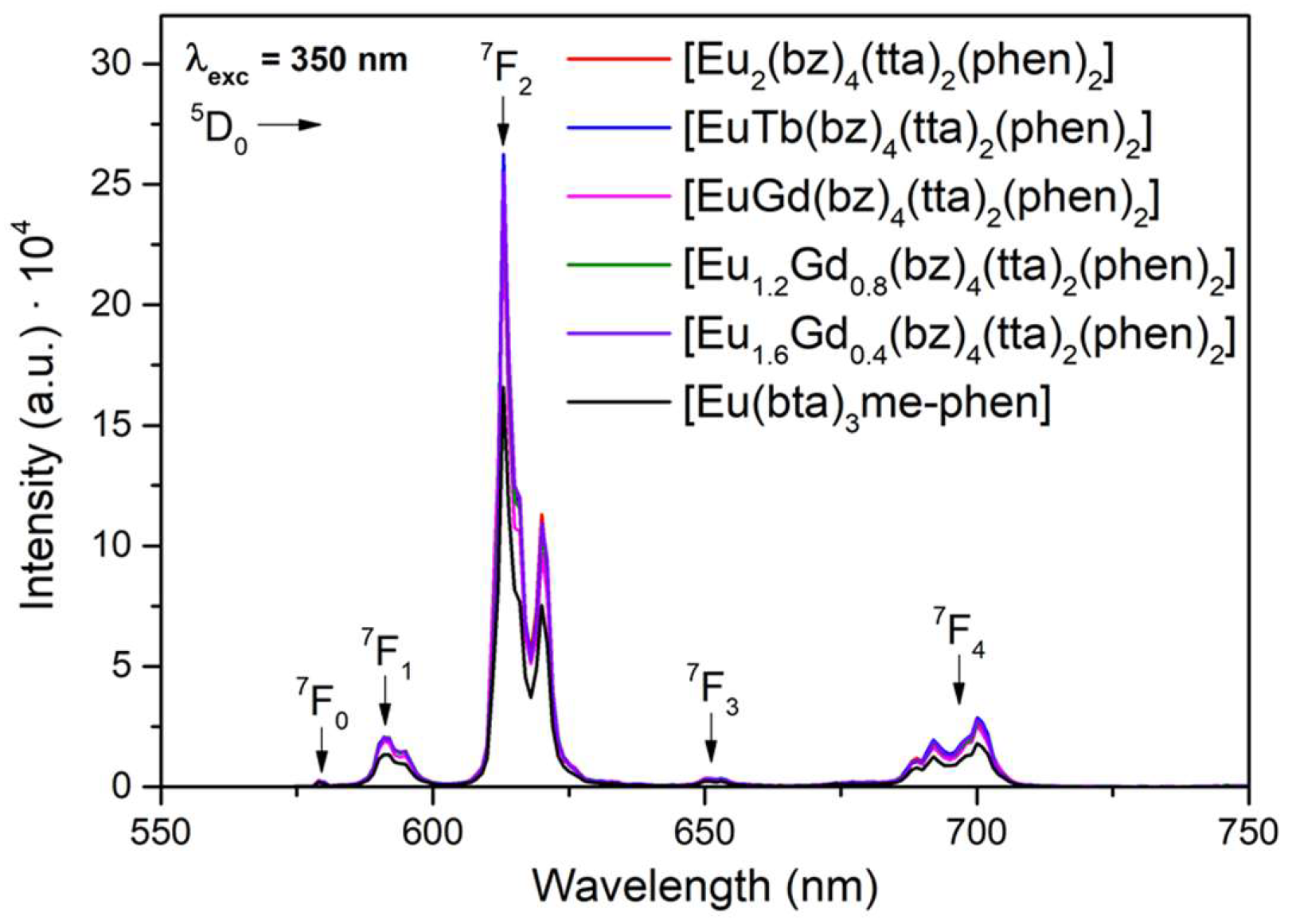
All the compounds C6, C12 and C14-17 containing the Eu(III) lanthanide ion exhibit intense emission with sharp peaks in the 570–730 nm range associated with the
5D
0 →
7F
0–4 transitions of the Eu(III) ion (
Figure 9).
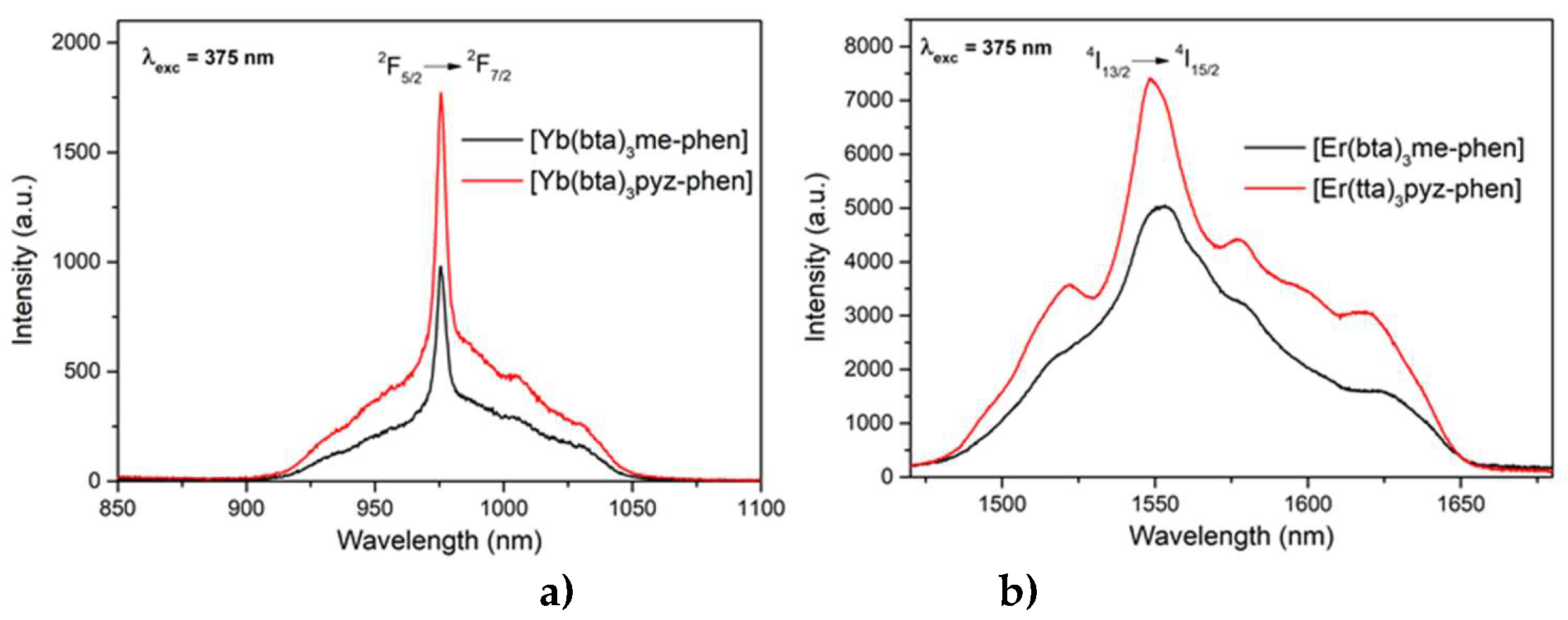
The C8 and C10 complexes, [Yb(bta)
3me-phen] and [Yb(bta)
3pyz-phen respectively, emission patterns were measured exciting at 375 nm, and show an intense NIR-emission centered at 980 nm that corresponds to the typical
2F
5/2 →
2F
7/2 transition for Yb(III) (
Figure 10 a)). The compounds [Er(bta)
3me-phen] and [Er(tta)
3pyz-phen] also have their principal emission band in the NIR, with a maximum at 1550 nm due to the
4I
13/2 →
4I
15/2 transition of the Er(III), when exciting at 375 nm (
Figure 10 b)).
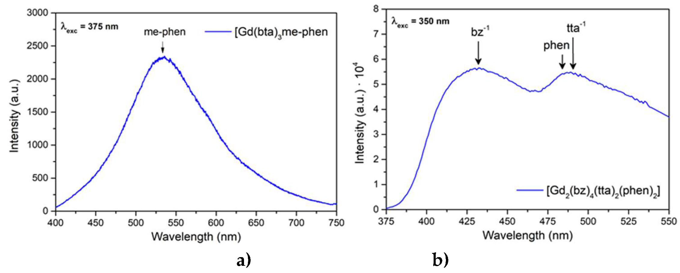
Figure 11 shows the emission patterns of complexes C9 and C13, [Gd(bta)
3me-phen] a) and [Gd
2(bz)
4(tta)
2(phen)
2] b), where the phosphorescence of me-phen, bz
-, tta
- and phen is observed. Normally, the energy of the excited levels of Gd(III) is above the energy of the excitation radiation or the energies of the excited states of the ligands. In this case, the excitation wavelength was 350 nm, that is 28 570 cm
-1, while the energy of the first excited state of Gd(III) (
6P
7/2) is around 32.500 cm
-1.
In
Table 4, we summarize the measured values of lifetime through intensity decays [
30,
68] and values of PLQY using indirect methods and an integrating sphere [
31] in some compounds. In some cases, although we have not yet measured these values, we did address their studies as downshifting layers in photovoltaic mini-modules, since the characterization of its photoluminescence had already demonstrated the suitability of the complex for PV applications.
3.6. EQE measurements
To quantify the effect of the DS layers on top of the PV devices, we calculated the increase in photo-generated current,
ΔJsc, as a function of the wavelength,
λ, through equation (1) [
71]
where q represents the charge of an electron, 𝜙 is the incident photon flux,
ΔSR is the increase in spectral response (SR), and
E0 is a standard reference of solar spectral irradiance based on ASTM G173-03 [
64]. The spectral response uses the power of the light at each wavelength, with its magnitude given in Ampere/Watt. Converting
EQE to SR is done using the formula
SR =
EQE(nm)/1239.8. Equation (1) was used to determine the current density
Jsc of the solar cell with DS films encapsulated. Estimations of the relative increase in conversion efficiency (
η), are made while considering that the open circuit voltage (
Voc) and the fill factor (
FF) remain constant when the downshifter is placed on the PV mini module. By assuming that (%) is equal to the product of
Jsc,
Voc , and
FF, for one sun of irradiation, the increment in relative percentage of conversion efficiency,
, can be calculated using the following expression
Below, we summarize the results we have obtained with the complexes used for different experimental configurations. In order to optimize our research on the use of DS films in different PV devices, we have been testing the placement of photoluminescent films on the device, the concentration of materials used in their manufacturing, the light concentration using spherical reflectors, the encapsulation of the photoluminescent films on the device, and the degradation they may undergo with prolonged exposure to ultraviolet light.
3.6.1. DS layers using different concentrations of complexes C1 and C2
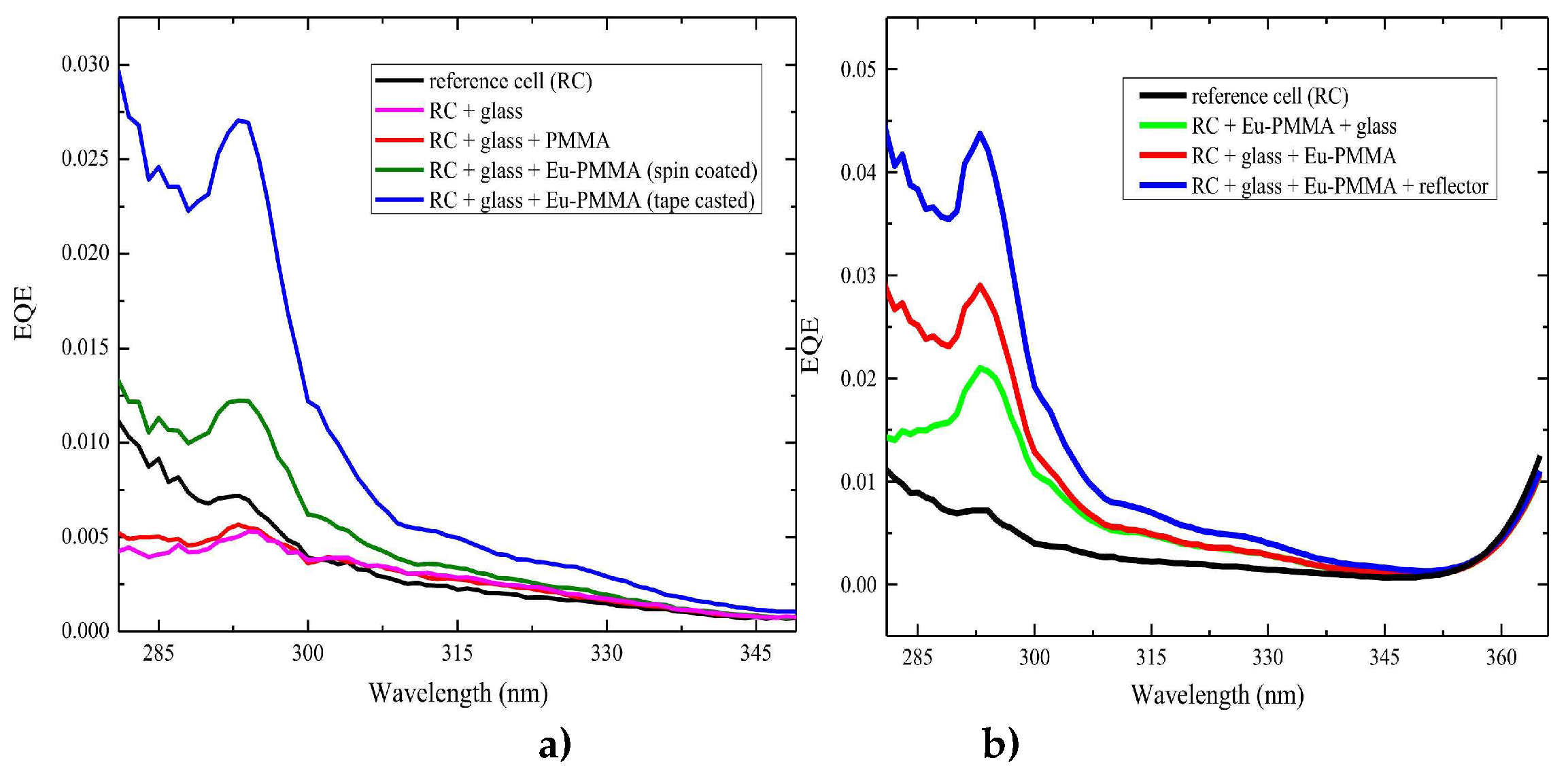
Figure 12 shows the measurements obtained in
EQE when using a DS film of complex C1 for different experimental configurations.
Figure 12 a) shows the
EQE behavior for the 280 – 350 nm spectral range when the DS layer was deposited through spin coating or tape casting on glass while
Figure 12 b) shows the wavelength dependence of the
EQE when the DS layer was deposited through tape casting on the rear side of the glass and covered by a UV reflector.
The analysis of the measurements obtained from
EQE with the DS film of complex C1 allows us to calculate estimates of the relative increase in percentage efficiency, as shown in
Table 5.
The values of (Δη/η) % are very high in the UV region where the photovoltaic device practically has no response. This increase is what can ultimately lead to a gain across the entire studied spectrum.
The C2 complex using the bphen ligand improves the absorption and photoluminescence results of the C1 complex, as shown by the results discussed earlier. The measurement of the
EQE of the device with DS films continued with higher concentrations of this C2 complex, as shown in
Figure 13 a) and b).
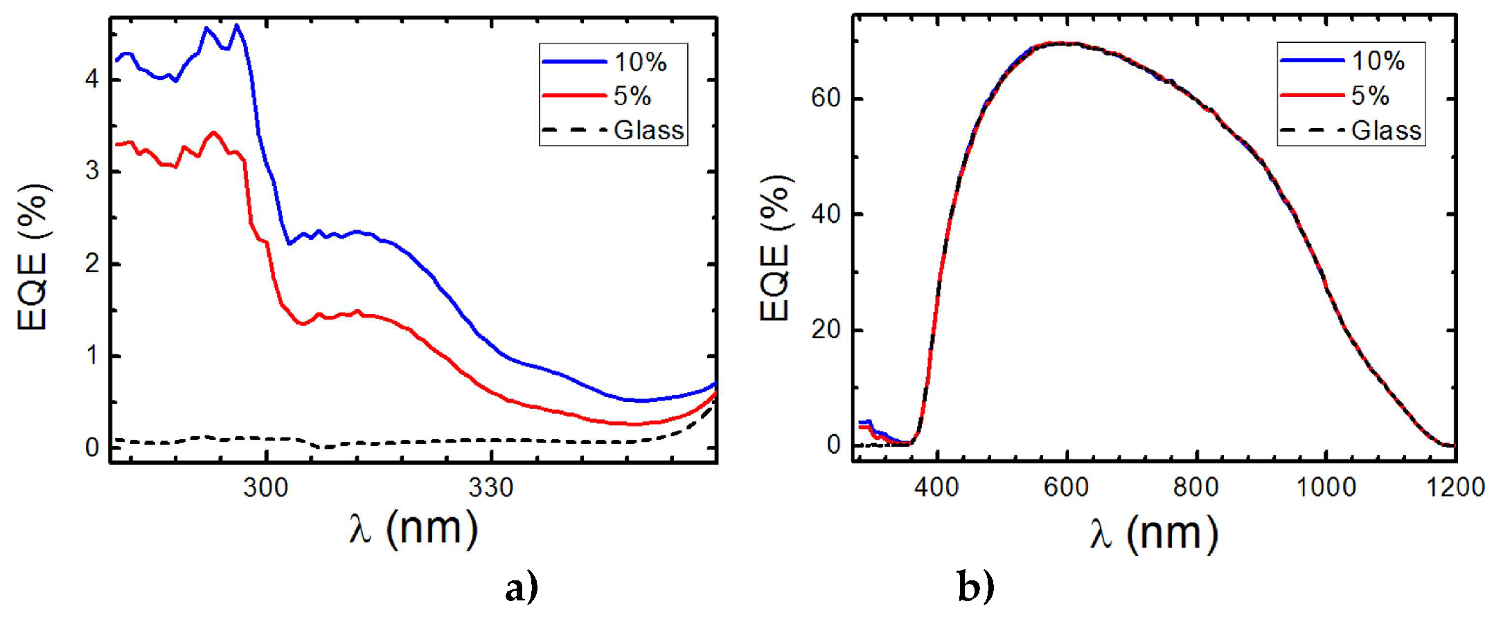
Figure 13 a) displays the obtained
EQE measurements for the UV region, where there is a maximum of 4.6% and 3.5% for C2 complex concentrations of 10% and 5%, respectively. The
EQE measurements across the spectrum shown in
Figure 13 b) demonstrate that these DS films do not worsen the efficiency in the visible region of the spectrum.
3.6.2. DS layers using different concentrations of complex C3
When the PV mini module used has virtually no response in the UV region, the
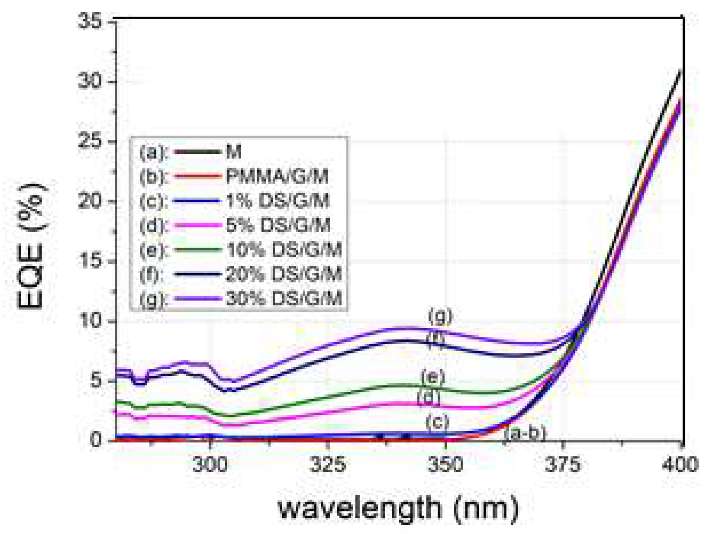
EQE values increase with the concentration of complex C3 when the DS film is placed on top. This evolution can be studied based on the obtained results shown in
Figure 14. Thus, for the maximum
EQE value at an excitation wavelength of 340 nm, it is found that there is a maximum concentration value of complex C3 in the DS film, close to 30%, as above that value the transmittance of the DS film decreases to zero.
The maximum downshifting efficiency is determined by increasing the concentration of the active species to its solubility limit [
25]. Our results are consistent with the
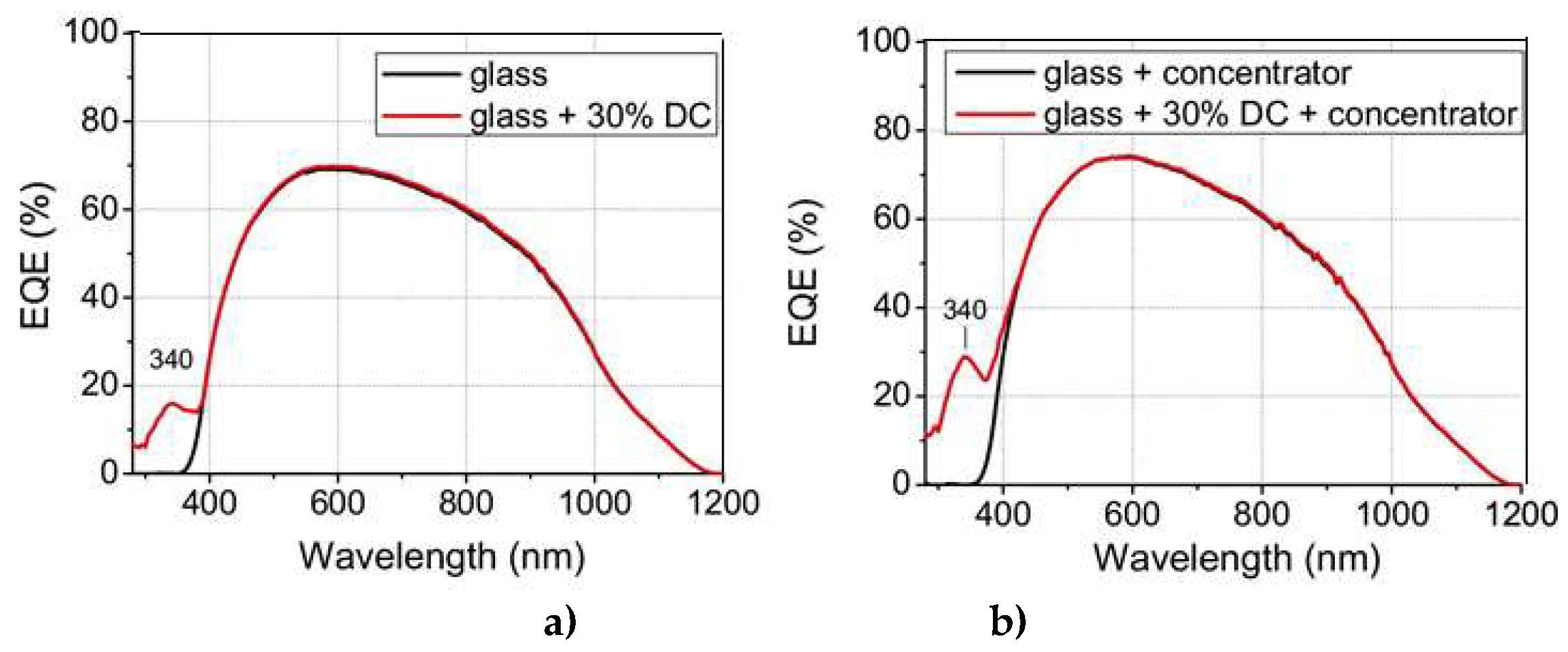
EQE behavior, as shown in
Figure 15.
The increments in the relative percentage of conversion efficiency from
Figure 15 a) were 1.07% and 1.92% for 10% and 30% concentrations of complex C3, respectively. For the PV mini module based on a single p-type mc-Si solar cell with a 16% conversion efficiency, the increases were 0.17% and 0.31%, respectively.
If we use the same configuration but add a hemispherical reflector (concentrator) on top of the downshifter to collect most of the downshifted photons emitted isotropically out of the device, we obtain EQE values as shown in
Figure 15 b). With a 30% concentration of complex C3, the relative percentage of conversion efficiency increased by 2.88% and the absolute conversion efficiency increased by 0.46%. This new configuration can be integrated into PV devices for specific applications related to concentrator photovoltaics
3.6.3. DS layers using complexes C4-6
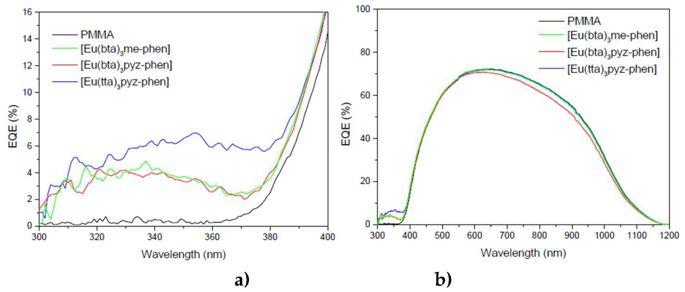
Luminescent down-shifting (LDS) layers containing the complex C4, C5 and C6 embedded in polymethylmethacrylate (PMMA) have been placed on top of the mini module used to study their photovoltaic conversions compared to the PMMA when there is not complex.
Figure 16 a) shows a positive increase in
EQE values for the 300–400 nm spectral region and
Figure 16 b) shows the EQE values for the 300–1200 nm spectral region.
The
EQE measurements shown in
Figure 16 b) show that the complexes C5 and C6 used as DS layers (blue and green lines) can improve the efficiency as we show in next sections.
3.6.4. DS layers encapsulated using C6 and C12-17 complexes
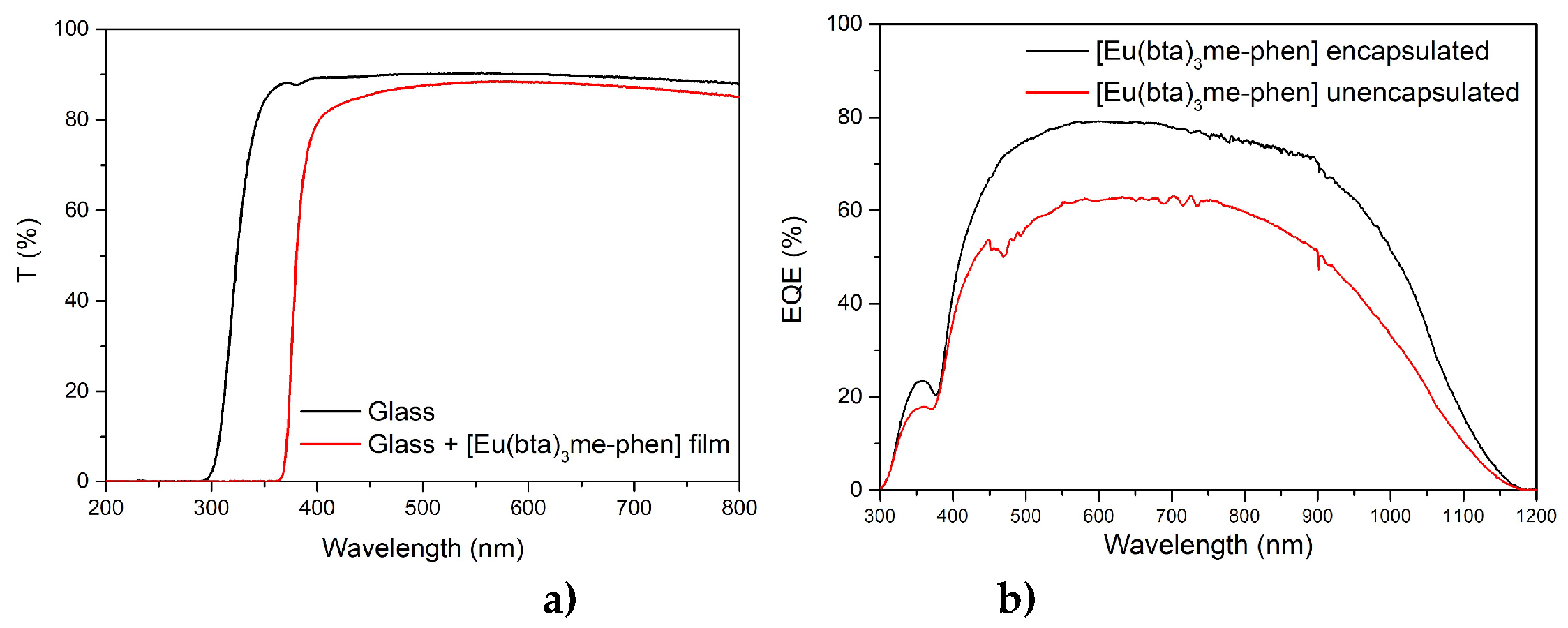
First, the DS films were just put on top of the PV devices without any encapsulation process, obtaining an increase of the EQE for the 310 – 370 nm spectral range. However, in the region of the solar spectrum where the mini-modules have a good response (380–1100 nm) the DS films reduce their efficiency due to poor transmittance, which indicates that the encapsulation of the films on top of the PV devices was necessary.
In the beginning, the films were made with PMMA as mentioned before, but it wasn’t possible to obtain clear and homogenous luminescent DS films after the encapsulation process. EVA is the main encapsulant polymer used in the fabrication process of PV devices, so we tried doing the films with it. Clear DS films that enhanced the
EQE of the mini-modules for the 300–370 nm range were obtained using EVA (
Figure 17 b)). These films also eliminated any losses between 380 nm and 1100 nm thanks to a greater transmittance. In addition, encapsulating the films prevents contact between the DS complex and atmospheric dioxygen. This results in increased efficiency of the down-shifting process by avoiding non-radiative deactivation of the excited states of the ligands due to interference from the triplet state of the dioxygen molecule. Therefore, the
EQE response in the UV region of the spectrum is higher after encapsulation.
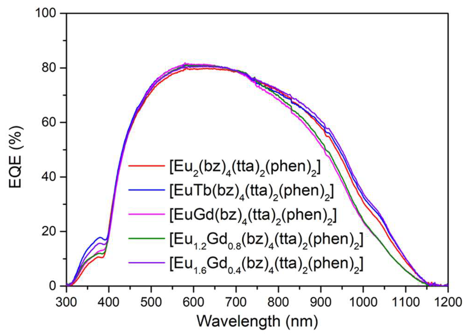
Once the conditions of the films and the encapsulation process were optimized, the
EQE measurements of all complexes encapsulated on top of the mini-module were performed (
Figure 18). The greatest increase in
EQE was observed in the heterobimetallic compounds C14 and C17, with increases of 16.3% and 14.3%, respectively, for the 300 – 400 nm spectral range. These compounds were found to exhibit high quantum yields in the photoluminescence study. In the case of the C6 complex, there was a 10.0% increase in
EQE under the same conditions. The C6 complex was subjected to a UV aging process, as explained in the next section.
Table 6 shows that all encapsulated LDS layers resulted in a significant increase in both
EQE and
Jsc within the 300–400 nm spectral range. The highest values were observed for samples C6, C14, and C17 when they were encapsulated in the mini module. These three complexes have positively contributed to the increase in the relative percentage of conversion efficiency within the 300–1200 nm spectral range.
In
Table 6, we also wanted to show
Jsc results through new experiments conducted with intensity-voltage (IV) curves measurements using a solar simulator AM1.5G, using reflectors. The increase in efficiency of the mini-module used for C12-17 complexes was obtained when a hemispherical reflector (concentrator) on top of the downshifter is placed. We have achieved, in the best case scenario for the DS layer with complex C14 an increase in conversion efficiency of 0.52% using a PV mini-module of 12.1% of efficiency [
31].
3.6.5. Accelerate aging of DS layers encapsulated using complex C6
Cycles of UV radiation were applied to samples of C6 complex for varying durations: 2, 5, 10, 50, and 100 hours, totaling 2000 hours of exposure. Two samples of [Eu(bta)
3me-phen] encapsulated on top of a mini-module were used, featuring two different film configurations of complex C6 on the glass surface (face-up, FU, and face-down, FD). These samples underwent a study to assess degradation caused by UV radiation within a climatic chamber. In
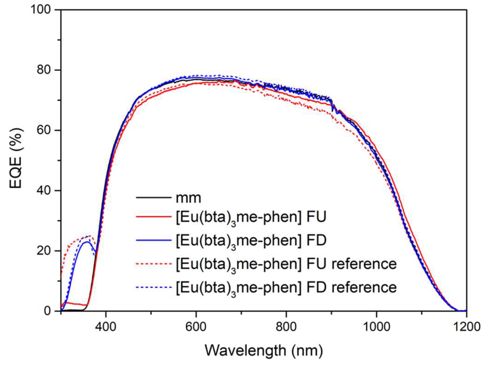
Figure 19, the
EQE curves of the reference samples (non-degraded, without UV exposure) and the study samples after exposure to 450 kW/m2 of UV radiation (2000 hours in the climatic chamber) are presented. At the end of the study, the FU sample contributes only up to 2.5% to the
EQE for the 300-400 nm spectral region. In contrast, the DS-FD sample exhibits a contribution above 20% at a wavelength of 350 nm compared to the reference sample without the down-shifting complex after 2000 hours.
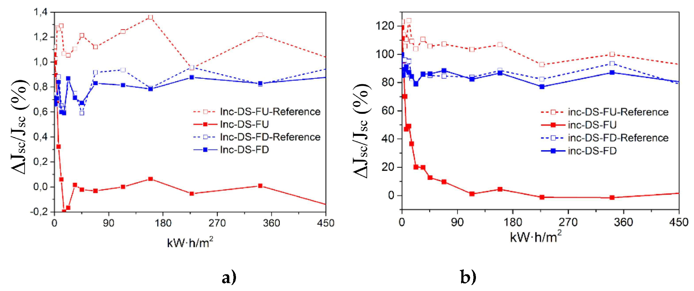
Figure 20 a) shows a remarkable relative increase in percentage of efficiency, (𝛥𝜂/𝜂) (%), when the DS layer encapsulated is not subject to UV degradation for the configuration DS-FU sample around 1.2% for the 300–1200 spectral range, and 120% for the 300–400 spectral range as we show in
Figure 20 b).
After 600 hours of UV radiation exposure, the DS-FU sample shows no significant relative increase in efficiency. On the other hand, the DS-FD sample demonstrates minimal UV degradation, with a relative increase in efficiency (Δη/η) exceeding 80% for the 300-400 nm spectral range and approximately 0.8% for the 300-1200 nm spectral range.
3.6.6. Application of complex C6 to a bifacial solar cell
In this section, we want to report initial studies conducted with bifacial mini-modules using one of the most studied complexes from the previous sections, C6. In future work, we are already considering other complexes for evaluation. We used two bifacial solar cells from CENER (National Renewable Energy Centre) in Navarra, Spain. In one of the bifacial mini modules (first experiment), we conducted a series of measurements when the C6 complex is directly deposited on top of the mini module by dissolving it in tetrahydrofuran (THF). 300 microliters of the compound are deposited using a micropipette via drop casting (DS film). In another bifacial mini module (second experiment), we encapsulated the compound deposited on glass with EVA (DS layer). In all cases, we performed an experimental setup where the light is incident perpendicularly on both sides.
3.6.6.1. First experiment
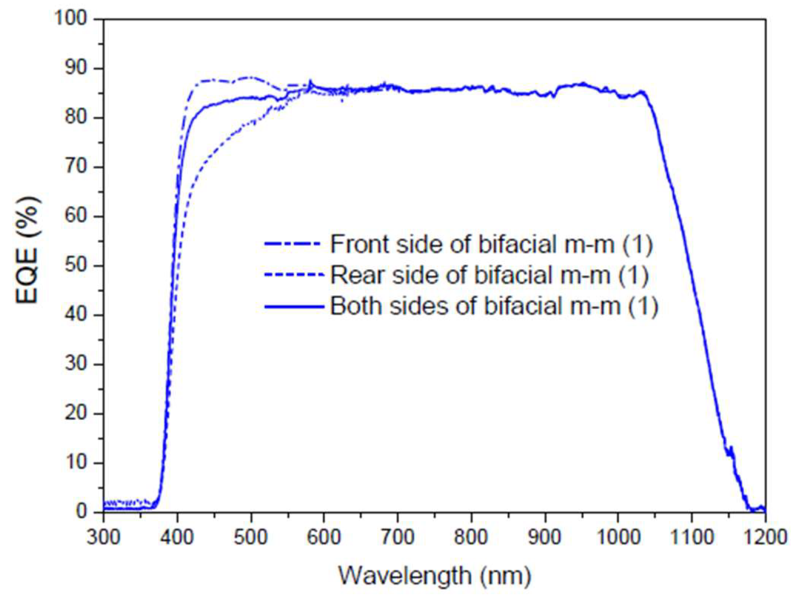
Figure 21 shows the measurements taken in a first experiment to obtain the
EQE values of a multicrystalline silicon bifacial mini module in the spectral range of 300 to 1200 nm. The
EQE dependence was obtained for the wavelength on the front side, the rear side, and for both sides. The total
EQE (illumination from both sides) is not the sum of the individual
EQEs (illumination from each side); it is the sum of the
EQEs of each side weighted by a factor that depends on the percentage of illumination from each side, where the sum of those factors is the total incident light.
The evaluation of current density was performed using
EQE measurements, and we calculated a parameter called the bifaciality factor,
BF (%), which is defined as the ratio between the value of
Jsc when illuminated from rear side and its value when illuminated solely from the other side [
72].
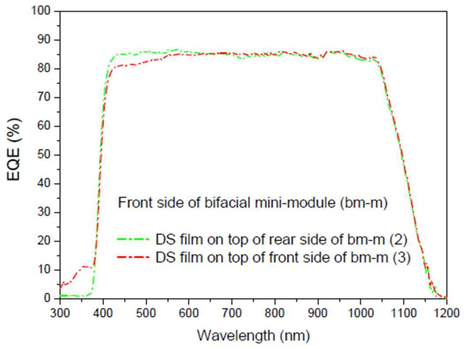
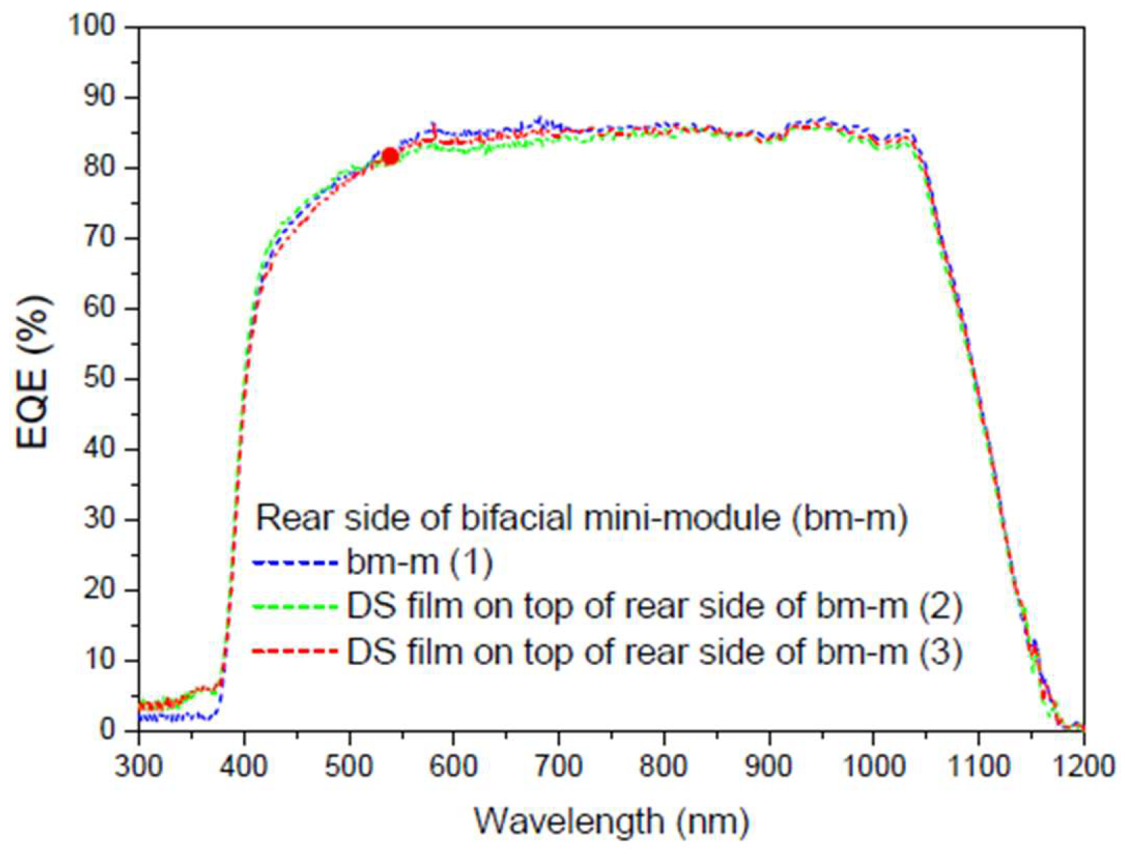
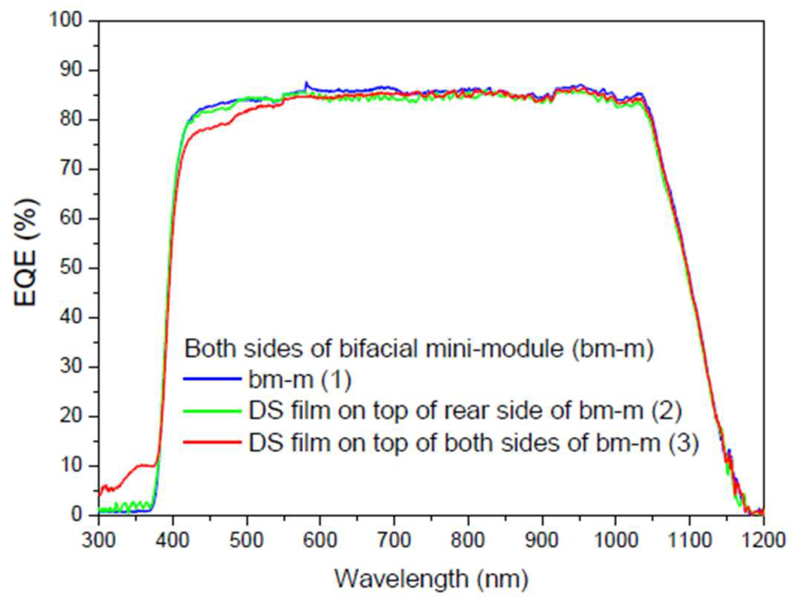
Table 7 presents these calculations for all
EQE measurements conducted (
Figure 22 and
Figure 23).
As the
EQE cannot be used to assess current values with illumination from both sides of the bifacial cell (
Figure 24), the main conclusion here is that, in addition to achieving an increase in the bifaciality factor when the film is placed on the rear side (+20.6%) in the UV-Vis range, there is an overall increase in the bifaciality factor across the entire spectral range when films are placed on both sides (0.76%), even though some loss occurs in the UV-Vis range. These conditions are considered non-field working conditions. Different incidences should be studied in future works.
3.6.6.2. Second experiment
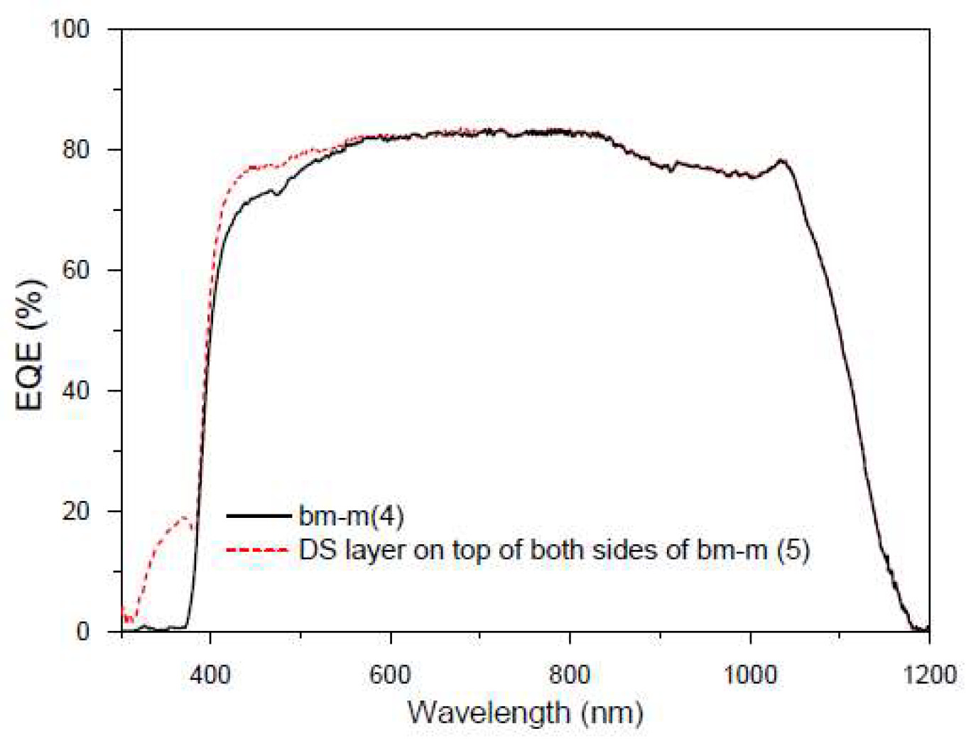
In this second experiment, we have encapsulated the compound used in the first experiment with EVA on another bifacial mini module. We present preliminary
EQE results in
Figure 25, measuring with normal incidence from both sides simultaneously, bm-m(4), and repeating the measurement when the DS layer is encapsulated on both sides, bm-m(5).
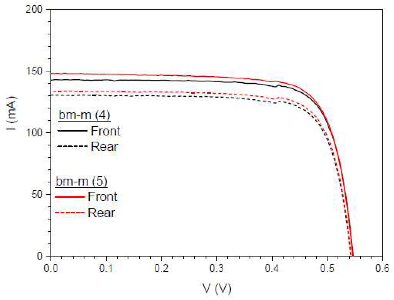
Once the increase in EQE obtained by encapsulating the DS film onto the mini module is observed, we have decided to conduct some experiments measuring the IV curves as detailed below. As mentioned earlier, it is not possible to extract a current value from the EQE measurement with illumination from both sides, as it would be a linear combination of the currents measured on each side rather than their sum.
In
Figure 26, we present IV measurements with 1 Sun illumination first on the front side and then on the rear side, considering an effective area of 4 cm
2.
Table 8.
Calculated values of the short circuit current Isc , bifaciality factor BF , maximum power Pmax, and the efficiency 𝜂 for one Sun of illumination and 4 cm2 of area.
Table 8.
Calculated values of the short circuit current Isc , bifaciality factor BF , maximum power Pmax, and the efficiency 𝜂 for one Sun of illumination and 4 cm2 of area.
| Device |
Isc (mA) Front
|
Isc (mA) Rear |
BF(%) |
Pmax (mW) Front |
Pmax (mW) Rear |
η(%)
Front
|
η(%)
Rear
|
| bm-m(4) |
142.96 |
130.58 |
91.34 |
60.22 |
54.37 |
15.05 |
13.59 |
| bm-m(5) |
148.18 |
133.80 |
90.29 |
61.39 |
55.66 |
15.35 |
13.91 |
We also calculated another parameter called the separation rate,
SR(%) , which is defined to quantitatively assess the difference between the sum of
Jsc when illuminated from each side of the bifacial cell and
Jsc when illuminated simultaneously from both sides [
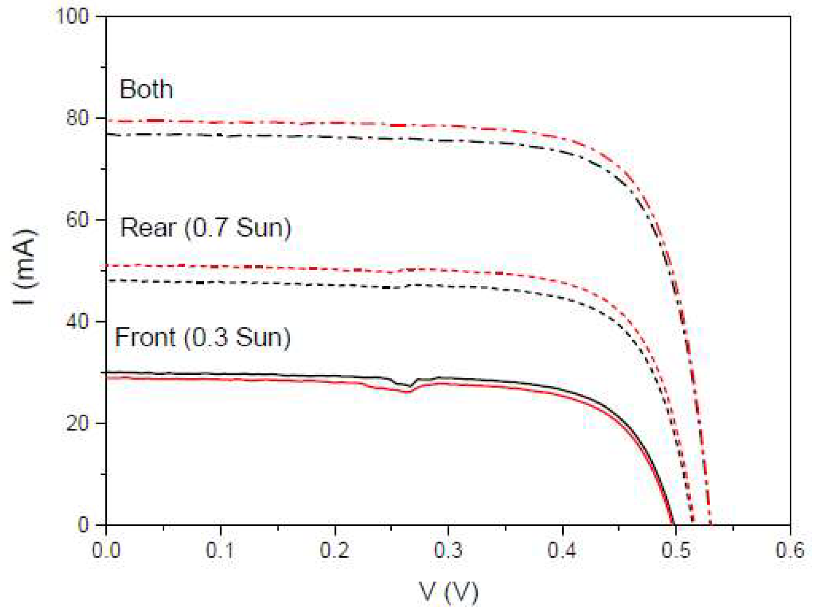
73]. We have studied the separation rate in a more realistic situation where the fraction of incident light from the one side of the bifacial cell is lower than in the other side. In
Figure 27, we present IV measurements with an illumination of 0.3 Sun on the rear side and 0.3 Sun on the front side.
Table 9.
Calculated values of the short circuit current Isc , the separate rate SR, and the maximum power Pmax, for 0.3 and 0.7 Sun of illuminations on front and rear sides, respectively, and 4 cm2 of area.
Table 9.
Calculated values of the short circuit current Isc , the separate rate SR, and the maximum power Pmax, for 0.3 and 0.7 Sun of illuminations on front and rear sides, respectively, and 4 cm2 of area.
| Device |
Isc (mA) Front |
Isc (mA) Rear |
Isc (mA) Both |
SR (%) |
Pmax (mW) Front |
Pmax (mW) Rear |
Pmax (mW) Both |
| bm-m(4) |
30.04 |
48.09 |
76.85 |
-1.6 |
10.66 |
18.20 |
30.66 |
| bm-m(5) |
28.95 |
51.13 |
79.53 |
-0.7 |
10.16 |
19.46 |
31.77 |
Just as the bifaciality factor gives the percentage of photogenerated current between the rear and front of the mini-module, the separate rate give us the percentage of current that separates the measured current when both sides are illuminated, from the sum of the photogenerated currents by the front and rear sides of the mini-module.
4. Conclusions
This work presents the results of our most recent research on the synthesis, characterization and stability of luminescent complexes as downshifters for their application in improving the efficiency of photovoltaic solar cells. The results and applications of three series of photoluminescent complexes as downshifters are shown.
In the first series, the strengths of complexes C1–3, and C6 as downshifters are summarized, and new complexes C4 and C5 were characterized as potential candidates as well. First studies of C1 and C2 complexes to create DS layers were carried out and an increase in efficiency conversion of 0.1% was obtained. DS layers were studied for different concentrations of the complex C3, where around 30% was the limit of concentration. For the PV mini module based on a single p-type mc-Si solar cell with a 16% conversion efficiency, the increases were 0.17% and 0.31%, for 10% and 30% concentrations of complex C3, respectively. The increase was 0.46% for 30% of concentration of C3 when a hemispherical reflector (concentrator) on top of the downshifter is placed.
Different experimental configurations of the DS layers of complex C6 encapsulated were studied when they were exposed to UV aging to find the optimal configuration.
In the second series, possible applications of complexes C7–11 are highlighted through their photoluminescent characterization, and although they were not studied as DS layers, they are candidates to future works. The intense emission exhibited by the Er(III) and Yb(III) complexes suggests their potential applications in optical amplifiers and bio-imaging.
We highlight the effectiveness of compounds C12-17 as downshifters in our recent investigations, particularly when utilizing bridging ligands like benzoate to form hetero-dinuclear complexes. These films can be applied to encapsulate a photovoltaic multi-crystalline silicon mini-module, resulting in improved efficiency through the down-shifting process for all the compounds within the 300-400 nm range. Additionally, the DS layers of complexes C14 and C17 demonstrate enhanced performance across the 300-1200 nm spectral range.
We have also applied the C6 complex for the use of DS layers in a bifacial cell, obtaining preliminary results that may be interesting for these types of devices.
Figure 1.
Schematic representation of photophysical processes in lanthanide (III) complexes (antenna effect). Abbreviations: A = absorption; F = fluorescence; P = phosphorescence; L = lanthanide-centered luminescence; ISC = intersystem crossing; ET = energy transfer; S = singlet; T
1 = triplet. Full vertical lines indicate radiative transitions; dotted vertical lines indicate nonradiative transitions. Reprinted with permission from [
19]. Copyright 2009 American Chemical Society.
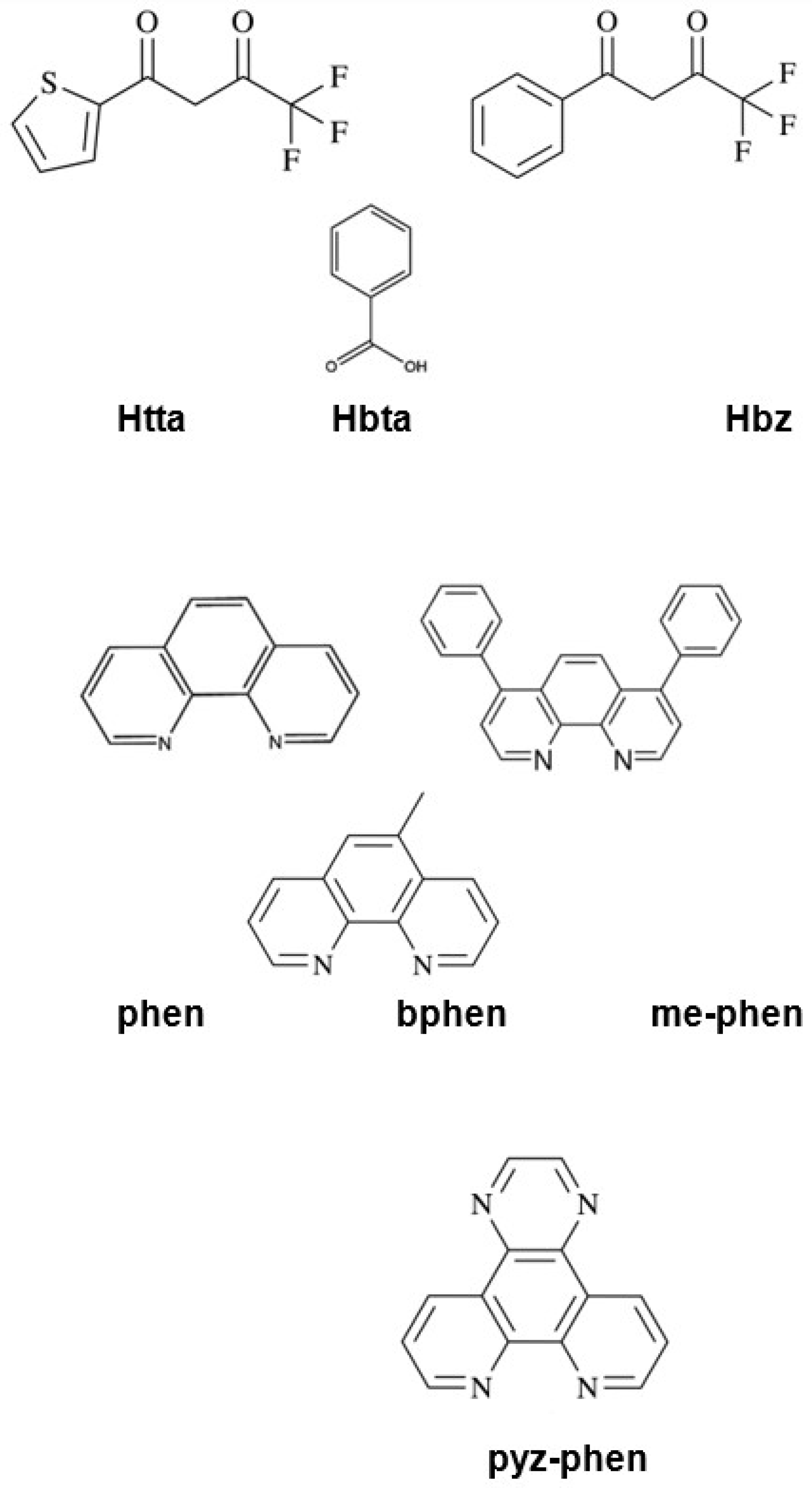
Scheme 1.
Structure of thenoyltrifluoroacetone (Htta), 1-benzoyl-3,3,3-trifluoroacetone (Hbta), benzoic acid (Hbz), phenanthroline (phen), 4,7-biphenyl-1,10-phenanthroline (bphen), 5-methyl-1,10-phenanthroline (me-phen) and pyrazino[2,3-f][1,10]phenanthroline (pyz-phen) ligands.
Scheme 1.
Structure of thenoyltrifluoroacetone (Htta), 1-benzoyl-3,3,3-trifluoroacetone (Hbta), benzoic acid (Hbz), phenanthroline (phen), 4,7-biphenyl-1,10-phenanthroline (bphen), 5-methyl-1,10-phenanthroline (me-phen) and pyrazino[2,3-f][1,10]phenanthroline (pyz-phen) ligands.
Figure 3.
UV-vis spectra of C1 and C2 complexes: [Eu2(phen)2(bz)6] and [Eu2(bphen)2(bz)6] in CH2Cl2 at c ≈ 2.5 x 10⁻⁶ M.
Figure 3.
UV-vis spectra of C1 and C2 complexes: [Eu2(phen)2(bz)6] and [Eu2(bphen)2(bz)6] in CH2Cl2 at c ≈ 2.5 x 10⁻⁶ M.
Figure 4.
UV-vis absorption spectra of the Hbta, Htta, bphen, me-phen and pyz-phen ligands together with [Eu(tta)3bphen] (C3), [Eu(bta)3pyz-phen] (C4), [Eu(tta)3pyz-phen] (C5), and [Eu(bta)3me-phen] (C6) complexes in ethanol at c ≈ 10-5 M.
Figure 4.
UV-vis absorption spectra of the Hbta, Htta, bphen, me-phen and pyz-phen ligands together with [Eu(tta)3bphen] (C3), [Eu(bta)3pyz-phen] (C4), [Eu(tta)3pyz-phen] (C5), and [Eu(bta)3me-phen] (C6) complexes in ethanol at c ≈ 10-5 M.
Figure 5.
UV-vis absorption spectra of the Hbta, Htta, me-phen and pyz-phen ligands together with Yb(III) and Er(III) complexes in ethanol at c ≈ 10-5 M.
Figure 5.
UV-vis absorption spectra of the Hbta, Htta, me-phen and pyz-phen ligands together with Yb(III) and Er(III) complexes in ethanol at c ≈ 10-5 M.
Figure 6.
UV-vis absorption spectra of the Hbz, Htta, and phen ligands together with [M1M2(bz)4(tta)2(phen)2] complexes in ethanol at c ≈ 10-5 M.
Figure 6.
UV-vis absorption spectra of the Hbz, Htta, and phen ligands together with [M1M2(bz)4(tta)2(phen)2] complexes in ethanol at c ≈ 10-5 M.
Figure 7.
a) Antenna excitation between 250 and 400 nm and b) corresponding Eu3+ emission spectra of C2 at 5% (red line) and 10%(blue line) in PMMA.
Figure 7.
a) Antenna excitation between 250 and 400 nm and b) corresponding Eu3+ emission spectra of C2 at 5% (red line) and 10%(blue line) in PMMA.
Figure 8.
Emission spectra of C3-6 complexes obtained under excitation with a xenon lamp at 350 nm.
Figure 8.
Emission spectra of C3-6 complexes obtained under excitation with a xenon lamp at 350 nm.
Figure 9.
Emission spectra of [Eu(bta)3me-phen] and all [M1M2(bz)4(tta)2(phen)2] containing Eu(III) ion obtained under excitation with a xenon lamp at 350 nm.
Figure 9.
Emission spectra of [Eu(bta)3me-phen] and all [M1M2(bz)4(tta)2(phen)2] containing Eu(III) ion obtained under excitation with a xenon lamp at 350 nm.
Figure 10.
Emission spectra of a) [Yb(bta)3me-phen] and [Yb(bta)3pyz-phen] and b) [Er(bta)3me-phen] and [Er(tta)3pyz-phen] exciting with a 375 nm laser.
Figure 10.
Emission spectra of a) [Yb(bta)3me-phen] and [Yb(bta)3pyz-phen] and b) [Er(bta)3me-phen] and [Er(tta)3pyz-phen] exciting with a 375 nm laser.
Figure 11.
Emission spectra of a) [Gd(bta)3me-phen] exciting with a 375 nm laser and b) [Gd2(bz)4(tta)2(phen)2] exciting with a xenon lamp at 350 nm.
Figure 11.
Emission spectra of a) [Gd(bta)3me-phen] exciting with a 375 nm laser and b) [Gd2(bz)4(tta)2(phen)2] exciting with a xenon lamp at 350 nm.
Figure 12.
EQE values ranging between 0 and 1 were obtained for the 280–350 nm spectral range for various experimental configurations of the DS layer of complex C1 placed on the reference cell (RC). a) The EQE behavior was analyzed when the DS layer was deposited through spin coating or tape casting on glass and b) Additionally, the EQE behavior was studied when the DS layer was deposited through tape casting on the rear side of the glass and covered by a UV reflector.
Figure 13.
a) EQE values in percentage were measured for the 280 – 350 nm spectral range and b) for 280 – 1200 nm spectral range when the reference solar cell (RSC) is covered with the clean glass (black dashed line) and with 5% (red line) and 10% (blue line) of C3 complex.
Figure 13.
a) EQE values in percentage were measured for the 280 – 350 nm spectral range and b) for 280 – 1200 nm spectral range when the reference solar cell (RSC) is covered with the clean glass (black dashed line) and with 5% (red line) and 10% (blue line) of C3 complex.
Figure 14.
EQE values in percentage for the 280 – 400 nm spectral range were measured for different concentrations (ranging from 1% to 30%) of complex C3 embedded in a thin PMMA film of the DS layer. The film was deposited on a glass substrate (G) and placed on the PV mini-module (M).
Figure 14.
EQE values in percentage for the 280 – 400 nm spectral range were measured for different concentrations (ranging from 1% to 30%) of complex C3 embedded in a thin PMMA film of the DS layer. The film was deposited on a glass substrate (G) and placed on the PV mini-module (M).
Figure 15.
a) EQE values, expressed as a percentage, were measured for the spectral range of 280–1200 nm using a 30% concentration of the C3 complex in the down converter (DC) layer following the experimental configuration for the values obtained in
Figure 14.
b) Additionally, the EQE values were measured when the DC layer was covered by a hemispherical reflector (concentrator).
Figure 16.
a) EQE values in percentage for the 300 – 400 nm spectral range and b) for the 300 – 1200 nm spectral range were measured for the DS layers of C4-6 complexes.
Figure 16.
a) EQE values in percentage for the 300 – 400 nm spectral range and b) for the 300 – 1200 nm spectral range were measured for the DS layers of C4-6 complexes.
Figure 17.
a) Transmittance (T) values in percentage for the UV-vis spectral range of the bare glass (black line) and C6 complex embedded in EVA and deposited on the glass (red line) and b) EQE values in percentage for the 300–1200 nm spectral range were measured for the DS layer of C6 complex before and after encapsulating.
Figure 18.
EQE values in percentage of the mini-modules with the DS layers of [M1M2(bz)4(tta)2(phen)2] complexes containing Eu(III) ions encapsulated on top of them.
Figure 18.
EQE values in percentage of the mini-modules with the DS layers of [M1M2(bz)4(tta)2(phen)2] complexes containing Eu(III) ions encapsulated on top of them.
Figure 19.
The EQE response of the encapsulated samples was evaluated after a 2000-hour exposure to the xenon lamp within the climatic chamber, covering the spectral range of 300-1200 nm. The dashed lines represent the measurements taken before any UV aging, while the solid lines depict the EQE behavior after exposure to UV radiation.
Figure 20.
a) The evolution in relative increase in percentage of current density, ΔJsc /Jsc (%), after exposure to UV radiation (kWh/m2) (solid lines) compared to those without undergoing UV aging (dashed lines), for the 300–120 spectral range and b) for 300–400 nm spectral range.
Figure 20.
a) The evolution in relative increase in percentage of current density, ΔJsc /Jsc (%), after exposure to UV radiation (kWh/m2) (solid lines) compared to those without undergoing UV aging (dashed lines), for the 300–120 spectral range and b) for 300–400 nm spectral range.
Figure 21.
EQE values in percentage of a bifacial mini-module, bm-m(1), when illuminated on the front (dash dot line) , rear (short dash line) , and both sides (blue solid line) in the range from 300 to 1200 nm.
Figure 21.
EQE values in percentage of a bifacial mini-module, bm-m(1), when illuminated on the front (dash dot line) , rear (short dash line) , and both sides (blue solid line) in the range from 300 to 1200 nm.
Figure 22.
EQE values in percentage of the bifacial mini-module with down shifter films of complex C6 on top of the rear side (green line), bm-m(2), and both sides (red line), bm-m(3), when illuminated on the front side in the range from 300 to 1200 nm.
Figure 22.
EQE values in percentage of the bifacial mini-module with down shifter films of complex C6 on top of the rear side (green line), bm-m(2), and both sides (red line), bm-m(3), when illuminated on the front side in the range from 300 to 1200 nm.
Figure 23.
EQE values in percentage of the bifacial mini-module with down shifter films of complex C6 on top of the rear side(green line) , bm-m (2), and both sides (red line), bm-m(3), when illuminated on the rear side in the range from 300 to 1200 nm.
Figure 23.
EQE values in percentage of the bifacial mini-module with down shifter films of complex C6 on top of the rear side(green line) , bm-m (2), and both sides (red line), bm-m(3), when illuminated on the rear side in the range from 300 to 1200 nm.
Figure 24.
EQE values in percentage of the bifacial mini-module with down shifter films of complex C6 on top of the rear side(green line) , bm-m (2), and both sides (red line), bm-m(3), when illuminated on both sides in the range from 300 to 1200 nm.
Figure 24.
EQE values in percentage of the bifacial mini-module with down shifter films of complex C6 on top of the rear side(green line) , bm-m (2), and both sides (red line), bm-m(3), when illuminated on both sides in the range from 300 to 1200 nm.
Figure 25.
EQE values in percentage of the bifacial mini-module bm-m(4) (black line), and when a DS layer of complex C6 is encapsulated on both sides bm-m(5) (red line) when illuminated on both sides in the range from 300 to 1200 nm.
Figure 25.
EQE values in percentage of the bifacial mini-module bm-m(4) (black line), and when a DS layer of complex C6 is encapsulated on both sides bm-m(5) (red line) when illuminated on both sides in the range from 300 to 1200 nm.
Figure 26.
IV curves of the bifacial mini-module, bm-m(4) (black line), and when a DS layer of complex C6 is encapsulated on both sides, bm-m(5) (red line), when illuminated on front side (solid lines) and rear side (red lines), all under one Sun of illumination.
Figure 26.
IV curves of the bifacial mini-module, bm-m(4) (black line), and when a DS layer of complex C6 is encapsulated on both sides, bm-m(5) (red line), when illuminated on front side (solid lines) and rear side (red lines), all under one Sun of illumination.
Figure 27.
IV curves of the bifacial mini-module, bm-m(4) (black line), and when a DS layer of complex C6 is encapsulated on both sides, bm-m(5) (red line), when illuminated on front side under 0.3 Sun of illumination (solid lines), on rear side under 0.7 Sun of illumination (short dash lines), and on both sides of illumination (dash dot lines).
Table 1.
Molecular structures of the C1–6 complexes.
Table 2.
Coordination environment of Yb(III) and Er(III) and molecular structures of the C7–11 complexes.
Table 4.
Lifetime (τ) and PLQY of the complexes.
Table 4.
Lifetime (τ) and PLQY of the complexes.
| Complex |
λexc (nm) |
λem (nm) |
τ (ms) |
PLQY (%) |
Reference |
| C1 |
340 |
614 |
1.02 |
48 |
[23] |
| C2 |
280 |
0.96 |
50 |
this work, [69] |
| C3 |
340 |
612 |
0.98 |
69 |
this work, [24,70] |
| C4 |
375 |
0.53 |
|
this work |
| C5 |
375 |
0.81 |
|
| C6 |
350 |
0.54 |
|
| C7 |
375 |
1550 |
1.6 10-3
|
|
this work, [30] |
| C8 |
980 |
7.2 10-3
|
|
| C10 |
980 |
6.1 10-3
|
|
| C11 |
1550 |
1.3 10-3
|
|
| C12 |
350 |
612 |
0.60 |
63 |
this work, [31] |
| C14 |
0.75 |
66 |
| C15 |
0.65 |
50 |
| C16 |
0.72 |
70 |
| C17 |
0.74 |
74 |
Table 5.
Calculated values of the increment in relative percentage of conversion efficiency, (Δη/η) % for C1 complex at 2% of concentration.
Table 5.
Calculated values of the increment in relative percentage of conversion efficiency, (Δη/η) % for C1 complex at 2% of concentration.
| Complex used |
(Δη/η) (%) (285-350 nm)
|
(Δη/η) (%) (285-1200 nm)
|
| C1 (tape casted) |
279.0 |
0.1 |
| C1 (spin coated) |
143.0 |
< 0.1 |
| C1 (tape casted and reflector) |
347.0 |
0.18 |
Table 6.
Increase in percentages of EQE values at 370 nm (ΔEQE), Jsc values for the 300 – 1200 nm spectral range, and the 300 – 400 nm spectral range of the mini module (m-m) with the DS layers encapsulated, as well as their increments (ΔJsc) compared to the m-m for the 300 – 1200 nm spectral range, and the 300 – 400 nm spectral range when there is no complex. The estimates for the increase in relative percentage of conversion efficiency (Δη/η) % compared to the m-m when there is no complex are also displayed.
| Complex |
ΔEQE (%) a
|
Jsc (mA/cm2) b |
ΔJsc (mA/cm2) b |
(Δη/η) ( %)b
|
Jsc (mA/cm2) c
|
ΔJsc (mA/cm2) c
|
(Δη/η) ( %) c
|
| m-m used for C6 |
— |
28.40 |
|
|
0.18 |
— |
|
| C6 |
10.0 |
28.70 |
0.30 |
1.05 |
0.29 |
0.11 |
61.1 |
| m-m used for C12–17 |
— |
d
25.80 |
e
26.86 |
|
|
0.05 |
— |
|
| C12 |
9.7 |
25.53 |
26.46 |
— |
— |
0.13 |
0.08 |
160 |
| C13 |
11.4 |
24.79 |
25.60 |
— |
— |
0.15 |
0.10 |
200 |
| C14 |
16.3 |
26.69 |
26.95 |
0.89; 0.09 |
3.45; 0.33 |
0.20 |
0.15 |
300 |
| C16 |
10.9 |
25.40 |
25.78 |
— |
— |
0.14 |
0.09 |
180 |
| C17 |
14.3 |
26.04 |
27.04 |
0.24; 0.18 |
0.93; 0.67 |
0.17 |
0.12 |
240 |
Table 7.
Calculated values of the current density, Jsc, and bifaciality factor, BF for (a) 300-1200 nm and (b) 300-400 nm spectral ranges.
Table 7.
Calculated values of the current density, Jsc, and bifaciality factor, BF for (a) 300-1200 nm and (b) 300-400 nm spectral ranges.
| Device |
Jsc (mA/cm2) Front |
Jsc (mA/cm2) Rear |
Bifaciality Factor (%) |
| (a) bm-m(1) |
36.18 |
35.15 |
97.15 |
| (b) bm-m(1) |
19.00 |
14.49 |
76.26 |
| (a) bm-m(2) |
35.71 |
34.69 |
97.14 |
| (b) bm-m(2) |
19.56 |
17.99 |
91.97 |
| (a) bm-m(3) |
35.60 |
34.85 |
97.89 |
| (b) bm-m(3) |
25.04 |
17.16 |
68.53 |
