
Submitted:
19 June 2023
Posted:
20 June 2023
You are already at the latest version
Abstract
This paper presents a 32 GHz high power amplifier (HPA) with a design strategy to achieve a high-power output with reliable operation for the Ka-band deep space satellite communication in 150 nm GaN HEMT technology. The presented Ka-band HPA employs a cascaded two-stage common source amplifier topology, and the output stage is comprised of an 8-way power combining network in current mode. The interstage matching network is designed with the bandpass configuration utilizing capacitors and transmission lines to provide better stability at the low-frequency regime. The implemented Ka-band HPA achieved a peak power gain of 7.3 dB at 32 GHz and a 3 dB bandwidth was 3.5 GHz between 31.3 and 34.8 GHz. The saturated output power at the peak power added efficiency (PAE) of 19.3% was 38.2 dBm, and the output 1 dB gain compression point (OP1dB) was 27.4 dBm in the measurement. The designed HPA consumes an area of 19.35 mm^2 including RF signal, and DC pads
Keywords:
mm-wave
; deep space exploration
; satellite communication
; power amplifier
; GaN
; HEMT
1. Introduction
Deep space exploration has been developed since the 1960s, and unmanned probes are exploring the far reaches of outer space and transferring data back to Earth. Early data transfers for deep space exploration were sufficient with a few kbps, but the demand for higher data rates has grown over time. It is essential to provide a large amount of communication capacity on spacecraft-to-Earth links to achieve this aim. As a result, deep space radio communication systems have moved toward higher frequencies, from L-band to S-band which was followed by S-band to X-band [1]. Moreover, the exponentially rising amount of investigated data and the need for higher transmission capacity are driving satellite communications to higher bands, such as those above the X band [2].
Millimeter-wave frequency band allows the deep-space satellite communication systems to reach high data transmission rates, with low communication delays. The Ka-band (27-40GHz) provides relatively wide bandwidth and high throughput. The ITU radio regulations assigned the downlink frequency ranges for the deep space exploration to X-band around 8.4GHz (8.4-8.45GHz) and Ka-band around 32GHz (31.8-32.3GHz). The Ka-band downlink deep space exploration systems can downlink data at a rate approximately six times higher than X-band [3]. However, because of the Earth’s troposphere, radio meteorological factors, convective rainfall, nonprecipitating clouds, stratiform rain events, atmospheric noise temperature, and other conditions, the attenuation might be much higher at Ka-band [4]. Since signal attenuation increases during propagation at high frequency, high-performance amplifiers in the system are vital in improving the link distance and the quality of communication [5].
To develop such a high-performance transceiver at millimeter-wave regime, high-power, low-cost, and highly reliable solutions for solid-state power amplifiers have been investigated in III-V compound semiconductor technologies like gallium arsenide (GaAs), gallium nitride (GaN). The III-V compound semiconductor technology has excellent transistor characteristics in the high-frequency range, and the semi-insulating substrate facilitates high-quality integrated passive components with low parasitic elements [6]. Specifically, GaN has a high breakdown voltage from a wide energy gap of 3.4eV, high carrier concentration, high electron mobility, and high saturation velocity. Because a high breakdown voltage transistor (HEMT) is available with a high current density in GaN technology, the PA can achieve a higher output power with improved power-added efficiency (PAE) at the millimeter-wave regime. This work presents a 32GHz high power amplifier (HPA) for a deep-space satellite communication system.
2. 32-GHz High Power Amplifier Design
The designed 32GHz 8-way high power amplifier (HPA) was implemented in GaN/SiC HEMT technology with a gate length of 0.15-µm. The GaN heterostructure is grown on a SiC substrate and the source-coupled field plate structure provides an improved high breakdown voltage required for high-power RF applications. The technology supports the backside via-process to provide improved thermal conductance and reduced parasitic inductance. It is noteworthy that the backside via model from the process design kit (PDK) was tailored based on the measurements for a more accurate millimeter-wave PA design. The circuit and electromagnetic simulations have been performed using Keysight ADS.
The schematic of the 32 GHz HPA is presented in Figure 1. A cascaded two-stage common source (CS) amplifier topology is used to achieve more than 15dB gain at the operating frequency. To achieve an output power higher than 38dBm, an eight-way power combining network in the current mode was employed to effectively combine the power delivered from the parallel output stages. For each parallel HEMT, R=50 Ω is connected between each gate of the transistors to avoid any undesirable odd mode oscillation issue caused by the device asymmetry in the fabrication. As the HEMT devices are operating at 25V with high DC current, double metal layers were used for the bias line to minimize undesirable voltage drop.
2.1. Device Selection and Stabilization
In this work, an 150nm GaN HEMT technology was used. There are two types of HEMT models depending on the backside via layout configuration. One is the outside back via (OSV) HEMT and the other is the internal backside via (ISV) HEMT. With the same number of gate fingers and width, the OSV HEMT layout occupies a smaller area than that of the ISV HEMT. To minimize the chip area consumption, the OSV HEMT was used despite the fact that ISV HEMT has better self-heating performance with a large number of vias on the backside. The class-AB configuration was selected to improve the power efficiency, and the device was biased to the drain supply of 25V and the gate voltage of -1.55V. The size of the HEMT used at the first stage (H1-4) was selected to be 6×50 μm and 8×50 μm HEMT was used for the final stage (H5-12). Hence, the gate width periphery ratio is 3:8 to provide sufficient driving power margin between each driving stage.
In designing a robust high-power amplifier (HPA), stable operation of the HPA is essential. In this work, a parallel RC network at the gate was employed to improve stability, especially at a low-frequency region. Since the parallel RC network at the gate of each HEMT degrades the power gain and efficiency, it is critical to determine the proper values of the resistance and capacitance of the parallel RC networks for a high-performance HPA design. To guarantee unconditional stability from 100 MHz to 50 GHz, the parallel RC network was comprised of a 40 Ω resistor and 580fF capacitor for 6x50μm and a 50Ω resistor and 630fF capacitor for 8x50μm. Figure 2 shows the simulated maximum power gain (Gma) and the μ- stability factor of the 6x50μm, and 8x50μm OSV layout devices. The Gma at 32 GHz is reduced from 13.1dB to 12dB for 6x50μm, and from 14.4dB to 11.5dB for 8x50μm. Meanwhile, the device itself is unconditionally stable with μ > 1 from 100 MHz to 50GHz. Figure 2 presents the effects of the parallel RC network on the maximum power gain (Gma) and μ-stability with and without the parallel RC network.
In combining multiple parallel HEMT devices, there is a possibility of odd-mode oscillations which can be caused by the electrical asymmetry from the differences in transconductance, biasing current, and nonlinear parasitic capacitors. It is noted that the odd-mode instability is not predictable from either μ or K-Δ stability factor from the small signal S-parameter simulations. To suppress unpredictable instability, resistors are placed between paralleled transistor branches [7].
Sufficient bypass capacitors are essential to suppress the noise, interferences, and RF leakages through the bias circuits. To improve the stability of the HPA, we added a de-Qing resistor in series with the bypass capacitor to suppress the ringing of the series RLC network from the parasitic routing inductance (Lpara). It is important to select a proper series resistance since the de-Qing resistor trades off with the performance of the filtering capacitance. To keep the series RLC network in the over-damped oscillation, the series de-Qing resistor RdeQ should meet the condition given by
,
where Lpara is the routing inductance, and Cbypass is the bypass capacitance. It is noted that Lpara should be minimized to keep RdeQ small enough not to degrade the filtering performance. The Lpara are estimated from the ADS momentum simulation and the value of Cbypass is determined to meet the over-damped oscillation condition as a function of the de-Qing resistor in time domain simulations. The parameters of the series RLC network of the bypass capacitor with de-Qing resistors are presented in Figure 3.
A simplified block diagram of implemented stabilization circuits is illustrated in Figure 4.
2.2. Impedance Matching Network Design
In designing HPA, an ADS momentum simulator is used for optimizing transmission lines for accurate impedance matching at high frequencies. The design procedure involves careful EM simulation with backside vias formed through a thick SiC substrate to avoid frequency shift and impedance mismatch. In this work, an additional backside via inductance of 32 pH was included in series with the via model from PDK. To suppress undesired low-frequency signals throughout the matching network, the matching network was designed to have a high-pass property. The output matching network determines the power delivered to the load and the power added efficiency (PAE). Load-pull simulations were used to determine the optimum output-matching impedance. A load-pull simulation of 8x50μm OSV HEMT is presented in Figure 5. The power contour step size is 0.8 dB, and the PAE contour step size is 5%. The optimum impedance for the maximum power delivery was Zpout_opt = 9.2 + j35.8 Ω and for the maximum PAE was ZPAE_opt = 4.8 + j37.5 Ω. The input impedance of the output matching network from 28GHz to 32GHz is also shown in Figure 5. To achieve a high outpower level, the output matching network has an input impedance of Zin = 12.7 + j36 Ω which is close to Zpout_opt at 32GHz.
3. Simulation and Measurement Results
The proposed 32 GHz power amplifier was designed in 150nm GaN HEMT technology with a fT of 34.5 GHz. Figure 6 shows a photograph of the implemented amplifier, which occupies an area of 4.3 mm × 4.5 mm including all the RF, ground, and DC pads. We measured the power amplifier’s S-parameters and large-signal performance. DC bias was supplied by ROHDE&SCHWARZ(R&S) HMP4040. S-parameters are measured with vector network analyzer R&S ZNB40. During large-signal measurements, the waveform generator Keysight 33250A generates a pulse-modulated signal with a 10% duty cycle and 1 ms pulse. The input signal was generated from a signal generator R&S SMA100B and for the measurement at a high input power level, a driving amplifier was used. To prevent returned signals from the reflection, an isolator Fairview Microwave FMIR1036 was used between the driving amplifier and the designed power amplifier. The output power was measured with a spectrum analyzer R&S FSV3044. The measurement setup for the S-parameter is illustrated in Figure 7. Figure 8 shows a setup for large signal measurement.
The measured small signal and large signal performances are presented in Figure 9. The gain at 32 GHz is 16.4 dB, and the 3-dB gain bandwidth was 3.5GHz between 31.3 and 34.8 GHz. The gate bias voltage was VGG = -1.55 V and the drain supply voltage was VDD = 25 V with a total drain current of 410mA. As shown in Figure 9a, the maximum gain was 16.9dB at 32.7GHz and the 3dB gain bandwidth was 3.5 GHz between 31.3 and 34.8 GHz. During the large signal test at 32 GHz under a 10% duty cycle and 1ms pulse, the Psat was measured to be 38.3 dBm (6.76 W), and the power gain was 7.3 dB. The peak PAE was 19.3% and the output of 1 dB gain compression point (OP1dB) was around 28.5 dBm. Measurement results corresponded well with the simulations with small degradations at the high-frequency regime.
Table 1 summarizes the performance of this work in comparison with the recently reported Ka-band power amplifiers. The proposed design has the best small signal gain and 3dB gain bandwidth performance compare with other 2-stage designs in Ka-band.
4. Conclusions
We presented a 2-stage 8-way 32-GHz high power amplifier (HPA) in 150nm GaN HEMT technology for Ka-band deep space satellite communication systems. To achieve a high output power with minimum chip area, outside back via (OSV) type HEMT was used with the stabilizing circuitry using a parallel RC network at the gate, and bypass capacitor network with a de-Qing resistor. The values of stabilization resistors and capacitors are selected by minimizing gain degradation. With this configuration, the whole amplifier occupies 19.35 mm2 including all the RF and DC pads. The measured amplifier demonstrated an output power of 38.3 dBm and 16. 4dB small signal gain at 32GHz with 3dB gain bandwidth of 3.5 GHz between 31.3 and 34.8 GHz which corresponds well with the simulation result.
Author Contributions
Formal analysis, data curation, H.-G.P., V.-S.T.; validation, M.-K.L., B.-H. L; data curation, M.-K.L., B.-H. L., K.-I. N.; conceptualization, formal analysis, and supervision, J.-D.P.; writing—original draft, H.-G.P.; writing—review and editing, J.-D.P. All authors have read and agreed to the published version of the manuscript.
Funding
This work was supported by the Dongguk University Research Fund of 2021 and supported by a grant-in-aid of HANWHA SYSTEMS.
Acknowledgments
This work was supported by the Dongguk University Research Fund of 2021 and supported by a grant-in-aid of HANWHA SYSTEMS.
Conflicts of Interest
The authors declare no conflict of interest. The funders had no role in the design of the study; in the collection, analyses, or interpretation of data; in the writing of the manuscript, or in the decision to publish the results.
References
- F. Davarian, S. F. Davarian, S. Shambayati, and S. Slobin, “Deep space Ka-band link management and mars reconnaissance orbiter: Long term weather statistics versus forecasting,” Proc. IEEE, vol. 92, no. 12, pp. 312–329, Nov./Dec. 2004. [CrossRef]
- Biscarini M., M. Montopoli, and F. S. Marzano, "Evaluation of HighFrequency Channels for Deep Space Data Transmission Using Radiometeorological Model Forecast", Antennas and Propagation, IEEE Transactions on, 2017, vol. 65, n. 3, pp. 1311-1320, 2017. [CrossRef]
- L. Xianfeng et al., "A Ka band transmitter for deep space communication systems," 2012 International Conference on Microwave and Millimeter Wave Technology (ICMMT), Shenzhen, China, 2012, pp. 1-3. [CrossRef]
- M. Biscarini et al., "Optimizing Data Volume Return for Ka-Band Deep Space Links Exploiting Short-Term Radiometeorological Model Forecast," in IEEE Transactions on Antennas and Propagation, vol. 64, no. 1, pp. 235-250, Jan. 2016. [CrossRef]
- Chunying Sun, Zonglin Ma, Kaixue Ma, Haipeng Fu, Xiangyang Duan, Jianli Liu, Yenan Bie; A high-linearity 24-32-GHz amplifier with AM-AM/PM compensation technology for 5G applications. IEICE Electron. Express 19(1): 20210457 (2022). [CrossRef]
- Y.-H. Yu, W.-H. Y.-H. Yu, W.-H. Hsu, and Y.-J. E. Chen, “A Ka-band low noise amplifier using forward combining technique,” IEEE Microw. Wireless Compon. Lett., vol. 20, no. 12, pp. 672–674, Dec. 2010. [CrossRef]
- R. Feghhi and M. Joodaki, “Odd-mode instability analysis of fT -doubler hybrid power amplifiers based on GaN-HEMT,” IEEE Trans. Circuits Syst. II, Exp. Briefs, vol. 68, no. 4, pp. 1193–1197, Apr. 2021. Thyagarajan, S.V.; Kang, S.; Niknejad, A.M. A 240 GHz fully integrated wideband QPSK receiver in 65 nm CMOS. IEEE J. Solid-State Circuits 2015, 50, 2268–2280.
- Y. Yamaguchi, J. Kamioka, M. Hangai, S. Shinjo, and K. Yamanaka, “A CW 20W Ka-band GaN high power MMIC amplifier with a gate pitch designed by using one-finger large signal models,” in 2017 IEEE Compound Semiconductor Integrated Circuit Symposium (CSICS), Oct 2017, pp. 1–4.
- K. Takagi, C. Y. Ng, H. Sakurai, and K. Matstushita, “GaN MMIC for Ka-Band with 18W,” in 2015 IEEE Compound Semiconductor Integrated Circuit Symposium (CSICS), Oct 2015, pp. 1–4.
- C. Y. Ng et al., “A 20-watt Ka-band GaN high power amplifier MMIC,” Microwave Conference (EuMC), 2014 44th European, 2014, pp. 1348– 1351.
- C. F. Campbell, Y. Liu, M. Y. Kao, and S. Nayak, “High efficiency Kaband Gallium Nitride power amplifier MMICs,” in 2013 IEEE International Conference on Microwaves, Communications, Antennas and Electronic Systems (COMCAS 2013), Oct 2013, pp. 1–5.
- Y. Noh, Y. Choi, I. Yom, “Ka-band GaN power amplifier MMIC chipset for satellite and 5G cellular communications,” in 2015 IEEE 4th AsiaPacific Conference on Antennas and Propagation (APCAP), June 2015. 20 June.
- S. Chen, S. S. Chen, S. Nayak, C. Campbell, and E. Reese, "High Efficiency 5W/10W 32 - 38GHz Power Amplifier MMICs Utilizing Advanced 0.15µm GaN HEMT Technology," 2016 IEEE Compound Semiconductor Integrated Circuit Symposium (CSICS), Austin, TX, USA, 2016, pp. 1-4. [CrossRef]
Figure 1.
(a) schematic of the 32GHz power amplifier (b) Parameters of the utilized components .

Figure 2.
Maximum available gain (Gma) and the μ -stability factor.
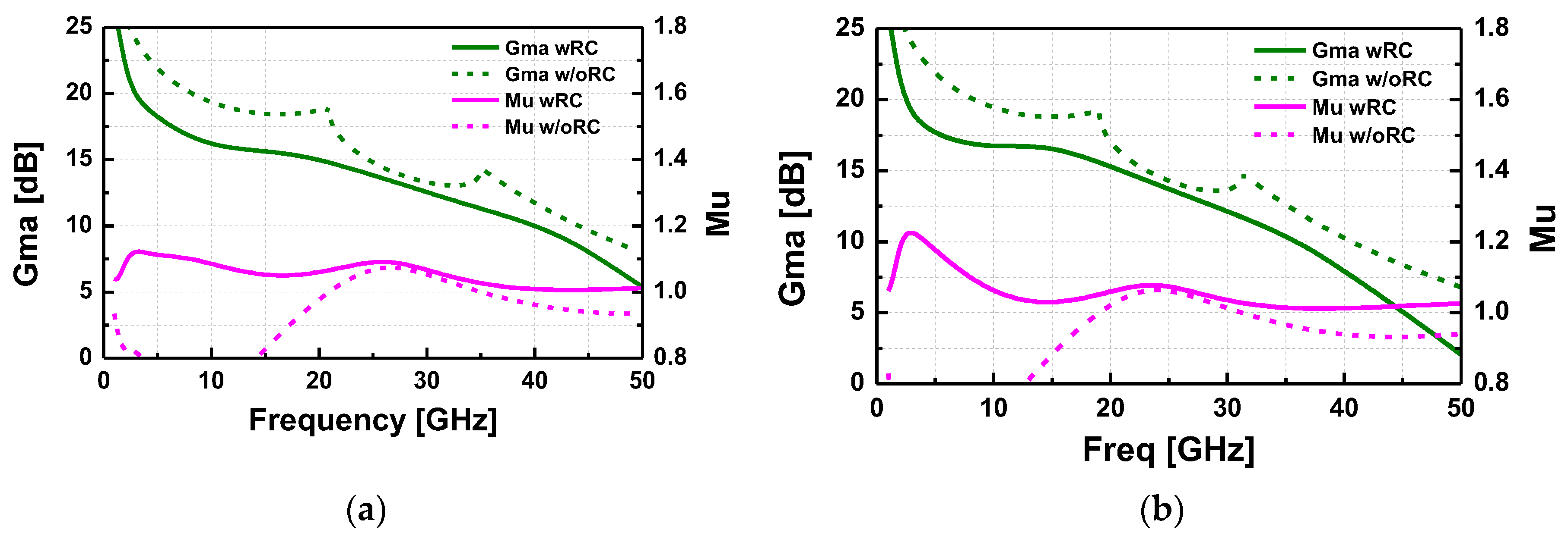
Figure 3.
Series RLC network parameters of the bypass capacitor with de-Qing resistor.
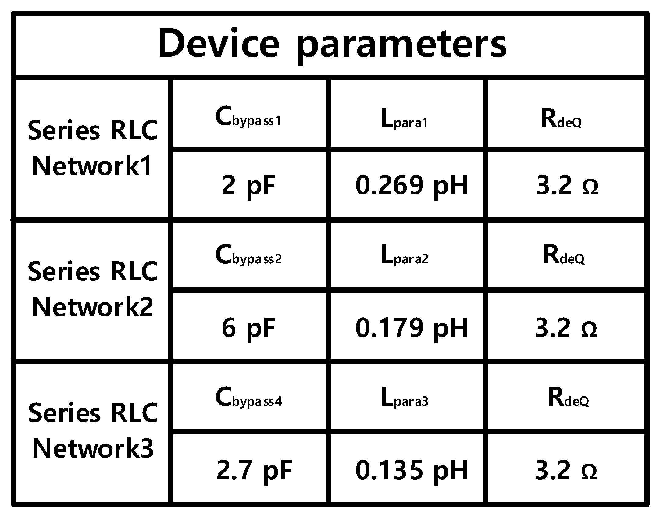
Figure 4.
Implemented stabilization circuits for the parallel HEMT networks.
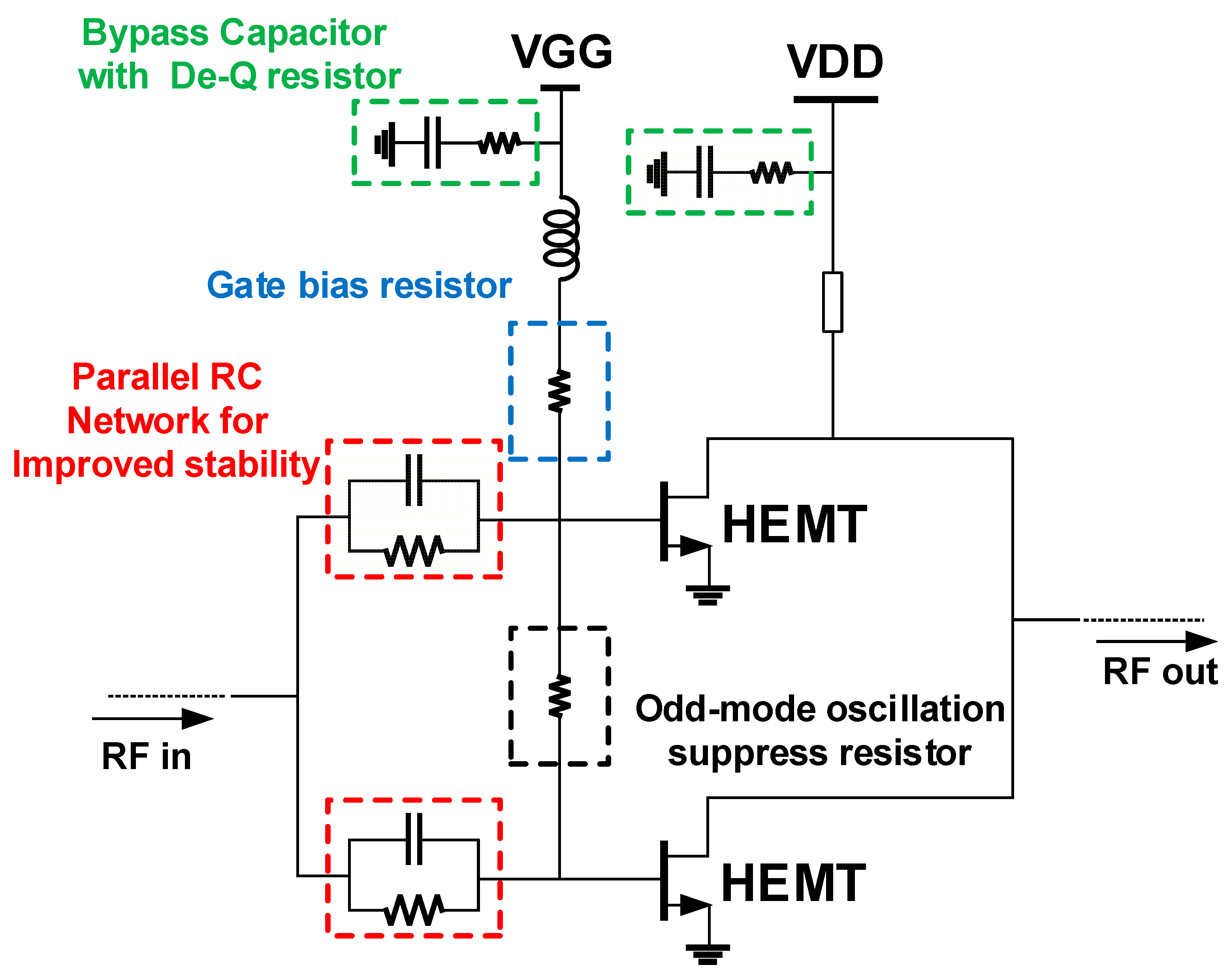
Figure 5.
Load-pull simulation result of 8x50μm OSV HEMT.
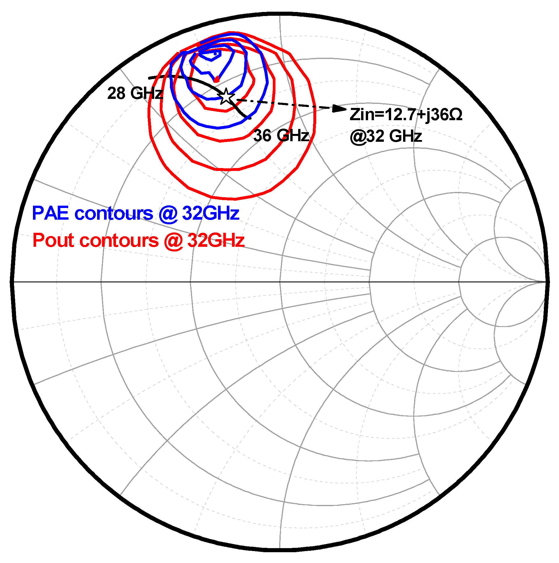
Figure 6.
Photograph of the implemented 32GHz power amplifier.
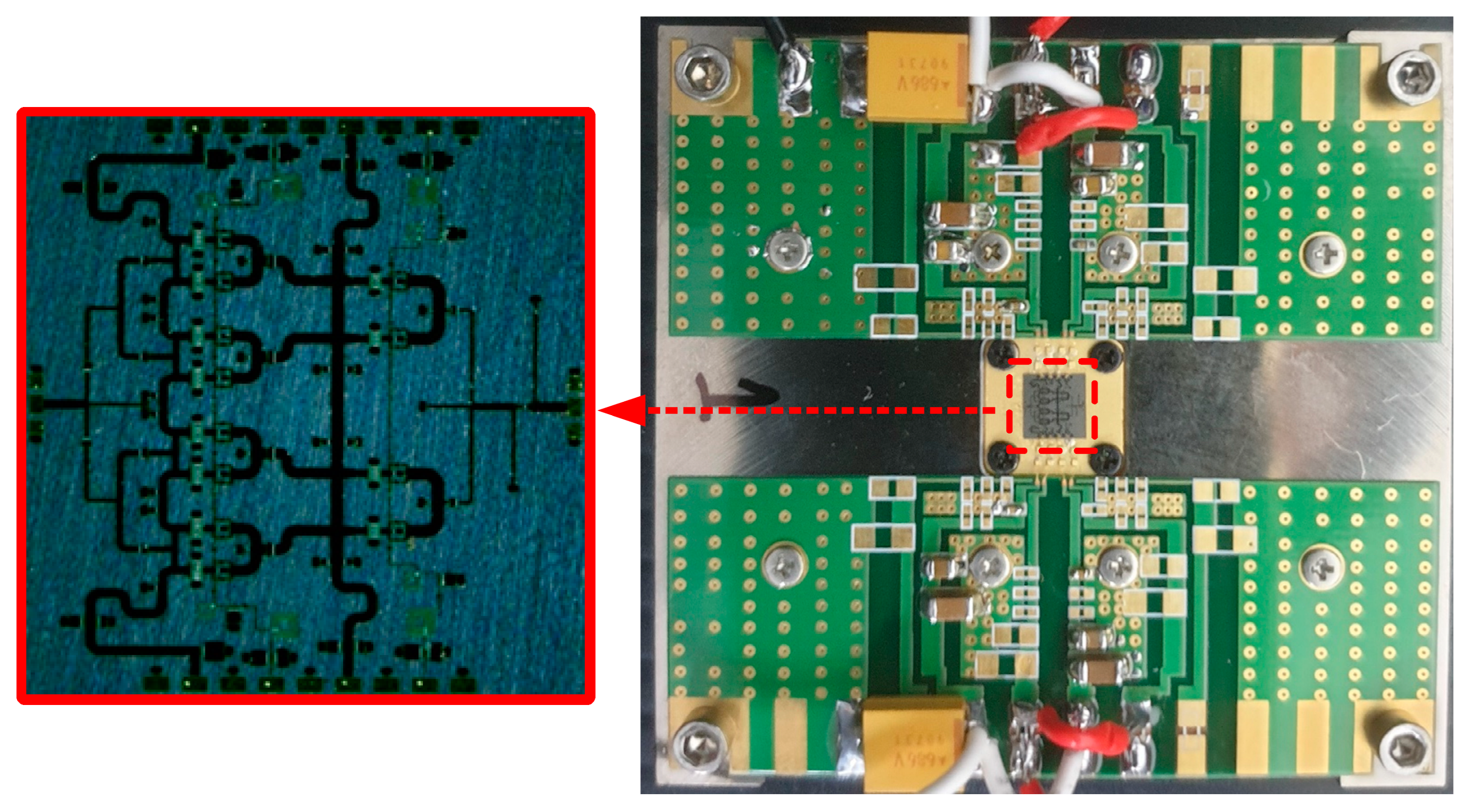
Figure 7.
Small signal measurement setup.
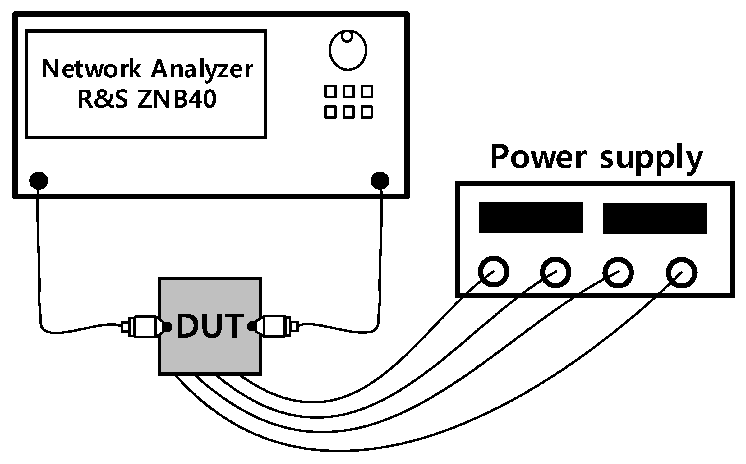
Figure 8.
Large signal measurement setup.
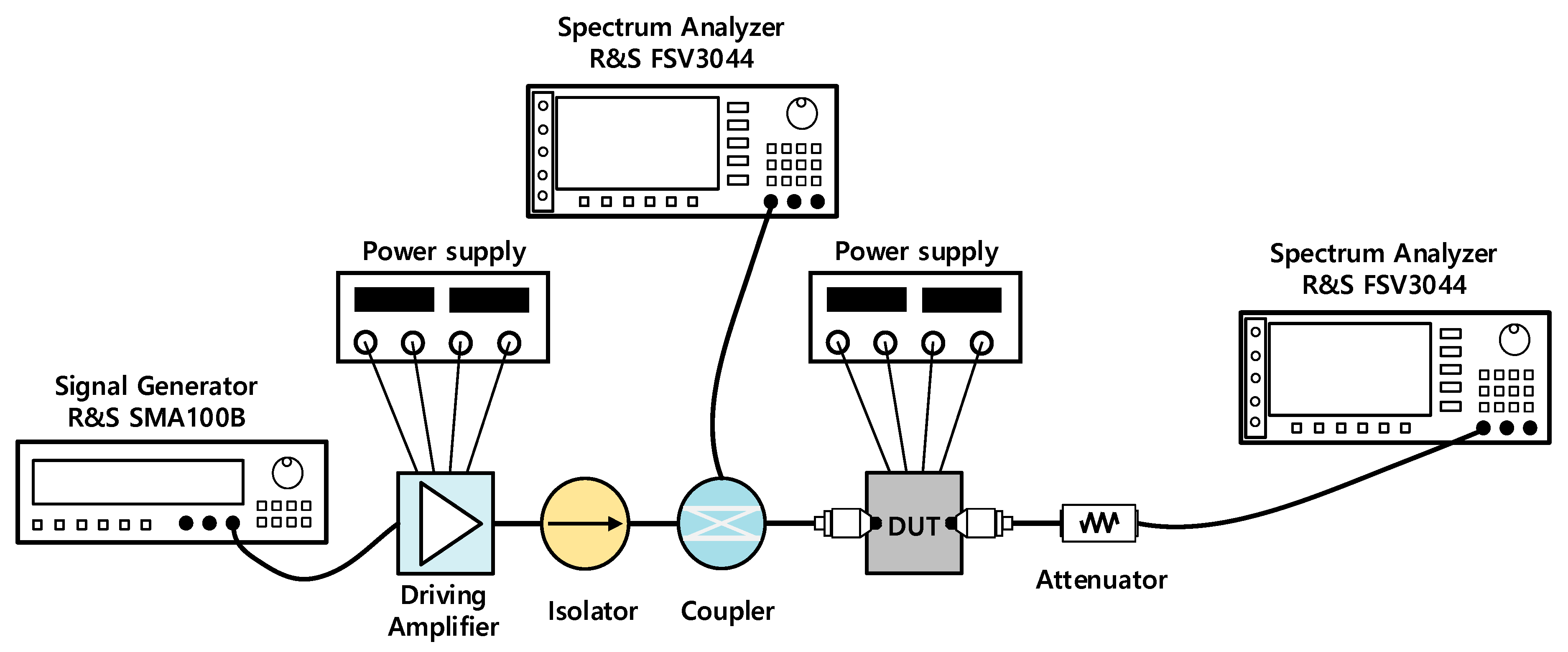
Figure 9.
Small signal performance (a) Large signal performance (b) of simulation and measurement result.
Figure 9.
Small signal performance (a) Large signal performance (b) of simulation and measurement result.
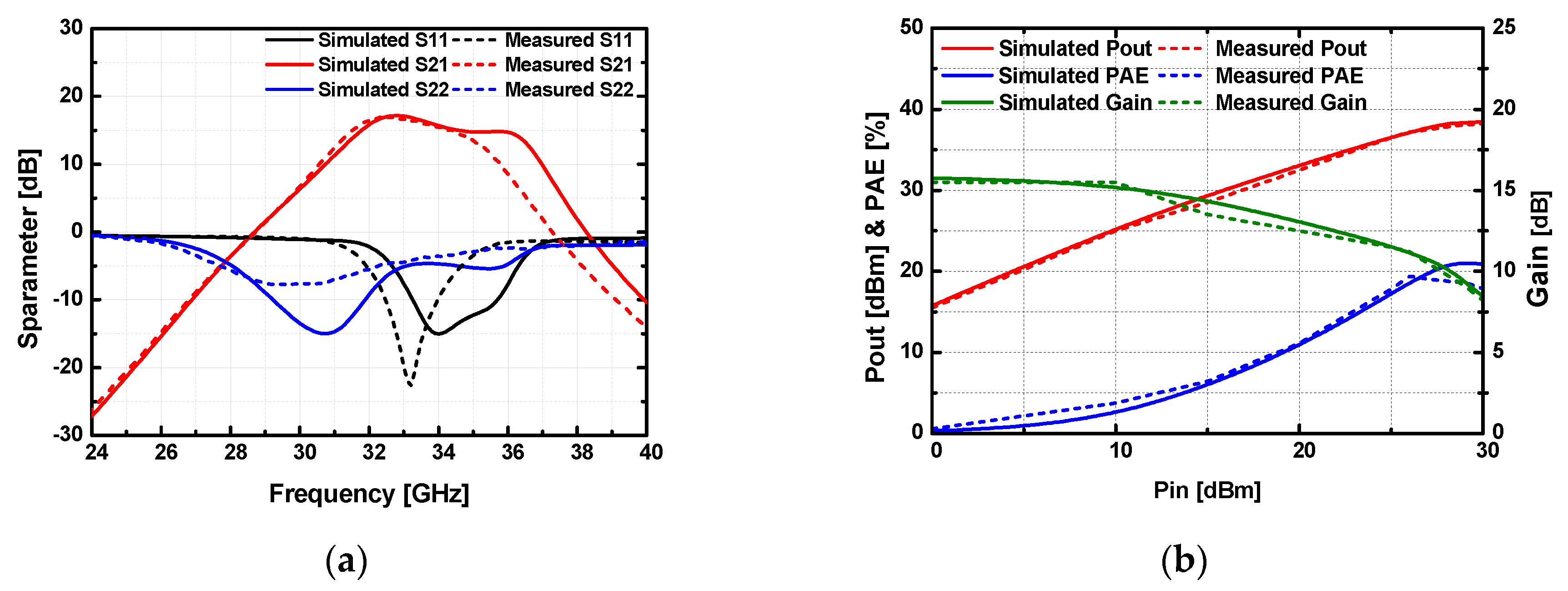

Table 1.
Performance comparison of Ka-band GaN HEMT power amplifiers.
| Ref. | Tech. | Freq. (GHz) | Stages | BW (GHz) |
Small signal Gain (dB) |
Pout (dBm) |
PAE (%) |
Area (mm2) |
| This | 0.15um GaN/SiC | 32 | 2 | 3.5 | 15.9 | 38.3 | 19.3 | 19.35 |
| [8] | 0.15um GaN/SiC | 26.5 | 2 | 2 | 12 | 43.4 | 19.8 | 23.6 |
| [9] | 0.2um GaN/SiC | 31 | 2 | 2 | 10 | 42.6 | 17.4 | 22 |
| [10] | 0.2um GaN/SiC | 30 | 2 | 2 | 10 | 43.3 | 16 | 22 |
| [11] | 0.15um GaN/SiC | 29.5 | 3 | 3 | 28 | 37.8 | 34 | 5.6 |
| [12] | 0.15um GaN/SiC | 29 | 3 | 2.5 | 22 | 39.2 | 29.6 | 11.22 |
| [13] | 0.15um GaN/SiC | 35 | 3 | 6 | 25 | 40.5 | 35 | 9.9 |
Disclaimer/Publisher’s Note: The statements, opinions and data contained in all publications are solely those of the individual author(s) and contributor(s) and not of MDPI and/or the editor(s). MDPI and/or the editor(s) disclaim responsibility for any injury to people or property resulting from any ideas, methods, instructions or products referred to in the content. |
© 2023 by the authors. Licensee MDPI, Basel, Switzerland. This article is an open access article distributed under the terms and conditions of the Creative Commons Attribution (CC BY) license (http://creativecommons.org/licenses/by/4.0/).
Copyright: This open access article is published under a Creative Commons CC BY 4.0 license, which permit the free download, distribution, and reuse, provided that the author and preprint are cited in any reuse.


