
Submitted:
20 June 2023
Posted:
21 June 2023
You are already at the latest version
Abstract
Recently, cobalt iron boron (CoFeB) thin films have been widely investigated to apply to magnetic sensors, due to their high magnetic moment, anisotropy, and stability. However, most of these studies are conducted on rigid silicon substrates. For more diverse applications of magnetic sensors and angle sensors, it is important to explore the properties of ferromagnetic thin films grown on non-rigid deformable substrates. Here, using representative deformable substrates such as polyimide (PI), polyethylene naphthalate (PEN) and polydimethylsiloxane (PDMS) that can be bent or stretched, we report experimental comparison of in-plane magnetic field angle-dependent properties of the amorphous Ta/CoFeB/MgO/Ta thin film which is grown on those deformable substrates. We investigate effects of substrate roughness, tensile stress, characteristics of deformable substrates, and sputtering process on the change of magnetic properties like coercive field (Hc), remanence over saturation magnetization (Mr/Ms), and their biaxial characteristics. This work presents unconventional foundations for exploring deformable magnetic sensors capable of detecting magnetic field angle.
Keywords:
magnetic sensors
; in-plane angle sensors
; CoFeB
; biaxial
; four-fold
; deformable
; flexible
; wearable
; stretchable
1. Introduction
A number of interests in magnetic thin films and magnetic sensors have increased with a variety of effects such as anisotropic magnetoresistance (AMR) [1,2,3,4], giant magnetoresistance (GMR) [5,6,7], tunnel magnetoresistance (TMR) [8,9], Hall effect [10,11], and magneto impedance [12,13]. Especially, studies for improving and analyzing the magnetic properties of magnetic thin films are being actively conducted [14,15]. The magnetic properties of magnetic thin films are affected by spins, orbits, and lattices [16]. These properties are affected by not only the interaction between those three elements inside the thin film, but also the effect of interfaces will be greatly dominant. For this reason, many researchers are studying to understand and applying the changes in the properties of magnetic thin films along with the basic magnetic properties.
There are many applications that uses the magnetic sensors. The magnetic sensors can be utilized in extensive areas like automobile, home appliances, mobile devices, machines, and medical devices. It is particularly useful for sensing changes in motion, such as turning, approaching, or changing speed. In general, the magnetic sensors are usually used with magnets because they detect changes in the magnetic field. For example, when detecting the angle change of a rotating object, the circumference of the rotating object is wrapped with many magnets, and the magnetic sensor detects the change in the magnetic field according to the rotation of the object. There are also magnetic sensors that are used without the magnet, and the application method differs depending on the detectable magnetic field range or sensitivity. Among them, a geomagnetic sensor used as a compass must be manufactured to detect a very weak geomagnetic field. Therefore, the magnetic sensors are required for various devices, and if they can be manufactured in various forms, their utilization will increase.
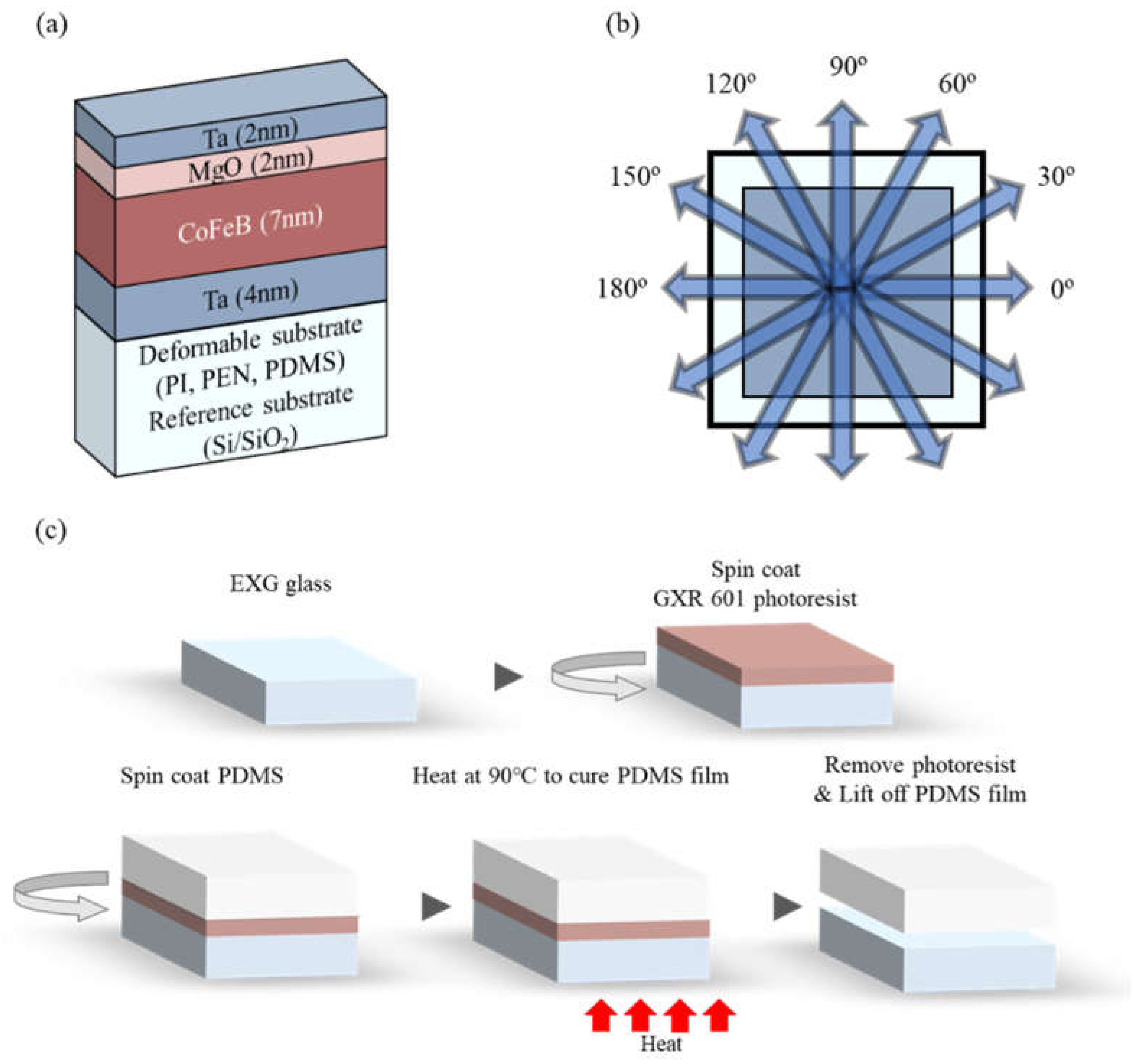
Figure 1.
Schematic images: (a) Sample stack on four different substrates; (b) magnetic field angle on in-plane about the sample (top view); (c) the PDMS substrate fabrication.
Figure 1.
Schematic images: (a) Sample stack on four different substrates; (b) magnetic field angle on in-plane about the sample (top view); (c) the PDMS substrate fabrication.
Bendable and flexible materials have attracted growing interests owing to their potential applications over the last few years in wearable electronics and sensors [17], soft robots [18], light-emitting devices [19], and flexible solar cells [20]. Even, mechanical strain sensing can be added to conventional spintronic devices [6,21,22,23]. The TMR [24,25,26] and AMR [1,3] sensors can be also fabricated on deformable substrates. Stress by deformation of the substrates like bending and stretching can be transferred to the ferromagnetic thin films, inducing compressive or tensile strain to thin films. In several promising studies, it has demonstrated that magnetic anisotropy can be tuned by deriving the strain on the magnetic thin films [27,28,29]. Even recently, it has been studied that the magnetic anisotropy of magnetic thin films can change because they have been grown on the deformable substrate [6,23,30]. However, there are many limitations when annealing or patterning the magnetic thin films on the deformable substrate, due to the need for caution in high temperatures and chemical processes. In addition, in order to manufacture a flexible device, a deformable material is used as a substrate, and the flexibility of the substrate is important, but it is an essential part to select materials and process methods to be formed on the flexible substrate. This is because, even if a deformable substrate having good flexibility is used, the thin film is peeled off if the material to be grown on has poor deformability or poor adhesion to the substrate. Also, how to form a magnetic thin film on such a deformable substrate is an important factor, but a method of analyzing changes in properties when bending or stretching is applied to the device is also important.
As a basis study of a deformable magnetic sensor (or deformable in-plane angle sensor in which the rotation axis is in the normal direction of the sample plane), the magnetic properties of the magnetic thin film on the deformable substrate are analyzed in various ways. The amorphous Ta/CoFeB/MgO/Ta thin film, widely used as the ferromagnetic thin film [11,26,31], was sputtered with other thin layers like tantalum (Ta) and magnesium oxide (MgO) thin films on various flexible and stretchable substrates which are polyethylene naphthalate (PEN), polyimide (PI), and polydimethylsiloxane (PDMS). We use the amorphous Ta/CoFeB/MgO/Ta thin films grown on the deformable as blanket films without annealing and patterning processes. And, the Ta was used as a seed layer to improve the adhesion between the substrate and the Ta/CoFeB/MgO/Ta thin film, and a sputtering process capable of physically strongly forming a thin film was applied. Also, we investigate magnetic properties like the biaxial Hc and Mr/Ms by each characteristic of the substrates, and phase difference when the PDMS sample is stretched. At the same time, we show foundational analysis of the amorphous Ta/CoFeB/MgO/Ta thin films to propose methods to apply them to the various magnetic sensors or the in-plane magnetic field angle sensor which are flexible or stretchable.
2. Materials and Methods
2.1. Sample Fabrication
For comparison of deformable substrates, we have used three deformable substrates (PI, PEN, and PDMS) and one rigid Si/SiO2 substrate. The substrate size is 4 mm × 4 mm, and its thickness is about 0.6 mm. To investigate the magnetic properties of amorphous CoFeB thin films sputtered onto a variety of deformable substrates, we grew the magnetic thin films, Ta(4)/CoFeB(7)/MgO(2)/Ta(2) (thickness, nm), on the substrates. The 4 nm thick Ta is a seed layer. The MgO(2)/Ta(2) is cap layers. Composition ratio of the CoFeB is 40:40:20 in order. And we used three sputter guns tilted at 45 degrees (θ = 45°, Figure 2). The three sputter guns were mounted 120 degrees (φ = 120°) apart from each other. An edge of all substrates was placed parallel to the tangent of the circular sample holder so that the outer direction of the sample holder was 0 degrees (φ = 0°) and the inner direction was 180 degrees (φ = 180°) to the normal direction of the tangent. The sample holder diameter is 6 inches.
After pre-sputtering process, the Ta/CoFeB/MgO/Ta thin films were grown at a base pressure of 3×10⁶ Torr via DC-RF magnetron sputtering onto substrates placed on a sample holder rotating at 10 rpm (Figure 1a and Figure 2). During main sputtering, the working pressure, power, and gas flow rate are different depending on the materials. In order of Ta, CoFeB, and MgO, respectively, the working pressure was 10 mTorr, 4 mTorr, and 0.8 mTorr, and the power was 20 W, 50 W, and 150 W, and the gas flow rate was 10 sccm, 10 sccm, and 4 sccm.
Among the substrates, only a PDMS substrate, which could be torn, was directly manufactured. So, the fabrication methods of the PDMS substrate was exhibited in 2.2 below.
2.2. PDMS Substrate Fabrication
The PDMS (Dow Corning) materials were prepared at a base-to-curing agent volume ratio of 10:1, and the mixture was degassed for 1 hour. A 2 cm × 2 cm glass substrate was cleaned with acetone, methanol, and deionized water for 15 min under ultrasonication. After cleaning, positive photoresist (PR) AZ GXR-601 (Merk) was spin-coated at a speed of 1500 rpm for 30 sec and baked on a hotplate at 95 °C for 1 min. The degassed PDMS mixture was then spun at 500 rpm for 20 sec on PR-coated glass and cured on a hotplate at 90 °C for 1 hour. To cure the PDMS film completely, it was held undisturbed for 24 hours. Finally, acetone was used to remove PR and detach the completely cured PDMS film from the glass. The overall fabrication process is illustrated in Figure 1c.
2.3. Measurement
To identify the crystal structure of the Ta/CoFeB/MgO/Ta thin films sputtered on various substrates, the substrates with and without the Ta/CoFeB/MgO/Ta thin film were analyzed via X-ray diffractometry (XRD; SmartLab, Rigaku). The power of the X-ray was 9 kW (45 kV, 200 mA), and a Cu target source with a wavelength of 0.15412 nm was used. The surface profiles and roughness of the substrates were measured by using atomic force microscopy (AFM; XE100, PSIA). The magnetic properties, including the saturation magnetization (Ms) and coercive field (Hc), were measured by using superconducting quantum interference vibrating sample magnetometry (SQUID-VSM; MPMS3 system provided by KBSI; Quantum Design). Using the SQUID-VSM equipment, a magnetic hysteresis loop (M-H loop) according to the angle was derived, while applying a magnetic field from 0 degrees (φ = 0°) to 360 degrees (φ = 360°) in the in-plane direction of the sample (Figure 1b). Magnetic force microscopy (MFM; XE100, PSIA) was used to investigate microscopic magnetic properties like magnetic phase of magnetic domains in the magnetic thin films on the stretchable PDMS substrates with tensile strain. The tip of the MFM probe was coated with cobalt magnetized in perpendicular direction.
3. Results and Discussion
3.1. Optical analysis via XRD
The amorphous properties of the Ta/CoFeB/MgO/Ta thin films sputtered on various deformable substrates were characterized using the XRD. As all the Ta/CoFeB/MgO/Ta thin films were sputtered at room temperature without annealing, the CoFeB thin film was expected to have an amorphous structure. The Figure 3a,b shows the XRD peaks of bare substrates and the Ta/CoFeB/MgO/Ta thin films grown on various substrates, respectively. Figure 3c shows detailed XRD data for the bare PDMS substrate and the Ta/CoFeB/MgO/Ta thin film sputtered on the PDMS substrate. Likewise, Figure 3d shows detailed XRD data for the bare PI substrate and the Ta/CoFeB/MgO/Ta thin film sputtered on the PI substrate. The XRD data for the Ta/CoFeB/MgO/Ta thin film sputtered on all the investigated substrates were similar and showed the same peaks as those of bare substrates. In case of the PEN substrate, the peaks appeared around 27° and 56° [32]. The peaks of the PDMS and PI substrate were observed at 11° [33] and 21° [34], respectively. Other peaks such as Ta, CoFeB, and MgO were never seen except for only the substrates. The amorphous thin films show broad and low peaks in XRD graphs [35]. So, they were buried in peaks of the substrates of higher intensity. This exhibits that all the peaks in Figure 3 originate from the bare substrates. Therefore, it was proved that the Ta/CoFeB/MgO/Ta thin film has an amorphous structure, regardless of the substrate.
3.2. Magnetic Properties with Deformable Substrates
The effects of various deformable substrates were investigated by comparing the magnetic properties of the Ta/CoFeB/MgO/Ta thin films sputtered onto the substrates. The magnetic properties were extracted from the M-H loop measured when an in-plane magnetic field was applied using the SQUID-VSM. As shown in Figure 4, it was confirmed that all Ta/CoFeB/MgO/Ta thin films on various substrates exhibited in-plane magnetic anisotropy through having rectangular M-H loops in the case of in-plane, unlike the case of out-of-plane [16].
We can derive various magnetic properties such as saturation magnetization, remanence, coercive field, magnetic anisotropy field (Hk), and magnetic anisotropy constant (K) from the M-H loop [36]. In the case of the magnetic anisotropy constant, K, it is one of the important elements in a sensor which detects the magnetic field angle, and indicator for evaluating the magnetic anisotropy. To know the value of K, however, we must not only know the exact hard axis, Ms, and Hk, but also other various analysis [37]. In magnetic anisotropy energy (Ea) (see Equation (1)), K0 is an isotropic term that is not affected by angle, Ku is a uniaxial anisotropy constant, and Kc is a magneto-crystalline anisotropy constant that contributes to four-fold symmetry (or biaxial characteristics) [16,37,38]:
In magnetic thin films with in-plane magnetic anisotropy, hard axis is formed in the normal direction of most planes by shape anisotropy due to thin thickness and wide area [16,36]. So, analyzing the magnetic anisotropy of the plane’s normal direction is not appropriate for assessing sensors that sense the in-plane magnetic field angle. Instead, we obtained the magnetic anisotropy field between the in-plane magnetic anisotropy and the out-of-plane magnetic anisotropy for each sample, and did not calculate the magnetic anisotropy energy separately. The magnetic anisotropy fields are about 8.2 kOe (Si/SiO2), 6.3 kOe (PDMS), 3.5 kOe (PI), and 13 kOe (PEN), respectively.
Even, we did not proceed with crystallization of the Ta/CoFeB/MgO/Ta thin films through annealing process. And, here, we focus on base studies for magnetic sensors and especially in-plane magnetic field angle sensors. Therefore, we only analyzed the angle dependence of Hc and Mr/Ms which can be quickly identified according to the substrates. In general, in the magnetic thin film research, the Hc change indicates the presence or absence of pinning effects of the magnetic domain movements due to substrate roughness or impurities [36], and Mr/Ms change implies that multi-grains or magnetic domains are composed of magnetic anisotropies of various orientation [39,40]. These two values (Hc and Mr/Ms) are one of the practical elements for qualitatively evaluating the magnetic anisotropy of a sample [38,41,42].
As depicted in Figure 4 and Figure 5a,c, all magnetizations (M) were normalized into saturation magnetization (Ms ~ 1100 emu/cc) of each sample with the substrate to compare the variation with magnetic field angle in each sample. So, we used M/Ms as y-axis of M-H loop. In this article, we represented M/Ms-H loop as M-H loop for readability. Figure 5a,c shows the case where the magnetic field is applied at 0° and 90°, respectively. When the magnetic field is applied at 0° (Figure 5a), there is no significant difference in the shape of the M-H loop depending on the substrate, except for the sample in which the Ta/CoFeB/MgO/Ta thin film is grown on the Si/SiO2 substrate. For the Si/SiO2 sample, the rectangular shape of the loop was the most prominent among the four samples (Si/SiO2, PDMS, PI, and PEN). The rectangular shape of the M-H loop means that the sample has good magnetic anisotropy and quick magnetic switching property. Whereas, in the case of 90° (Figure 5b), the shapes of the M-H loops were clearly different depending on each substrate, and it can be seen that a large difference occurs in the value of the Hc and Mr/Ms (see Table 1). The Hc increased when the angle of the magnetic field changed from 0° to 90°. In the PEN sample with the largest change, the Hc increased by about 4 times from Hc,0° = 20.96 Oe to Hc,90° = 84.35 Oe. This value (Hc,90° = 84.35 Oe) is about 6.6 times larger than the 90° value of Si/SiO2 sample (Hc,90° = 12.65 Oe) (Table 1). This result is related to the roughness of the substrate surface. As the roughness increases, the pinning effect intensifies, and eventually the Hc increases in proportion to the roughness. As shown in Figure 5c,d, Si/SiO2 and PDMS samples with alike roughness have similar Hc values, and PI and PEN samples with large roughness also tend to have large Hc values. Looking at the y-axis scales in Figure 5b,d, it can be seen that range of y-axis scale is much smaller when the angle of the magnetic field is 0° than 90°. Through curve fit, we can know that both angles show similar tendencies.
However, it is hard to explain that the Hc change with magnetic field angle only by the pinning effect. Mostly, the Mr/Ms changes by variation of magnetic anisotropy orientations of multi-grains, and the Hc are affected by grain size of them [43]. So, the effect is noticeable in case of deformable substrates which have rough and bumpy surfaces, because it is easy for rough and bumpy surfaces to make multi-grains of magnetic thin films by physically dividing areas. So, unlike the Si/SiO2 and PDMS samples having smooth surfaces, the rough PI and PEN samples had a substantial variation in Hc between the magnetic field angles 0° and 90°, which does not exist only between the two angles. Similarly, the Mr/Ms became smaller at 90° than at 0° since the magnetic anisotropy of each grain is formed in many directions. The Mr/Ms and Hc continuously change from 0° to 360° of the magnetic field angles. We guessed that this influence of multi-grains is one of the causes of biaxial characteristics. Detailed its analysis is conducted in 3.3 with Figure 7 and Table 2.
3.3. Angular Dependence of Hc and Mr/Ms
Since we focus on research that will be based on the magnetic sensors to be used as the in-plane angle sensors, the M-H loops of all samples were measured in the in-plane directions at 30° intervals from 0° to 360° (see Figure 6).
Figure 6.
Angle dependence of Hc and Mr/Ms of (a) Si/SiO2; (b) PDMS; (c) PI; and (d) PEN from 0° to 360° in polar coordinate system.
Figure 6.
Angle dependence of Hc and Mr/Ms of (a) Si/SiO2; (b) PDMS; (c) PI; and (d) PEN from 0° to 360° in polar coordinate system.
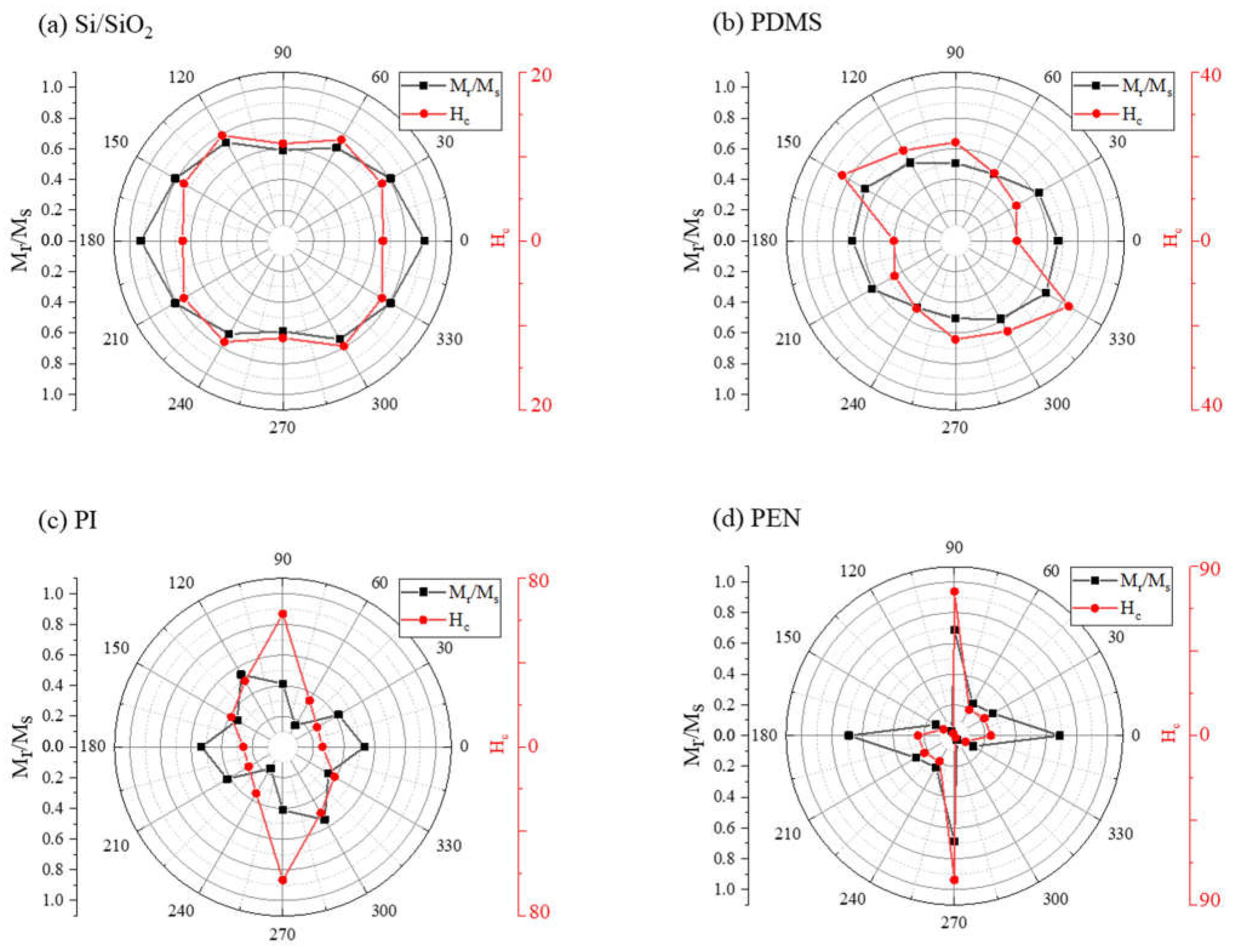
The in-plane easy axis of all the samples was formed by shape anisotropy, because the amorphous CoFeB thin film is very thin of 7 nm. For the same reason, the hard axis was formed in the direction perpendicular to the plane. So, the Si/SiO2 sample showed isotropic properties for both Hc and Mr/Ms. However, it had not a perfect isotropic shape in a polar coordinate system. This impact is due to our sputtering system. Our sputter was equipped with the 45° (φ = 45°, Figure 2) tilted sputter gun, and the sample holder rotates at 10 rpm. So, when sputtering is progressing while the sample holder rotates, the energy applied to the substrate is different according to the direction of the sample, and consequently, the stress transferred to the thin film is different depending on the direction of the sample [44].
Figure 7.
M-H loops with magnetic field angle from 0° to 150° of (a) PI sample; and (b) PEN sample.
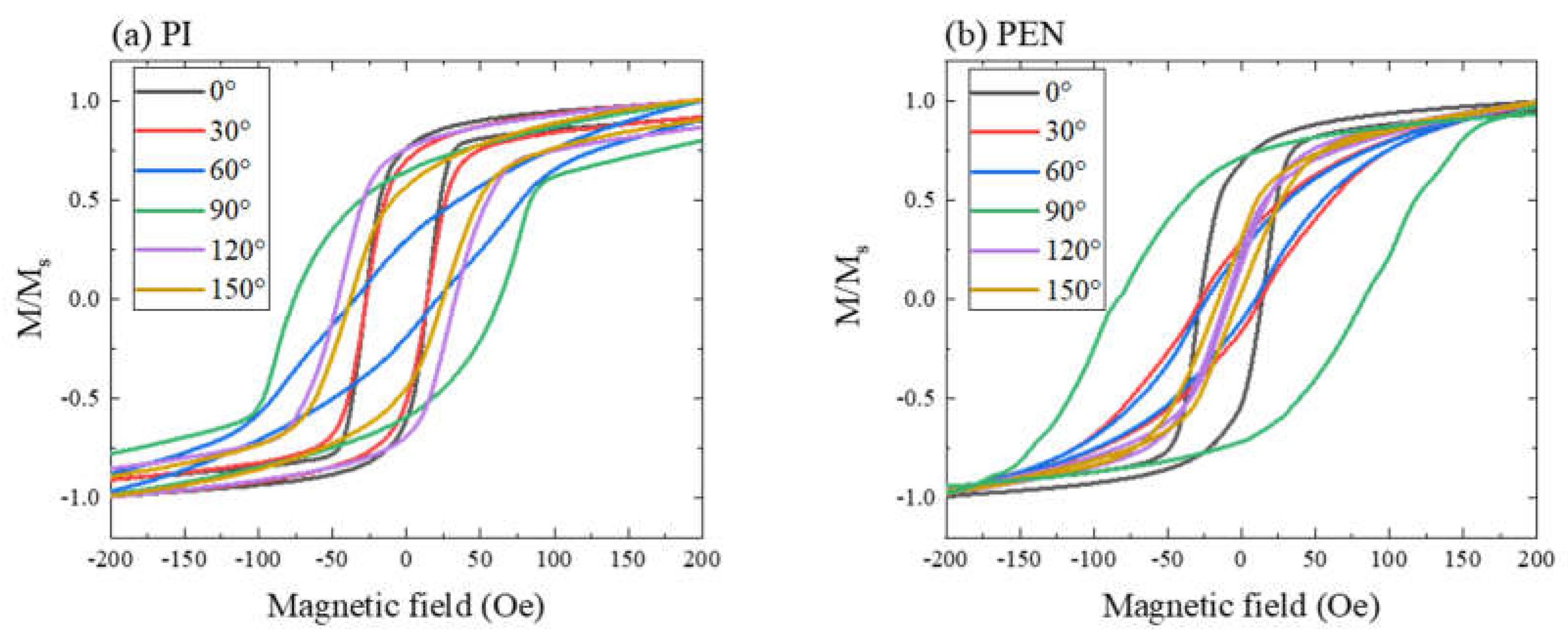

Table 2.
Rq, Hc, and Mr/Ms with substrates at 0° and 90°.
| Angle | Hc, Oe | Mr/Ms | ||
|---|---|---|---|---|
| PI | PEN | PI | PEN | |
| 0° | 0.259 | 0.239 | 0.533 | 0.691 |
| 30° | 0.258 | 0.227 | 0.420 | 0.290 |
| 60° | 0.349 | 0.194 | 0.162 | 0.243 |
| 90° | 0.866 | 0.937 | 0.413 | 0.690 |
| 120° | 0.496 | 0.016 | 0.546 | 0.034 |
| 150° | 0.389 | 0.083 | 0.345 | 0.141 |
This stress or strain is related to the magnetostriction effect. In particular, the CoFeB is one of the materials with a large magnetostriction constant (λs = 31×10-6) [36,45]. For this reason, the sample sputtered onto the Si/SiO2 substrate did not have fully isotropic properties. In the sample of the PDMS substrate, which has a slightly rougher surface than the Si/SiO2 sample, the Mr/Ms was somewhat isotropic, but the Hc wasn’t isotropic. In contrast, the PI and PEN samples exhibited either uniaxial or biaxial characteristics. As depicted in Figure 6c, the Hc of the PI sample had maximum values at 90° and 270°. It showed minimum values at 0° and 180° with the uniaxial property. The Mr/Ms of PI sample had high values at 0°, 120°, 180°, and 300°. Its low values appeared at 60°, 150°, 240°, and 330°, so, it had four-fold symmetry (or biaxial characteristic). In Figure 6d, the PEN sample also revealed biaxial characteristics for both Hc and Mr/Ms. The Hc of the PEN sample has seemed almost uniaxial due to the large difference between the values of 90° (or 270°) and 0° (or 180°), whereas the Mr/Ms had almost the same high values at 0°, 90°, 180°, and 270°. It had also the same low values at 60°, 120°, 240°, and 300°. The PEN sample had a complete biaxial characteristic in both Hc and Mr/Ms. The detailed M-H loops of the PI and PEN samples according to the angle of applied magnetic field were exhibited in Figure 7a,b, respectively. For visibility, only the angles from 0° to 150° were inserted.
The biaxial characteristics of the PI and PEN samples were also analyzed due to the influence of our sputtering method. Because our samples were not annealed, it is difficult to see the effect of magneto-crystalline anisotropy. Even, they were not patterned to have shape anisotropy characteristics. The same large Hc and Mr/Ms at 90° and 270° in the PEN sample can’t be explained simply by the effect of the large roughness of the substrate. Unlike rigid Si/SiO2 substrates, the PDMS, PI, and PEN substrates are deformable substrates which have soft and bumpy surface and have a large interaction with thin films on its when it is being strained. So, the influence due to the stress between the substrate and the thin film acts more strongly than the case of the Si/SiO2 sample, and each substrate has different characteristics. However, the Ta/CoFeB/MgO/Ta thin film may have been formed in a directional shape to be able to have shape anisotropy on the deformable substrate because of the stress as well as the non-rigid surface of the deformable substrates. Therefore, we analyzed that the Ta/CoFeB/MgO/Ta thin film may have the biaxial anisotropy by shape anisotropy owing to the directional shape. It’s just that the size of the shape might have been formed with a micrometer scale or much smaller than that.
If the cause of all these phenomena is more clearly identified and applied, it is expected that various applications will be possible as deformable magnetic sensors. The magnetoresistance depends on the magnetic anisotropy, and it is related to Hc and Mr/Ms [29,46,47,48]. So, for example, controlling magneto-crystalline anisotropy through annealing or forming shape anisotropy by patterning a magnetic thin film will enable effective magnetic sensors or in-plane angle sensors to be fabricated.
3.4. Strain Effects in the CoFeB Thin Film Sputtered on the PDMS Substrate
The effects of physical deformation (tensile strain in one direction) of the Ta/CoFeB/MgO/Ta thin film sputtered on the PDMS substrate was investigated at the macroscopic and microscopic scales using the SQUID-VSM and MFM, respectively. For each measurement, all stretched samples were placed on 4 mm × 4 mm glass substrates with 5% strain. This method is necessary for accurate measurement of stretchable samples. However, in the case of SQUID-VSM measurement, the magnitude of the detected magnetic moment may vary due to the change in the position of the Ta/CoFeB/MgO/Ta thin film on the sample holder, so it is recommended to apply a normalization operation. In addition, due to the characteristics of SQUID-VSM measurement in which the sample is shaken with rapid vibration of about 80 Hz, the sample must be firmly attached to the glass substrate to prevent separation due to rapid vibration transmitted to the sample. Hence, measuring the change in the properties by bending of the sample was difficult to implement, so it was not carried out. Moreover, even in MFM measurement, the distance between the sample and the tip of the MFM probe must be constant, but it is very difficult to maintain the bent sample at a constant distance.
The overall M–H loops are shown in Figure 8a with before, with, and after 5% strain. The Hc of the PDMS sample before and after strain were not significantly different. However, with tensile strain, the Hc of the sample slightly increased, suggesting that a few grains formed anisotropy in a direction away from the applied direction of the magnetic field. Also, for the same reason, we ensured that strain tends to stabilize in-plane magnetization owing to the induced tensile stress [49] by confirming that histogram of with strain was firmed high and narrow around 0° phase (Figure 8b). Only with strain did the magnetic phase deviate from 0 degrees and shifted by 0.04°. It explains that the orientation of magnetic anisotropy has changed.
Table 3.
The Hc and Mr/Ms values with before, with, and after strain of the PDMS sample.
| Condition | Hc | Mr/Ms |
|---|---|---|
| Before strain | 16.12 | 0.645 |
| With strain | 29.07 | 0.625 |
| After strain | 12.41 | 0.485 |
The histogram of the after strain sample was wide. It was interpreted that the orientation of magnetic anisotropy was affected as the surface of the magnetic thin film became more uneven due to the fine scratches that occurred after stretching the sample. Thus, in order to use this sample as a mechanical strain sensor, it is recommended to artificially damage the sample by repeating the tensile operation several times and use it after the magnetic anisotropy orientation is stabilized. We anticipate that more precise measurement will be possible if a mechanical strain sensor based on spintronic devices is used together with the existing mechanical strain sensor.
The Hc, Mr/Ms, and magnetic phase were tuned by the tensile stress applied to the magnetic thin film, indicating that magnetic anisotropy orientation can be tuned by strain. Controlling the magnetic anisotropy is essential for adjusting the performance of the magnetic sensors or mechanical strain sensors [1,3].
4. Conclusions
The magnetic properties of ferromagnetic materials sputtered on various deformable substrates should be studied for application in the deformable or wearable magnetic sensors. The CoFeB is a suitable material in the magnetic sensor as the ferromagnetic layer because it has a large magnetic moment and tunable magnetic anisotropy. The magnetic properties of the amorphous CoFeB thin film sputtered on various substrates varied even for the same the amorphous CoFeB thin film with the same thickness. This properties can be used to be variously applied in the magnetic sensors.
The roughness of the substrate has a significant impact on Hc because of the pinning effect of the magnetic domains. The Hc and Mr/Ms of our samples depends on magnetic field angle. Comparing the Hc of the PEN sample when the magnetic field angle is 90° and the Hc of the Si/SiO2 sample when the magnetic field angle is 0°, the case of the PEN sample was 6.6 times larger. Even though the CoFeB thin film was not annealed and not patterned to have magnetic anisotropy, the biaxial properties of the Hc and Mr/Ms were affected by the stress between deformable substrates and the Ta/CoFeB/MgO/Ta thin films, which the sputtering has an effect on. The biaxial properties of Hc and Mr/Ms are important because they can qualitatively explain that magnetic anisotropy energy is able to have the biaxial properties. Especially, the Mr/Ms of PI and PEN sample clearly exhibited the biaxial characteristics. Additionally, with a tensile strain of 5%, the magnetic phase was shifted by 0.04°. After the strain release, the magnetic anisotropy of the grains did not return to its original state, but the average magnetic phase did not change.
We believe that all these effects will be appropriately used in magnetic sensors or deformable angle sensors.
Author Contributions
Conceptualization, A.H.J., and Y.H.H.; methodology, A.H.J., J.S., and B.K.; formal analysis, A.H.J. and Y.H.H.; investigation, A.H.J., J.S.L., and Y.H.H.; resources, B.-K.J.; data curation, A.H.J.; writing—original draft preparation, A.H.J. and Y.H.H.; writing—review and editing, A.H.J., Y.H.H., S.L., S.H.S., and B.K.; supervision, B.-K.J.; funding acquisition, B.-K.J. All authors have read and agreed to the published version of the manuscript.
Funding
Not applicable.
Institutional Review Board Statement
Not applicable.
Informed Consent Statement
Not applicable.
Data Availability Statement
Not applicable.
Acknowledgments
This work was supported by the Brain Korea 21 Plus Project in 2023, Samsung Electronics Co., Ltd. (No. IO201214-08159-01), and Korea Institute for Advancement of Technology (KIAT) grant funded by the Korea Government (MOTIE) (P0020967, Advanced Training Program for Smart Sensor Engineers).
Conflicts of Interest
The authors declare no conflict of interest.
References
- Chen, J. and Zhang, Z. A flexible anisotropic magnetoresistance sensor for magnetic field detection. Journal of Materials Science: Materials in Electronics 2023, 34, 73. [Google Scholar] [CrossRef]
- Dai, Y. , Zhao, Y., et al. Fourfold Anisotropic Magnetoresistance of L 1 0 FePt Due to Relaxation Time Anisotropy. Physical Review Letters 2022, 128, 247202. [Google Scholar] [CrossRef]
- Wang, Z. , Wang, X., et al. Highly sensitive flexible magnetic sensor based on anisotropic magnetoresistance effect. Advanced Materials 2016, 28, 9370–9377. [Google Scholar] [CrossRef] [PubMed]
- Fina, I. , Marti, X., et al. Anisotropic magnetoresistance in an antiferromagnetic semiconductor. Nature communications 2014, 5, 4671. [Google Scholar] [CrossRef] [PubMed]
- Fert, A. and Van Dau, F.N. Spintronics, from giant magnetoresistance to magnetic skyrmions and topological insulators. Comptes Rendus Physique 2019, 20, 817–831. [Google Scholar] [CrossRef]
- Ota, S. , Ando, A., and Chiba, D. A flexible giant magnetoresistive device for sensing strain direction. Nature Electronics 2018, 1, 124–129. [Google Scholar] [CrossRef]
- Kubota, T. , Wen, Z., and Takanashi, K. Current-perpendicular-to-plane giant magnetoresistance effects using Heusler alloys. Journal of Magnetism and Magnetic Materials 2019, 492, 165667. [Google Scholar] [CrossRef]
- Fujiwara, K. , Oogane, M., et al. Magnetocardiography and magnetoencephalography measurements at room temperature using tunnel magneto-resistance sensors. Applied Physics Express 2018, 11, 023001. [Google Scholar] [CrossRef]
- Liu, X. , Liu, C., et al. Design and implementation of a multi-purpose TMR sensor matrix for wireless electric vehicle charging. IEEE Sensors Journal 2018, 19, 1683–1692. [Google Scholar] [CrossRef]
- Paun, M.-A. , Sallese, J.-M., and Kayal, M. Hall effect sensors design, integration and behavior analysis. Journal of Sensor and Actuator Networks 2013, 2, 85–97. [Google Scholar] [CrossRef]
- Zhu, T. , Chen, P., et al. Giant linear anomalous Hall effect in the perpendicular CoFeB thin films. Applied Physics Letters 2014, 104, 202404. [Google Scholar] [CrossRef]
- Melnikov, G.Y. , Lepalovskij, V.N., et al. Magnetoimpedance thin film sensor for detecting of stray fields of magnetic particles in blood vessel. Sensors 2021, 21, 3621. [Google Scholar] [CrossRef] [PubMed]
- Chen, Y. , Zou, J., et al. Enhanced giant magneto-impedance effects in sandwich FINEMET/rGO/FeCo composite ribbons. Applied Surface Science 2021, 545, 149021. [Google Scholar] [CrossRef]
- Dc, M. , Shao, D.-F., et al. Observation of anti-damping spin–orbit torques generated by in-plane and out-of-plane spin polarizations in MnPd3. Nature Materials 2023, 1–8. [Google Scholar] [CrossRef]
- Peng, S. , Wang, M., et al. Origin of interfacial perpendicular magnetic anisotropy in MgO/CoFe/metallic capping layer structures. Scientific reports 2015, 5, 18173. [Google Scholar] [CrossRef]
- Cullity, B.D. and Graham, C.D., Introduction to magnetic materials. John Wiley & Sons, 2011.
- Zhu, C. , Wu, J., et al. Advanced fiber materials for wearable electronics. Advanced Fiber Materials 2023, 5, 12–35. [Google Scholar] [CrossRef]
- Chi, Y. , Li, Y., et al. Bistable and multistable actuators for soft robots: Structures, materials, and functionalities. Advanced Materials 2022, 34, 2110384. [Google Scholar] [CrossRef]
- Yao, Y. , Chen, Y., et al. A robust vertical nanoscaffold for recyclable, paintable, and flexible light-emitting devices. Science Advances 2022, 8, eabn2225. [Google Scholar] [CrossRef]
- Zhao, Q. , Shen, H., et al. Effect of CZTS/CCZTS Stacked Structures Prepared through Split-Cycle on the Performance of Flexible Solar Cells. ACS Applied Energy Materials 2022, 5, 3668–3676. [Google Scholar] [CrossRef]
- Anwarzai, B. , Ac, V., et al. Pseudo spin-valve on plastic substrate as sensing elements of mechanical strain. Vacuum 2009, 84, 108–110. [Google Scholar] [CrossRef]
- Áč, V. , Anwarzai, B., et al. Influence of mechanical strain on magnetic characteristics of spin valves. in Journal of Physics: Conference Series, 2008; IOP Publishing. [Google Scholar] [CrossRef]
- Matsumoto, H. , Ota, S., et al. A flexible exchange-biased spin valve for sensing strain direction. Applied Physics Letters 2019, 114, 132401. [Google Scholar] [CrossRef]
- Chen, J.-Y. , Lau, Y.-C., et al. High performance MgO-barrier magnetic tunnel junctions for flexible and wearable spintronic applications. Scientific reports 2017, 7, 1–7. [Google Scholar] [CrossRef]
- Loong, L.M. , Lee, W., et al. Flexible MgO barrier magnetic tunnel junctions. Advanced Materials 2016, 28, 4983–4990. [Google Scholar] [CrossRef]
- Ota, S. , Ono, M., et al. CoFeB/MgO-based magnetic tunnel junction directly formed on a flexible substrate. Applied Physics Express 2019, 12, 053001. [Google Scholar] [CrossRef]
- Webster, L. and Yan, J.-A. Strain-tunable magnetic anisotropy in monolayer CrCl 3, CrBr 3, and CrI 3. Physical Review B 2018, 98, 144411. [Google Scholar] [CrossRef]
- Ranno, L. , Llobet, A., et al. Strain-induced magnetic anisotropy in epitaxial manganite films. Applied surface science 2002, 188, 170–175. [Google Scholar] [CrossRef]
- Berndt, L. , Balbarin, V., and Suzuki, Y. Magnetic anisotropy and strain states of (001) and (110) colossal magnetoresistance thin films. Applied Physics Letters 2000, 77, 2903–2905. [Google Scholar] [CrossRef]
- Gueye, M. , Wague, B., et al. Bending strain-tunable magnetic anisotropy in Co2FeAl Heusler thin film on Kapton®. Applied Physics Letters 2014, 105, 062409. [Google Scholar] [CrossRef]
- Hindmarch, A. , Rushforth, A., et al. Origin of in-plane uniaxial magnetic anisotropy in CoFeB amorphous ferromagnetic thin films. Physical Review B 2011, 83, 212404. [Google Scholar] [CrossRef]
- Tian, K. , Tudu, B., and Tiwari, A. Growth and characterization of zinc oxide thin films on flexible substrates at low temperature using pulsed laser deposition. Vacuum 2017, 146, 483–491. [Google Scholar] [CrossRef]
- Wang, C. , Zhao, X., et al. Synthesis and characterization of novel polyimides derived from 4, 4′-bis (5-amino-2-pyridinoxy) benzophenone: effect of pyridine and ketone units in the main. Designed Monomers and Polymers 2017, 20, 97–105. [Google Scholar] [CrossRef] [PubMed]
- Lu, C.-H. , Cheng, M.-R., et al. Flexible PDMS-Based SERS Substrates Replicated from Beetle Wings for Water Pollutant Detection. Polymers 2023, 15, 191. [Google Scholar] [CrossRef]
- Chen, Y.-T. and Xie, S. Magnetic and electric properties of amorphous Co40Fe40B20 thin films. Journal of Nanomaterials 2012, 2012, 29–29. [Google Scholar] [CrossRef]
- Coey, J.M. , Magnetism and magnetic materials. Cambridge university press, 2010.
- Dumm, M. , Zölfl, M., et al. Magnetism of ultrathin FeCo (001) films on GaAs (001). Journal of Applied Physics 2000, 87, 5457–5459. [Google Scholar] [CrossRef]
- Wang, K. , Huang, Y., et al. Investigation of magnetic properties in thick CoFeB alloy films for controllable anisotropy. Applied Physics A 2016, 122, 1–5. [Google Scholar] [CrossRef]
- Longchamp, B.M. , Pseudotachylyte Remanence Con Rms Generation along Low-Angle Normal Fault Planes. 2019, University of Minnesota.
- Isogami, S. and Taniyama, T. Strain Mediated in-Plane Uniaxial Magnetic Anisotropy in Amorphous CoFeB Films Based on Structural Phase Transitions of BaTiO3 Single-Crystal Substrates. physica status solidi (a) 2018, 215, 1700762. [Google Scholar] [CrossRef]
- McCabe, C. , Jackson, M., and Ellwood, B.B. Magnetic anisotropy in the Trenton limestone: results of a new technique, anisotropy of anhysteretic susceptibility. Geophysical Research Letters 1985, 12, 333–336. [Google Scholar] [CrossRef]
- King, R. and Rees, A. Detrital magnetism in sediments: An examination of some theoretical models. Journal of Geophysical Research 1966, 71, 561–571. [Google Scholar] [CrossRef]
- Durst, K.-D. and Kronmüller, H. The coercive field of sintered and melt-spun NdFeB magnets. Journal of Magnetism and Magnetic Materials 1987, 68, 63–75. [Google Scholar] [CrossRef]
- González-Guerrero, M. , Prieto, J.L., et al. Engineering the magnetic properties of amorphous (Fe80Co20)80B20 with multilayers of variable anisotropy direction. Applied Physics Letters 2007, 90, 162501. [Google Scholar] [CrossRef]
- Wang, D. , Nordman, C., et al. Magnetostriction effect of amorphous CoFeB thin films and application in spin-dependent tunnel junctions. Journal of Applied Physics 2005, 97, 10C906-1-10C906–3. [Google Scholar] [CrossRef]
- Dupas, C. , Renard, J., et al. Magnetoresistance of very thin cobalt-gold multilayers with perpendicular anisotropy. Journal of applied physics 1988, 63, 4300–4302. [Google Scholar] [CrossRef]
- Chappert, C. and Bruno, P. Magnetic anisotropy in metallic ultrathin films and related experiments on cobalt films. Journal of Applied Physics 1988, 64, 5736–5741. [Google Scholar] [CrossRef]
- Nakayama, M. , Kai, T., et al. Spin transfer switching in Tb Co Fe∕ Co Fe B∕ Mg O∕ Co Fe B∕ Tb Co Fe magnetic tunnel junctions with perpendicular magnetic anisotropy. Journal of Applied Physics 2008, 103, 07A710. [Google Scholar] [CrossRef]
- An, F. , Qu, K., et al. Highly flexible and twistable freestanding single crystalline magnetite film with robust magnetism. Advanced Functional Materials 2020, 30, 2003495. [Google Scholar] [CrossRef]
Figure 2.
A sputter equipment schematic image comprised of 3 sputter guns, targets, sample holder, and substrates.
Figure 2.
A sputter equipment schematic image comprised of 3 sputter guns, targets, sample holder, and substrates.
Figure 3.
X-ray diffraction (XRD) data for (a) bare Si/SiO2, bare PDMS, bare PI, and bare PEN substrates; and (b) Si/SiO2, PDMS, PI, and PEN samples sputtered with the Ta/CoFeB/MgO/Ta thin films; (c) detailed XRD data for the PDMS sample and bare PDMS; and (d) detailed XRD data for the PI sample and bare PI.
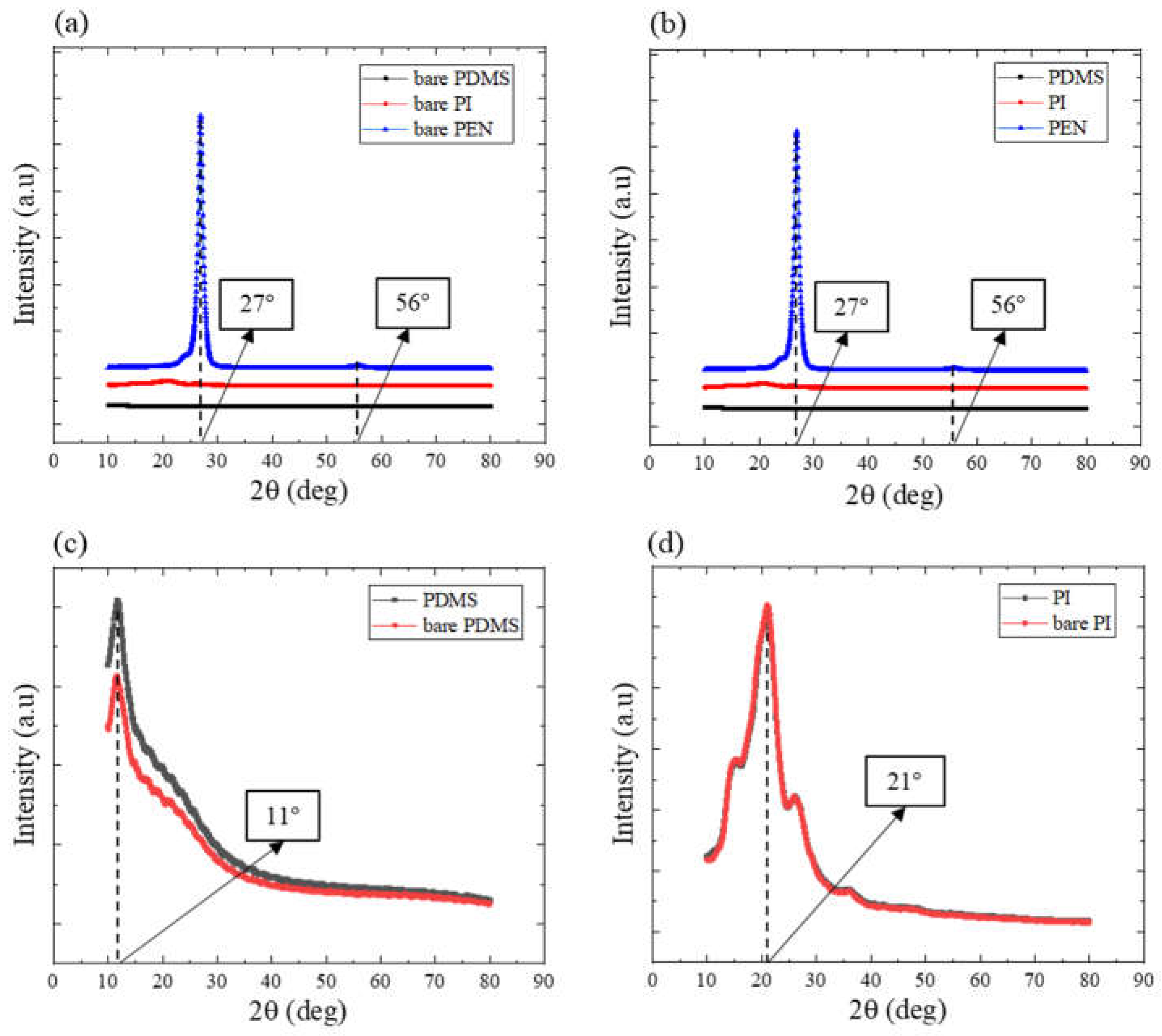
Figure 4.
For four different substrates, the M-H loops are showed with in-plane magnetic field (black line) and out-of-plane magnetic field (red line) for each sample (a) Si/SiO2, (b) PDMS, (c) PI, and (d) PEN.
Figure 4.
For four different substrates, the M-H loops are showed with in-plane magnetic field (black line) and out-of-plane magnetic field (red line) for each sample (a) Si/SiO2, (b) PDMS, (c) PI, and (d) PEN.
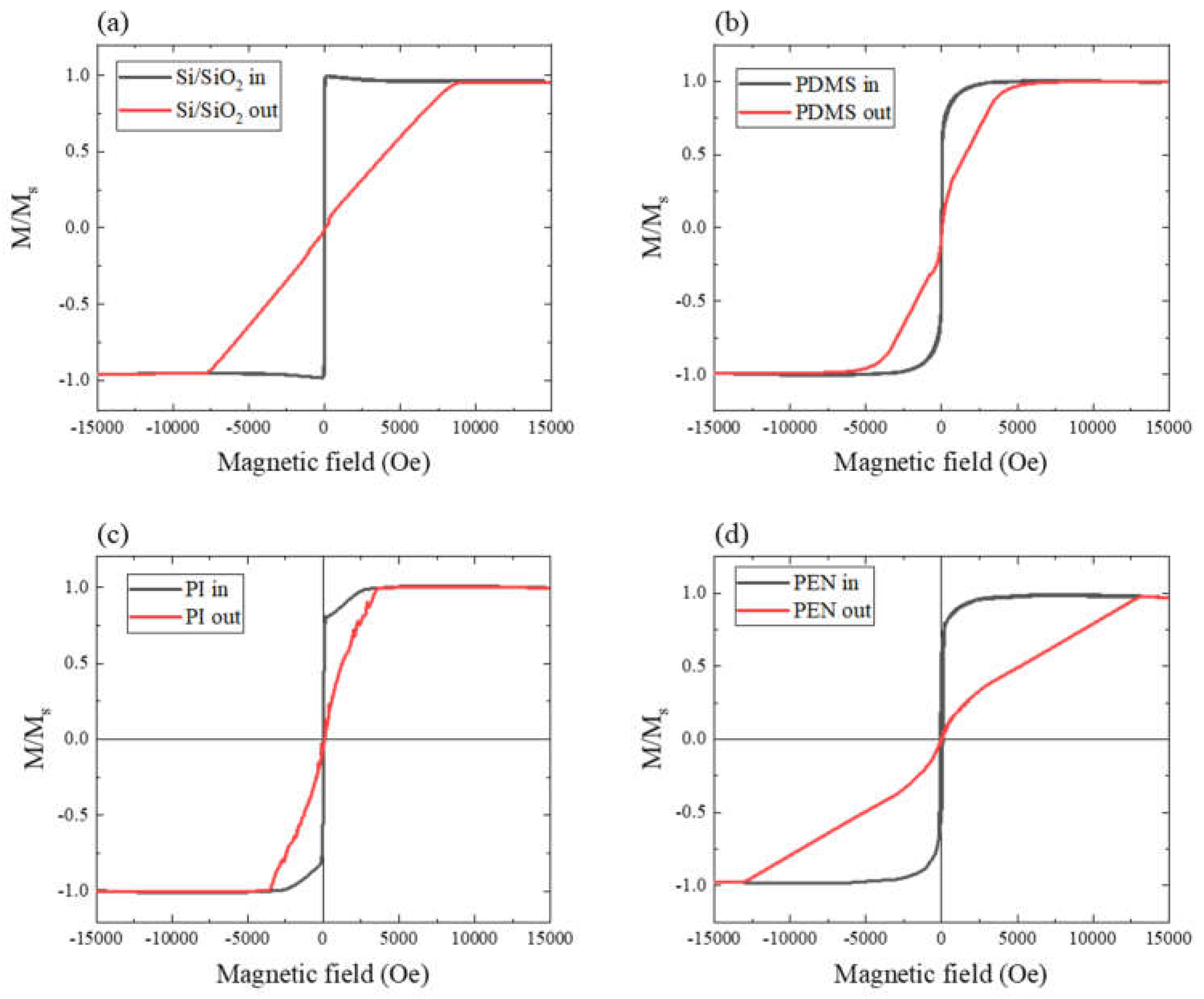
Figure 5.
For four different substrates, (a,c) M-H loops of the samples on in-plane magnetic field of 0° and 90°, respectively; (b,d) Hc of the samples vs surface roughness (Rq) of substrates for 0° and 90°, respectively; (d) Rq of the four substrates (Si/SiO2, PDMS, PI and PEN).
Figure 5.
For four different substrates, (a,c) M-H loops of the samples on in-plane magnetic field of 0° and 90°, respectively; (b,d) Hc of the samples vs surface roughness (Rq) of substrates for 0° and 90°, respectively; (d) Rq of the four substrates (Si/SiO2, PDMS, PI and PEN).
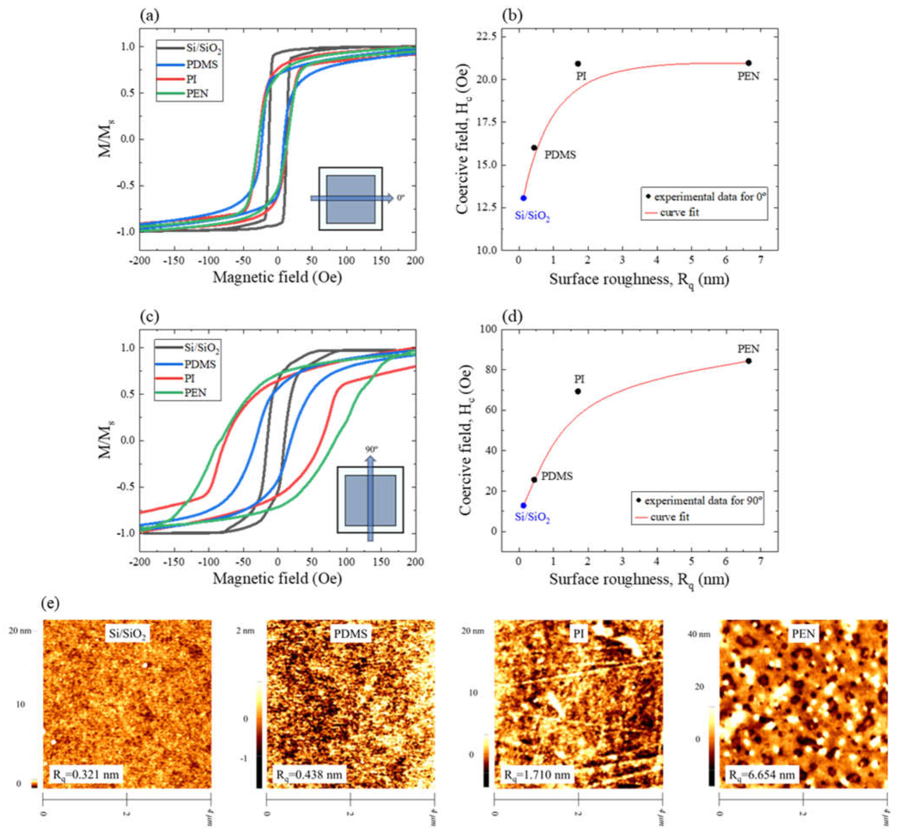
Figure 8.
Measured before, with, and after applying the tensile strain, (a) M–H loops; (b) histograms of the MFM phase; (c) MFM phase maps of the PDMS samples.
Figure 8.
Measured before, with, and after applying the tensile strain, (a) M–H loops; (b) histograms of the MFM phase; (c) MFM phase maps of the PDMS samples.
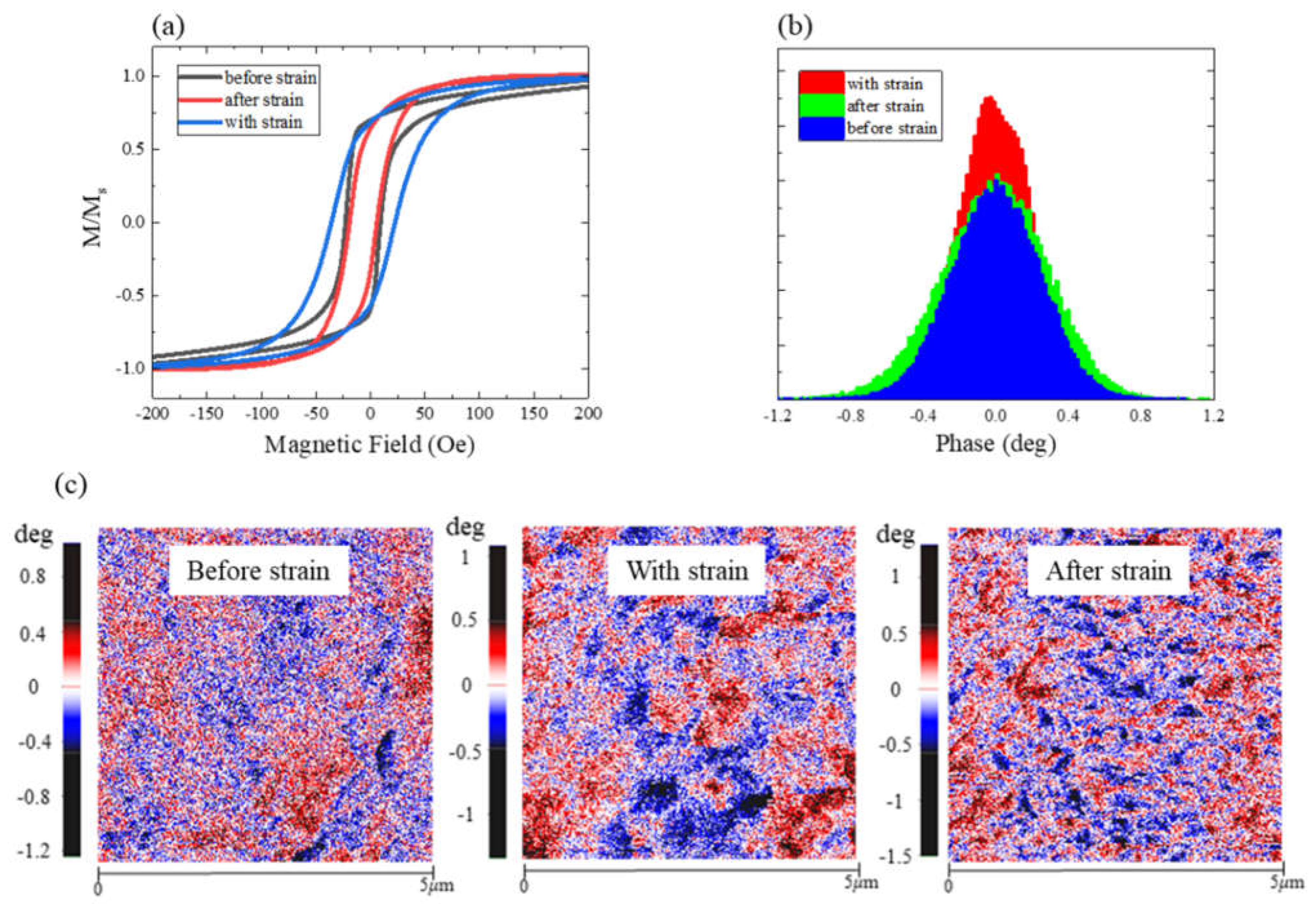
Table 1.
Rq, Hc, and Mr/Ms with substrates at 0° and 90°.
| Substrate | Rq, nm | Hc, Oe | Mr/Ms | ||
|---|---|---|---|---|---|
| 0° | 90° | 0° | 90° | ||
| Si/SiO2 | 0.13 | 13.06 | 12.65 | 0.93 | 0.59 |
| PDMS | 0.44 | 16.01 | 25.66 | 0.70 | 0.03 |
| PI | 1.71 | 20.92 | 69.30 | 0.76 | 0.18 |
| PEN | 6.65 | 20.96 | 84.35 | 0.69 | 0.62 |
Disclaimer/Publisher’s Note: The statements, opinions and data contained in all publications are solely those of the individual author(s) and contributor(s) and not of MDPI and/or the editor(s). MDPI and/or the editor(s) disclaim responsibility for any injury to people or property resulting from any ideas, methods, instructions or products referred to in the content. |
© 2023 by the authors. Licensee MDPI, Basel, Switzerland. This article is an open access article distributed under the terms and conditions of the Creative Commons Attribution (CC BY) license (http://creativecommons.org/licenses/by/4.0/).
Copyright: This open access article is published under a Creative Commons CC BY 4.0 license, which permit the free download, distribution, and reuse, provided that the author and preprint are cited in any reuse.


