Preprint
Article
A/D Conversion with Oversample and Average Based Precision Improvement
Altmetrics
Downloads
198
Views
48
Comments
0
This version is not peer-reviewed
Submitted:
21 June 2023
Posted:
21 June 2023
You are already at the latest version
Alerts
Abstract
This paper presents high-resolution digital measurements at low cost, combining oversample and averaging. Experiments of processing data between samples and between multiple temperature sensors in the same environment are conducted. They provide results with effective increase in the analog to digital converter bits, in correspondence with the minimization on the effects of noise. It is shown that averaging a set of small, low-cost sensors at a small microcontroller can give flexible access to improved measurement accuracy.
Keywords:
Subject: Engineering - Electrical and Electronic Engineering
1. Introduction
Considering the high costs of industrial and military classification sensor systems containing “precision” electronics, this work attends to alternative methods that may be sufficient in several applications. The aim is to improve the parameters of the desired final “precision”, with some options to make the result more flexible.
It is presented the use of eight temperature sensors of the same model, measuring the same ambient temperature, to average the set, associated with the automated oversample resources of a microcontroller [1]. The performance of this oversample is compared with the equivalent procedure in software (C language/ microcontroller). Starting from Analogue-to-Digital (A/D) conversion results, the standard resolution is increased by using oversample and noise is minimized also by averaging between sensors. Low-cost temperature sensors and reduced dimensions are used, criteria also followed in the choice of computational platform.
One characteristic of sensors that was not considered in this study is the linearity, nor of the chosen sensor [2], nor of the A/D converter, since attention to noise was related to the increase in the number of bits of measurements [3]. Likewise, offset errors are disregarded here, despite being known to be increased when using the oversample [3]. They can be easily evaluated with measurements made with short circuit in the analog inputs and compensated in modern microcontrollers by simple configuration of internal registers (individual adjustments in Programmable Gain Amplifiers [1]).
The delimitation of the practical uses of this work correspond to those cases in which the studied physical quantities are characterized by very slow variations in relation to the sampling rate, enough to consider the signals as stationary. It is a criterion assumed to be true for the ambient temperature, but it can become critical in case of relating small thermal variations with other physical phenomena, so this stationarity must be studied. Examples of slowly varying quantities: measurements of temperature, sulfuric acid density in stationary batteries, salinity and current at the bottom of the sea. Regarding the use of multiple sensors, he is inspired by the sensation of cold, which results from the average of many sensors per skin area, with distributions in different densities in each part of the body (biological plausibility).
The paper is organized in sequential topics. The quantization process is described, the topologies and performances of analog-to-digital converters are detailed, the electronic platform is presented according to choosing criteria, and the results are exposed in graphics and interpretations.
2. Overview of Analog-to-Digital Conversion
Digital processing of sensor signals requires prior quantization at discrete time. Using analog-to-digital converters, some continuous signal variations in time become represented as a finite sequence of words consisting of 8 to 32 bits (1s and 0s) usually. Signals such as the internal pressure of a vessel or rapid air pressure variations related to of sound waves are converted by a transducer to a proportional analog electrical signal. The number of digital levels used to represent each analog signal sample and the rate at which it is converted is a function of the desired accuracy. These parameters together change the cost of the system. In this section the quantization process is described, and the performance of an analog-to-digital converter are detailed.
2.1. A/D Converter Specifications
The analog signal can be a voltage signal as shown at Figure 1 horizontal axis, being FS the analog full-scale level. The evolution in steps corresponds to the ideal transfer function for a 3-bit A/D conversion. The output of the converter can be generalized as an n-bit digital code given as,
where Asig is the analog signal and bn is a digital value of either 0 or 1. As shown in the figure, each digital code represents an interval of analog levels. The interval corresponds to the least-significant bit (LSB) and one step cross the center of each quantized region.
The sensibility of a converter is the smallest change at an analog input for an A/D converter to result on a distinct digital code. This can be expressed as
also indicating the smallest analog signal for an N-bit conversion. The accuracy of a converter, often referred to as relative accuracy, is the worst-case error of the actual converter output relative to the ideal output, after removing gain and offset errors. This is quantified as the ENOB (equivalent number of bits) or as a fraction of the LSB.
The conversion rate is related to “how fast” a digital code is accurately generated from a sample of an analog signal. This is often an underlying factor in choosing the converter architecture. Sampling and holding (in separate channels) multiple times sequentially from the same analog signal and converting each one with a separate A/D converter can be done to allow higher speeds above some architecture limits. This is the opposite from the proposed in this paper. Here the aim is to increase the announced precision, oversampling and averaging multiple channels, with the penalty of lower conversion speeds.
Nonideal A/D and D/A Converters
Actual A/D converters exhibit deviations from the ideal transfer function. Device parameters such as voltage thresholds, spurious capacitances and inductances (changing time delays in signal paths), internally generated noise, can manifest themselves into these deviations. Glitches on analog paths can occur during changes in the digital output transitions. Many other circuit parameters can cause a change (in bits) of the resulting code.
Static errors are well defined at literature and shown on datasheets for the commercial models. Some of the most important are Offset error, Gain error, Integral nonlinearity, Differential nonlinearity.
Dynamic performance parameters include information about noise, dynamic linearity, distortion, settling time errors, and sampling time uncertainty of an A/D converter. The following measures are both frequency and amplitude dependent.
Signal-to-Noise Ratio
The quantization process introduces this kind of dynamic error, which sets an irreversible limit for the dynamic range. If the quantization error of an A/D Converter is evenly distributed, the theoretical power of the generated noise can be evaluated by:
where VLSB is the quantization step [5]. If a pure sine wave signal with a maximum amplitude is presented to an ADC with a number of bits greater than 5, the signal rms power is evaluated by:
The Signal-to-Noise Ratio (SNR) for this pure sinusoidal signal is:
The ratio between the frequency of the sine wave and the sample rate fS should be irrational. If the input signal deviates from the sine wave, the constant term, which depends on the amplitude rms value of the waveform, differs from 1.76 dB. Equation (5) indicates that each additional bit, N, gives an enhancement of 6.02 dB to the SNR.
If oversampling is used, which means that the sampling frequency is much larger than the signal bandwidth fsig, the quantization noise must be averaged over a larger bandwidth and the SNR will be larger:
where the oversampling ratio OSR is given by
In cases attending to the Nyquist rate, the signal bandwidth is fS/2 resulting in an OSR equal to one, and equation (6) suggests that the signal-to-noise ratio increases by 3 dB per octave of oversampling.
Total Harmonic Distortion
Any nonlinearity in an ADC generates harmonic distortion. Total Harmonic Distortion (THD) is the degradation of the signal-to-distortion ratio caused by the harmonic distortion, expressed with
where NH is the number of harmonics to be considered, V(fsig) and the amplitude of the fundamental and the jth harmonic, respectively.
Effective Number of Bits
In ideal A/D converter systems, the maximum analog bandwidth is related to the number of the bits for a single-tone full-scale sinusoidal test signal is called the Effective Number Of Bits (ENOB)
where (SNDR or SINAD) is the signal-to-noise and distortion ratio, in which the total error energy includes all spurs and harmonics. For static analysis, this ENOB is a reference for the required class of precision used to choose the components surrounding the ADC. If the chosen ADC model has a series of good qualifications, then the other components could follow them and make some advantage. All the parts of some circuit will be chosen to be compatible with (better than) the ENOB reference, even if ADC have exciding qualifications.
2.2. A/D Converter Architectures
Conventional converters work by sampling the time varying analog signal at a sufficient rate to fully resolve the highest frequency components. According to the sampling theorem, the sampling rate must be over twice the frequency of the highest frequency contained in the signal source. Certain architectures exploit parallelism to achieve high speed operation on the order of 100’s of MHz, and others which can be used for high accuracy 16-bit resolution for signals with frequencies on the order of kHz.
Flash A/D
With the flash A/D, the highest speeds are reached when maximum parallelism is used. It requires 2n − 1 analog comparators, 2n − 1 reference voltages, and a digital encoder. For a linear scale, the reference voltages are required to be equally spaced between 0.5 LSB above the minimum signal and 1.5 LSB below the maximum signal and spaced 1 LSB apart. The results at the output of the comparators are already digital but require to be converted to binary to save digital signal paths on circuit board (2n levels became n bits, ex. 256 to 8). The speed of the converter is limited by the time delay through a comparator and the binary encoding logic. This speed is gained at the expense of accuracy. It is expensive to produce equally spaced reference voltages and precision comparators.
Successive Approximation A/D Converter
A successive approximation A/D converter [5] is formed by a circuit that artificially generates a very specific sequence of analog signals, following the known sequence of a binary tree. To verify the path to follow through the tree, a feedback loop is built around a D/A converter and a comparator. A successive approximation register (SAR) is initialized to a value where all bits are set to 0 except the MSB which is set to 1. This represents the mid-level digital value. This value is fed to the D/A converter and the resulting mid-level analog value goes to the comparator, used to determine whether the mid-level generated analog signal is greater or less than the input (sensor) analog signal. The control logic determines whether to leave the MSB set to 1 or to change it back to 0 (if the addition of middle value was excessive). On the next clock cycle, the next MSB is tested (set, compare, reset if the addition of a quarter was excessive). The process is repeated by “n” clock cycles for an n-bit converter. By this sequence, a half of the last try is added, and then, all the bits are required to fine approximate and fully quantize the sampled instantaneous analog signal. The speed of the successive approximation converter is limited by the delays of the DAC and the comparator. This converter is used for medium speed and the resolution is related to the DAC converter and the comparator.
Pipelined A/D Converter
In a pipelined A/D converter the conversion process is broken into multiple stages. Each stage does a partial conversion, and the converted bits are shifted by digital registers. The outputs of the ADC are connected directly to a DAC and is subtracted from the original analog signal to get a residual signal. This signal is then amplified by 2n to fit in the entire full-scale of the next stage. On the next clock cycle the first stage begins conversion on the next analog sample while the second stage refines the conversion already in process. The limit on the conversion speed is related with the delay of a single stage. Pipelining allows high resolution conversion using a relatively small number of comparators. An 8-bit converter can be constructed with 4 stages with 2 bits per stage, requiring only 12 comparators. With an 8-bit flash converter requires 255 of them. Each pipeline stage adds an additional latency for the final conversion. A pipelined A/D converter achieves high-speed conversion and high accuracy, but the conversion latency can be an impeditive in the process.
Delta-Sigma Oversampling Converter
The delta-sigma ADC is chosen when cost must be kept at a minimum [2]. It exhibits high-resolution when become difficult to realize high resolution conversions by Nyquist rate converter architecture. These oversampling converters use cheap analog components at the front end and digital signal processing in the later stages. An oversampled delta-sigma A/D converter is sampled at a higher rate than the input Nyquist rate. A simple first-order lowpass filter is used to attenuate the noise to avoid the noise aliasing. The noise components are close to the sampling frequency and then will be aliased back into the signal band. This arrangement simplifies the necessary filter. The A/D itself is simpler than the non-sampled A/D converters.
State of the art
The actual state of the art about the utilization of ADC is different from the academic initiatives. To use some ADC in measurement topology research, the best choices must be sought in the datasheets of the silicon industry. Commercial devices available in market are usually based on solid configuration strategies, to get high level of accuracy. At [5] is possible to find a table with data to compare the commercial devices available at the time of publication. The author also includes then some data collected on articles of important conferences and journals in a graphic to make a good comparison between different typology of converters and get perspective of the future.
The most important specifications of any ADC are the signal bandwidth, BW, and the ENOB. To find state of the art in commercial areas of dynamic research, like applications on mobile communication [6], the selection of fundamental criteria can be very specific. For a sake of exemplification, the conversion to digital in Software-Defined Radio (SDR) includes a low pass filter taking place of the oversample circuit (LP-SDM) to be compared with the innovative band pass (BP-SDM). The notch frequency of the band pass filter, fn, should be well evaluated since it would affect the amount of energy (power) needed to digitize a signal. Regardless of the architecture and circuit technique used [6], BP-SDMs are not competitive yet with their LP-SDM counterparts, which explains why direct-conversion receiver is yet in use in mobile terminals, even though they are sensitive to analog impairments of I/Q down conversion. To make BP-SDMs more efficient for RF ADCs in SDR, it is needed to adopt circuit techniques which can increase the carrier (notch) frequency programmability, with reduced power consumption and lower (analog) hardware complexity [7].
If the “low complexity” is the main rule, at this time of increasing digital performance, low-accuracy analog components can be used, assisted by digital correction or calibration, which leads to a reduction in power dissipation [7]. One strong trend in the design of analog-to-digital converters has been to use low-accuracy analog components assisted by the powerful digital logic to calibrate the circuit behavior and increase the performance while reducing both power dissipation. There are lots of published analog-to-digital converters following the trends to reduce the power dissipation every year. Thermal noise set a lower limit on the power dissipation. The support of digital logic can be used to estimate the gain errors, which can then be trimmed by analog circuitry, removing the need for the additional power dissipation of the correction digital logic. The use of redundancy is taken one step further in a 1.5 GS/s 90nm flash ADC where the reference network is removed.
3. System Platform
Before entering noise studies and their relationship with measurement resolution, it is necessary to choose the electronic platform that allows testing and accumulating results in files for post-processing and studies.
The first choice to be made in low-cost solutions is the most expensive component, the microcontroller, which performs sample acquisition and the automated “oversample”. If we consider the types of microcontrollers with easy prototyping (small development kits), those compatible with the Arduino standard [ref] are known for their wide availability around the world, at the time of the experiments conducted for this work. Among these only a few types have an extra number of analogue inputs (8 or 16, to study the advantages of averaging between them, in conjunction with increased resolution in effective bits). For comparison, the most popular “Arduinos” only have 6 inputs. There are also few that have the feature of automating the averages or sums of successive measurements.
A comparative study was carried out between models available on the market, with different cost ranges, physical dimensions, and sampling rates. Compatibility with serial communication (USB) was also chosen as a criterion to allow the recording of data sequences in disk files using standardized libraries of free use in Python language. With such criteria, these are the models to choose from:
ESP32 [8]
Arduino Pro Mini 33 [8]
Xiao SAMD21 [1]
Xiao nRF52840 (includes Wi-Fi) [9]
SAMD21 M0-Mini [1]
Some of these on the list appear in discussions (forums) on the Internet because they have noisy analog inputs, with no hardware solution indicated. The fact that one or another model contains integrated radio transmission (Wi-Fi, Bluetooth) already presents some foreseeable disadvantages in this aspect.
With a price much lower than the others (in all the local stores surveyed) and small dimensions, the choice was for the third, with a 32-bit ARM M0 microcontroller [1] from Microchip, the ATSAMD21G18A-MU. It is available on Seeeduino Xiao SAMD21 development boards likely intended to be integrated into projects, as it is marketed, Given its dimensions and the prices set, it seems that they would have to compensate for the engineering costs of this portion of the microcontroller.
The chosen development board is among the products that make design concessions to achieve its reduced size. One such compromise is that the analog voltage supply (VddAna) is connected directly to the digital supply pins (VddIOx) thus omitting the recommended ferrite filtering in the SAMD21 datasheet [1]. Noise generated by rapid digital level transitions ends up interfering with analog inputs. The board also does not offer the possibility to use an external precision voltage reference, as the pin (Aref) is not easily accessible.
Figure 2.
Circuit assembly showing 8 NTCs and 10 kΩ resistors in typical voltage dividers.
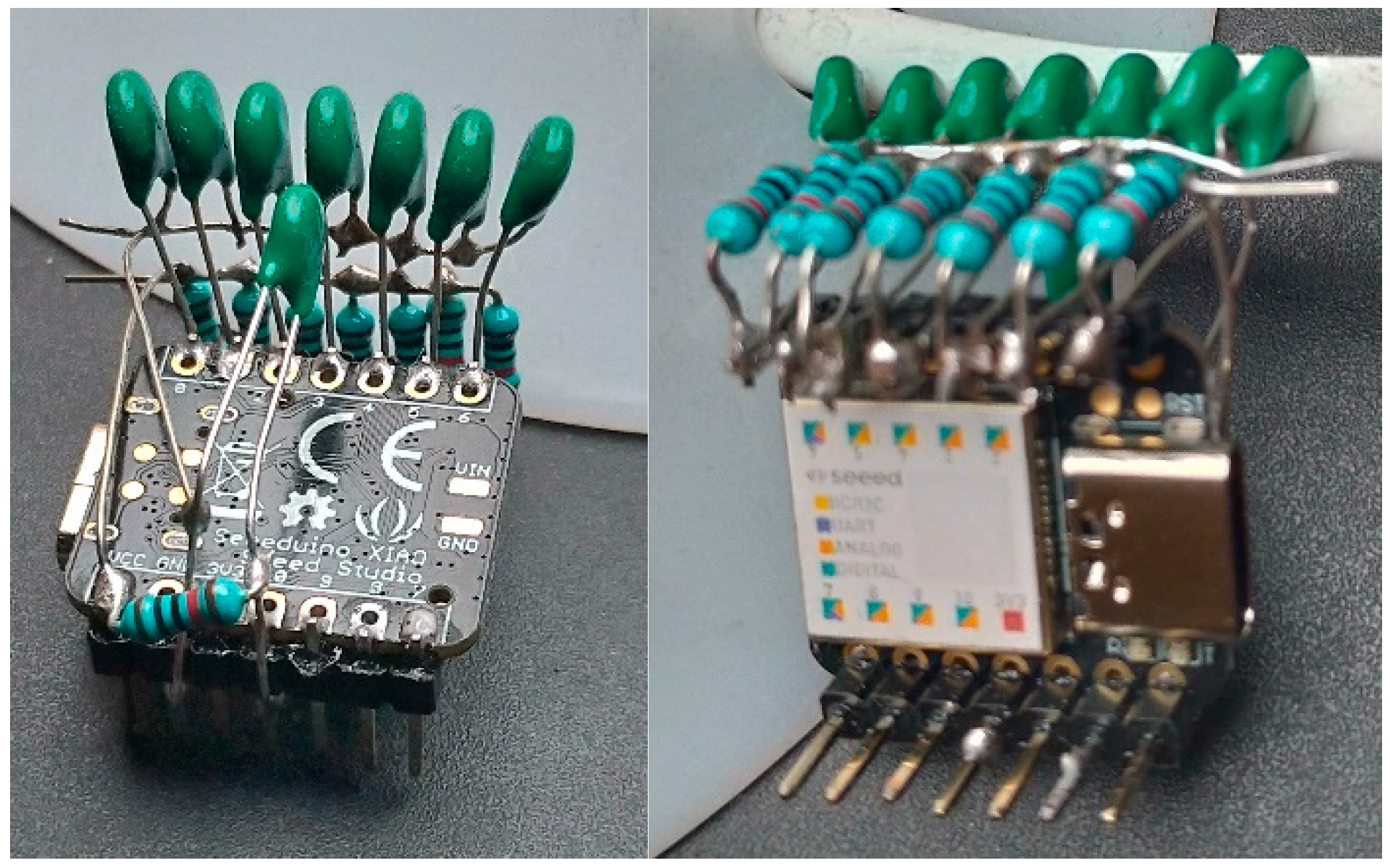
Alternatives could be sought in terms of current microcontrollers on the market. Some of them could be very expensive, but justified by other criteria like available wireless communication, internet access, and those best served by resources with hardware choices (choices via registers, bit fields).
3.1. Noise and Resolution
Precision measurements require the use of circuit design techniques such as differential inputs [2], pre-amplification with balanced topologies, industrial (or even military) precision grade components with low noise specifications [ref], shielded sensors to reduce radiated electromagnetic interference. All of this corresponds to high costs for each component, see equation (15) and they are completed with assemblies on multilayer printed circuit boards with separation of power supply circuits from the analogue portion, at least by positioning LC filters up to the digital power points.
The references containing theoretical bases on the effectiveness of the oversample in increasing conversion bits [4] advocate the need for Gaussian noise added to the analog signal, therefore, what is often a problem, can be a solution in this case. There was no concern here to verify whether such noise conditions complied with the limits of these conditions, as the resulting noise in all variations (first tests) reached the same minimum percentage error, below +/- 1 LSB.
3.2. Temperature sensors
Among the various types of temperature sensors, in the range of -50°C to +150°C, NTC type thermistors provide a good combination of sensitivity, cost and simplicity of use. The choice for other types (thermocouples, PT100, Bandgap) and the circuit topology depends not only on the temperature range being measured, but also on the required precision [10,11]. NTCs are non-linear and require the use of compensating circuits or some linearization algorithm (if it is a microprocessor system), necessary to achieve accurate temperature values.
Figure 3.
Response Characteristics of a 10 kΩ NTC (adapted from [5]).
Figure 3.
Response Characteristics of a 10 kΩ NTC (adapted from [5]).
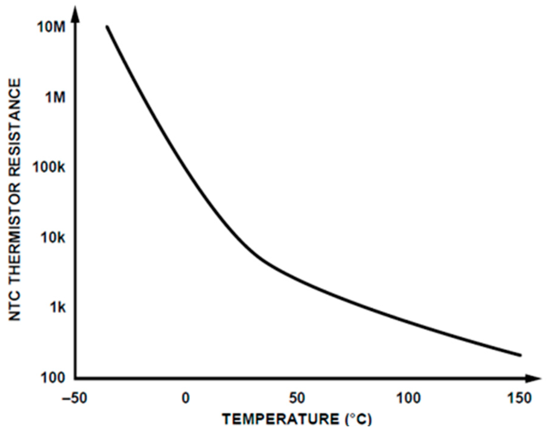
The resistance of NTC thermistors decreases as temperature increases. The Steinhart-Hart equation is an empirical expression that was determined to be the best mathematical expression to use to correct the nonlinear response (resistance vs. temperature characteristics) of typical NTC thermistors.
The Steinhart-Hart equation for temperature as a function of resistance follows:
where,
- T is the temperature in degrees Kelvin.
- A, B, and C are the constants derived from the three temperature test points.
- RTH is the resistance in ohms of the thermistor.
The values of A, B, and C are dependent on the specific thermistor model, which can be found in the selected thermistor data sheet. If the data sheet gives A, B, and C, this equation can be used directly to calculate the temperature as a function of the measured resistance. Some NTC thermistor manufacturers do not provide the values for the A, B, and C constants. Instead, the thermistor is specified with a single beta (β) constant representing a change in resistance, calculated using the resistance value at two specified temperatures [5].
where,
- R is the resistance in ohms of the thermistor.
- β is a constant representing a change in resistance.
- T is the temperatures in Kelvins.
- T0 = (25°C = 298.15 K).
- is the resistance at temperature T0.
It must be written a simple program that reads the thermistor’s voltage at the voltage divider, converts it to a resistance, then using the Steinhart-Hart equation, converts the resistance across the sensor to a temperature in degrees Celsius. The resistance across the sensor and the computed temperature are then returned to the connected personal computer.
The criterion of choosing temperature sensors with small dimensions aims to minimize the total cost, as well as to minimize the factors that lead to the capture of interference, since short connections expose less of the circuit to electromagnetic waves. A CNT of small dimensions and very low cost was sought.
3.3. Oversample procedure
The Oversample procedure consists of making successive sums of the direct output read at the A/D converter (12 bits, in the chosen microcontroller), each sum resulting in the occupation of 1 more bit. Therefore, it is possible so far to get additional 4 bits after adding 4 times, those 12-bit words. With these 16 bits, the first evaluations of mean and standard deviation were made, for each sensor, to compare with the following deeper oversample/averages. Other comparison was made, calculating a moving average of sequences of eight samples (for 1 sensor), confronting with the average between the 8 sensors. It is well known [12] that oversampling the ADC by a factor of four results in some measuring errors (like the increase of gain in analog circuits). Therefore, it provides just one additional bit of resolution at the same error measurement class. It is the same of getting 6 dB increase in Dynamic Range.
Sequence of operations for the implemented Oversample:

Simple code in C language for the implemented Oversample:
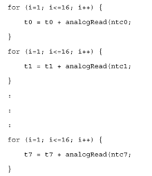
To achieve results comparable to what the microcontroller datasheet promises, this sequence of four sums was continued by other four similar stages, but always preceded by divisions by two (configuring then average calculations), dropping to 15 bits and returning to 16 after each sum. Thus, there is no occupation of one more bit at each step, keeping the result in 16 bits. With these 16 bits containing the oversample/average of 256 results from the 12-bit A/D converter, the next mean and standard deviation evaluations were made, also for separate sensors, (making moving average in sequences of eight samples), comparing with mean between the 8 sensors.
Sequence of operations for the Averages that follow Oversample, to keep the 16-bit result.

Simple code in C language for the implemented Oversample to keep the 16-bit results:
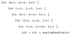
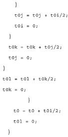
Note that in the innermost loop - i - there is counting up to 16, always doing simple sums - oversample - and in the other loops up to the outermost - j,k,l,m - division by 2 occurs before adding the value that the last oversample resulted. Finally, the oversample/automated average is repeated using internal registers, following the guidelines of the microcontroller datasheet, and repeating the statistical calculations.
4. Results
Four sequences of experiments were conducted for comparison, with uniformity in the questions: bit count increased by oversample, from 12 to 16 bits and relative calibration between sensors using average between them after oversample increasing to 16 bits.
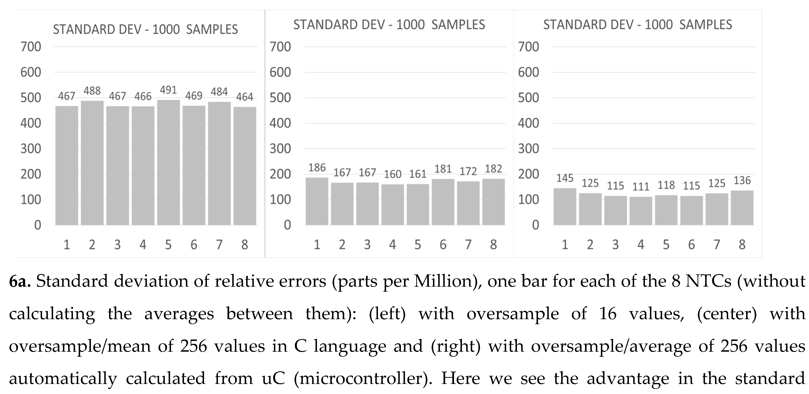
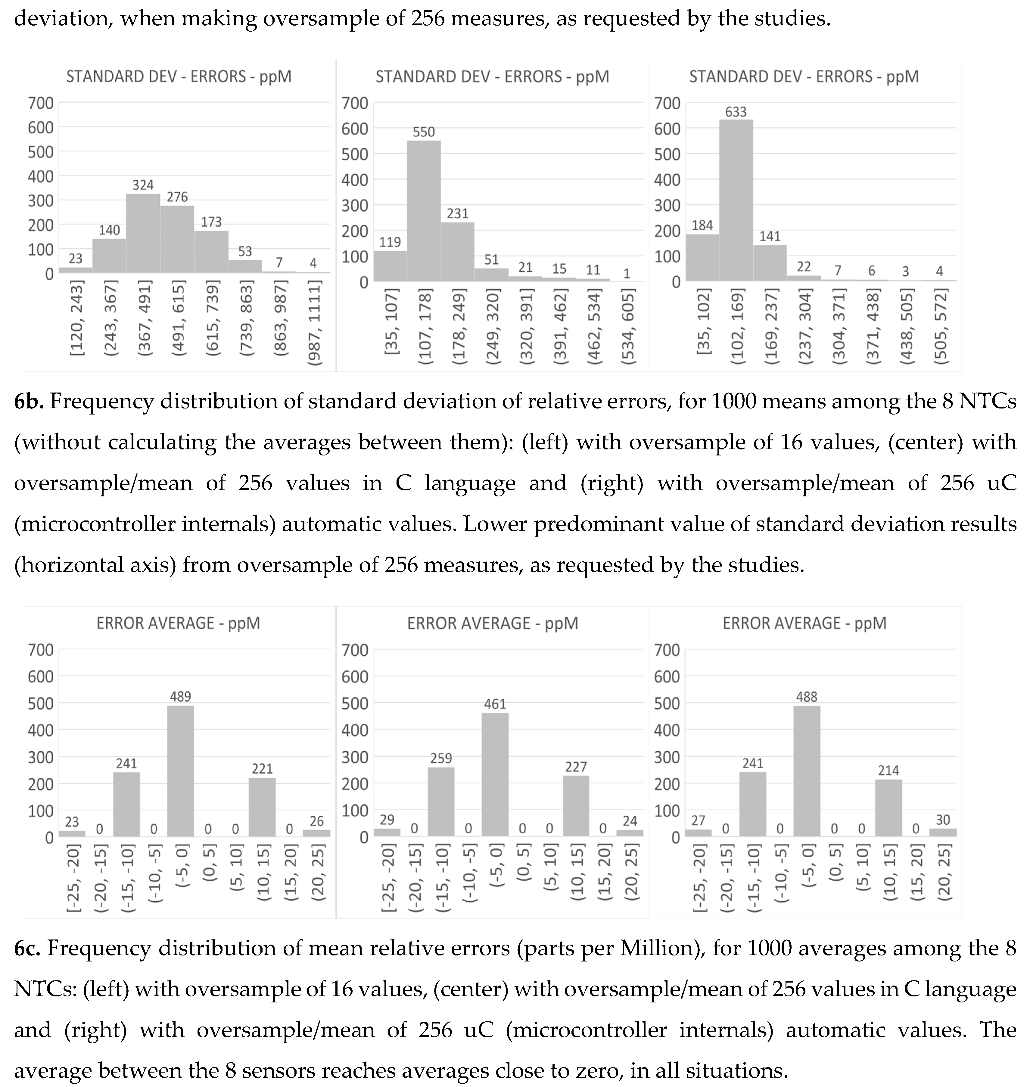
The settings of the A/D converter are made, for the use of automatic oversample or not, for the use of automatic average or not. When only the oversample is done, the sequential summation of 16 samples is performed. For every two data that are added, 1 bit is gained. So, starting with the 12-bit A/D converter outputs, after 4 2-in-2 combinations, it results in 16 bits. If the oversample is followed by averages, each sample is previously divided by two so as not to exceed 16 bits. The error relative to the average between the eight sensors (x100, percent) is calculated. This code put values available on serial interface, which will be read in Python, every 10 seconds, 1000 times. Using Python for serial reading, writing in txt file, lines with 8 percentage errors each and a temperature measurement (average); Excel imported part of the CSV file, evaluate mean and standard deviation between sensors and standard deviation in 1000 samples (1 sequence dismissed, because average order doesn’t care). Cluster averages across the eight sensors are also computed with the individual moving averages of two sensors (using the last eight samples over time). All these measurements are repeated in the three oversample methods, for comparison.
The scales with maximums of 500 ppM in the first (16 values), 250 ppM in the next two, above (due to the oversample with more values, 256), the first was doubled so that the three show, in same size, final errors averaged across sensors (black).
5. Conclusions
The contribution of this work lies primarily in the remarkable usefulness of the average between channels, not implemented in most of the related works. Since the first results, it is confirmed that it is possible to use it as a reference in this paper, dispensing the comparison with traceable measurements, in well-equipped laboratories.
To compensate, as much as possible, the sensitivity imbalances between channels (relative calibration), calibration coefficients are calculated for each individual sensor, using as reference the average between the 8 sensors, since the first tests. The effectiveness of this procedure is confirmed in all the results obtained (mean errors below 1 LSB). Before each batch of measurements is recorded in a file, the oversample of at least 16 measurements of each sensor is obtained and divided by this reference to obtain the individual calibration factor. Then, in the collection of 1000 measurements, each one of them is calibrated and its error relative to a new mean (between the already calibrated sensors) is calculated. Finally, a generated file contains 1000 relative error values for each individual sensor.
In practice, adjustments (calibrations) of individual gains can be automated using amplifiers internal to the microcontroller, with programmable (analog) gains in (digital) registers. Despite being available on the microcontroller used for the experiments (PGA - SAMD21 [1]), this proved to be out of context for the proposed approach, as the calibration was developed in an integrated manner with the non-automated oversample/average algorithms. Such solutions fit within the chosen components, justifying their use if the technical solution is referred to a technological solution (commercial product).
The flexibility mentioned in the objectives includes the choice of the number of sensors, the number of bits added by the oversample/average procedures, the possibility of using a simpler microcontroller (without oversample/average, internal, automated), obtaining approximate results by programming (nested loops, performing the same operations), despite losing performance in bandwidth.
Achievable higher precision with low cost depends on integrating oversampling into microelectronics, although being restricted to slower problems. In those case, the costs of "precision analogue" can be avoided.
Even lower cost is achievable if you do oversample/average using smaller adders, as the differences between the values appear only in the least significant bits (possibly as a continuation of this paper) This type of study, close to everyday observations, motivates beginners in scientific research, favoring the choice of components and programming languages among the most popular ones.
References
- Atmel-42181J-SAM D21, 2023 datasheet – access in (https://files.seeedstudio.com/wiki/Seeeduino-Cortex-M0-/res/SAM-D21-Datasheet.pdf).
- CN0545 Completely Integrated, 0.1°C Thermistor Measurement System Using a Low Power, Precision, 24-Bit Sigma-Delta ADC – access in (https://www.analog.com/en/design-center/reference-designs/circuits-from-the-lab/cn0545.html#rd-functionbenefits).
- Application Note - Noise_an118.pdf - Improving Adc Resolution By Oversampling And Averaging, Silicon Laboratories, 2013 Rev. 1.3 – access in (https://www.silabs.com/documents/public/application-notes/an118.pdf).
- Galton I, Jensen, H., Oversampling Parallel Delta-Sigma Modulator A/D Conversion, IEEE Transactions On Circuits and Systems -II Analog and Digital Signal Processing Vol.43, N0.12, December 1996.
- Agnes A., Low Power SAR ADC Instrumentation, Tesi di Dottorato, Universitá Degli Studi di Pavia, September 2008.
- de la Rosa, J.M. Bandpass Sigma–Delta Modulation: The Path toward RF-to-Digital Conversion in Software-Defined Radio. Chips 2023, 2, 44–69 – access in (https://doi.org/10.3390/chips2010004). [CrossRef]
- Jin, Le & Parthasarathy, Kumar & Kuyel, Turker & Chen, Degang & Geiger, Randall. (2005). Accurate Testing of Analog-to-Digital Converters Using Low Linearity Signals With Stimulus Error Identification and Removal. Instrumentation and Measurement, IEEE Transactions on. 54. 1188 - 1199. 10.1109/TIM.2005.847240. [CrossRef]
- Arduino Home Page – boards – access in (https://www.arduino.cc/en/hardware#boards).
- Nordic Semiconductors - nRF52840 datasheet – access in (https://files.seeedstudio.com/wiki/XIAO-BLE/Nano_BLE_MCU-nRF52840_PS_v1.1.pdf.
- McGee, T. D. Principles and Methods of Temperature Measurement, John Wiley & Sons, 1988.
- Jones, D. P., Biomedical Sensors, Momentum Press, 2010.
- AN-1279 Application Note, Oversample 5 MSPS 16-Bit Precision SAR.
Figure 1.
Ideal Transfer Characteristics for A/D Converter (adapted from[4]).
Figure 1.
Ideal Transfer Characteristics for A/D Converter (adapted from[4]).
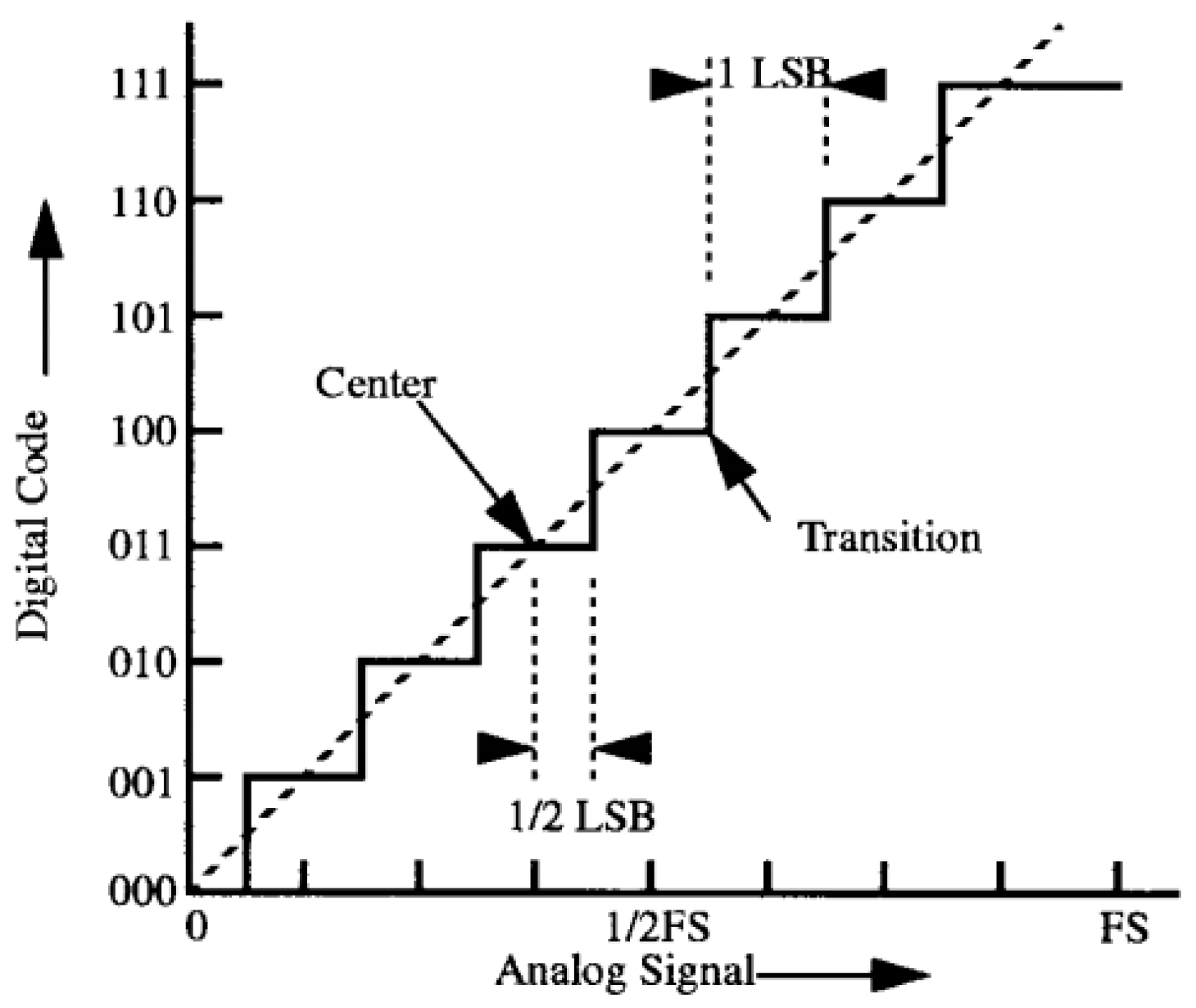
Figure 4.
Sequences of 200 values of moving averages with a,b,c proposed post-processing methods.
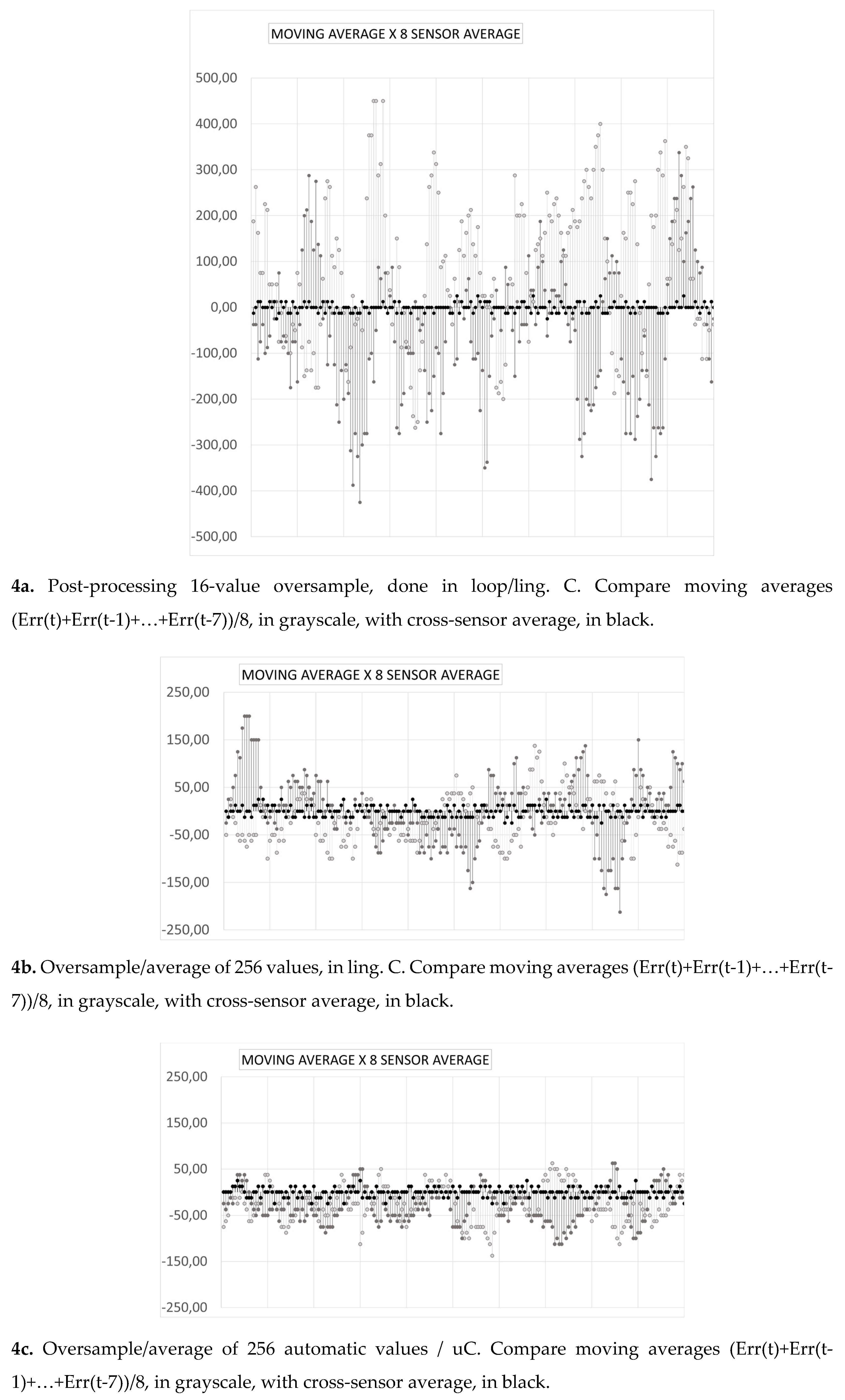
Figure 5.
Sequences of all 1000 values of 8 NTCs with the proposed a,b,c post-processing methods.
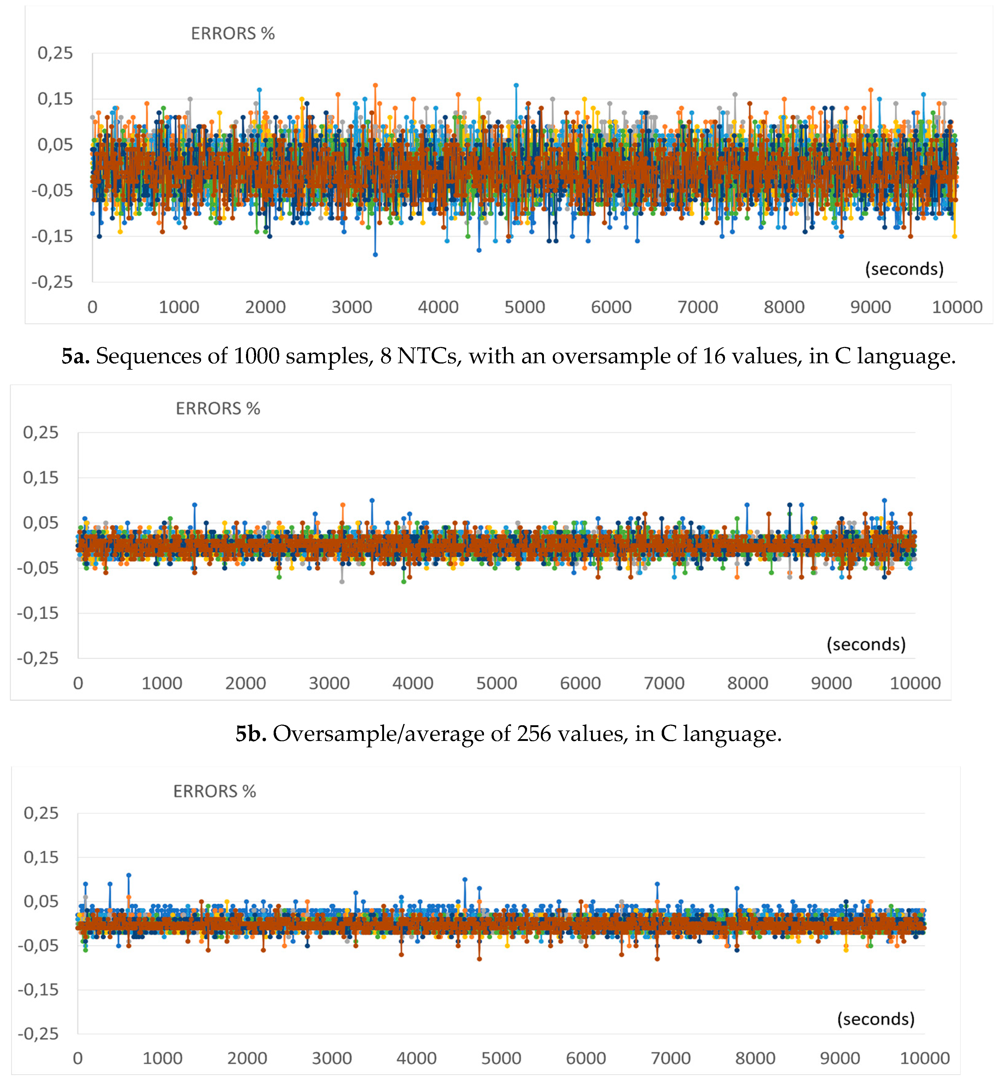
Figure 6.
Statistical results showing differences between proposed a,b,c post-processing methods.
Disclaimer/Publisher’s Note: The statements, opinions and data contained in all publications are solely those of the individual author(s) and contributor(s) and not of MDPI and/or the editor(s). MDPI and/or the editor(s) disclaim responsibility for any injury to people or property resulting from any ideas, methods, instructions or products referred to in the content. |
© 2023 by the authors. Licensee MDPI, Basel, Switzerland. This article is an open access article distributed under the terms and conditions of the Creative Commons Attribution (CC BY) license (http://creativecommons.org/licenses/by/4.0/).
Copyright: This open access article is published under a Creative Commons CC BY 4.0 license, which permit the free download, distribution, and reuse, provided that the author and preprint are cited in any reuse.
MDPI Initiatives
Important Links
© 2024 MDPI (Basel, Switzerland) unless otherwise stated


