Preprint
Article

Obtaining the Effective Dielectric Permittivity of a Conducting Surface in the Terahertz Range via the Characteristics of Surface Plasmon Polaritons

Altmetrics

Downloads

141

Views

26

Comments

0

A peer-reviewed article of this preprint also exists.

Submitted:

20 June 2023

Posted:

21 June 2023

You are already at the latest version

Alerts
Abstract
With the intensive development of data transmitting and processing devices of the terahertz (THz) frequency range, an important part of which are integrated plasmonic components and communication lines, it becomes necessary to measure correctly the optical constants of their conductive surfaces. In the paper we describe a reliable method for determining the effective permittivity εm of a metal surface from the measured characteristics (refractive and absorption indices) of THz surface plasmon polaritons (SPPs). The novelty of the method is the conduction of measurements on a metal surface with a dielectric layer of subwavelength thickness, suppressing the radiative losses of SPPs, which are not taken into account by the SPP dispersion equation. The method was tested on a number of flat "gold sputtering - zinc sulfide layer - air" structures with the use of the THz radiation (λ0 = 141 μm) of the Novosibirsk free electron laser (NovoFEL). The SPP characteristics were determined from interferograms measured with a plasmon Michelson interferometer. It was found that the method allowed a significant increase in the accuracy of εm in comparison with measurements on the same metal surface without a dielectric layer.
Keywords: 
Subject: Physical Sciences  -   Optics and Photonics

1. Introduction

The value of the dielectric permittivity of the surface of metal and metallized elements of optical circuits may differ significantly from that calculated by the Drude model, especially in the infrared (IR) and terahertz (THz) ranges, where the reflectivity of noble metals tends to 100%, and the anomalous skin effect manifests itself in a weak form [1,2]. In addition, in the THz range, the reflectivity of a metal surface (directly related to its dielectric constant) strongly depends on the quality and preparation of the mirror surface [3,4,5]. Therefore, in order to model correctly operation of optical systems, it is necessary to use a measured value of the dielectric constant of the given reflective surface of metal (metallized) elements, not reference data.
For frequencies of the visible and near-IR ranges, a number of methods are known (reflectometry, polarimetry, conductometry, ellipsometry, Fourier spectroscopy, and calorimetry) for determination of the dielectric permittivity of thin-layer and bulk conducting samples [6,7]. However, since a weakly pronounced anomalous skin effect occurs in metals at THz frequencies [8], their dielectric permittivity is no longer adequately described by the Drude model, and the results of its calculation by the above methods and Kramers-Kronig relations are of low reliability and in poor agreement [2,9]. For example, results of measurements of reflectivity coincide with calculations based on conductometric measurements and Kramers–Kronig transformations only for very pure metals with minimal roughness and without oxide layers [3].
The waveguide method, in which a thin layer of metal under study is deposited onto a plate dielectric waveguide, has proved to be more reliable in the far IR range [10]. However, in this method, the radiation interacts with the metal surface (within the skin layer, whose depth at THz frequencies does not exceed 100 nm [4]), adjacent to the plate, not bordering with the environment.
New possibilities for the refractometry of metals have opened up with the proposal to use surface plasmon polaritons (SPPs) for this purpose. SPPs is a kind of surface electromagnetic waves, which exist at the interface between media, one of which (metal) contains conduction electrons and has a negative dielectric permittivity [11]. The SPP characteristics (field distribution, attenuation coefficient, and phase velocity) are determined mainly by the optical constants of the metal and the ratio of the SPP frequency ω to the plasma frequency ωp of the metal: the greater their difference (in the THz range, ωp is about three orders of magnitude greater than ω), the lower the SPP decay and the closer the SPP phase velocity to the velocity of the corresponding plane wave in the medium adjoining the metal. This makes THz SPPs promising for use in high-speed lines for data transmission and processing [12,13,14]. With the discovery of the ability of a structured (by holes, relief, or other ordered inhomogeneities) metal surface to direct THz SPPs with high attenuation and high field concentration in the near-surface region, it became possible to create both active and passive microdevices in which information is carried by SPPs [15,16,17].
First, due to the attenuated total reflection (ATR) phenomenon, SPPs were applied to determination of the optical constants of metals with high conductivity in the visible range: both transparent metal layers [18,19,20] and bulk samples [21]. Later on, a similar technique was tested in the mid-IR range for a transparent layer of palladium (a transition metal with reflectivity of about 90%) [22]. However, for noble metals, because of their high conductivity, this technique is not applicable, since the propagation length Ls (the distance at which the wave intensity decreases by a factor of e ≈2.718) of infrared SPPs reaches several centimeters, which leads to distortion of the reflected beam due to re-emission of SPPs into the ATR prism.
A fundamentally new method for SPP refractometry of metal surfaces in the IR range was proposed in [23]. The method includes measurement of the propagation length of monochromatic SPPs over a bare metal surface (L0) and the same surface containing a thin non-absorbing film (L) of known thickness d and refractive index nlayer and then calculation of the optical constants of the metal using the L0, L, d, and nlayer values and the radiation wavelength λ0 via simultaneous solution of the SPP dispersion equations for two- and three-layer structures [11]. However, the reliability of the results obtained by such technique is low, since it implicitly assumes (in the derivation of the dispersion equations) that the observed attenuation of SPPs is due solely to the Joule losses in the metal, while in reality it also includes other significant mechanisms of dissipation of the SPP energy: scattering on the inhomogeneities and surface roughness, scattering on the granules of the near-surface layer of the metal, and heat losses due to the skin effect.
In the THz range, it was proposed to determine the dielectric permittivity of the surface of non-transparent metal objects from measured SPP characteristics such as the propagation length and depth of field penetration into the environment adjacent to the metal [24]. However, this technique also does not take into account the influence of the SPP energy dissipation on inhomogeneities of a real surface on both measured quantities, which reduces the reliability of the results.
New prospects for the refractometry of metals seemed to appear in connection with the development in the early 1990s of the THz time-domain spectroscopy (THz TDS) [25,26]. A significant advantage of the TDS method in comparison with those mentioned above is in the measurement of not the power, but the amplitude and phase of the probing THz radiation in the form of a picosecond pulse. After interaction with the sample, the broadband THz radiation is strobed by femtosecond light pulses (for triggering of the THz radiation photodetector), which is to yield the time dependence of the photocurrent; the full inverse Fourier transform of this dependence makes it possible to obtain both the amplitude and phase spectrum of the reflected (transmitted) radiation in the entire THz range. The method has been tested for THz refractometry in a transmission/reflection geometry of transparent metal layers (up to 120 nm thick) on terahertz spectrometers with a wide dynamic range, with the use of reference dielectric plates [27,28]. Along with the advantages, which are impressive at first glance, the TDS method has a number of disadvantages: 1) the impossibility of studying metal samples with roughness, at which the reflected radiation is scattered; 2) strict requirements for the parallelism of the faces of the substrates; 3) long measurement time because of the need to average measurement results over a large number of pulses because of the stringent requirements for the synchronism and identity of THz and light pulses [29].
There were attempts to combine the possibilities of SPP refractometry and TDS spectroscopy for study of the surface of metals and semiconductors in the THz range [30,31,32]. A THz radiation pulse was converted into a pulse of broadband SPPs and, after they traveled a macroscopic distance over the sample, the SPPs were inversely converted into bulk radiation, which was detected, and the resulting photocurrent dependence on time was processed by the standard TDS method. However, test measurements have demonstrated the fundamental impossibility of integrating the capabilities of the SPP and TDS methods in real conditions. The main reason is parasitic radiation, both from the conversion (coupling) elements and from the SPP track (because of inhomogeneities on the real surface); as a result, the photodetector receives a “mixture” of bulk waves (BWs) from the conversion output element and BWs generated at the coupling input element and on surface inhomogeneities on the SPP track. As a result, the signal-to-noise ratio and measurement accuracy become very low [32].
It is important to note that in all works we know on the refractometry of metal surfaces, the metal dielectric permittivity value εm in the THz range, determined from analysis of the spectrum of radiation reflected from or transmitted through the studied metal layer, is two to three orders of magnitude greater than the εm values found from the characteristics of the SPPs for the same surface [2]. The main reason for this difference is apparently the different length of interaction of the radiation with the sample under study. Indeed, in the transmission/reflection geometry, the interaction length is equal to the sample thickness (in the case of transmission, the thickness of metal films is up to 120 nm), which is several times greater than the skin layer thickness δskin of metal (for gold, δskin ≈ 40 nm). The grainy surface structure, inherent in an evaporated metal [33,34], as well as the roughness and small defects on optically polished substrates, forms an optically-inhomogeneous surface layer of the metal with a thickness comparable to δs [35]. The optical constants of such layer can differ significantly from the constants of the metal below it, composing the majority (in thickness) of the metal layer. Therefore, it is the metal under the transition layer that makes the main contribution to the transmission/reflection coefficient, and, consequently, the optical constants obtained from analysis of the transmission/reflection spectra are closer to the bulk metal constants, which are well described by the Drude model [27,28].
As for the THz SPP refractometry method, the field of the surface wave generated by the probing radiation penetrates into the metal only to the depth δmδs [36]. Therefore, the SPP characteristics are determined mainly by the optical properties of the transition layer of the metal. As a result, the effect of inhomogeneities and surface defects on the SPP characteristics exceeds that on the characteristics of the reflected probing radiation. In addition, taking into account the resonant enhancement of the field in the near-surface region during SPP-enhanced photon generation and the difference in the distribution of the fields of the SPPs and the reflected plane wave (the δm value is slightly less than δs) [11], we can assume that the collisional frequency ωτ of conduction electrons for SPPs exceeds this value for a plane wave of probing radiation incident on the metal.
Therefore, in our opinion, it can be stated that the value of the effective permittivity εm of the metal surface depends not only on the manufacturing and processing of the metal surface, but also on the method of its determination. More precisely, it depends on the nature of the interaction of the probing radiation with the object of study. Due to the intensive mastering of the THz range and the creation of THz plasmonic devices in recent years, the development of the THz SPP refractometry method is of particular relevance. In this paper, we consider the possibility of determining the effective (averaged over the surface layer) dielectric permittivity of metals and highly doped semiconductors (which provide a macroscopic SPP propagation length) at THz frequencies from the refractive index ns and absorption index κs for SPPs directed by this surface, measured with a plasmon Michelson interferometer (where n ˜ s = n s + i κ s is the SPP complex refractive index).

2. Materials and methods

2.1. Experimental setup

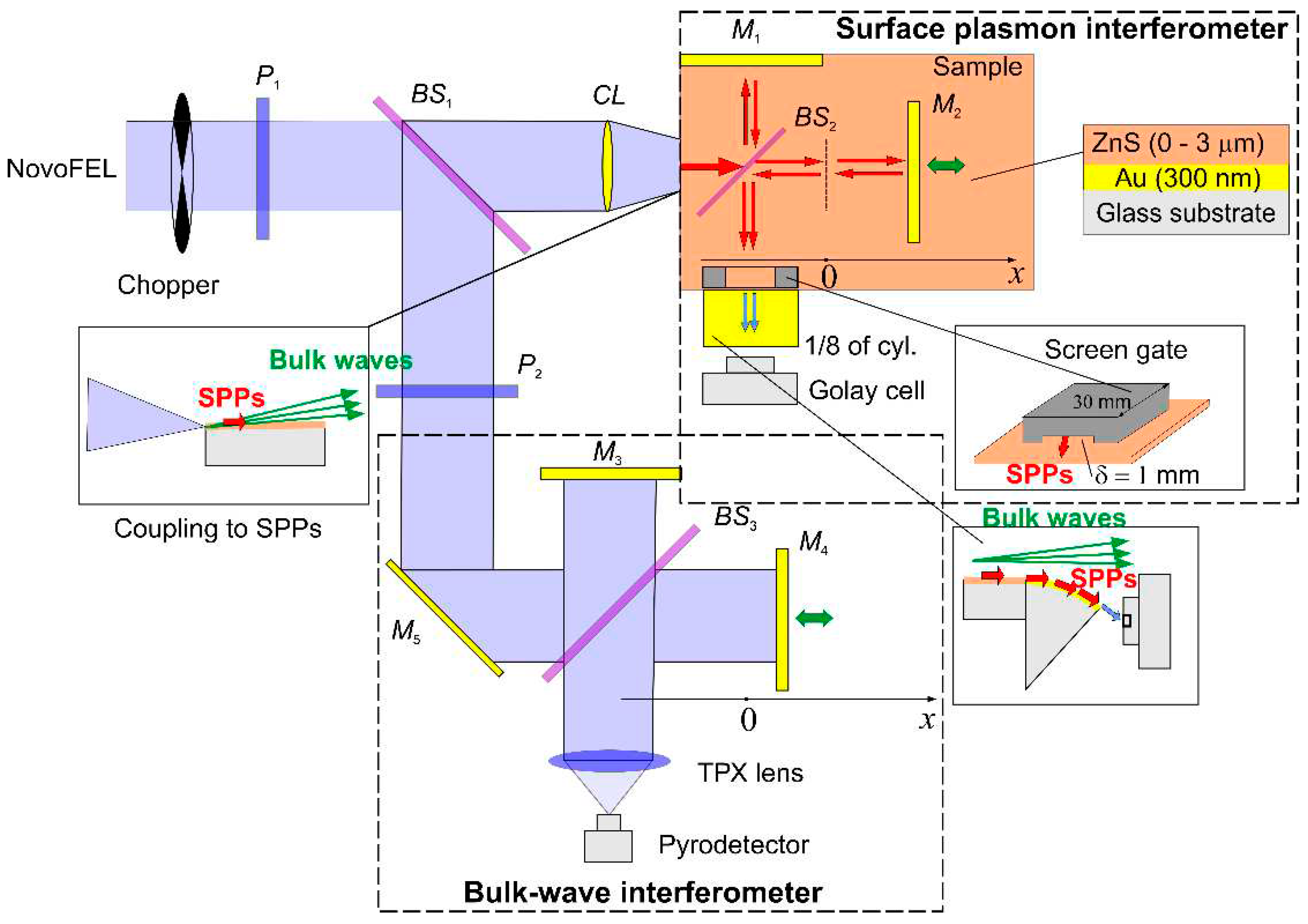
To measure the characteristics of THz surface plasmon polaritons (SPPs), we developed and created a plasmon Michelson interferometer, the schematic diagram of which is shown in [37,38], the results of first testing are presented in [39], detailed description of the SPP interferometer, its technical characteristics and measurement technique are presented in the paper [40]. The source of radiation was a unique installation of Budker Institute of Nuclear Physics SB RAS, the Novosibirsk free electron laser (NovoFEL) [41], which generates a periodic sequence of 100-ps pulses with frequency of 5.6 MHz. The NovoFEL radiation is linearly polarized and fully coherent in the beam cross section; the temporal coherence is 30 ÷100 ps (depending on the operating mode of the laser). The radiation wavelength was λ0 = 141 µm with line width of less than 1%. The average radiation power at the input to the interferometer was 30 ÷40 W, and the diameter of the Gaussian beam was 12 mm.
The use of the interferometer, similarly to the classical Michelson interferometer, relies on analysis of interferogram formed not by bulk waves, but by collinear SPP beams directed by the surface under study. The real part of the SPP refractive index ns was determined from comparison of the NovoFEL emission spectrum with the SPP spectrum resulting from the Fourier analysis of interferogram.
In the normal mode of NovoFEL operation, the emission spectrum is not stable enough: the wavelength shift can be of up to 0.2 μm during measurements. For the variations in the laser radiation spectrum to be taken into account, the interferogram formed by the NovoFEL radiation beams was recorded simultaneously with the plasmon interferogram. For this purpose, a Michelson interferometer for bulk waves (BWs) [39] was added to the scheme of the plasmon interferometer (Figure 1).
The p-component corresponding to the SPP polarization was extracted from the NovoFEL radiation beam entering the input of the installation (lithographic polarizer P1 was used). Polypropylene film beam splitter BS1 split the linearly polarized radiation into two beams. Cylindrical mirror CL focused the transmitted beam on the edge of the flat substrate of the plasmon interferometer, where, due to diffraction, the radiation was converted into SPPs. Mirror M5 directed the reflected beam, the intensity of which was controlled by polarizer P2, to the BW interferometer.
Figure 1. Optical circuit (top view) of THz SPP interferometer.
Preprints 77184 g001
In the plasmon interferometer, fixed (M1) and movable (M2) mirrors were used (40×20×5 mm3 glass plates with gold coating on the reflecting faces), and 40×25×1 mm3 plane-parallel plate BS2 of Zeonex polyimide, at an angle of 45° to the incident SPP beam, served as a SPP beam splitter [42]. The lower faces of the mirrors and the beam splitter were optically polished and closely adhered to the substrate, providing optical contact with its surface.
At the exit from the plasmon interferometer, combined collinear SPP beams from both arms passed to the convex surface of the cylindrical out-coupling element adjacent to the end of the substrate for conversion of SPPs into BWs. The element was a 1/8 of a cylinder with curvature radius of 60 mm; its convex polished surface contained a 300 nm layer of gold coated with a ZnS layer 1 μm thick. Having reached the opposite edge of the convex face of the element, the resulting SPP beam diffracted on it and was converted into BWs, registered by the radiation detector. The choice of such specific coupling element is due to the need for spatial separation of the BWs generated by the SPPs at the out-coupling edge of this element from the parasitic BWs arising at 1) conversion of the NovoFEL radiation into SPPs (accompanied by the formation of high-intensity diffracted BWs) [43], 2) the diffraction of the SPPs on the splitter and mirrors of the interferometer [44], and 3) the transition of the SPPs from the substrate to the out-coupling element. Moreover, an additional source of parasitic BWs was the scattering [45] of the SPPs on the roughness and optical inhomogeneities of the substrate surface, leading to the appearance of radiative losses of the SPPs [35]. An additional and effective screen from the parasitic BWs was a foam "gate" (35 mm long and 1 mm high) placed on the substrate at the point of its contact with the conversion out-coupling element.
The detection of the interfering BWs generated by the SPP beams on the free edge of the out-coupling element was done by an optoacoustic detector (Golay cell, TYDEX) of high sensitivity (NEP ≈ 1.4 10-10 W/Hz1/2 [46]). The need to use a highly sensitive receiver was due to the low signal intensity, large energy losses of the SPPs during their diffraction on the circuit elements, and SPP attenuation during propagation along the sample surface.
In the BW interferometer, the beams lost energy insignificantly (only in the reflection from splitter BS3). So, a less sensitive single-pixel pyroelectric receiver MG-33 (Novosibirsk Plant of Semiconductor Devices Vostok) was used to record BW interferograms [47,48]. The radiation directed to its 1×1 mm2 sensitive element was collected by a TPX lens with focal length of 50 mm.
Since the receivers applied can register only a time-varying radiation flux, a mechanical obturator was placed at the input of the setup, which modulated the radiation intensity with a frequency of 100 Hz. The signals from each receiver were recorded by two synchronous detectors SR-830 (Stanford Research), from the outputs of which the signals were sent to the two-channel digital oscilloscope (Handyscope 3), which operated in the recorder mode. The measured time dependences were digitized and written to a file.
Movable mirrors M2 and M4 were attached to the platforms of motorized stages (Standa), which shifted the mirrors along the x axis during scanning with a step of 2.5 μm. The scanning speed chosen was the highest possible (100 steps per second) at which the detectors had time to correctly register the recorded signals. The recording time for one pair of interferograms corresponding to a displacement of the movable mirrors by 30 mm was about 2 minutes.

2.2. Sample fabrication and testing

The samples were 100×150×11 mm3 flat glass plates, whose upper faces (100 ×150 mm2) were optically polished. By magnetron sputtering in an argon atmosphere at a pressure of 3·10-3 mbar with the use of the BOC Edwards Auto 500 device, an adhesive chromium sublayer (10 nm thick) was first deposited onto the polished face (heated to a temperature of 120°C), and then a layer of gold (grade 99.999%) 300 nm thick was applied. The layers were sputtered sequentially, from two different magnetrons, without time delays. A layer of zinc sulfide (ZnS) uniform in thickness (up to 3 µm) was deposited on the top of the gold by electron-beam evaporation (from a molybdenum crucible). The sequential deposition of the layers was done in one technological cycle, without removal of the substrate from the vacuum chamber. The thickness of the samples was measured on a “Spektr” ellipsometer developed by the Institute of Semiconductor Physics SB RAS.

2.3. Experimental data processing

Before the terahertz measurements, the optical circuits of both interferometers were adjusted with respect to the collimated beam of a diode laser (λ0 = 635 nm). The adjustment was done with high accuracy, since the difference in the refractive indices of SPPs on the samples, whose ZnS coatings differed in the thickness by 100 nm, was about 10-4. In addition, after placement of another sample (with a ZnS layer of a different thickness), it was necessary to re-adjust the SPP interferometer circuit, which took a lot of time because of high accuracy maintained. To reduce the adjustment time and take into account the slight misalignment between the interferometers, we carried out the measurements in two stages. First, two interferograms were measured simultaneously (on the plasmon and BW interferometers) in accordance with the scheme described in Section 2.1, when SPPs propagated along the sample surface. At the second stage of measurements, the NovoFEL radiation in the plasmon interferometer was not converted into SPPs, but was directed straight to beam splitter BS2 to result in an interferogram formed by the source radiation in the environment (air). Simultaneously with that, an interferogram was recorded on the BW interferometer. Thus, with the two stages of measurements, for each sample (differing in the thickness of the ZnS layer), two pairs of interferograms were obtained; moreover, for collection of statistics, the measurements were repeated four times with each of the samples.
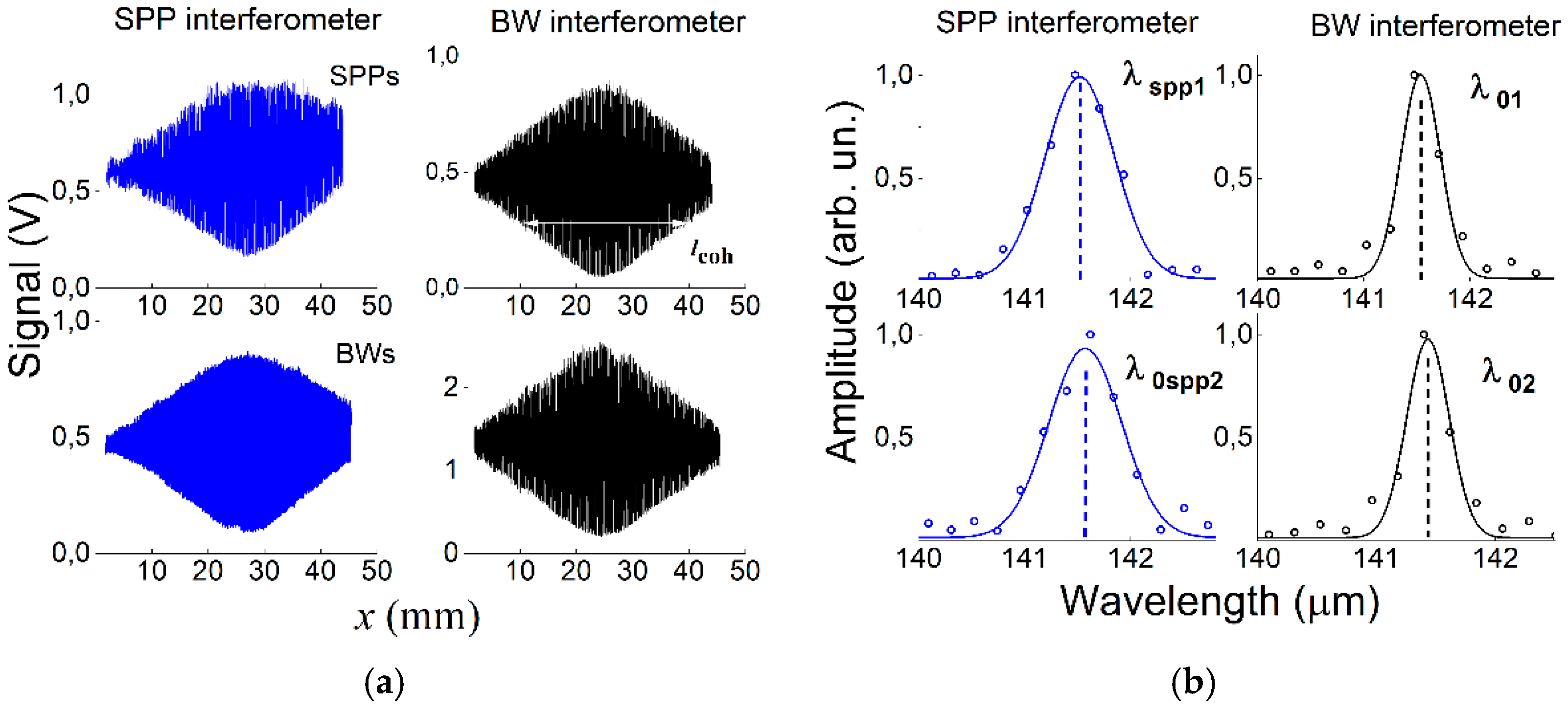
Figure 2a shows an example of SPP and BW interferograms. As the movable mirrors of the interferometers move along the x axis, the amplitudes of the sinusoids first increase, then reach the maximum, and decrease in the final section of the scanning. This is a typical symmetric form of the autocorrelation function for a coherent radiation source [49]. The amplitude envelope has a Gaussian profile, the width of which determines the length (duration) of coherence, which was 27 mm (90 ps) in this experiment. This is close to the maximum duration of the NovoFEL radiation pulse at operation in a stable mode (100 ps).
Figure 2. (a) Example of interferograms obtained with plasmon and bulk wave (BW) interferometers for “Au – ZnS layer 470 nm thick” sample. Left column: interferograms recorded with plasmon interferometer (upper graph, with SPP excitation; lower graph, without SPP excitation); right column: respective patterns obtained with BW interferometer. (b) Fourier spectra of SPPs and NovoFEL radiation generating SPPs; circles: reconstruction from interferograms in Figure 2a; lines: approximation of spectra with Gaussian function.
Preprints 77184 g002
By means of the Fourier transform, the SPP and NovoFEL radiation spectra were calculated from the interferograms (Figure 2b). The circles indicate the results of calculations of the components of the Fourier spectrum. The number of calculation points was determined by the length of the measured interferograms, which depends on the coherence length of the NovoFEL radiation (lcoh ≈ 27 mm). Next, the spectra were approximated with a Gaussian function of the form f ( x ) = A exp [ 1 2 ( x x c w ) 2 ] + f 0 and normalized to the value (А+f0). The w value defined the width of the spectrum. The value of the parameter xc, which describes the position of the central line of the spectrum, corresponded to the desired wavelength. The plots in Figure 3 show the wavelengths (central lines of the spectra): λspp1 and λ0spp2, found from interferograms obtained on the plasmon interferometer with and without SPP excitation, respectively; λ01 and λ02, the corresponding wavelengths of the NovoFEL radiation in air, determined with the BW interferometer.
Since the complex refractive index of the SPPs is defined as the ratio of the SPP wave number ks to the wave number of the radiation from the source in vacuum k0 = 2π/λ0,
n ˜ s = k s k 0 = n s + i κ s ,
the real part ns was found from the spectra shown in Figure 3 by the following formula:
n s = ( λ spp 1 / λ 0 spp 2 λ 01 / λ 02 ) Re ( n ˜ a ) ,
where the normalization to λ01/λ02 takes into account the shift in the NovoFEL generation spectrum that could occur during the time between recordings of interferograms with and without SPP excitation (see Section 2.1). The factor Re ( n ˜ a ) in expression (2) makes it possible to take into account the fact that the laser radiation propagates not in vacuum, but in air with the complex refractive index n ˜ a = 1 . 0002726 + i 0 . 0000039 [50,51]. For each sample, the average value of ns was found from four sets of interferograms.
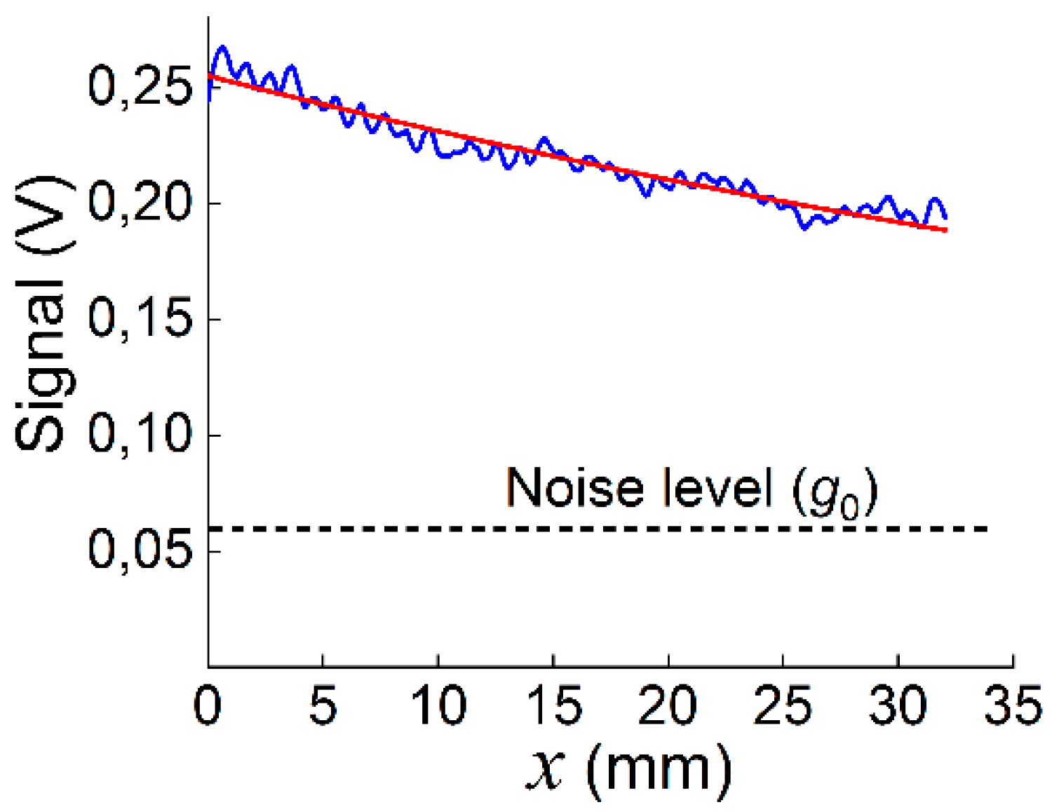
Figure 3. SPP intensity attenuation on “Au – ZnS layer 470 nm thick” sample at displacement of mirror М2 (see Figure 1) in plasmon interferometer, fixed mirror М1 closed by dump: blue line – experimental data, red line – approximation curve.
Preprints 77184 g003
To find the κs value we measured the attenuation of the SPP intensity at displacement of movable mirror M2 (see Figure 1) in the plasmon interferometer; in this case, fixed mirror M1 was covered by an absorbing plate. A typical dependence, measured on a sample with a ZnS layer 470 nm thick is shown in Figure 3. The figure also shows the result of approximation of the measurement results with a function of the form g ( x ) = B e x p ( 2 x / L s ) + g 0 , where Ls is the SPP propagation length. The exponent takes into account the 2х increase in the SPP path at displacement of the mirror by х. The noise level g0 was measured in the experiment and was set as an approximation parameter. For each sample, the average SPP propagation length Lav over four measurements was found and the κs value was calculated by the formula [11]
κ s = λ 0 4 π L av ,

3. Results

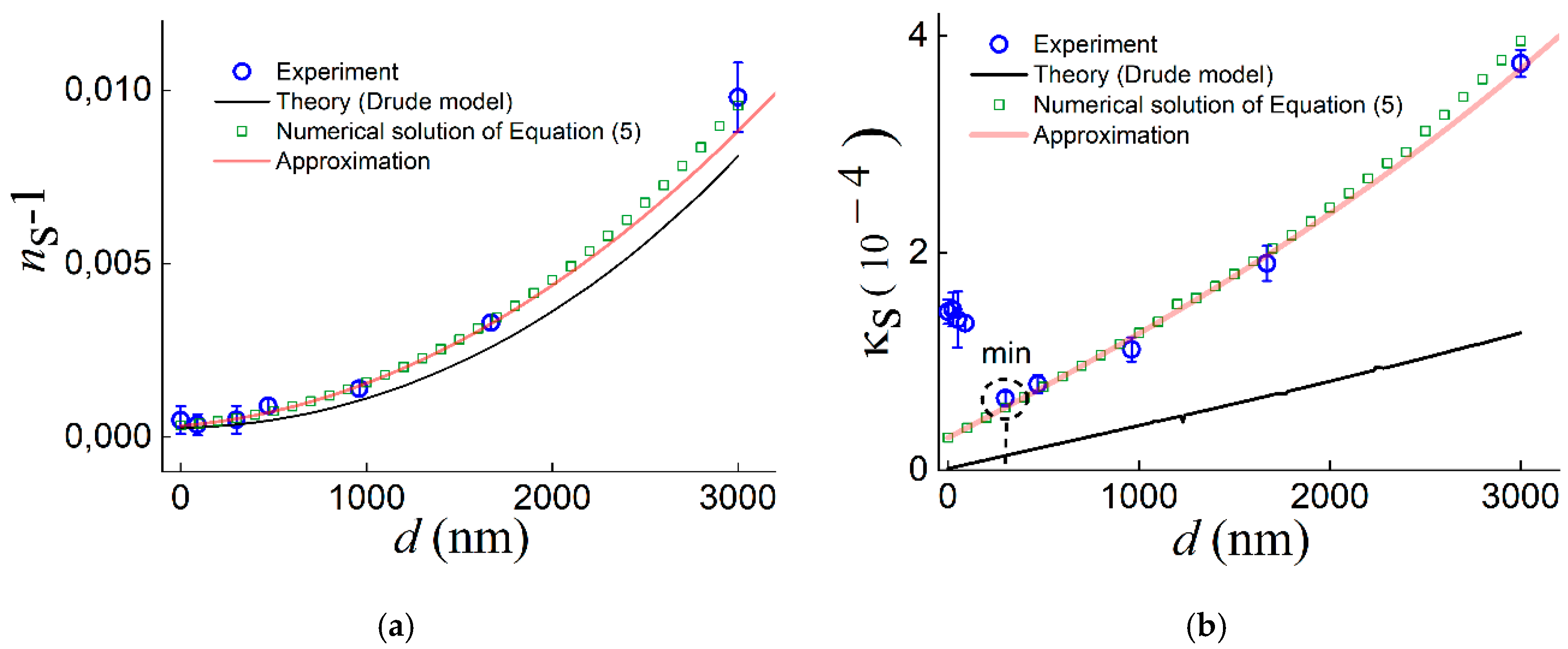
The experiments were carried out with a set of samples with flat substrates containing non-transparent layers of sputtered gold coated with a ZnS layer of thickness d =0 - 3000 nm. Figure 4a,b show the real part without unity ns-1 and the imaginary part κs of the SPP refractive index, respectively, found by the above methods, versus the d value. In these figures, the black lines show the calculated dependences obtained by numerical solution of the dispersion equation for the “gold - ZnS layer - air” structure at λ0 = 141 μm. In these calculations, the refractive index of ZnS was taken n d = 2 . 943 + i 0 . 01 [52], and the gold permittivity εm was calculated by the Drude model with the use of the reference values of plasma frequency ωp = 1.37·1016 s-1 and frequency of collisions of conduction electrons ωτ = 4.05·1013 s-1 [53]:
ε m ( ω ) = 1 ω p 2 ω 2 + ω τ 2 + i ω τ ω p 2 ω ( ω 2 + ω τ 2 ) ,
where ω = 2πс/λ0=1.34·1013 s-1 (c is the speed of light in vacuum).
From Figure 4a one can see that the value of ns-1 monotonically increases with d, all its experimental values lying above the calculated curve, which indicates that the real part Re(εm) of the dielectric constant of the deposited gold is less than the value predicted by the Drude model —according to the SPP theory, decrease in Re(εm) must be accompanied by increase in ns.
Figure 4. (a) Real part of SPP refractive index ns (without unity) and (b) imaginary part (SPP absorption index) κs vs. thickness d of ZnS layer on the gold surface: experiment (blue circles), approximation curves (red line), numerical solution of equation (5) for εm = -7000+i·3000 (green squares), and calculation by Drude model for εm = -104700+i·317180) (black line).
Preprints 77184 g004
Note that the determination errors for ns-1 for small thicknesses of ZnS (d ≤300 nm) and d = 3000 nm are noticeably larger than those for 300 nm < d < 3000 nm; the reason is the low intensity of the useful signal from the SPPs due to the low efficiency of SPP generation in the plasmon interferometer at such thicknesses of the dielectric layer.
The value of the SPP refractive index on uncoated gold was ns≈ 1.0005, which corresponds to the SPP phase velocity ϑph = c/ns ≈ 0.9995 c. Similar values of SPP phase velocities were also obtained for thick aluminum wire in experiments performed on a TDS spectrometer [54], where ϑph was determined from the time delay of a THz SPP pulse relative to a light pulse propagating in air.
As for the imaginary part κs of the SPP refractive index, which characterizes the SPP decay, at increase in the thickness d of the cover layer, the measured values (blue circles in Figure 4b) first decrease, reach the minimum at d ≈ 300 nm, and then grow monotonically. This behavior of κs was explained in [35] and is associated with the decrease in the radiative losses of SPPs at deposition of a dielectric layer onto the metal surface. At some d = d0 (300 nm in our case), the integral losses of SPPs reach the minimum, and at d > d0, their growth is due to the predominance of the Joule losses over the radiative losses because of the monotonic increase of the fraction of SPP field energy transferred into the metal with d growth.

3.1. Determination of the permittivity of metal surface from the SPP characteristics on a set of samples with a dielectric layer of various thicknesses

In this section, we consider an approximation method for finding the metal permittivity, which uses the n ˜ s values found for a set of samples with ZnS coatings of various thicknesses.
To determine the effective permittivity εm of a metal surface guiding the SPPs and containing a thin-layer coating of thickness d with permittivity εd from the found complex refractive index n ˜ s of the SPPs, it is necessary to solve (with respect to εm) the SPP dispersion equation for the three-layer structure “metal – dielectric layer – environment” [55]:
tanh ( k 0 d n ˜ s 2 ε d ) = n ˜ s 2 ε d × ( n ˜ s 2 ε a ε a + n ˜ s 2 ε m ε m ) ε d ( n ˜ s 2 ε a n ˜ s 2 ε m ε a ε m + n ˜ s 2 ε d ε d 2 ) ,
where εa is the permittivity of the environment.
Transcendental equation (5) can be solved numerically, but the solution is very sensitive to small variations in n ˜ s within the measurement error, which can result in a large error in determination of the metal permittivity εm. Therefore, we have developed an εm determination method based on the approximation of the (ns-1)(d) and κs(d) dependences measured for a series of samples with different ZnS coating thicknesses.
Since in the THz range εm >> εd, εa, the k 0 d < < 1 / ε m condition is met at d<<λ. Expanding both parts of equation (5) into a Taylor series with respect to a small correction to the refractive index n ˜ s because of the dielectric coating on the metal, we obtain an approximate formula for calculating the surface impedance of the three-layer structure (see Appendix A):
ξ i × ( ε d ε m 2 ε a + ε m × ( ε a + ε m ) + k 0 d ε m × [ ε a ( ε m ε d ) ε m ε d ] ) ε d ( ε a + ε m ) × ( k 0 d ε d ε m 2 ε a + ε m + ε m ) ,
where
n ˜ s = ε a ( ε a ξ ) 2 .
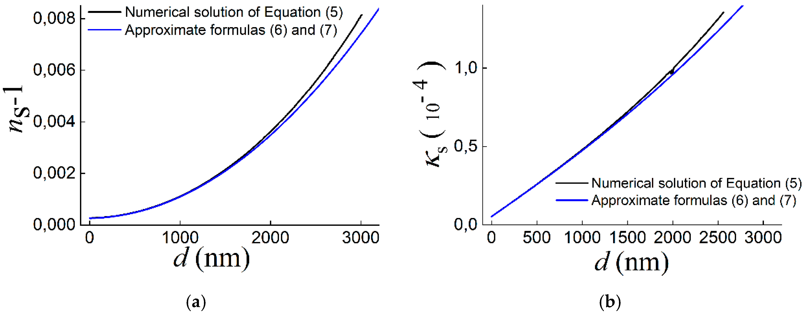
The dependences of ns -1 and κs on the ZnS layer thickness d were found by formulas (6) and (7) for the gold permittivity εm calculated according to the Drude model (blue lines in Figure 5). In the figure, the red lines show the results of the numerical solution of Eq. (5). It can be seen that at d ≤ 1500 nm, the approximate and exact solutions practically coincide, and at 1500 nm < d ≤ 3000 nm they differ by no more than 8%.
Figure 5. Real part (without unity) ns and imaginary part κs of SPP refractive index in structure “gold – ZnS layer of thickness d – air” vs. d calculated by approximate formulas (6) and (7) (black lines) and by numerical solution of dispersion equation (5) (blew lines). Calculations used gold permittivity εm = -104700+i·317180, calculated by Drude model at λ0 =141 μm.
Preprints 77184 g005
Then the experimental dependences (ns -1)(d ) and κs(d) were approximated by means of a Matlab program, using the least squares method to find the minimum deviations of the experimental values from the corresponding functions Re ( n ˜ s 1 ) and Im ( n ˜ s ) ( n ˜ s was found by formula (7)). The real and imaginary parts of the gold permittivity εm were varied as parameters. The search for the solution for both functions was performed in the range of ZnS layer thicknesses 300 nm ≤ d ≤ 1670 nm. The domain of the functions did not include small thicknesses (d < 300 nm), when the SPP decay is governed by the radiative losses, not taken into account by Eq. (5); at d = 3000 nm, the approximate formula gives noticeable deviations from the exact solution.
As a result of the approximation, the permeability of the deposited gold was found: the real part was Re(εm) ≈ -7000±3000, and the imaginary was Im(εm) ≈ 3000±1300. The approximation dependences (ns-1)(d) and κs(d) are shown by the gray lines in Figure 4. The large errors (of up to 40%) in the determination of εm by this method are due to the closeness of the refractive index ns of the THz SPPs to the refractive index of air, which necessitates a higher accuracy in finding the ns value.
In Figure 4, the green squares show the results for the numerical solution of dispersion equation (5) by the downhill method [56] at εm = -7000+ i·3000. It can be seen that the results of the calculation at d ≤ 1700 nm almost coincide with the curves obtained by approximate formula (7), which indicates the possibility of its effective application for evaluation calculations of the complex refractive index of THz SPPs in a three-layer structure in the presence of a dielectric coating layer of subwavelength thickness on the metal.
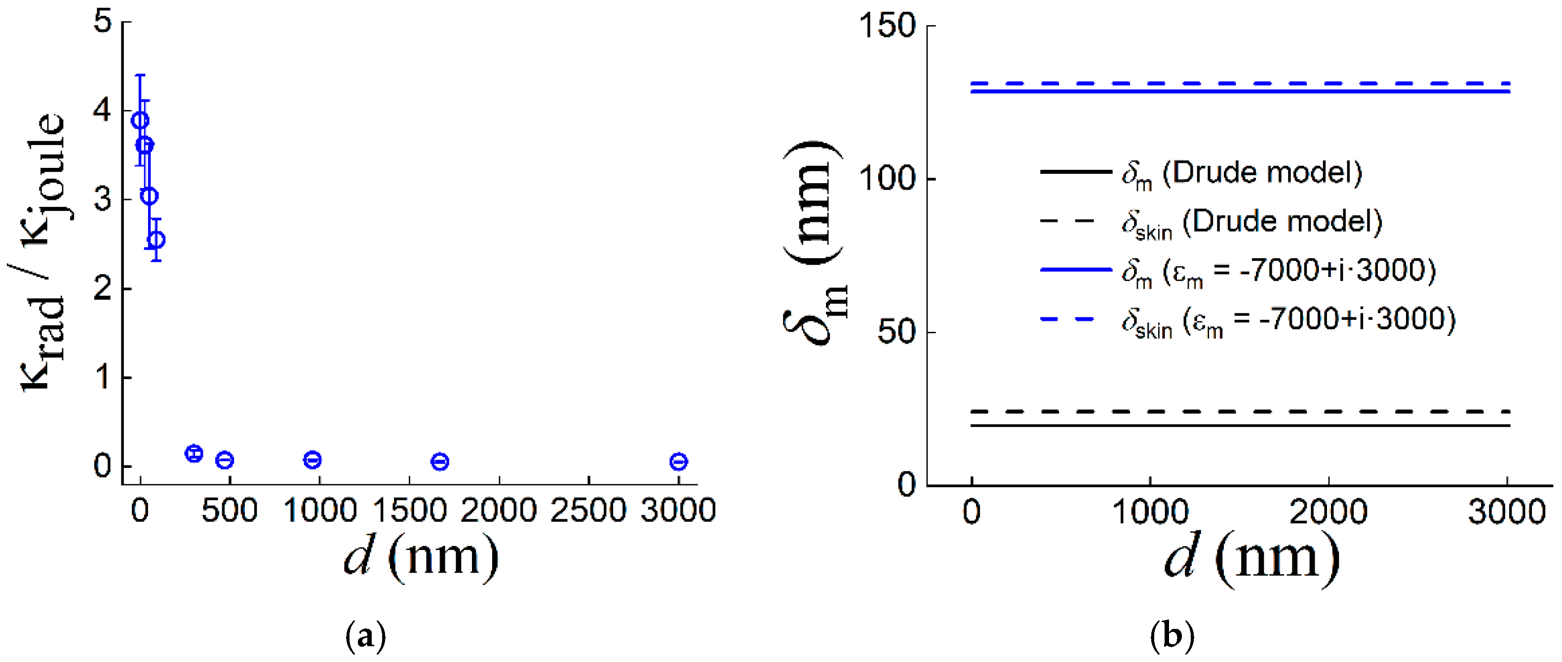
It was already noted above that the presence of a dielectric layer on the metal surface leads to increase in the fraction of SPP field energy transferred into the metal. In this case, the depth δm of the penetration of the SPP field into the metal is practically independent of the coating thickness, as evidenced by the graphs in Figure 6b, obtained from solution of equation (5) for the "gold - ZnS layer of thickness d - air" structure. It can be seen that with the gold permeability found by the approximation method from the experimental results, the δm value is approximately six times greater than that for the permeability calculated by the Drude model. Therefore, for the deposited gold layer to be non-transparent for the THz SPP field (which excludes the effect of the substrate on the SPP characteristics), its thickness must be 150–200 nm at least.
From the plot of κs(d) in Figure 6a, it can be seen that at small thicknesses d < 300 nm, the loss of SPPs in the experiment is much greater than the calculations predict. This is explained by the presence of radiative losses of SPPs, which are not taken into account either by the approximate formulas or by the dispersion equation; starting from d ≈ 300 nm (where the minimum of the integral losses of SPPs is reached, and their radiative losses become relatively small compared with the Joule losses), the measured values of the absorption coefficient of SPPs approach the calculated dependence.
Figure 6. (a) Ratio of radiative and Joule losses of SPPs, calculated by formula (8) at λ0 = 141 μm vs. thickness d of the ZnS layer in “deposited gold – ZnS layer – air” structure; (b) penetration depth δm (in terms of intensity) of SPP field into metal for "gold - ZnS layer with thickness d - air" structure at λ0 = 141 µm and gold permeability εm calculated according to Drude model (black line) and εm = -7000+i·3000, determined by approximation method from characteristics of SPPs (blew line). Dotted lines: corresponding values of skin layer thickness.
Preprints 77184 g006
Based on this interpretation of the existence of minimum of the losses κs(d) and the assumption that other mechanisms of losses contribute negligibly to the total SPP decay, the SPP radiative losses can be estimated by the following formula:
κ rad = κ s κ Joule ,
where κs is the total SPP losses measured in the experiment; κJoule is the Joule SPP losses determined from the solution of equation (5).
Figure 6a shows the ratio of radiative losses estimated by formula (8) to Joule losses at different thicknesses d of the ZnS layer, calculated from the solution of equation (5) with substitution of εm = -7000+i·3000 (found by the approximation method) into it. In this case, in the absence of a dielectric layer on the metal surface, the radiative losses exceed the Joule losses about four-fold. However, as d grows, this ratio decreases monotonically to zero at d ≥ 960 nm, when the SPP decay is determined mainly by losses in the metal.

3.2. Determination of the effective dielectric constant of metal surface from SPP characteristics on one sample

In Section 3.1, we described an estimation of the dielectric permittivity of metal εm via application of the approximation method to the measurements of the characteristics of THz SPPs on a set of samples with different thicknesses of dielectric layers on the metal surface. Despite its rather high reliability, this method is very laborious for a rapid assessment of the dielectric constant of metal (metallized) optical surfaces. Therefore, it is desirable (in view of practical applications) to have a method for determination of εm from the complex refractive index n ˜ s = n s + i κ s of THz SPPs, found from measurements of its real and imaginary parts on only one sample.
From equation (5), we obtained an approximate formula for calculating εm from the measured characteristics of SPPs (see Appendix A):
ε m ε d 2 [ k 0 d ( ε a ε d ) + i ε d ξ ] 2 ,
where the surface impedance ξ is found from formula (6).
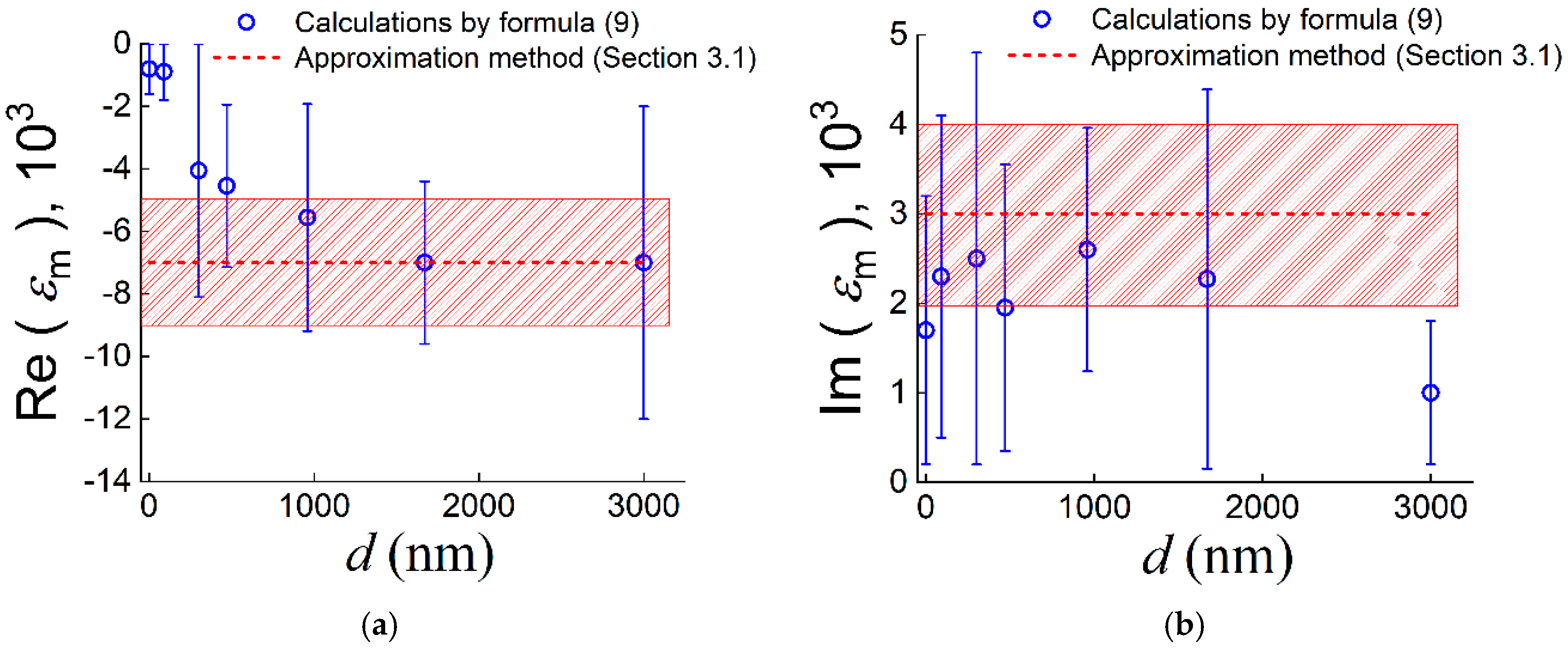
As was established above, radiative losses make a predominant contribution to the SPP decay on a metal without a dielectric coating layer, which leads to large errors in the determination of εm. Therefore, it is necessary to find a layer thickness d range in which the error in determination of εm is not so large. For this purpose, the permittivity εm of deposited gold was calculated by formula (9) with substitution of experimentally determined values of n ˜ s for samples with different thicknesses d of the ZnS layer into it.
The found values of the real Re(εm) and imaginary Im (εm) parts of the gold permittivity are shown by black circles in Figure 7. The errors on the graphs correspond to the maximum permittivity deviations calculated in the ranges of experimental values ns±Δns and κs±Δκs, where Δns and Δκs are the corresponding measurement errors. It can be seen that the values of Re(εm) and Im(εm) at small thicknesses of the ZnS layer ( d < 300 nm) differ greatly from the approximation values, and at d  300 nm, they approach the approximation values asymptotically (except for Im(εm) at d = 3000 nm, where already formula (9) gives insufficiently reliable results). This character of the dependence εm(d) can be explained by the fact that formula (9) does not take into account the radiative losses of SPPs; at larger thicknesses of the dielectric layer, when the radiative losses becomes much less than the thermal losses, formula (9) describes the experiment much better.
Figure 7. (a) Real and (b) imaginary parts of gold permittivity εm vs. thickness d of ZnS layer (blew circles), calculated by formula (9) with n ˜ s ( d ) values found from results of measurements presented in Figure 4. Red dotted lines: values of both parts of gold permeability, found by approximation method; rectangular areas filled with oblique red lines: corresponding standard deviation ranges.
Preprints 77184 g007
Note that according to the performed calculations, the real part Re(εm) of the permittivity of gold without a ZnS coating layer (d = 0) turned out to be equal to – 800 (see Figure 7). This value of Re(εm)) is in agreement with the estimates given in earlier publications on THz SPP refractometry of deposited gold without a dielectric coating layer, implemented on a TDS spectrometer [31] and with FEL radiation [24]. However, as follows from the above, this value of Re(εm) differs from its real value of -7000 almost 10 times. In our opinion, the erroneous estimation of Re(εm) in previous works on THz SPP refractometry was because of the unaccounted significant radiative losses of SPPs on a metal surface free without a coating layer.
It is important to note that the obtained errors for metal effective permittivity (see Figure 7) are very large (reach 50%). It is clear that its more reliable determination by the proposed method of SPP refractometry requires higher accuracy of finding the real part of the SPP refractive index from the recorded interferograms. For the accuracy of determination of the metal permittivity to be 20% (for thicknesses d ≥ 500 nm), it is necessary to determine ns with an error not worse than 10-4 (with an actual error of 10% for κs, which depends on the signal-to-noise ratio, adjustment, and stability of the intensity of NovoFEL radiation. For such accuracy for ns, the stability of the radiation source in terms of wavelength during recording of interferogram must be not worse than 0.01 µm (for λ0 = 141 µm), while the width of the generation line must be an order of magnitude smaller than 1.0 ÷1.5 µm in the normal operation mode. This can be achieved via reduction of the measurement time with faster and more sensitive detectors, as well as sources of coherent THz radiation that are more stable than FELs, such as gas lasers [57], backward wave oscillators [58], gyrotrons [59], and quantum-cascade lasers [60].
Note that it is possible to increase the stability of NovoFEL radiation to temporal variations in the radiation wavelength at operation in the mode of negative detuning of the electron bunch repetition rate from the repetition rate of light pulses inside the FEL optical resonator, accompanied by a decrease in the average radiation power [61]. In operation in this mode, a stable single-mode generation regime was established, the linewidth of which reached the maximum possible narrow value (0.25%) [49], while the wavelength shift in 15 minutes was not more than 0.1 of the width of the generated radiation spectrum (0.04 μm at λ0 =141 µm), which is close to the desired accuracy. However, to achieve such a generation mode, a long and laborious adjustment of the NovoFEL parameters is necessary.
4. Conclusions

The studies performed have shown that for correct determination of the effective permittivity εm of a metal surface by the proposed method of terahertz (THz) plasmon interferometric refractometry or by other methods based on analysis of the characteristics of surface plasmon polaritons (SPPs), the measurements must be performed in presence of a dielectric layer on the metal. The thickness of the dielectric coating should be large enough for the radiative losses because of SPP scattering on the surface roughness and inhomogeneities to be significantly less than the Joule losses of SPPs in the metal, but not large enough to make it impossible to measure the SPP decay with an acceptable accuracy. The choice of the optimal thickness of the dielectric layer depends on many factors [62]: the type of the metal, its state (surface of bulk or deposited metal), substrate roughness, optical homogeneity of the metal film, and the optical density of the dielectric. The proposed method of plasmon refractometry of a conducting surface can be applied not only to metals, but also to other materials used in THz plasmonics (doped semiconductors [31], graphene [63], dielectrics on absorption lines, etc.), which provide a macroscopic propagation length of the surface wave. Using the εm value found by the method proposed will enable more adequate modeling of the operation of elements and devices of THz plasmonics, plasmonic sensors, and communication lines.

Author Contributions

Conceptualization, A.K.N. and V.V.G.; methodology, V.V.G. and A.K.N.; software, V.V.G., A.K.N., I.A.K.; formal analysis, V.V.G. and A.K.N.; investigation, V.V.G.; resources, A.G.L and I.A.A.; data curation, V.V.G.; writing—original draft preparation, V.V.G. and A.K.N.; writing—review and editing, V.V.G. and A.K.N.; visualization, V.V.G.; supervision, V.V.G. and A.K.N.; project administration, V.V.G.; funding acquisition, V.V.G. and A.K.N. All authors have read and agreed to the published version of the manuscript.

Funding

The work was done on the equipment of the shared research center SSTRC on the basis of the Novosibirsk FEL at BINP SB RAS.

Institutional Review Board Statement

Not applicable.

Informed Consent Statement

Not applicable.

Data Availability Statement

The data presented in this study are available upon reasonable request from the corresponding authors.

Acknowledgments

Authors thanks to Novosibirsk free electron laser team for assistants in the experiments. The authors acknowledge core facilities “VTAN” (Novosibirsk State University) for the access to its experimental equipment.

Conflicts of Interest

The authors declare no conflict of interest.

Appendix A

On the metal-air interface, the tangential component Eτ of the electric field vector is in the following relation to the magnetic field vector B:
Eτ = ξ·[nxB],
where the unit vector n is directed along the outer normal to the metal surface, and the parameter
ξ = ζ i ε a k 0
is referred to as the surface impedance ( ζ = k 0 n ˜ 2 s ε a is the rate of decay of the SPP field in air, and εa is the dielectric constant of air).
In the presence on the metal surface of a dielectric layer with εd and thickness d < < 1 / k 0 ε m , the impedance of the “metal – dielectric layer – air” structure can be calculated by the following approximate formula [64]:
ξ = 1 ε m i ( ε d ε a ε d ) k 0 d .
As can be seen from (12), for sufficiently thick layers ( k 0 d > 1 / ε m ), the correction to the impedance due to the dielectric layer is significant, and formula (12) becomes inapplicable.
When d = 0, dispersion equation (5) for a three-layer structure has the root n ˜ 0 s = ε a ε m / ( ε a + ε m ) . Substituting n ˜ s 2 = ( n ˜ 0 s ) 2 + d x into (5) and expanding both sides of this equation into the Taylor series to terms linear in d, we obtain a linear (with respect to x) equation, and if εm >> εd, εa, we come up to formula (12). This expansion is valid if the correction d·x is small compared with ( n ˜ 0 s ) 2 ε a , ( n ˜ 0 s ) 2 ε d , ( n ˜ 0 s ) 2 ε m , the first condition
d x < < ( n ˜ 0 s ) 2 ε a = ε a 2 ε a + ε m .
being the most difficult to satisfy. Because
ξ = n ˜ 2 s ε a i ε a = ε a 2 ε a + ε m + d x / ( i ε a )
condition (13) means that the second term in (12) is small compared with the first one, i.e., k 0 d < < 1 / ε m . If, on the contrary, k 0 d > 1 / ε m , then we must take into account the fact that the correction to n ˜ 2 s , which depends on k0·d, significantly changes the terms that contain n ˜ 2 s ε a .
On the other hand, the terms in (5) that contain n ˜ 2 s ε d and n ˜ 2 s ε m are much less sensitive to the correction k0·d. Therefore, the zero approximation n ˜ 2 s = n ˜ 2 0 can be substituted into these terms. As a result, we obtain a simple equation for ξ. Replacing the hyperbolic tangent on the left side of equation (5) with its argument (since the argument is very small), we obtain an approximate expression for the surface impedance of the three-layer medium (see formula (6)).
Approximate formula (7) for metal permittivity εm was obtained from (6) with the help of the analytical solver in the Wolfram Mathematica package.

References

  1. Ordal, M.A.; Long, L.L.; Bell, R.J.; Bell, S.E.; Bell, R.R.; Alexander, R.W.; Ward, C.A. Optical Properties of the Metals Al, Co, Cu, Au, Fe, Pb, Ni, Pd, Pt, Ag, Ti, and W in the Infrared and Far Infrared. Appl. Opt. 1983, 22, 1099. [Google Scholar] [CrossRef] [PubMed]
  2. Pandey, S.; Gupta, B.; Chanana, A.; Nahata, A. Non-Drude like Behaviour of Metals in the Terahertz Spectral Range. Advances in Physics: X 2016, 1, 176–193. [Google Scholar] [CrossRef]
  3. Parshin, V.V.; Myasnikova, S.E. Metals Reflectivity at Frequencies 100-360 GHz. In Proceedings of the 2005 Joint 30th International Conference on Infrared and Millimeter Waves and 13th International Conference on Terahertz Electronics; IEEE: Williamsburg, VA, USA, 2005; Vol. 2, pp. 569–570. [Google Scholar]
  4. Naftaly, M.; Dudley, R. Terahertz Reflectivities of Metal-Coated Mirrors. Appl. Opt. 2011, 50, 3201. [Google Scholar] [CrossRef]
  5. Johnson, P.B.; Christy, R.W. Optical Constants of the Noble Metals. Phys. Rev. B 1972, 6, 4370–4379. [Google Scholar] [CrossRef]
  6. Gatesman, A.J.; Giles, R.H.; Waldman, J. High-Precision Reflectometer for Submillimeter Wavelengths. J. Opt. Soc. Am. B 1995, 12, 212. [Google Scholar] [CrossRef]
  7. Handbook of optical constants of solids (V.1). / Ed by E.D. Palik. Academic Press, 2016. 824 P.
  8. Reuter, G.E.H.; Sondheimer, E.H. Theory of the Anomalous Skin Effect in Metals. Nature 1948, 161, 394–395. [Google Scholar] [CrossRef]
  9. Ordal, M.A.; Bell, R.J.; Alexander, R.W.; Long, L.L.; Querry, M.R. Optical Properties of Au, Ni, and Pb at Submillimeter Wavelengths. Appl. Opt. 1987, 26, 744. [Google Scholar] [CrossRef]
  10. Brändli, G.; Sievers, A.J. Absolute Measurement of the Far-Infrared Surface Resistance of Pb. Phys. Rev. B 1972, 5, 3550–3557. [Google Scholar] [CrossRef]
  11. Surface Polaritons: Electromagnetic Waves at Surfaces and Interfaces; Agranovich, V.M.; Mills, D.L. (Eds.) Modern problems in condensed matter sciences; North-Holland Pub. Co. : Sole distributors for the USA and Canada, Elsevier Science Pub. Co: Amsterdam; New York, 1982; ISBN 978-0-444-86165-8. [Google Scholar]
  12. Maier, S.A. Plasmonics: The Promise of Highly Integrated Optical Devices. IEEE J. Select. Topics Quantum Electron. 2006, 12, 1671–1677. [Google Scholar] [CrossRef]
  13. Zhu, W.; Agrawal, A.; Nahata, A. Planar Plasmonic Terahertz Guided-Wave Devices. Opt. Express 2008, 16, 6216. [Google Scholar] [CrossRef]
  14. Zhang, X.; Xu, Q.; Xia, L.; Li, Y.; Gu, J.; Tian, Z.; Ouyang, C.; Han, J.; Zhang, W. Terahertz Surface Plasmonic Waves: A Review. Adv. Photon. 2020, 2, 1. [Google Scholar] [CrossRef]
  15. Pendry, J.B.; Martín-Moreno, L.; Garcia-Vidal, F.J. Mimicking Surface Plasmons with Structured Surfaces. Science 2004, 305, 847–848. [Google Scholar] [CrossRef] [PubMed]
  16. Maier, S.A.; Andrews, S.R. Terahertz Pulse Propagation Using Plasmon-Polariton-like Surface Modes on Structured Conductive Surfaces. Appl. Phys. Lett. 2006, 88, 251120. [Google Scholar] [CrossRef]
  17. Williams, C.R.; Andrews, S.R.; Maier, S.A.; Fernández-Domínguez, A.I.; Martín-Moreno, L.; García-Vidal, F.J. Highly Confined Guiding of Terahertz Surface Plasmon Polaritons on Structured Metal Surfaces. Nature Photon 2008, 2, 175–179. [Google Scholar] [CrossRef]
  18. Kretschmann, E. Die Bestimmung optischer Konstanten von Metallen durch Anregung von Oberflächenplasmaschwingungen. Z. Physik 1971, 241, 313–324. [Google Scholar] [CrossRef]
  19. Kitajima, H.; Hieda, K.; Suematsu, Y. Use of a Total Absorption ATR Method to Measure Complex Refractive Indices of Metal-Foils. J. Opt. Soc. Am. 1980, 70, 1507. [Google Scholar] [CrossRef]
  20. Regalado, L.E.; Machorro, R.; Siqueiros, J.M. Attenuated-Total-Reflection Technique for the Determination of Optical Constants. Appl. Opt. 1991, 30, 3176. [Google Scholar] [CrossRef]
  21. Owner-Petersen, M.; Zhu, B.-S.; Dalsgaard, E. Extreme Attenuation of Total Internal Reflection Used for Determination of Optical Properties of Metals. J. Opt. Soc. Am. A 1987, 4, 1741. [Google Scholar] [CrossRef]
  22. Lafait, J.; Abeles, F.; Theye, M.L.; Vuye, G. Determination of the Infrared Optical Constants of Highly Reflecting Materials by Means of Surface Plasmon Excitation-Application to Pd. J. Phys. F: Met. Phys. 1978, 8, 1597–1606. [Google Scholar] [CrossRef]
  23. Zhizhin, G.N.; Morozov, N.N.; Moskalova, M.A.; Sigarov, A.A.; Shomina, E.V.; Yakovlev, V.A.; Grigos, V.I. Surface Electromagnetic Wave Absorption on Copper Surfaces with Langmuir Films Using Co2 Laser Excitation. Thin Solid Films 1980, 70, 163–168. [Google Scholar] [CrossRef]
  24. Gerasimov, V.V.; Knyazev, B.A.; Nikitin, A.K.; Zhizhin, G.N. A Way to Determine the Permittivity of Metallized Surfaces at Terahertz Frequencies. Appl. Phys. Lett. 2011, 98, 171912. [Google Scholar] [CrossRef]
  25. Auston, D.H.; Cheung, K.P. Coherent Time-Domain Far-Infrared Spectroscopy. J. Opt. Soc. Am. B 1985, 2, 606. [Google Scholar] [CrossRef]
  26. Grischkowsky, D.; Keiding, S.; Van Exter, M.; Fattinger, Ch. FarInfrared Time-Domain Spectroscopy with Terahertz Beams of Dielectrics and Semiconductors. J. Opt. Soc. Am. B 1990, 7, 2006. [Google Scholar] [CrossRef]
  27. Zhou, D.; Parrott, E.P.J.; Paul, D.J.; Zeitler, J.A. Determination of Complex Refractive Index of Thin Metal Films from Terahertz Time-Domain Spectroscopy. Journal of Applied Physics 2008, 104, 053110. [Google Scholar] [CrossRef]
  28. Yasuda, H.; Hosako, I. Measurement of Terahertz Refractive Index of Metal with Terahertz Time-Domain Spectroscopy. Jpn. J. Appl. Phys. 2008, 47, 1632–1634. [Google Scholar] [CrossRef]
  29. Han, P.Y.; Tani, M.; Usami, M.; Kono, S.; Kersting, R.; Zhang, X.-C. A Direct Comparison between Terahertz Time-Domain Spectroscopy and Far-Infrared Fourier Transform Spectroscopy. Journal of Applied Physics 2001, 89, 2357–2359. [Google Scholar] [CrossRef]
  30. Isaac, T.H.; Barnes, W.L.; Hendry, E. Determining the Terahertz Optical Properties of Subwavelength Films Using Semiconductor Surface Plasmons. Appl. Phys. Lett. 2008, 93, 241115. [Google Scholar] [CrossRef]
  31. Pandey, S.; Liu, S.; Gupta, B.; Nahata, A. Self-Referenced Measurements of the Dielectric Properties of Metals Using Terahertz Time-Domain Spectroscopy via the Excitation of Surface Plasmon-Polaritons. Photon. Res. 2013, 1, 148. [Google Scholar] [CrossRef]
  32. Nazarov, M.M.; Shkurinov, A.P.; Garet, F.; Coutaz, J.-L. Characterization of Highly Doped Si Through the Excitation of THz Surface Plasmons. IEEE Trans. THz Sci. Technol. 2015, 5, 680–686. [Google Scholar] [CrossRef]
  33. Kapitulnik, A.; Deutscher, G. Percolation Scale Effects in Metal-Insulator Thin Films. J Stat Phys 1984, 36, 815–826. [Google Scholar] [CrossRef]
  34. Tomilina, O.A.; Berzhansky, V.N.; Tomilin, S.V. The Influence of the Percolation Transition on the Electric Conductive and Optical Properties of Ultrathin Metallic Films. Phys. Solid State 2020, 62, 700–707. [Google Scholar] [CrossRef]
  35. Gerasimov, V.V.; Knyazev, B.A.; Lemzyakov, A.G.; Nikitin, A.K.; Zhizhin, G.N. Growth of Terahertz Surface Plasmon Propagation Length Due to Thin-Layer Dielectric Coating. J. Opt. Soc. Am. B 2016, 33, 2196. [Google Scholar] [CrossRef]
  36. Kumar, M.; Porsezian, K. A Comparative Study of Surface Plasmon Polariton Propagation Characteristics of Various Metals.; Uttar Pradesh, India, 2016; p. 080080.
  37. Nikitin, A.K.; Khitrov, O.V.; Gerasimov, V.V.; Khasanov, I.S.; Ryzhova, T.A. In-Plane Interferometry of Terahertz Surface Plasmon Polaritons. J. Phys.: Conf. Ser. 2019, 1421, 012013. [Google Scholar] [CrossRef]
  38. Nikitin, A.K.; Khitrov, O.V.; Gerasimov, V.V. Quality Control of Solid Surfaces by the Method of Surface Plasmon Interferometry in the Terahertz Range. J. Phys.: Conf. Ser. 2020, 1636, 012037. [Google Scholar] [CrossRef]
  39. Gerasimov, V.V.; Nikitin, A.K.; Khitrov, O.V.; Lemzyakov, A.G. Experimental Demonstration of Surface Plasmon Michelson Interferometer at the Novosibirsk Terahertz Free-Electron Laser. In Proceedings of the 2021 46th International Conference on Infrared, Millimeter and Terahertz Waves (IRMMW-THz); IEEE: Chengdu, China, August 29 2021; pp. 1–2. [Google Scholar] [CrossRef]
  40. Gerasimov, V. V.; Nikitin A., K.; Lemzyakov, A. G. Planar Michelson interferometer using terahertz surface plasmons. Instruments and Experimental Techniques 2023, 66, 423–434. [Google Scholar] [CrossRef]
  41. Shevchenko, O.A.; Vinokurov, N.A.; Arbuzov, V.S.; Chernov, K.N.; Davidyuk, I.V.; Deichuly, O.I.; Dementyev, E.N.; Dovzhenko, B.A.; Getmanov, Ya.V.; Gorbachev, Ya.I.; et al. The Novosibirsk Free-Electron Laser Facility. Bull. Russ. Acad. Sci. Phys. 2019, 83, 228–231. [Google Scholar] [CrossRef]
  42. Islam, M.S.; Cordeiro, C.M.B.; Nine, M.J.; Sultana, J.; Cruz, A.L.S.; Dinovitser, A.; Ng, B.W.-H.; Ebendorff-Heidepriem, H.; Losic, D.; Abbott, D. Experimental Study on Glass and Polymers: Determining the Optimal Material for Potential Use in Terahertz Technology. IEEE Access 2020, 8, 97204–97214. [Google Scholar] [CrossRef]
  43. Gerasimov, V.V. , Knyazev, B.A., and Nikitin, A.K. Method for indication of diffraction satellites of surface plasmons in the terahertz range. Pis’ma v ZhTF 2010, 36, no–21. [Google Scholar]
  44. Gerasimov, V.V.; Nikitin, A.K.; Lemzyakov, A.G.; Azarov, I.A.; Milekhin, I.A.; Knyazev, B.A.; Bezus, E.A.; Kadomina, E.A.; Doskolovich, L.L. Splitting a Terahertz Surface Plasmon Polariton Beam Using Kapton Film. J. Opt. Soc. Am. B 2020, 37, 1461. [Google Scholar] [CrossRef]
  45. Zayats, A.V.; Smolyaninov, I.I.; Maradudin, A.A. Nano-Optics of Surface Plasmon Polaritons. Physics Reports 2005, 408, 131–314. [Google Scholar] [CrossRef]
  46. http://www.tydexoptics.com/ru/products/thz_devices/golay_cell/.
  47. http://www.nzpp.ru/product/gotovye-izdeli/fotopriemnye-ustroystva/.
  48. Paulish, A.G.; Dorozhkin, K.V.; Suslyaev, V.I. Investigation of the spectral characteristics of the sensitivity of a pyroelectric detector based on tetraaminodiphenyl in the terahertz range. In Actual problems of radiophysics: Proceedings of the conference, Tomsk, 2019; pp. 482–485. [Google Scholar]
  49. Kubarev, V.V.; Kulipanov, G.N.; Kolobanov, E.I.; Matveenko, A.N.; Medvedev, L.E.; Ovchar, V.K.; Salikova, T.V.; Scheglov, M.A.; Serednyakov, S.S.; Vinokurov, N.A. Modulation Instability, Three Mode Regimes and Harmonic Generation at the Novosibirsk Terahertz Free Electron Laser. Nuclear Instruments and Methods in Physics Research Section A: Accelerators, Spectrometers, Detectors and Associated Equipment 2009, 603, 25–27. [Google Scholar] [CrossRef]
  50. Fizičeskie veličiny: spravočnik; Grigorʹev, I.S. (Ed.) Ėnergoatomizdat: Moskva, 1991; ISBN 978-5-283-04013-4. [Google Scholar]
  51. Mathar, R.J. Refractive Index of Humid Air in the Infrared: Model Fits. J. Opt. A: Pure Appl. Opt. 2007, 9, 470–476. [Google Scholar] [CrossRef]
  52. E. D. Palik Handbook of Optical Constants of Solids. Academic Press, 1998.
  53. Ordal, M.A.; Long, L.L.; Bell, R.J.; Bell, S.E.; Bell, R.R.; Alexander, R.W.; Ward, C.A. Optical Properties of the Metals Al, Co, Cu, Au, Fe, Pb, Ni, Pd, Pt, Ag, Ti, and W in the Infrared and Far Infrared. Appl. Opt. 1983, 22, 1099. [Google Scholar] [CrossRef] [PubMed]
  54. Wang, K.; Mittleman, D.M. Dispersion of Surface Plasmon Polaritons on Metal Wires in the Terahertz Frequency Range. Phys. Rev. Lett. 2006, 96, 157401. [Google Scholar] [CrossRef]
  55. Burke, J.J.; Stegeman, G.I.; Tamir, T. Surface-Polariton-like Waves Guided by Thin, Lossy Metal Films. Phys. Rev. B 1986, 33, 5186–5201. [Google Scholar] [CrossRef]
  56. Bach, H. On the Downhill Method. Commun. ACM 1969, 12, 675–677. [Google Scholar] [CrossRef]
  57. Zhi-Xian, J.; Du-Luo, Z.; Liang, M.; Chun-Chao, Q.; Zu-Hai, C. An Efficient Pulsed CH 3 OH Terahertz Laser Pumped by a TEA CO 2 Laser. Chinese Phys. Lett. 2010, 27, 024211. [Google Scholar] [CrossRef]
  58. Kozlov, G.; Volkov, A. Coherent Source Submillimeter Wave Spectroscopy. In Millimeter and Submillimeter Wave Spectroscopy of Solids; Grüner, G., Ed.; Topics in Applied Physics; Springer: Berlin Heidelberg, 1998; Vol. 74, pp. 51–109. ISBN 978-3-540-62860-6. [Google Scholar]
  59. Idehara, T.; Sabchevski, S.P.; Glyavin, M.; Mitsudo, S. The Gyrotrons as Promising Radiation Sources for THz Sensing and Imaging. Applied Sciences 2020, 10, 980. [Google Scholar] [CrossRef]
  60. Wen, B.; Ban, D. High-Temperature Terahertz Quantum Cascade Lasers. Progress in Quantum Electronics 2021, 80, 100363. [Google Scholar] [CrossRef]
  61. Kubarev, V.V. Optical systems, diagnostics, and experiments on terahertz and infrared free electron lasers: Dissertation for the degree of doctor of fiz.-mat. sciences, Novosibirsk 2016, 321 pp.
  62. Hinderks, L.W.; Maione, A. Copper Conductivity at Millimeter-Wave Frequencies. Bell System Technical Journal 1980, 59, 43–65. [Google Scholar] [CrossRef]
  63. Li, Y.; Tantiwanichapan, K.; Swan, A.K.; Paiella, R. Graphene Plasmonic Devices for Terahertz Optoelectronics. Nanophotonics 2020, 9, 1901–1920. [Google Scholar] [CrossRef]
  64. Kotelnikov, I.A.; Gerasimov, V.V.; Knyazev, B.A. Diffraction of a Surface Wave on a Conducting Rectangular Wedge. Phys. Rev. A 2013, 87, 023828. [Google Scholar] [CrossRef]
Disclaimer/Publisher’s Note: The statements, opinions and data contained in all publications are solely those of the individual author(s) and contributor(s) and not of MDPI and/or the editor(s). MDPI and/or the editor(s) disclaim responsibility for any injury to people or property resulting from any ideas, methods, instructions or products referred to in the content.
Copyright: This open access article is published under a Creative Commons CC BY 4.0 license, which permit the free download, distribution, and reuse, provided that the author and preprint are cited in any reuse.
Prerpints.org logo

Preprints.org is a free preprint server supported by MDPI in Basel, Switzerland.

Subscribe

© 2024 MDPI (Basel, Switzerland) unless otherwise stated